JP2007123773A - Thin film transistor and manufacturing method thereof - Google Patents
Thin film transistor and manufacturing method thereof Download PDFInfo
- Publication number
- JP2007123773A JP2007123773A JP2005317486A JP2005317486A JP2007123773A JP 2007123773 A JP2007123773 A JP 2007123773A JP 2005317486 A JP2005317486 A JP 2005317486A JP 2005317486 A JP2005317486 A JP 2005317486A JP 2007123773 A JP2007123773 A JP 2007123773A
- Authority
- JP
- Japan
- Prior art keywords
- electrode
- substrate
- thin film
- film transistor
- drain electrode
- Prior art date
- Legal status (The legal status is an assumption and is not a legal conclusion. Google has not performed a legal analysis and makes no representation as to the accuracy of the status listed.)
- Withdrawn
Links
Images


Classifications
-
- H—ELECTRICITY
- H10—SEMICONDUCTOR DEVICES; ELECTRIC SOLID-STATE DEVICES NOT OTHERWISE PROVIDED FOR
- H10K—ORGANIC ELECTRIC SOLID-STATE DEVICES
- H10K10/00—Organic devices specially adapted for rectifying, amplifying, oscillating or switching; Organic capacitors or resistors having potential barriers
- H10K10/40—Organic transistors
- H10K10/46—Field-effect transistors, e.g. organic thin-film transistors [OTFT]
- H10K10/462—Insulated gate field-effect transistors [IGFETs]
- H10K10/464—Lateral top-gate IGFETs comprising only a single gate
-
- H—ELECTRICITY
- H10—SEMICONDUCTOR DEVICES; ELECTRIC SOLID-STATE DEVICES NOT OTHERWISE PROVIDED FOR
- H10K—ORGANIC ELECTRIC SOLID-STATE DEVICES
- H10K10/00—Organic devices specially adapted for rectifying, amplifying, oscillating or switching; Organic capacitors or resistors having potential barriers
- H10K10/80—Constructional details
- H10K10/82—Electrodes
- H10K10/84—Ohmic electrodes, e.g. source or drain electrodes
-
- H—ELECTRICITY
- H10—SEMICONDUCTOR DEVICES; ELECTRIC SOLID-STATE DEVICES NOT OTHERWISE PROVIDED FOR
- H10K—ORGANIC ELECTRIC SOLID-STATE DEVICES
- H10K71/00—Manufacture or treatment specially adapted for the organic devices covered by this subclass
- H10K71/60—Forming conductive regions or layers, e.g. electrodes
-
- H—ELECTRICITY
- H10—SEMICONDUCTOR DEVICES; ELECTRIC SOLID-STATE DEVICES NOT OTHERWISE PROVIDED FOR
- H10K—ORGANIC ELECTRIC SOLID-STATE DEVICES
- H10K59/00—Integrated devices, or assemblies of multiple devices, comprising at least one organic light-emitting element covered by group H10K50/00
- H10K59/10—OLED displays
- H10K59/12—Active-matrix OLED [AMOLED] displays
- H10K59/125—Active-matrix OLED [AMOLED] displays including organic TFTs [OTFT]
-
- H—ELECTRICITY
- H10—SEMICONDUCTOR DEVICES; ELECTRIC SOLID-STATE DEVICES NOT OTHERWISE PROVIDED FOR
- H10K—ORGANIC ELECTRIC SOLID-STATE DEVICES
- H10K71/00—Manufacture or treatment specially adapted for the organic devices covered by this subclass
- H10K71/821—Patterning of a layer by embossing, e.g. stamping to form trenches in an insulating layer
Landscapes
- Engineering & Computer Science (AREA)
- Manufacturing & Machinery (AREA)
- Thin Film Transistor (AREA)
- Electroluminescent Light Sources (AREA)
- Electrodes Of Semiconductors (AREA)
Abstract
【解決課題】有機薄膜トランジスタにおいて、ソース電極、ドレイン電極の高精度の微細加工をプラスチック基板などの上に安価なプロセスで実現し、高い性能を安定して実現する手段を提供する。
【解決手段】基板と、ソース電極およびドレイン電極上に形成された有機電子材料膜と、有機電子材料膜上に形成されたゲート絶縁膜と、ゲート絶縁膜上に形成されたゲート電極とを含む薄膜トランジスタであって、前記ソース電極およびドレイン電極が、前記基板に形成された溝または穴に埋め込まれ、前記有機電子材料膜と電気的に接触していることを特徴とする薄膜トランジスタである。
【選択図】 図1In an organic thin film transistor, a high precision microfabrication of a source electrode and a drain electrode is realized on a plastic substrate or the like by an inexpensive process, and a means for stably realizing high performance is provided.
A substrate, an organic electronic material film formed on the source electrode and the drain electrode, a gate insulating film formed on the organic electronic material film, and a gate electrode formed on the gate insulating film are included. A thin film transistor, wherein the source electrode and the drain electrode are embedded in a groove or a hole formed in the substrate and are in electrical contact with the organic electronic material film.
[Selection] Figure 1
Description
本発明は、有機電子材料を用いた薄膜トランジスタ素子に関する。 The present invention relates to a thin film transistor element using an organic electronic material.
近年、情報機器用のフラットディスプレイの普及が目覚しい。このうち液晶ディスプレイは、液晶の光シャッター機能によりバックライトの光をon/off制御し、カラーフィルターを用いて色彩を得る。これに対し、有機ELディスプレイ(あるいは有機LEDディスプレイ)では各画素が個々に発光する(すなわち、自発光する)ので、視野角が広いという利点があるばかりでなく、バックライトが不要であることから薄型化が可能になり、かつフレキシブルな基板上に形成が可能である等、多くの利点を持っている。このため、有機ELディスプレイは次世代のディスプレイとして期待されている。 In recent years, the spread of flat displays for information equipment has been remarkable. Among these, a liquid crystal display obtains color using a color filter by controlling on / off of backlight light by an optical shutter function of liquid crystal. On the other hand, in the organic EL display (or organic LED display), each pixel emits light individually (that is, self-emission), and thus not only has an advantage of a wide viewing angle, but also a backlight is unnecessary. It has many advantages such as being thin and capable of being formed on a flexible substrate. For this reason, an organic EL display is expected as a next-generation display.
これらのディスプレイパネルの駆動方式は、大別して2つの種類に分けることができる。第一の駆動方式は、パッシブマトリックス型(あるいは、デューティー駆動方式、単純マトリックス方式)と呼ばれているものである。これは、複数のストライプ電極が行と列にマトリックス状に組み合わされ、行電極と列電極のそれぞれの交点に位置する画素を行電極と列電極に加えた駆動信号により発光させる。発光制御のための信号は、通常、行方向には1行毎に時系列で走査され、同一行の各列には同時に印加される。各画素には通常はアクティブ素子を設けず、行の走査周期のうち各行のデューティー期間にのみ発光制御するようにした方式である。 The driving methods of these display panels can be roughly divided into two types. The first drive method is called a passive matrix type (or duty drive method, simple matrix method). In this case, a plurality of stripe electrodes are combined in rows and columns in a matrix, and pixels located at the intersections of the row electrodes and the column electrodes are caused to emit light by a drive signal applied to the row electrodes and the column electrodes. Signals for light emission control are usually scanned in time series for each row in the row direction, and are simultaneously applied to each column in the same row. In this method, each pixel is normally not provided with an active element, and light emission is controlled only during the duty period of each row in the row scanning period.
第二の駆動方式は、各画素にスイッチング素子を持ち、行の走査周期内にわたって発光が可能なアクティブマトリックス型と呼ばれるものである。例えば、100行×150列のパネル全面を100Cd/m2の表示輝度で発光させる場合を想定する。この場合、アクティブマトリックス型では各画素は基本的に常時発光しているので、画素の面積率や各種の損失を考慮しない場合には、100Cd/m2で発光させれば良い。しかし、パッシブマトリックス型で同じ表示輝度を得ようとすると、各画素を駆動するデューティー比が1/100になり、そのデューティー期間(選択期間)のみが発光時間となるので、発光時間内の発光輝度を100倍の10000Cd/m2とする必要がある。 The second driving method is an active matrix type in which each pixel has a switching element and can emit light over a scanning period of a row. For example, assume that the entire panel of 100 rows × 150 columns emits light with a display luminance of 100 Cd / m 2 . In this case, since each pixel basically emits light constantly in the active matrix type, light emission may be performed at 100 Cd / m 2 when the area ratio of the pixel and various losses are not considered. However, when trying to obtain the same display brightness with the passive matrix type, the duty ratio for driving each pixel becomes 1/100, and only the duty period (selection period) becomes the light emission time. Needs to be 100 times 10,000 Cd / m 2 .
ここで、発光輝度を増すためには発光素子に流す電流を増大させればよい。しかし、例えば有機EL発光素子においては電流を増大させるにつれて発光効率が低下することが知られている。この効率の低下により、アクティブマトリックス型の駆動方式とパッシブマトリックス型の駆動方式を同じ表示輝度で比較した場合、パッシブマトリクス型では相対的に消費電力が大きくなる。また、有機EL素子に流す電流を増すと、発熱等による材料の劣化が生じやすく、表示装置の寿命が短くなるという不都合がある。一方、これらの効率及び寿命の観点から最大電流を制限すると、同じ表示輝度を得るために発光期間を長くする必要が生じる。しかしながら、パッシブマトリックス型駆動方式での発光時間を定めるデューティー比はパネルの行数の逆数であることから、発光期間の延長は、表示容量(駆動ライン数)の制限に結びつく。これらの点から、大面積、高精細度のパネルを実現するにはアクティブマトリックス型の駆動方式を用いる必要があった。通常のアクティブマトリックス駆動の基本回路は、図2に示されるようにスイッチング素子として薄膜トランジスタを用いた方式が知られている。 Here, in order to increase the light emission luminance, the current passed through the light emitting element may be increased. However, for example, in an organic EL light emitting device, it is known that the luminous efficiency decreases as the current is increased. Due to this reduction in efficiency, when the active matrix type driving method and the passive matrix type driving method are compared with the same display luminance, the passive matrix type consumes a relatively large amount of power. Further, when the current flowing through the organic EL element is increased, there is a disadvantage that the material is likely to be deteriorated due to heat generation and the life of the display device is shortened. On the other hand, if the maximum current is limited from the viewpoints of efficiency and lifetime, it is necessary to lengthen the light emission period in order to obtain the same display luminance. However, since the duty ratio that determines the light emission time in the passive matrix driving method is the reciprocal of the number of rows of the panel, the extension of the light emission period leads to the limitation of the display capacity (number of drive lines). From these points, it is necessary to use an active matrix type driving method in order to realize a large-area, high-definition panel. As a basic circuit of a normal active matrix drive, a method using a thin film transistor as a switching element is known as shown in FIG.
大面積、高精細度に適したアクティブマトリックス型の駆動方式では、画素のスイッチング素子としてポリシリコンを用いた薄膜トランジスタ(TFT)が最も広く用いられている。しかしながら、例えば、ポリシリコンを用いるTFTを形成するプロセス温度は少なくとも250℃以上の高温であり、フレキシブルなプラスチック基板を用いることが困難である問題点がある。 In an active matrix driving method suitable for a large area and high definition, a thin film transistor (TFT) using polysilicon is most widely used as a pixel switching element. However, for example, the process temperature for forming a TFT using polysilicon is a high temperature of at least 250 ° C., which makes it difficult to use a flexible plastic substrate.
こういった従来のディスプレイパネルが有する種々の問題点に対処するため、従来から有機薄膜トランジスタ素子を用いることが提案されている。
例えば特開2001−250680号公報(特許文献1)には、有機薄膜整流素子を有機薄膜発光部と直列に接続することが開示されており、また、WO01/15233号(特許文献2)には有機薄膜トランジスタにより画素の駆動制御を行うことが開示されている。特許文献2の開示によれば、駆動素子が有機材料により構成されるので、低温での製造プロセスが可能であり、従ってフレキシブルなプラスチック基板を用いることが可能となる。また、安価な材料やプロセスを選定できるので低コスト化も可能となる。
In order to cope with various problems of the conventional display panel, it has been proposed to use an organic thin film transistor element.
For example, JP 2001-250680 A (Patent Document 1) discloses that an organic thin film rectifying element is connected in series with an organic thin film light emitting unit, and WO 01/15233 (Patent Document 2). It is disclosed that pixel drive control is performed by an organic thin film transistor. According to the disclosure of Patent Document 2, since the driving element is made of an organic material, a manufacturing process at a low temperature is possible, and thus a flexible plastic substrate can be used. In addition, since inexpensive materials and processes can be selected, the cost can be reduced.
しかしながら、このような有機薄膜トランジスタにおいては以下の問題があった。 However, such an organic thin film transistor has the following problems.
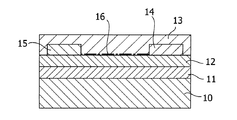
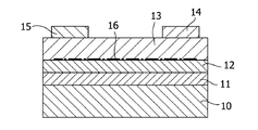
即ち、有機薄膜トランジスタの代表的な構造は図3に示すようなボトムコンタクトと呼ばれるもの、図4に示すようなトップコンタクトと呼ばれるもの、及び図10に示すトップゲートと呼ばれるものに大別される。
ボトムコンタクトにおいてはゲート絶縁膜上にソース電極とドレイン電極が直接、あるいは接着層を介して形成され、その後、有機電子材料膜が形成されてなる。一方、トップコンタクトにおいてはゲート絶縁膜上に有機電子材料膜が形成された後、その上にソース電極とドレイン電極が形成される。これら2つはゲートが基板側に形成される(ボトムゲート)。
一方、トップゲート構造においてはゲートが膜表面側に形成される。このトップゲート構造は特に有機電子材料膜がアモルファスで表面が平滑なポリマー系材料の場合に多く用いられている。
いずれの場合もゲート電極に印加されるゲート電圧により、有機電子材料膜のゲート絶縁膜に接した部分に電荷が誘起され、その電荷がソース電極とドレイン電極との間に印加された電圧により移動することにより電流が流れる。このソース電極とドレイン電極の間の電流経路はチャネルと呼ばれるものである。チャネルは、通常ゲート絶縁膜に接した有機電子材料膜の数分子層の極薄い部分に形成される。
That is, the typical structure of the organic thin film transistor is roughly divided into a structure called a bottom contact as shown in FIG. 3, a structure called a top contact as shown in FIG. 4, and a structure called a top gate as shown in FIG.
In the bottom contact, a source electrode and a drain electrode are formed directly or via an adhesive layer on the gate insulating film, and then an organic electronic material film is formed. On the other hand, in the top contact, after an organic electronic material film is formed on the gate insulating film, a source electrode and a drain electrode are formed thereon. In these two, the gate is formed on the substrate side (bottom gate).
On the other hand, in the top gate structure, the gate is formed on the film surface side. This top gate structure is often used especially when the organic electronic material film is amorphous and the surface of the polymer material is smooth.
In either case, the gate voltage applied to the gate electrode induces a charge in the portion of the organic electronic material film in contact with the gate insulating film, and the charge is moved by the voltage applied between the source electrode and the drain electrode. Current flows. This current path between the source electrode and the drain electrode is called a channel. The channel is usually formed in an extremely thin portion of several molecular layers of the organic electronic material film in contact with the gate insulating film.
有機薄膜トランジスタに用いられる有機電子材料としてはペンタセン、チオフェン系ポリマー、フルオレンチオフェン系ポリマー、銅フタロシアニン、フラーレンなどがあげられる。このうち特に低分子系のペンタセン、銅フタロシアニン、フラーレンなどの材料は、室温では溶剤に溶解せず、一般には真空蒸着で形成される。一方、チオフェン系ポリマー、フルオレン/チオフェン系ポリマーは溶剤に可溶であり、塗布により薄膜形成が可能であるので、真空プロセスを用いる必要がなく、更なる低コスト化が可能である。 Examples of the organic electronic material used for the organic thin film transistor include pentacene, thiophene-based polymer, fluorenethiophene-based polymer, copper phthalocyanine, and fullerene. Among these, materials such as low molecular weight pentacene, copper phthalocyanine, and fullerene are not dissolved in a solvent at room temperature and are generally formed by vacuum deposition. On the other hand, the thiophene polymer and the fluorene / thiophene polymer are soluble in a solvent and can be formed into a thin film by coating. Therefore, it is not necessary to use a vacuum process, and the cost can be further reduced.
しかしながら、これらの有機電子材料薄膜の電荷移動度は最も高いペンタセンでも8cm2/Vs以下に止まっており、現在有機ELディスプレイの駆動に用いられているポリシリコンの10〜100cm2/Vsに比して小さい。特に塗布形成が可能なポリマー系材料の移動度は更に小さく0.1cm2/Vs以下の値が報告されている。 However, the charge mobility of these organic electronic material thin films remains at 8 cm 2 / Vs or less even with the highest pentacene, compared with 10 to 100 cm 2 / Vs of polysilicon currently used for driving organic EL displays. Small. In particular, the mobility of polymer materials that can be coated and formed is even smaller, and a value of 0.1 cm 2 / Vs or less has been reported.
例えば一般に電界効果型トランジスタの飽和電流Isdは、下式で表される。
Isd=(W/2L)*C*μ*(Vg−Vth)2 (1)
For example, the saturation current Isd of a field effect transistor is generally expressed by the following equation.
Isd = (W / 2L) * C * μ * (Vg−Vth) 2 (1)
ここで、WとLはトランジスタのチャネル幅とチャネル長、Cはゲート絶縁膜の単位面積当りの静電容量、μは電子材料の電荷移動度、Vgはゲート電圧、Vthはゲート電圧の閾値電圧である。一定の電圧条件で充分大きなIsdを得るには、C、μが大きいことが望まれるが、これらは用いる材料により定まる物性値である。またWは素子を形成する面積に制限される。Lは例えばフォトリソグラフにより原理的には数10nmまで小さくすることは可能である。即ち、Lを小さくすることにより電荷移動度が小さな材料でも大きなIsdを得ることが可能となる。 Here, W and L are the channel width and channel length of the transistor, C is the capacitance per unit area of the gate insulating film, μ is the charge mobility of the electronic material, Vg is the gate voltage, and Vth is the threshold voltage of the gate voltage. It is. In order to obtain a sufficiently large Isd under a constant voltage condition, it is desirable that C and μ are large, but these are physical property values determined by the material used. W is limited to the area for forming the element. L can be reduced to several tens of nanometers in principle by, for example, photolithography. That is, by reducing L, a large Isd can be obtained even with a material having a small charge mobility.
しかしながら、小さなLを得るためには一般には高価なプロセスが必要となる。例えば、通常のフォトプロセスは加工精度は高いが一般に高コストであり、特に数μm以下の加工精度を得るには高価な設備が必要とされる。
また、特に塗布形成可能な導電性材料では、従来各種の印刷(例えばIJP、パッド印刷、フレキソ印刷、グラビア印刷)により電極形成がなされる場合もあった。しかしながら、これらの方法での寸法精度はおおよそ20μmが限界であり、上記目的に必要な10μm以下のチャネル長を精度良く得るのは困難であった。
However, in order to obtain small L, generally an expensive process is required. For example, a normal photo process has high processing accuracy but is generally high in cost, and particularly expensive equipment is required to obtain processing accuracy of several μm or less.
In particular, for conductive materials that can be formed by coating, electrodes may be formed by various types of printing (for example, IJP, pad printing, flexographic printing, and gravure printing). However, the dimensional accuracy in these methods is limited to approximately 20 μm, and it has been difficult to accurately obtain a channel length of 10 μm or less necessary for the above purpose.
これに加えて、特に基板として安価なプラスチック基板を用いる場合は基板の熱膨張率が大きくなるので、別個のパターニングプロセス間でのパターン位置の整合性を取ることが困難になる。上記のチャネル幅Wとチャネル長Lは、その精度が直接トランジスタ特性に反映されるので、少なくともソース電極とドレイン電極とは、一回のパターニングプロセスで再現性が高い方法で精度良く形成されることが望まれていた。
このように、有機材料の特長を生かすために、有機薄膜トランジスタを、安価、かつ高い寸法精度で形成する方法が強く望まれていた。
Thus, in order to take advantage of the characteristics of the organic material, a method for forming an organic thin film transistor with low cost and high dimensional accuracy has been strongly desired.
よって本発明の目的は、上述の点に鑑み、有機薄膜トランジスタにおいて、ソース電極、ドレイン電極の高精度の微細加工をプラスチック基板などの上に安価なプロセスで実現し、高い性能を安定して実現する手段を提供することである。 Therefore, in view of the above points, an object of the present invention is to realize high-precision microfabrication of a source electrode and a drain electrode on an organic thin film transistor by a low-cost process on a plastic substrate and stably achieve high performance. Is to provide a means.
本発明は、上記課題を解決するためになされたものである。すなわち、本発明に係る薄膜トランジスタは、上記目的を達成するために、基板と、ソース電極およびドレイン電極上に形成された有機電子材料膜と、有機電子材料膜上に形成されたゲート絶縁膜と、ゲート絶縁膜上に形成されたゲート電極とを含む薄膜トランジスタであって、前記ソース電極およびドレイン電極が、前記基板に形成された溝または穴に埋め込まれ、前記有機電子材料膜と電気的に接触していることを特徴とする。
本発明に係る薄膜トランジスタの製造方法は、基板に溝または穴を形成するステップと、前記溝または穴にソース電極およびドレイン電極を形成するステップと、前記ソース電極およびドレイン電極を形成した基板上に有機電子材料膜、ゲート絶縁膜、および、ゲート電極をこの順で形成するステップとを含むことを特徴とする。
The present invention has been made to solve the above problems. That is, in order to achieve the above object, the thin film transistor according to the present invention includes a substrate, an organic electronic material film formed on the source electrode and the drain electrode, a gate insulating film formed on the organic electronic material film, A thin film transistor including a gate electrode formed on a gate insulating film, wherein the source electrode and the drain electrode are embedded in a groove or a hole formed in the substrate and are in electrical contact with the organic electronic material film. It is characterized by.
A method of manufacturing a thin film transistor according to the present invention includes: forming a groove or a hole in a substrate; forming a source electrode and a drain electrode in the groove or hole; Forming an electronic material film, a gate insulating film, and a gate electrode in this order.
本発明によれば、有機薄膜トランジスタにおいて、ソース電極、ドレイン電極の高精度の微細加工をプラスチック基板などの上に安価なプロセスで実現し、高い性能を安定して実現する手段を提供することが出来る。加えて、ソース電極、ドレイン電極へのマトリックス状の配線を簡便にし、かつ、素子からのリーク電流を低減する手段を提供することが出来る。 According to the present invention, in an organic thin film transistor, it is possible to provide a means for stably realizing high performance by realizing high-precision fine processing of a source electrode and a drain electrode on a plastic substrate or the like by an inexpensive process. . In addition, it is possible to provide means for simplifying the matrix wiring to the source electrode and the drain electrode and reducing the leakage current from the element.
本発明においては、有機電子材料膜、ゲート絶縁膜、ゲート電極が積層して形成され、別個に形成されたソース電極とドレイン電極との間の電流が上記ゲート絶縁膜に接した有機電子材料膜を介して流れ、かつ、上記電流が上記ゲート電極の電位により制御される薄膜電界効果トランジスタであって、上記ソース電極とドレイン電極とが、基板に形成された溝または穴に埋め込まれ、上記有機電子材料膜、ゲート絶縁膜、ゲート電極が、その上に形成されてなることとした。 In the present invention, an organic electronic material film, a gate insulating film, and a gate electrode are stacked, and an organic electronic material film in which a current between a source electrode and a drain electrode formed separately is in contact with the gate insulating film. And the current is controlled by the potential of the gate electrode, wherein the source electrode and the drain electrode are embedded in a groove or hole formed in a substrate, and the organic An electronic material film, a gate insulating film, and a gate electrode are formed thereon.
上記基板の溝または穴の形成は、熱インプリントによることが好ましい。
基材の材質として熱可塑性のプラスチック材料を用いる場合、例えば、押し出し成型などの方法でも所望の溝を形成した基板を作製することは可能である。しかしながら、押し出し成型では基板寸法が金型寸法により制限される。これに対し、熱インプリントは、ガラス転移点以上に加熱された基板に、溝または穴の形成に必要な鋳型を押し付ける方法である。従って、基本的に基板寸法に制限はなく、大面積基板に連続的に溝形成をするのに適した方法である。
基板の材質として、光硬化樹脂を用いることもできるが、その場合、鋳型による成型の後、光照射により硬化させることにより溝または穴を形成する。この場合は、硬化後の樹脂が弾性に乏しくなるので、例えば、製品として可撓性が求められる場合には作製条件に細かな注意が必要となる。
The formation of the groove or hole in the substrate is preferably performed by thermal imprint.
When a thermoplastic plastic material is used as the material of the base material, it is possible to produce a substrate having a desired groove formed by, for example, an extrusion molding method. However, in extrusion molding, the substrate dimensions are limited by the mold dimensions. On the other hand, thermal imprinting is a method in which a mold necessary for forming a groove or a hole is pressed against a substrate heated above the glass transition point. Therefore, there is basically no limitation on the substrate size, and this method is suitable for continuously forming grooves in a large-area substrate.
A photo-curing resin can be used as the material of the substrate. In that case, after molding with a mold, a groove or a hole is formed by curing by light irradiation. In this case, since the resin after curing becomes poor in elasticity, for example, when flexibility is required as a product, careful attention is required for the production conditions.
上記溝または穴の形成の際の基板の加熱温度としては、用いる基板の材質にもよるが、通常、100℃〜300℃である。
上記溝または穴の形成のために基板にかける圧力としては、通常、10〜200MPaである。
上記溝または穴の形成に用いる鋳型の材質としては特に限定されず、例えば、
シリコン、シリコンカーバイド、サファイア、ダイヤモンド、タンタル、SiO2/Si、SiN/Si等が挙げられる。鋳型は、予め、加熱しておくことが好ましく、加熱温度としては、100〜350℃であることが好ましい。
上記溝または穴ひとつの幅は、鋳型の厚みにもよるが、通常、10nm〜50μmである。
本発明の薄膜トランジスタの製造方法によれば、基板面積が100nm2以上、より好ましくは、1μm2以上の薄膜トランジスタを得ることができる。
The substrate heating temperature in forming the groove or hole is usually 100 ° C. to 300 ° C., although it depends on the material of the substrate used.
The pressure applied to the substrate for forming the groove or hole is usually 10 to 200 MPa.
The material of the mold used for forming the groove or hole is not particularly limited, for example,
Examples thereof include silicon, silicon carbide, sapphire, diamond, tantalum, SiO 2 / Si, and SiN / Si. The mold is preferably heated in advance, and the heating temperature is preferably 100 to 350 ° C.
The width of each groove or hole is usually 10 nm to 50 μm, although it depends on the thickness of the mold.
According to the method for producing a thin film transistor of the present invention, a thin film transistor having a substrate area of 100 nm 2 or more, more preferably 1 μm 2 or more can be obtained.
上記溝または穴同士の間隔が、チャネル長に相当する。本発明によれば、チャネル長は、1〜50μmとすることができる。チャネル長の好ましい上限は、30μm、より好ましい上限は、12μmである。 The interval between the grooves or holes corresponds to the channel length. According to the present invention, the channel length can be 1 to 50 μm. A preferable upper limit of the channel length is 30 μm, and a more preferable upper limit is 12 μm.
また、上記ソース電極またはドレイン電極の形成は、導電性材料溶液もしくは導電性材料分散液を、基板に形成された溝または穴に注入することが好ましい。この方法によれば、溝または穴のアスペクト比が高い場合でも溶液または分散液が表面張力による毛細管現象で溝または穴へ注入されるので、その他の膜形成手段(例えば真空蒸着など)に比して容易に電極形成が可能である。また、ソース電極、ドレイン電極は、高価なフォトリソグラフなどの手段を用いることなく、安価に高精度で再現性良く形成することが可能となる。 The source electrode or the drain electrode is preferably formed by injecting a conductive material solution or a conductive material dispersion into a groove or a hole formed in the substrate. According to this method, even when the aspect ratio of the groove or hole is high, the solution or dispersion liquid is injected into the groove or hole by capillary action due to surface tension. Therefore, compared with other film forming means (for example, vacuum deposition). Thus, the electrode can be easily formed. Further, the source electrode and the drain electrode can be formed inexpensively with high accuracy and good reproducibility without using expensive means such as photolithography.
また、ソース電極、もしくはドレイン電極の少なくとも一方が基板を貫通し、上記有機電子材料膜、ゲート絶縁膜、ゲート電極が存在する基板面に対して反対の基板面において電気的に接続されてなることが好ましい。このような構成とすることにより、ソース電極の配線とドレイン電極の配線とが基板の互いに反対面でなされるので、例えば、ディスプレイ駆動で必要とされるマトリックス状の配線が簡便になるという利点が生じる。即ち、薄膜トランジスタのソース電極側の引き出し線とドレイン電極側の引き出し線とが直交する構成でも、各配線は基板の互いに反対面に形成されるので、その交点に絶縁膜を形成する必要がない。また、特に好ましい態様としては、一方の電極が基板を貫通していることで、他方の電極に完全に包囲される構造が挙げられる。
基板を貫通した電極は、電気的接続を確実にするため、上記有機電子材料膜、ゲート絶縁膜、ゲート電極が存在する基板面に対して反対の基板面において、補助的な電極を設けてもよい。
Further, at least one of the source electrode and the drain electrode penetrates the substrate and is electrically connected to the substrate surface opposite to the substrate surface on which the organic electronic material film, the gate insulating film, and the gate electrode are present. Is preferred. By adopting such a configuration, the wiring of the source electrode and the wiring of the drain electrode are made on opposite surfaces of the substrate, so that, for example, there is an advantage that the matrix-like wiring required for display driving becomes simple. Arise. That is, even in a configuration in which the lead line on the source electrode side and the lead line on the drain electrode side of the thin film transistor are orthogonal to each other, each wiring is formed on the opposite surface of the substrate. Moreover, as a particularly preferable aspect, there is a structure in which one electrode penetrates the substrate and is completely surrounded by the other electrode.
In order to ensure electrical connection, the electrode penetrating the substrate may be provided with an auxiliary electrode on the substrate surface opposite to the substrate surface on which the organic electronic material film, the gate insulating film, and the gate electrode exist. Good.
また、上記ソース電極、もしくはドレイン電極のうち、一方の電極が、基板面内で他方の電極の外縁に沿って形成されたものであることが好ましい。
本明細書において、「外縁に沿って形成」とは、一方の電極の輪郭の少なくとも一部分が、距離を隔てて他方の電極の輪郭の一部分を覆うように形成されていることをいう。
従って、一方の電極が、基板面内で他方の電極の外縁に沿って形成されたという場合、一方の電極が、他方の電極によって包囲されているものに限定されず、電極同士が、互いに噛み合ったくし形構造になるように形成されているものであってもよい。
In addition, it is preferable that one of the source electrode and the drain electrode is formed along the outer edge of the other electrode within the substrate surface.
In this specification, “formed along the outer edge” means that at least a part of the outline of one electrode is formed to cover a part of the outline of the other electrode at a distance.
Therefore, when one electrode is formed along the outer edge of the other electrode within the substrate surface, the one electrode is not limited to be surrounded by the other electrode, and the electrodes mesh with each other. It may be formed so as to have a comb-shaped structure.
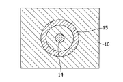
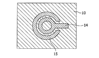
本発明の薄膜トランジスタは、ソース電極またはドレイン電極の一方が、基板面内で他方の電極に包囲されたものであることがより好ましい。
例えば、ドレイン電極を円柱状とし、ソース電極をその周囲にドーナツ状に形成することにより、ソース電極が所謂ガードリングの機能を持ち、リーク電流を抑制することが可能である。特に上記ドーナツ状の形状を、内部電極に対して閉じたものとすることはフォトリソグラフでは2回以上の露光が必要であり位置合わせなど難度が高い作業となるが、本発明の熱インプリントによれば一回の作業ですみ、かつ、両電極の相対位置がずれるおそれがない点において好ましい。
In the thin film transistor of the present invention, it is more preferable that one of the source electrode and the drain electrode is surrounded by the other electrode within the substrate surface.
For example, by forming the drain electrode in a cylindrical shape and forming the source electrode in a donut shape around the drain electrode, the source electrode has a so-called guard ring function, and leakage current can be suppressed. In particular, making the doughnut-shaped shape closed with respect to the internal electrode requires exposure twice or more in photolithography, which is a difficult task such as alignment. Therefore, it is preferable in that it requires only one operation and there is no possibility that the relative positions of both electrodes are shifted.
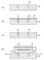
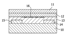
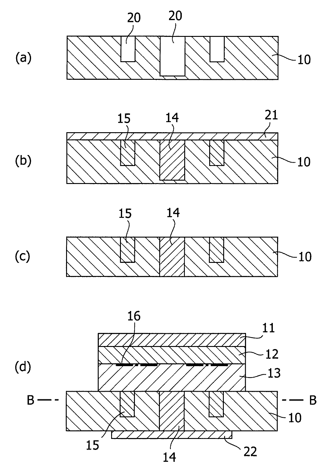
本発明の薄膜トランジスタの作製プロセスと構造の第1の例を図1に示す。熱可塑性プラスチック基板10上に加熱された鋳型を押し付けて、溝20を形成する(図1(a))。その後、当該基板に導電性材料溶液もしくは導電性材料分散液を塗布する。それらの溶液もしくは分散液は、表面張力により上記溝内に注入される(図1(b))。この注入を容易にするには、予め、溝内をオゾン暴露処理や各種親水処理材での被覆などにより親水化しておくことも可能である。塗布した溶液もしくは分散液を乾燥、固化させた後、酸素プラズマなどにより、溝外の導電性材料21を除去することにより、基板内にソース電極とドレイン電極とが一定の距離を隔てた構造が形成される(図1(c))。
なお、塗布した溶液もしくは分散液を乾燥させると体積収縮により溝または穴内に空隙が生じる場合があるが、電気的接続が取れれば機能的問題は生じない。別の理由で空隙を埋める必要がある場合は比較的高い濃度の溶液を用い、重ね塗りをするなどの方法を用いることも可能である。
このソース電極およびドレイン電極を形成した基板上に有機電子材料膜、ゲート絶縁膜、ゲート電極が順次、真空蒸着、スピンコート、印刷等の方法で形成される(図1(d))。電荷のチャネル16は、ソース電極とドレイン電極との間の、有機電子材料膜内における、ゲート絶縁膜との界面近傍に形成される。図5にはこの構造の、図1(d) A−A断面での平面図を示した。
A first example of a manufacturing process and structure of a thin film transistor of the present invention is shown in FIG. A heated mold is pressed onto the
When the applied solution or dispersion is dried, voids may be generated in the grooves or holes due to volume shrinkage. However, if electrical connection is established, no functional problem will occur. When it is necessary to fill the gap for another reason, it is possible to use a method of using a relatively high concentration solution and overcoating.
An organic electronic material film, a gate insulating film, and a gate electrode are sequentially formed on the substrate on which the source and drain electrodes are formed by a method such as vacuum deposition, spin coating, and printing (FIG. 1D). The
図6には、本発明の薄膜トランジスタの作製プロセスと構造の第2の例を示す。これにおいては、ドレイン電極14はソース電極15より深く形成され(図6(a)、(b))、導電性材料の注入後、溝外の導電性材料21の除去と前後して、基板の反対面をエッチングすることにより、ドレイン電極14は反対面まで貫通させられる(図6(c))。その後、有機電子材料膜13、ゲート絶縁膜12、ゲート電極11が、上記の第1の例と同様にして形成されるが、ドレイン電極14については、反対面での電気的接続を確実にするための電極22を形成することも必要に応じて可能である(図6(d))。
図7にはこの構造の、図6(d) B−B断面での平面図を示した。この例では、ソース電極はドレイン電極の外縁に沿って形成されガードリングの機能を果たすので、ドレイン電圧によるリーク電流が発生しにくい構成となっている。このように閉じた曲線を多重とする構成はフォトリソグラフなどのマスクを使用する方法では(内部の形状を決めるマスクを支える構造が無いので)一回のプロセスでは形成することができないが、本発明の方法では、鋳型が作製してあれば、容易に形成することが可能である。
FIG. 6 shows a second example of a manufacturing process and structure of a thin film transistor of the present invention. In this case, the
FIG. 7 shows a plan view of this structure on the BB cross section of FIG. In this example, since the source electrode is formed along the outer edge of the drain electrode and functions as a guard ring, a leak current due to the drain voltage is hardly generated. Such a configuration in which closed curves are multiplexed cannot be formed in a single process by a method using a mask such as a photolithograph (since there is no structure that supports a mask for determining the internal shape), but the present invention In this method, if a template is prepared, it can be easily formed.
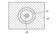
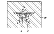
第3の例として、図8に示すように内側の電極を外側の電極と同様にドーナツ形とすることも容易である。この場合は図7に比して溝面積が小さくなり、表面張力による導電性材料液の注入が容易となるが、電極を貫通させる場合は、その内側の基板が導電性材料を介して支えられる構造となる。また、第4の例として、図9に示すように、電極の平面形状を異形として外縁長さを大きくすることにより、チャネル幅を大きくしてトランジスタの飽和電流Isdを大きくすることももちろん可能である。 As a third example, as shown in FIG. 8, it is easy to make the inner electrode into a donut shape like the outer electrode. In this case, the groove area is smaller than that in FIG. 7 and the injection of the conductive material liquid by the surface tension is facilitated. However, when the electrode is penetrated, the inner substrate is supported by the conductive material. It becomes a structure. Further, as a fourth example, as shown in FIG. 9, it is of course possible to increase the saturation current Isd of the transistor by increasing the outer edge length by making the planar shape of the electrode irregular and increasing the channel width. is there.
また、上記の例では電極が貫通しない場合に図5の平面形状、電極が貫通する場合に図7、図8、および図9の平面形状を組み合わせて説明したが、ソース電極とドレイン電極とが逆の組み合わせも当然可能である。 Further, in the above example, the planar shape of FIG. 5 is described when the electrode does not penetrate, and the planar shapes of FIGS. 7, 8, and 9 are combined when the electrode penetrates. The reverse combination is naturally possible.
このように形成された本発明の薄膜トランジスタを、従来の素子構造、即ち図3のボトムコンタクト、図4のトップコンタクト、図10のトップゲートと比較すると、ボトムコンタクトとトップゲート構造ではソース電極、ドレイン電極はフォトリソグラフ等の方法で形成されるので、高価な設備と多くのプロセスが必要であったのに対し、本発明の製造方法によれば、設備投資が少なくプロセスも簡便であるという特長を有する。このコスト差はチャネル長が10μm以下の加工を行う場合に特に顕著となるものである。
またトップコンタクトにおけるソース電極およびドレイン電極の形成は元来シャドウマスクにより行われるので、チャネル長30μm以下の形成は困難であった。
このようにして、本発明においては、従来の素子構造の問題点を回避し、高精度の微細加工を安価なプロセスで実現する手段を提供することが出来る。
Compared with the conventional device structure, that is, the bottom contact in FIG. 3, the top contact in FIG. 4, and the top gate in FIG. 10, the thin film transistor of the present invention formed in this way has a source electrode and drain in the bottom contact and top gate structure. Since the electrode is formed by a method such as photolithography, expensive equipment and many processes are required. On the other hand, the manufacturing method of the present invention has the feature that the equipment investment is small and the process is simple. Have. This cost difference is particularly noticeable when processing with a channel length of 10 μm or less.
In addition, since the source electrode and the drain electrode in the top contact are originally formed using a shadow mask, it is difficult to form a channel length of 30 μm or less.
Thus, in the present invention, it is possible to avoid the problems of the conventional element structure and to provide means for realizing high-precision fine processing by an inexpensive process.
本発明においては、有機電子材料としては、例えば、ペンタセン、テトラセン、アントラセンなどのアセン系化合物の他、ルブレン、チオフェン、ヘキシルチオフェン系ポリマー、フルオレン/チオフェン系ポリマー、銅フタロシアニン、フラーレン等の材料が好適であるがそれに限定されるものではなく、多くの有機電子材料が適用可能である。 In the present invention, as the organic electronic material, for example, a material such as rubrene, thiophene, hexylthiophene polymer, fluorene / thiophene polymer, copper phthalocyanine, fullerene, in addition to acene compounds such as pentacene, tetracene, and anthracene are suitable. However, the present invention is not limited to this, and many organic electronic materials can be applied.
ソース電極およびドレイン電極については各種金属材料、有機導電性材料が適用可能であるが、例えば、有機電子材料を移動する電荷がホールである場合は、ソース電極でのホールの注入を促進し、かつドレイン電極での電子の注入を抑制するため、電極材料としては仕事関数の大きい材料が好適である。特に金属材料としては、分散液として形成しやすい、Au、Ag、Ptなどの微細粒子を主成分とするものが好適である。また、有機導電性材料としては、例えば、ポリ−3,4−エチレンジオキシチオフェン/ポリスチレンスルホネート(PEDOT/PSS)やポリアニリン(PANI)が好適である。 Various metal materials and organic conductive materials can be applied to the source electrode and the drain electrode. For example, when the charge moving through the organic electronic material is a hole, the injection of the hole at the source electrode is promoted, and In order to suppress injection of electrons at the drain electrode, a material having a high work function is preferable as the electrode material. Particularly preferred as the metal material is a material mainly composed of fine particles such as Au, Ag, and Pt, which can be easily formed as a dispersion. As the organic conductive material, for example, poly-3,4-ethylenedioxythiophene / polystyrene sulfonate (PEDOT / PSS) and polyaniline (PANI) are suitable.
ゲート絶縁膜としては、各種金属酸化物、例えば、シリコン、アルミニウム、タンタル、チタン、ストロンチウム、バリウムなどの酸化物、これら酸化物の混合酸化物を用いることが可能である。また、高分子材料、例えばポリスチレン、ポリビニールアルコール、ポリビニールフェノール、アクリルなどのポリマー材料も用いることが出来る。また、これらの高分子材料に金属酸化物を分散して用いることも可能である。特に金属酸化物は高分子材料に比して誘電率が高い材料が多く、トランジスタを比較的低電圧で駆動することが可能であるという特徴を有する。これに対し高分子材料は比較的誘電率が低いので、高速応答性がよいという特徴がある。 As the gate insulating film, various metal oxides, for example, oxides such as silicon, aluminum, tantalum, titanium, strontium, and barium, and mixed oxides of these oxides can be used. Further, polymer materials such as polymer materials such as polystyrene, polyvinyl alcohol, polyvinyl phenol, and acrylic can also be used. Further, it is also possible to use a metal oxide dispersed in these polymer materials. In particular, many metal oxides have a dielectric constant higher than that of a polymer material, and the transistor can be driven at a relatively low voltage. On the other hand, the polymer material has a characteristic that the high-speed response is good because the dielectric constant is relatively low.
ゲート電極については、各種金属材料、有機導電性材料が適用可能であるが、ゲート絶縁膜への密着性や形成の容易さなどを勘案して決定される。 Various metal materials and organic conductive materials can be applied to the gate electrode, but the gate electrode is determined in consideration of adhesion to the gate insulating film and ease of formation.
また、これらの素子を形成する基板の材質としては、各種の基板が可能であるが、熱インプリントにより溝または穴の形成を行う場合は熱可塑性のプラスチック材料を用いることが好ましい。
熱可塑性のプラスチック材料としては特に限定されず、例えば、ポリエーテルイミド(PEI)、 ポリエーテルエーテルケトン(PEEK)、ポリエチレンテレフタレート(PET)、ポリエチレンナフタレート(PEN)、ポリエーテルサルフォン(PES)、ポリフェニレンサルファイド(PPS)、ポリカーボネート(PC)、ポリスチレン(PS)、ポリメチルメタクリレート(PMMA)などの高分子フィルムを用いることが出来る。
In addition, various substrates can be used as a material for the substrate on which these elements are formed. However, when grooves or holes are formed by thermal imprinting, it is preferable to use a thermoplastic plastic material.
The thermoplastic plastic material is not particularly limited. For example, polyetherimide (PEI), polyetheretherketone (PEEK), polyethylene terephthalate (PET), polyethylene naphthalate (PEN), polyethersulfone (PES), Polymer films such as polyphenylene sulfide (PPS), polycarbonate (PC), polystyrene (PS), and polymethyl methacrylate (PMMA) can be used.
本発明の薄膜トランジスタにおけるアスペクト比は、好ましくは、1〜40である。上記アスペクト比のより好ましい上限は、30、より好ましい下限は、3である。 The aspect ratio of the thin film transistor of the present invention is preferably 1 to 40. A more preferable upper limit of the aspect ratio is 30, and a more preferable lower limit is 3.
以下に、本発明を、図面を参照して詳細に説明する。同じ部材には同じ符号を付して表した。なお、本発明は以下に説明する形態に制限されるものではない。 Hereinafter, the present invention will be described in detail with reference to the drawings. The same members are denoted by the same reference numerals. In addition, this invention is not restrict | limited to the form demonstrated below.
ポリエチレンナフタレート(PEN)基板(厚さ100μm)10を220℃に加熱し、これに別途形成したシリコン製の鋳型を270℃に加熱して押し込むことにより、20 x 100μm(100μmがチャネル幅に相当)、深さ60μmの溝を2本、間隔10μm(チャネル長に相当)で形成した。この溝部に波長254nmの紫外光を照射して親水化した後、導電性材料液としてPEDOT:PSS溶液(Bayer社製、Al4083)をスピンコート法により塗布した。スピンコートの回転数は1000rpm、回転時間は180秒であった。塗布したPEDOT:PSS溶液が溝内へ毛細管現象で浸入するのを確認後、これに120℃、10分の乾燥処理を施した。
次に、酸素プラズマにより溝外のPEDOT:PSSをエッチングして、2本の溝の電気的絶縁を確保した。この時、外部回路との電気的接続を得るための導電部はマスクによりエッチングを避けて確保した。
A polyethylene naphthalate (PEN) substrate (thickness 100 μm) 10 is heated to 220 ° C., and a silicon mold separately formed is heated to 270 ° C. and pressed into it, so that 20 × 100 μm (100 μm corresponds to the channel width) ), Two grooves having a depth of 60 μm were formed at an interval of 10 μm (corresponding to a channel length). The groove was irradiated with ultraviolet light having a wavelength of 254 nm to make it hydrophilic, and then a PEDOT: PSS solution (manufactured by Bayer, Al4083) was applied as a conductive material solution by a spin coating method. The rotation speed of the spin coat was 1000 rpm, and the rotation time was 180 seconds. After confirming that the applied PEDOT: PSS solution entered into the groove by capillary action, this was subjected to a drying treatment at 120 ° C. for 10 minutes.
Next, PEDOT: PSS outside the groove was etched with oxygen plasma to ensure electrical insulation of the two grooves. At this time, a conductive portion for obtaining electrical connection with an external circuit was secured by avoiding etching with a mask.
次にチオフェン系ポリマー、ポリ(3−ヘキシルチオフェン)(P3HT)(メルク社製)をp−キシレン中に2mg/mLの濃度で溶解させ、これをスピンコートすることにより厚さ30nmの有機電子材料膜13を得た。その後、ポリスチレン(アルドリッチ社製)を酢酸エチル中に70mg/mlの濃度で溶解させ、これをスピンコートすることにより厚さ300nmのゲート絶縁膜を得た。最後にアルミニウムをポリスチレンゲート絶縁膜上に真空蒸着することにより、膜厚60nmのゲート電極を得た。このようにして実施例1の試料を得た。
Next, a thiophene polymer, poly (3-hexylthiophene) (P3HT) (manufactured by Merck & Co., Inc.) is dissolved in p-xylene at a concentration of 2 mg / mL, and spin coated to form an organic electronic material having a thickness of 30 nm. A
厚さ100μmのポリエチレンナフタレート(PEN) シートに20x100μm(100μmがチャネル幅に相当)、深さ60μmの溝を2本、間隔5μm(チャネル長に相当)で形成した基板を押し出し成形で作製し、これを基板として用いた他は実施例1と同様にして実施例2の試料を得た。 A substrate formed of a polyethylene naphthalate (PEN) sheet having a thickness of 100 μm with 20 × 100 μm (100 μm corresponding to the channel width), two grooves with a depth of 60 μm, and an interval of 5 μm (corresponding to the channel length) is produced by extrusion molding. A sample of Example 2 was obtained in the same manner as Example 1 except that this was used as a substrate.
導電性材料液としてAg微粒子分散液(ナノメタルインク、真空冶金株式会社製)を用い、乾燥条件を150℃、120分とした。また、溝部以外の導電部のエッチングを希硝酸によって行った以外は実施例1と同様にして実施例3の試料を得た。 An Ag fine particle dispersion (Nano Metal Ink, manufactured by Vacuum Metallurgical Co., Ltd.) was used as the conductive material liquid, and the drying conditions were 150 ° C. and 120 minutes. A sample of Example 3 was obtained in the same manner as in Example 1 except that etching of the conductive part other than the groove part was performed with diluted nitric acid.
ポリエチレンテレフタレート(PET)基板(厚さ50μm)10を200℃に加熱し、これに別途形成したシリコン製の鋳型を260℃に加熱して押し込むことにより、内径30μmx外径40μm、深さ30μmの溝と、内径50μmx外径60μm、深さ45μmの溝とを同心円状に形成した。両溝の間隔10μmがチャネル長、チャネルに面する溝円周(各40、50μm)がチャネル幅に相当する。実施例1と同様にして、波長254nmの紫外光を照射して親水化した後、導電性材料液としてPEDOT:PSS溶液(Bayer社製、Al4083)をスピンコート法により塗布した。その後、基板の反対面を酸素プラズマエッチにより研磨して外周溝にドレイン電極を貫通させた。次に実施例1と同様にして有機電子材料膜13としてチオフェン系ポリマー、ポリ(3−ヘキシルチオフェン)(P3HT)(メルク社製)をp−キシレン中に2mg/mLの濃度で溶解させ、これをスピンコートすることにより厚さ30nmの膜を得た。その後、ポリスチレン(アルドリッチ社製)を酢酸エチル中に70mg/mlの濃度で溶解させ、これをスピンコートすることにより厚さ300nmの膜を得た。最後にアルミニウムをポリスチレンゲート絶縁膜上に真空蒸着することにより、膜厚60nmで成膜してゲート電極とした。このようにして実施例4の試料を得た。
A polyethylene terephthalate (PET) substrate (thickness 50 μm) 10 is heated to 200 ° C., and a silicon mold separately formed therein is heated to 260 ° C. and pressed into a groove having an inner diameter of 30 μm × an outer diameter of 40 μm and a depth of 30 μm. A groove having an inner diameter of 50 μm, an outer diameter of 60 μm, and a depth of 45 μm was formed concentrically. The interval between both grooves corresponds to the channel length, and the groove circumference (each 40, 50 μm) facing the channel corresponds to the channel width. In the same manner as in Example 1, after making hydrophilic by irradiating with ultraviolet light having a wavelength of 254 nm, a PEDOT: PSS solution (manufactured by Bayer, Al4083) was applied as a conductive material solution by a spin coat method. Thereafter, the opposite surface of the substrate was polished by oxygen plasma etching, and the drain electrode was passed through the outer peripheral groove. Next, in the same manner as in Example 1, a thiophene polymer, poly (3-hexylthiophene) (P3HT) (manufactured by Merck) was dissolved as an organic
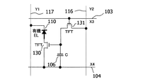
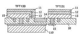
実施例4と同様の方法で、薄膜トランジスタを2個1組で100組、10行x10列のマトリックス状に形成した。また1組のトランジスタにキャパシタと発光素子を付加して図2に示す回路を構成した。2個の薄膜トランジスタは図12に示すように、基板に対してゲート電極を同じ側に形成し、スイッチング用TFTでは貫通電極をソース電極、外側電極をドレイン電極として用いた。即ち、行電極線1:103、行電極線2:104、キャパシタ106は薄膜トランジスタのゲート電極側、発光素子110、列電極線1:116、列電極線2:117はゲート電極の反対側の基板面に配することとした(図12では薄膜トランジスタと発光素子以外は図示を省略)。
In the same manner as in Example 4, two thin film transistors were formed in a matrix of 100 sets, 10 rows × 10 columns. Further, a circuit shown in FIG. 2 is configured by adding a capacitor and a light emitting element to one set of transistors. As shown in FIG. 12, the two thin film transistors were formed with the gate electrode on the same side with respect to the substrate, and the switching TFT used the through electrode as the source electrode and the outer electrode as the drain electrode. That is, the row electrode line 1: 103, the row electrode line 2: 104, the
[比較例1]
実施例1と同様の構造の素子をフォトリソグラフを用いて、従来のトップゲート構造で作製した。即ち、基板上にフォトレジスト(OFPR−800、東京応化工業株式会社)をスピンコートにより厚さ2μmで塗布した後、フォトマスクを通して、紫外光405nm、11mW/cm2を4秒間照射し、照射部を硬化させた。ソース電極とドレイン電極とを形成する部分は、20 x 100μm(100μmがチャネル幅に相当)の像を2本、間隔10μm(チャネル長に相当)とし、この部分はフォトマスクにより紫外光が照射されないようにした。その後、現像液(NMD−3、東京応化工業株式会社),により非照射部を洗い流して現像した後、プリベーク(110℃、90秒)、ポストベーク(130℃、30分)を行った。その上に膜厚100nmの金薄膜を真空蒸着により形成した。更に、フォトレジストをリフトオフにより剥離した後、露出した基板面を波長254nmの紫外光を照射して洗浄し、その上に有機電子材料膜13としてポリ(3−ヘキシルチオフェン)(P3HT)薄膜(メルク社製)、ポリスチレン薄膜、アルミニウム薄膜を実施例1と同様に形成して比較例1の試料を得た。
[Comparative Example 1]
An element having the same structure as that of Example 1 was fabricated with a conventional top gate structure using photolithography. That is, after applying a photoresist (OFPR-800, Tokyo Ohka Kogyo Co., Ltd.) with a thickness of 2 μm on a substrate by spin coating, ultraviolet light of 405 nm and 11 mW / cm 2 are irradiated for 4 seconds through a photomask. Was cured. The portion where the source electrode and the drain electrode are formed has two images of 20 × 100 μm (100 μm corresponds to the channel width) and an interval of 10 μm (corresponds to the channel length), and this portion is not irradiated with ultraviolet light by the photomask I did it. Thereafter, the non-irradiated part was washed away with a developer (NMD-3, Tokyo Ohka Kogyo Co., Ltd.) and developed, and then pre-baked (110 ° C., 90 seconds) and post-baked (130 ° C., 30 minutes). A gold thin film having a thickness of 100 nm was formed thereon by vacuum deposition. Further, after removing the photoresist by lift-off, the exposed substrate surface is cleaned by irradiating with ultraviolet light having a wavelength of 254 nm, and a poly (3-hexylthiophene) (P3HT) thin film (Merck) is formed thereon as the organic
[比較例2]
実施例4と類似の構成を従来の基板面上構造で試作した。即ち、ポリエチレンテレフタレート(PET)基板(厚さ50μm)10上に、内径30μm x 外径40μmのドーナツ状電極と、内径50μm x 外径60μmのドーナツ状電極とを比較例1と同様の方法で形成した。この時、両電極が同一平面上に形成されており、内側電極の電気的接続の必要性から、外側のドーナツ電極の一部は、図11のように切りかけのある形状となる。
[Comparative Example 2]
A structure similar to that of Example 4 was prototyped with a conventional structure on the substrate surface. That is, on a polyethylene terephthalate (PET) substrate (thickness: 50 μm), a donut-shaped electrode having an inner diameter of 30 μm × an outer diameter of 40 μm and a donut-shaped electrode having an inner diameter of 50 μm × an outer diameter of 60 μm are formed in the same manner as in Comparative Example 1. did. At this time, both electrodes are formed on the same plane, and due to the necessity of electrical connection of the inner electrode, a part of the outer donut electrode has a cut shape as shown in FIG.
以上の実施例、比較例の試料の素子特性を表1にまとめた。実施例1、実施例2および実施例3は比較例1に比して移動度や飽和電流Isd(Vg=−20V)の値は同等である(実施例2は、W/Lが実施例1、実施例3、および比較例1の2倍なので、飽和電流Isdは約2倍となっている)。リーク電流も同等であるが、作製した素子100個でのIsdの標準偏差は若干小さくなっており、かつ作業時間(素子100個を作製する時間)は、大幅に短縮されている。これは、比較例1におけるソース/ドレイン電極の形成では、(1)フォトレジスト塗布、(2)紫外光照射、(3)現像、(4)プリベーク、(5)ポストベーク、(6)金薄膜真空蒸着、(7)フォトレジストリフトオフ、(8)基板洗浄、と8ステップのプロセスが必要とされるのに対し、実施例1および実施例2においては、(1)基板への溝形成、(2)導電材料塗布、(3)エッチング、の3ステップであり、かつ各ステップが簡便であるからである。
また、実施例4についても、比較例2に対し作業時間が大幅に短縮されている他、リーク電流は比較例2に対し大きく低減されている。これは比較例2の場合はソース電極によるドレイン電極のガードリング効果が不完全なためと推定される。
Table 1 summarizes the device characteristics of the samples of the above examples and comparative examples. In Example 1, Example 2 and Example 3, the values of mobility and saturation current Isd (Vg = −20 V) are equivalent to those of Comparative Example 1 (Example 2 has W / L of Example 1). The saturation current Isd is approximately twice that of Example 3 and Comparative Example 1). Although the leak current is equivalent, the standard deviation of Isd in 100 manufactured devices is slightly reduced, and the working time (time for manufacturing 100 devices) is greatly shortened. In the formation of the source / drain electrodes in Comparative Example 1, (1) photoresist coating, (2) ultraviolet light irradiation, (3) development, (4) pre-baking, (5) post-baking, (6) gold thin film In the first and second embodiments, in contrast to the vacuum deposition, (7) photo-registry shift-off, (8) substrate cleaning, and the eight-step process, (1) groove formation on the substrate, ( This is because there are three steps of 2) applying a conductive material and (3) etching, and each step is simple.
In addition, the working time of Example 4 is significantly reduced compared to Comparative Example 2, and the leakage current is greatly reduced compared to Comparative Example 2. This is presumably because in the case of Comparative Example 2, the guard ring effect of the drain electrode by the source electrode is incomplete.
また、実施例5においては、行電極線と列電極線の基板上での交差を回避でき、プロセスが簡便となったのに加えて、発光素子を形成する基板面に形成する素子数が減少するので、発光素子の面積比率を高めることが可能となった。 Further, in Example 5, the intersection of the row electrode lines and the column electrode lines on the substrate can be avoided, and the process is simplified. In addition, the number of elements formed on the substrate surface on which the light emitting elements are formed is reduced. Therefore, the area ratio of the light emitting element can be increased.
このように、本発明により、有機薄膜トランジスタにおいて、ソース電極、ドレイン電極の高精度の微細加工をプラスチック基板などの上に安価なプロセスで実現し、高い性能を安定して実現する手段を提供することが出来た。加えて、ソース電極、ドレイン電極へのマトリックス状の配線を簡便にし、かつ、素子からのリーク電流を低減する手段を提供することが出来た。 As described above, according to the present invention, in an organic thin film transistor, a high precision microfabrication of a source electrode and a drain electrode can be realized on a plastic substrate by an inexpensive process, and a means for stably realizing high performance is provided. Was made. In addition, it was possible to provide a means for simplifying the matrix wiring to the source electrode and the drain electrode and reducing the leakage current from the element.
10:基板、
11:ゲート電極、
12:ゲート絶縁膜、
13:有機電子材料膜
14:ドレイン電極、
15:ソース電極、
16:チャネル
20:溝部
21:導電性材料膜
22:反対面電極
103:行電極線1
104:行電極線2
106:キャパシタ
110:発光素子
116:列電極線1
117:列電極線2
130:駆動用薄膜トランジスタ
131:スイッチング用薄膜トランジスタ
10: substrate
11: gate electrode,
12: Gate insulating film,
13: Organic electronic material film 14: Drain electrode,
15: source electrode,
16: Channel 20: Groove 21: Conductive material film 22: Opposite surface electrode 103: Row electrode line 1
104: Row electrode line 2
106: Capacitor 110: Light emitting element 116: Column electrode line 1
117: Column electrode line 2
130: driving thin film transistor 131: switching thin film transistor
Claims (9)
前記ソース電極およびドレイン電極が、前記基板に形成された溝または穴に埋め込まれ、前記有機電子材料膜と電気的に接触している薄膜トランジスタ。 A thin film transistor comprising: a substrate; an organic electronic material film formed on a source electrode and a drain electrode; a gate insulating film formed on the organic electronic material film; and a gate electrode formed on the gate insulating film. ,
A thin film transistor in which the source electrode and the drain electrode are embedded in a groove or a hole formed in the substrate and are in electrical contact with the organic electronic material film.
前記溝または穴にソース電極およびドレイン電極を形成するステップと、
前記ソース電極およびドレイン電極を形成した基板上に有機電子材料膜、ゲート絶縁膜、および、ゲート電極をこの順で形成するステップとを含む薄膜トランジスタの製造方法。 Forming grooves or holes in the substrate;
Forming a source electrode and a drain electrode in the groove or hole;
Forming an organic electronic material film, a gate insulating film, and a gate electrode in this order on the substrate on which the source electrode and the drain electrode are formed.
Priority Applications (3)
| Application Number | Priority Date | Filing Date | Title |
|---|---|---|---|
| JP2005317486A JP2007123773A (en) | 2005-10-31 | 2005-10-31 | Thin film transistor and manufacturing method thereof |
| US11/537,959 US20070131927A1 (en) | 2005-10-31 | 2006-10-02 | Thin film transistor and manufacturing method thereof |
| EP06021020A EP1780815A3 (en) | 2005-10-31 | 2006-10-06 | Organic thin film transistor and manufacturing method thereof |
Applications Claiming Priority (1)
| Application Number | Priority Date | Filing Date | Title |
|---|---|---|---|
| JP2005317486A JP2007123773A (en) | 2005-10-31 | 2005-10-31 | Thin film transistor and manufacturing method thereof |
Publications (1)
| Publication Number | Publication Date |
|---|---|
| JP2007123773A true JP2007123773A (en) | 2007-05-17 |
Family
ID=37744355
Family Applications (1)
| Application Number | Title | Priority Date | Filing Date |
|---|---|---|---|
| JP2005317486A Withdrawn JP2007123773A (en) | 2005-10-31 | 2005-10-31 | Thin film transistor and manufacturing method thereof |
Country Status (3)
| Country | Link |
|---|---|
| US (1) | US20070131927A1 (en) |
| EP (1) | EP1780815A3 (en) |
| JP (1) | JP2007123773A (en) |
Cited By (1)
| Publication number | Priority date | Publication date | Assignee | Title |
|---|---|---|---|---|
| JP2014512108A (en) * | 2011-04-21 | 2014-05-19 | シーピーアイ イノベーション サービシズ リミテッド | Transistor |
Families Citing this family (9)
| Publication number | Priority date | Publication date | Assignee | Title |
|---|---|---|---|---|
| EP2178110A4 (en) * | 2007-08-07 | 2012-08-29 | Panasonic Corp | SEMICONDUCTOR COMPONENT, METHOD FOR THE PRODUCTION THEREOF AND PICTURE DISPLAY |
| GB0717055D0 (en) * | 2007-09-01 | 2007-10-17 | Eastman Kodak Co | An electronic device |
| KR20090078527A (en) * | 2008-01-15 | 2009-07-20 | 삼성전자주식회사 | Display board |
| GB0814917D0 (en) * | 2008-08-15 | 2008-09-24 | Eastman Kodak Co | Patterning method to create a mask |
| JP2010080800A (en) * | 2008-09-29 | 2010-04-08 | Seiko Instruments Inc | Light emitting device, and manufacturing method thereof |
| KR20140038161A (en) * | 2012-09-20 | 2014-03-28 | 한국전자통신연구원 | Thin film transistor and method of fabricating the same |
| CN104934330A (en) * | 2015-05-08 | 2015-09-23 | 京东方科技集团股份有限公司 | Film transistor and preparation method thereof, array substrate and display panel |
| CN105047675B (en) * | 2015-08-06 | 2018-06-22 | 京东方科技集团股份有限公司 | Thin film transistor (TFT) and preparation method thereof, array substrate and display device |
| CN106784313A (en) * | 2016-12-27 | 2017-05-31 | 武汉华星光电技术有限公司 | OTFT and preparation method thereof |
Family Cites Families (9)
| Publication number | Priority date | Publication date | Assignee | Title |
|---|---|---|---|---|
| US20040036201A1 (en) * | 2000-07-18 | 2004-02-26 | Princeton University | Methods and apparatus of field-induced pressure imprint lithography |
| US6517995B1 (en) * | 1999-09-14 | 2003-02-11 | Massachusetts Institute Of Technology | Fabrication of finely featured devices by liquid embossing |
| WO2001027998A1 (en) * | 1999-10-11 | 2001-04-19 | Koninklijke Philips Electronics N.V. | Integrated circuit |
| DE10061297C2 (en) * | 2000-12-08 | 2003-05-28 | Siemens Ag | Procedure for structuring an OFET |
| GB0229191D0 (en) * | 2002-12-14 | 2003-01-22 | Plastic Logic Ltd | Embossing of polymer devices |
| US20060145140A1 (en) * | 2003-01-14 | 2006-07-06 | Walter Fix | Organic field effect transistor and integrated circuit |
| DE10330062A1 (en) * | 2003-07-03 | 2005-01-27 | Siemens Ag | Method and device for structuring organic layers |
| JP2005064427A (en) * | 2003-08-20 | 2005-03-10 | Elpida Memory Inc | Nonvolatile random access memory and manufacturing method thereof |
| EP1829132B8 (en) * | 2004-12-23 | 2010-11-24 | Technische Universität Braunschweig | Material for doped and undoped hole and electron transport layer |
-
2005
- 2005-10-31 JP JP2005317486A patent/JP2007123773A/en not_active Withdrawn
-
2006
- 2006-10-02 US US11/537,959 patent/US20070131927A1/en not_active Abandoned
- 2006-10-06 EP EP06021020A patent/EP1780815A3/en not_active Withdrawn
Cited By (2)
| Publication number | Priority date | Publication date | Assignee | Title |
|---|---|---|---|---|
| JP2014512108A (en) * | 2011-04-21 | 2014-05-19 | シーピーアイ イノベーション サービシズ リミテッド | Transistor |
| US10090482B2 (en) | 2011-04-21 | 2018-10-02 | Cpi Innovation Services Limited | Transistors |
Also Published As
| Publication number | Publication date |
|---|---|
| EP1780815A2 (en) | 2007-05-02 |
| EP1780815A3 (en) | 2008-02-27 |
| US20070131927A1 (en) | 2007-06-14 |
Similar Documents
| Publication | Publication Date | Title |
|---|---|---|
| JP5599190B2 (en) | Method for producing organic thin film transistor | |
| JP5638944B2 (en) | Organic thin film transistor | |
| US8089065B2 (en) | Organic thin film transistors | |
| CN1638544A (en) | Organic electroluminescent device and fabricating method thereof | |
| JP2008235861A (en) | THIN FILM TRANSISTOR ARRAY, METHOD FOR PRODUCING THIN FILM TRANSISTOR ARRAY, AND ACTIVE MATRIX DISPLAY USING THIN FILM TRANSISTOR ARRAY | |
| CN1846312A (en) | Electrode substrate, thin film transistor, display device, and manufacturing method thereof | |
| JP5138927B2 (en) | Flexible TFT substrate, manufacturing method thereof and flexible display | |
| CN101582391B (en) | Method for forming a pattern, method for manufacturing semiconductor apparatus, and method for manufacturing display | |
| JP5439723B2 (en) | Thin film transistor, matrix substrate, electrophoretic display device and electronic device | |
| CN101587939A (en) | Organic thin film transistor, pixel structure, manufacturing method of organic thin film transistor and pixel structure, and display panel | |
| JP2007123773A (en) | Thin film transistor and manufacturing method thereof | |
| CN1782841A (en) | Active matrix substrate, electro-optical device, electronic apparatus, and manufacturing method of active matrix substrate | |
| CN108493229A (en) | Display base plate and preparation method thereof, display device | |
| CN1868073B (en) | Electroluminescent display panel | |
| JP4707996B2 (en) | Flexible display and manufacturing method thereof | |
| JP4589830B2 (en) | Flexible display and manufacturing method thereof | |
| JP2007335560A (en) | Organic thin film transistor, display device, and method for manufacturing organic thin film transistor | |
| WO2010010609A1 (en) | Method for forming contact hole, and circuit board | |
| JP4726440B2 (en) | ORGANIC OR INORGANIC TRANSISTOR, MANUFACTURING METHOD THEREOF, AND IMAGE DISPLAY DEVICE | |
| JP2006261528A (en) | ORGANIC THIN FILM TRANSISTOR, DISPLAY DEVICE EQUIPPED WITH THE SAME, AND METHOD FOR PRODUCING ORGANIC THIN FILM TRANSISTOR | |
| KR100625969B1 (en) | Electronic light emitting device | |
| JP2007134546A (en) | Thin film transistor | |
| JP2014123540A (en) | Organic electroluminescent element and manufacturing method therefor | |
| KR20120100293A (en) | Thin film transistor and manufacturing method of the same | |
| CN112117333A (en) | Thin film transistor, preparation method thereof, display substrate and display device |
Legal Events
| Date | Code | Title | Description |
|---|---|---|---|
| A621 | Written request for application examination |
Free format text: JAPANESE INTERMEDIATE CODE: A621 Effective date: 20080916 |
|
| A761 | Written withdrawal of application |
Free format text: JAPANESE INTERMEDIATE CODE: A761 Effective date: 20100707 |