JP4511092B2 - Manufacturing method of semiconductor device - Google Patents
Manufacturing method of semiconductor device Download PDFInfo
- Publication number
- JP4511092B2 JP4511092B2 JP2001376993A JP2001376993A JP4511092B2 JP 4511092 B2 JP4511092 B2 JP 4511092B2 JP 2001376993 A JP2001376993 A JP 2001376993A JP 2001376993 A JP2001376993 A JP 2001376993A JP 4511092 B2 JP4511092 B2 JP 4511092B2
- Authority
- JP
- Japan
- Prior art keywords
- semiconductor layer
- semiconductor
- manufacturing
- silicon
- substrate
- Prior art date
- Legal status (The legal status is an assumption and is not a legal conclusion. Google has not performed a legal analysis and makes no representation as to the accuracy of the status listed.)
- Expired - Fee Related
Links
- 239000004065 semiconductor Substances 0.000 title claims description 484
- 238000004519 manufacturing process Methods 0.000 title claims description 84
- 238000000034 method Methods 0.000 claims description 98
- 239000013078 crystal Substances 0.000 claims description 97
- 239000000758 substrate Substances 0.000 claims description 67
- 239000000463 material Substances 0.000 claims description 38
- 239000000203 mixture Substances 0.000 claims description 16
- 230000001678 irradiating effect Effects 0.000 claims description 7
- 238000002156 mixing Methods 0.000 claims description 7
- 239000010410 layer Substances 0.000 description 322
- 239000010408 film Substances 0.000 description 69
- 229910052710 silicon Inorganic materials 0.000 description 49
- 239000010703 silicon Substances 0.000 description 48
- XUIMIQQOPSSXEZ-UHFFFAOYSA-N Silicon Chemical compound [Si] XUIMIQQOPSSXEZ-UHFFFAOYSA-N 0.000 description 47
- 238000002425 crystallisation Methods 0.000 description 33
- 230000008025 crystallization Effects 0.000 description 29
- 238000002844 melting Methods 0.000 description 28
- 230000008018 melting Effects 0.000 description 28
- 229910052732 germanium Inorganic materials 0.000 description 25
- GNPVGFCGXDBREM-UHFFFAOYSA-N germanium atom Chemical compound [Ge] GNPVGFCGXDBREM-UHFFFAOYSA-N 0.000 description 24
- 230000008859 change Effects 0.000 description 19
- 230000001681 protective effect Effects 0.000 description 15
- LEVVHYCKPQWKOP-UHFFFAOYSA-N [Si].[Ge] Chemical compound [Si].[Ge] LEVVHYCKPQWKOP-UHFFFAOYSA-N 0.000 description 14
- 230000005669 field effect Effects 0.000 description 14
- 238000004544 sputter deposition Methods 0.000 description 14
- 239000002585 base Substances 0.000 description 13
- 239000012535 impurity Substances 0.000 description 13
- 238000004518 low pressure chemical vapour deposition Methods 0.000 description 13
- 229910000577 Silicon-germanium Inorganic materials 0.000 description 12
- 230000001965 increasing effect Effects 0.000 description 11
- VYPSYNLAJGMNEJ-UHFFFAOYSA-N silicon dioxide Inorganic materials O=[Si]=O VYPSYNLAJGMNEJ-UHFFFAOYSA-N 0.000 description 11
- 230000015572 biosynthetic process Effects 0.000 description 10
- 230000007547 defect Effects 0.000 description 10
- 238000006243 chemical reaction Methods 0.000 description 9
- 238000005229 chemical vapour deposition Methods 0.000 description 9
- PZPGRFITIJYNEJ-UHFFFAOYSA-N disilane Chemical compound [SiH3][SiH3] PZPGRFITIJYNEJ-UHFFFAOYSA-N 0.000 description 8
- 239000011521 glass Substances 0.000 description 8
- 230000003287 optical effect Effects 0.000 description 8
- 239000010453 quartz Substances 0.000 description 8
- 239000002994 raw material Substances 0.000 description 8
- 238000001505 atmospheric-pressure chemical vapour deposition Methods 0.000 description 7
- 239000007789 gas Substances 0.000 description 7
- 230000000704 physical effect Effects 0.000 description 7
- 238000000623 plasma-assisted chemical vapour deposition Methods 0.000 description 7
- 239000000126 substance Substances 0.000 description 7
- 150000001875 compounds Chemical class 0.000 description 6
- 238000000151 deposition Methods 0.000 description 6
- 230000008021 deposition Effects 0.000 description 6
- XKRFYHLGVUSROY-UHFFFAOYSA-N argon Substances [Ar] XKRFYHLGVUSROY-UHFFFAOYSA-N 0.000 description 5
- -1 argon ion Chemical class 0.000 description 5
- 230000008901 benefit Effects 0.000 description 5
- 239000002131 composite material Substances 0.000 description 5
- 239000000155 melt Substances 0.000 description 5
- 229910021420 polycrystalline silicon Inorganic materials 0.000 description 5
- 239000010409 thin film Substances 0.000 description 5
- JBRZTFJDHDCESZ-UHFFFAOYSA-N AsGa Chemical compound [As]#[Ga] JBRZTFJDHDCESZ-UHFFFAOYSA-N 0.000 description 4
- GYHNNYVSQQEPJS-UHFFFAOYSA-N Gallium Chemical compound [Ga] GYHNNYVSQQEPJS-UHFFFAOYSA-N 0.000 description 4
- 229910007264 Si2H6 Inorganic materials 0.000 description 4
- BLRPTPMANUNPDV-UHFFFAOYSA-N Silane Chemical compound [SiH4] BLRPTPMANUNPDV-UHFFFAOYSA-N 0.000 description 4
- 229910021417 amorphous silicon Inorganic materials 0.000 description 4
- 229910052786 argon Inorganic materials 0.000 description 4
- 229910052785 arsenic Inorganic materials 0.000 description 4
- RQNWIZPPADIBDY-UHFFFAOYSA-N arsenic atom Chemical compound [As] RQNWIZPPADIBDY-UHFFFAOYSA-N 0.000 description 4
- QVGXLLKOCUKJST-UHFFFAOYSA-N atomic oxygen Chemical compound [O] QVGXLLKOCUKJST-UHFFFAOYSA-N 0.000 description 4
- 239000000470 constituent Substances 0.000 description 4
- 238000007796 conventional method Methods 0.000 description 4
- 238000001816 cooling Methods 0.000 description 4
- 238000002109 crystal growth method Methods 0.000 description 4
- 238000010586 diagram Methods 0.000 description 4
- 238000009792 diffusion process Methods 0.000 description 4
- 229910052733 gallium Inorganic materials 0.000 description 4
- WPYVAWXEWQSOGY-UHFFFAOYSA-N indium antimonide Chemical compound [Sb]#[In] WPYVAWXEWQSOGY-UHFFFAOYSA-N 0.000 description 4
- 229910052751 metal Inorganic materials 0.000 description 4
- 239000002184 metal Substances 0.000 description 4
- 230000010355 oscillation Effects 0.000 description 4
- 229910052760 oxygen Inorganic materials 0.000 description 4
- 239000001301 oxygen Substances 0.000 description 4
- 229920000307 polymer substrate Polymers 0.000 description 4
- 230000008569 process Effects 0.000 description 4
- 238000001953 recrystallisation Methods 0.000 description 4
- IJGRMHOSHXDMSA-UHFFFAOYSA-N Atomic nitrogen Chemical compound N#N IJGRMHOSHXDMSA-UHFFFAOYSA-N 0.000 description 3
- 239000003513 alkali Substances 0.000 description 3
- 239000011229 interlayer Substances 0.000 description 3
- QSHDDOUJBYECFT-UHFFFAOYSA-N mercury Chemical compound [Hg] QSHDDOUJBYECFT-UHFFFAOYSA-N 0.000 description 3
- 229910052753 mercury Inorganic materials 0.000 description 3
- 238000001451 molecular beam epitaxy Methods 0.000 description 3
- 230000002093 peripheral effect Effects 0.000 description 3
- 229920000642 polymer Polymers 0.000 description 3
- HBMJWWWQQXIZIP-UHFFFAOYSA-N silicon carbide Chemical compound [Si+]#[C-] HBMJWWWQQXIZIP-UHFFFAOYSA-N 0.000 description 3
- 229910052814 silicon oxide Inorganic materials 0.000 description 3
- 239000002356 single layer Substances 0.000 description 3
- 239000000243 solution Substances 0.000 description 3
- 238000003696 structure analysis method Methods 0.000 description 3
- ZOXJGFHDIHLPTG-UHFFFAOYSA-N Boron Chemical compound [B] ZOXJGFHDIHLPTG-UHFFFAOYSA-N 0.000 description 2
- KRHYYFGTRYWZRS-UHFFFAOYSA-N Fluorane Chemical compound F KRHYYFGTRYWZRS-UHFFFAOYSA-N 0.000 description 2
- OAICVXFJPJFONN-UHFFFAOYSA-N Phosphorus Chemical compound [P] OAICVXFJPJFONN-UHFFFAOYSA-N 0.000 description 2
- 239000002253 acid Substances 0.000 description 2
- 229910052782 aluminium Inorganic materials 0.000 description 2
- XAGFODPZIPBFFR-UHFFFAOYSA-N aluminium Chemical compound [Al] XAGFODPZIPBFFR-UHFFFAOYSA-N 0.000 description 2
- 229910052787 antimony Inorganic materials 0.000 description 2
- WATWJIUSRGPENY-UHFFFAOYSA-N antimony atom Chemical compound [Sb] WATWJIUSRGPENY-UHFFFAOYSA-N 0.000 description 2
- 229910052796 boron Inorganic materials 0.000 description 2
- AQCDIIAORKRFCD-UHFFFAOYSA-N cadmium selenide Chemical compound [Cd]=[Se] AQCDIIAORKRFCD-UHFFFAOYSA-N 0.000 description 2
- UHYPYGJEEGLRJD-UHFFFAOYSA-N cadmium(2+);selenium(2-) Chemical compound [Se-2].[Cd+2] UHYPYGJEEGLRJD-UHFFFAOYSA-N 0.000 description 2
- 230000001413 cellular effect Effects 0.000 description 2
- 238000004140 cleaning Methods 0.000 description 2
- 239000004020 conductor Substances 0.000 description 2
- 238000011109 contamination Methods 0.000 description 2
- 238000009826 distribution Methods 0.000 description 2
- 238000001704 evaporation Methods 0.000 description 2
- 230000001747 exhibiting effect Effects 0.000 description 2
- 238000010438 heat treatment Methods 0.000 description 2
- 229910052738 indium Inorganic materials 0.000 description 2
- APFVFJFRJDLVQX-UHFFFAOYSA-N indium atom Chemical compound [In] APFVFJFRJDLVQX-UHFFFAOYSA-N 0.000 description 2
- 239000011810 insulating material Substances 0.000 description 2
- 239000007788 liquid Substances 0.000 description 2
- 230000003647 oxidation Effects 0.000 description 2
- 238000007254 oxidation reaction Methods 0.000 description 2
- 229910052698 phosphorus Inorganic materials 0.000 description 2
- 239000011574 phosphorus Substances 0.000 description 2
- 238000005268 plasma chemical vapour deposition Methods 0.000 description 2
- 229920001690 polydopamine Polymers 0.000 description 2
- 229910010271 silicon carbide Inorganic materials 0.000 description 2
- 239000011734 sodium Substances 0.000 description 2
- 239000007787 solid Substances 0.000 description 2
- 239000002341 toxic gas Substances 0.000 description 2
- 238000002460 vibrational spectroscopy Methods 0.000 description 2
- PIGFYZPCRLYGLF-UHFFFAOYSA-N Aluminum nitride Chemical compound [Al]#N PIGFYZPCRLYGLF-UHFFFAOYSA-N 0.000 description 1
- LFQSCWFLJHTTHZ-UHFFFAOYSA-N Ethanol Chemical compound CCO LFQSCWFLJHTTHZ-UHFFFAOYSA-N 0.000 description 1
- YCKRFDGAMUMZLT-UHFFFAOYSA-N Fluorine atom Chemical compound [F] YCKRFDGAMUMZLT-UHFFFAOYSA-N 0.000 description 1
- UFHFLCQGNIYNRP-UHFFFAOYSA-N Hydrogen Chemical compound [H][H] UFHFLCQGNIYNRP-UHFFFAOYSA-N 0.000 description 1
- DGAQECJNVWCQMB-PUAWFVPOSA-M Ilexoside XXIX Chemical compound C[C@@H]1CC[C@@]2(CC[C@@]3(C(=CC[C@H]4[C@]3(CC[C@@H]5[C@@]4(CC[C@@H](C5(C)C)OS(=O)(=O)[O-])C)C)[C@@H]2[C@]1(C)O)C)C(=O)O[C@H]6[C@@H]([C@H]([C@@H]([C@H](O6)CO)O)O)O.[Na+] DGAQECJNVWCQMB-PUAWFVPOSA-M 0.000 description 1
- 238000001069 Raman spectroscopy Methods 0.000 description 1
- BUGBHKTXTAQXES-UHFFFAOYSA-N Selenium Chemical compound [Se] BUGBHKTXTAQXES-UHFFFAOYSA-N 0.000 description 1
- 229910052581 Si3N4 Inorganic materials 0.000 description 1
- 229910020751 SixGe1-x Inorganic materials 0.000 description 1
- 229910020750 SixGey Inorganic materials 0.000 description 1
- BOTDANWDWHJENH-UHFFFAOYSA-N Tetraethyl orthosilicate Chemical compound CCO[Si](OCC)(OCC)OCC BOTDANWDWHJENH-UHFFFAOYSA-N 0.000 description 1
- 238000002441 X-ray diffraction Methods 0.000 description 1
- 229910009372 YVO4 Inorganic materials 0.000 description 1
- HCHKCACWOHOZIP-UHFFFAOYSA-N Zinc Chemical compound [Zn] HCHKCACWOHOZIP-UHFFFAOYSA-N 0.000 description 1
- VZPPHXVFMVZRTE-UHFFFAOYSA-N [Kr]F Chemical compound [Kr]F VZPPHXVFMVZRTE-UHFFFAOYSA-N 0.000 description 1
- 230000009471 action Effects 0.000 description 1
- 229910052784 alkaline earth metal Inorganic materials 0.000 description 1
- PNEYBMLMFCGWSK-UHFFFAOYSA-N aluminium oxide Inorganic materials [O-2].[O-2].[O-2].[Al+3].[Al+3] PNEYBMLMFCGWSK-UHFFFAOYSA-N 0.000 description 1
- 229910052795 boron group element Inorganic materials 0.000 description 1
- 229910052800 carbon group element Inorganic materials 0.000 description 1
- 239000000969 carrier Substances 0.000 description 1
- 239000000919 ceramic Substances 0.000 description 1
- 229910010293 ceramic material Inorganic materials 0.000 description 1
- 229910052798 chalcogen Inorganic materials 0.000 description 1
- 229910000313 chalcogen oxide Inorganic materials 0.000 description 1
- 238000010924 continuous production Methods 0.000 description 1
- 230000007423 decrease Effects 0.000 description 1
- 238000013461 design Methods 0.000 description 1
- 238000011161 development Methods 0.000 description 1
- 239000010432 diamond Substances 0.000 description 1
- 229910003460 diamond Inorganic materials 0.000 description 1
- 238000010790 dilution Methods 0.000 description 1
- 239000012895 dilution Substances 0.000 description 1
- 229910001873 dinitrogen Inorganic materials 0.000 description 1
- 238000007598 dipping method Methods 0.000 description 1
- 238000001312 dry etching Methods 0.000 description 1
- 230000000694 effects Effects 0.000 description 1
- 238000005566 electron beam evaporation Methods 0.000 description 1
- 238000010894 electron beam technology Methods 0.000 description 1
- 238000005516 engineering process Methods 0.000 description 1
- 230000002349 favourable effect Effects 0.000 description 1
- 229910052731 fluorine Inorganic materials 0.000 description 1
- 239000011737 fluorine Substances 0.000 description 1
- 239000005350 fused silica glass Substances 0.000 description 1
- 230000004927 fusion Effects 0.000 description 1
- 229910052986 germanium hydride Inorganic materials 0.000 description 1
- 229910001849 group 12 element Inorganic materials 0.000 description 1
- 229910021480 group 4 element Inorganic materials 0.000 description 1
- 229910021478 group 5 element Inorganic materials 0.000 description 1
- 229910021476 group 6 element Inorganic materials 0.000 description 1
- 229910052736 halogen Inorganic materials 0.000 description 1
- 150000002367 halogens Chemical class 0.000 description 1
- 239000001307 helium Substances 0.000 description 1
- 229910052734 helium Inorganic materials 0.000 description 1
- SWQJXJOGLNCZEY-UHFFFAOYSA-N helium atom Chemical compound [He] SWQJXJOGLNCZEY-UHFFFAOYSA-N 0.000 description 1
- 239000001257 hydrogen Substances 0.000 description 1
- 229910052739 hydrogen Inorganic materials 0.000 description 1
- 230000001771 impaired effect Effects 0.000 description 1
- 230000001939 inductive effect Effects 0.000 description 1
- 238000009413 insulation Methods 0.000 description 1
- 150000002500 ions Chemical class 0.000 description 1
- 229910052743 krypton Inorganic materials 0.000 description 1
- 239000011159 matrix material Substances 0.000 description 1
- 239000007769 metal material Substances 0.000 description 1
- XZWYZXLIPXDOLR-UHFFFAOYSA-N metformin Chemical compound CN(C)C(=N)NC(N)=N XZWYZXLIPXDOLR-UHFFFAOYSA-N 0.000 description 1
- 239000013081 microcrystal Substances 0.000 description 1
- 229910052757 nitrogen Inorganic materials 0.000 description 1
- 239000005416 organic matter Substances 0.000 description 1
- 239000003960 organic solvent Substances 0.000 description 1
- 230000001443 photoexcitation Effects 0.000 description 1
- 238000005240 physical vapour deposition Methods 0.000 description 1
- 229910052696 pnictogen Inorganic materials 0.000 description 1
- 238000012545 processing Methods 0.000 description 1
- 238000005204 segregation Methods 0.000 description 1
- 229910052711 selenium Inorganic materials 0.000 description 1
- 239000011669 selenium Substances 0.000 description 1
- 150000003376 silicon Chemical class 0.000 description 1
- HQVNEWCFYHHQES-UHFFFAOYSA-N silicon nitride Chemical compound N12[Si]34N5[Si]62N3[Si]51N64 HQVNEWCFYHHQES-UHFFFAOYSA-N 0.000 description 1
- 238000005245 sintering Methods 0.000 description 1
- 229910052708 sodium Inorganic materials 0.000 description 1
- 239000007790 solid phase Substances 0.000 description 1
- 239000006104 solid solution Substances 0.000 description 1
- 238000003860 storage Methods 0.000 description 1
- 238000012916 structural analysis Methods 0.000 description 1
- 230000001629 suppression Effects 0.000 description 1
- 229910052714 tellurium Inorganic materials 0.000 description 1
- PORWMNRCUJJQNO-UHFFFAOYSA-N tellurium atom Chemical compound [Te] PORWMNRCUJJQNO-UHFFFAOYSA-N 0.000 description 1
- 230000007704 transition Effects 0.000 description 1
- 238000000038 ultrahigh vacuum chemical vapour deposition Methods 0.000 description 1
- 238000001771 vacuum deposition Methods 0.000 description 1
- 238000007740 vapor deposition Methods 0.000 description 1
- XLYOFNOQVPJJNP-UHFFFAOYSA-N water Substances O XLYOFNOQVPJJNP-UHFFFAOYSA-N 0.000 description 1
- 238000001039 wet etching Methods 0.000 description 1
- 229910052724 xenon Inorganic materials 0.000 description 1
- FHNFHKCVQCLJFQ-UHFFFAOYSA-N xenon atom Chemical compound [Xe] FHNFHKCVQCLJFQ-UHFFFAOYSA-N 0.000 description 1
- HGCGQDMQKGRJNO-UHFFFAOYSA-N xenon monochloride Chemical compound [Xe]Cl HGCGQDMQKGRJNO-UHFFFAOYSA-N 0.000 description 1
- 229910052725 zinc Inorganic materials 0.000 description 1
- 239000011701 zinc Substances 0.000 description 1
Images


Classifications
-
- H—ELECTRICITY
- H01—ELECTRIC ELEMENTS
- H01L—SEMICONDUCTOR DEVICES NOT COVERED BY CLASS H10
- H01L21/00—Processes or apparatus adapted for the manufacture or treatment of semiconductor or solid state devices or of parts thereof
- H01L21/02—Manufacture or treatment of semiconductor devices or of parts thereof
- H01L21/04—Manufacture or treatment of semiconductor devices or of parts thereof the devices having potential barriers, e.g. a PN junction, depletion layer or carrier concentration layer
- H01L21/18—Manufacture or treatment of semiconductor devices or of parts thereof the devices having potential barriers, e.g. a PN junction, depletion layer or carrier concentration layer the devices having semiconductor bodies comprising elements of Group IV of the Periodic Table or AIIIBV compounds with or without impurities, e.g. doping materials
- H01L21/30—Treatment of semiconductor bodies using processes or apparatus not provided for in groups H01L21/20 - H01L21/26
- H01L21/322—Treatment of semiconductor bodies using processes or apparatus not provided for in groups H01L21/20 - H01L21/26 to modify their internal properties, e.g. to produce internal imperfections
-
- H—ELECTRICITY
- H01—ELECTRIC ELEMENTS
- H01L—SEMICONDUCTOR DEVICES NOT COVERED BY CLASS H10
- H01L21/00—Processes or apparatus adapted for the manufacture or treatment of semiconductor or solid state devices or of parts thereof
- H01L21/02—Manufacture or treatment of semiconductor devices or of parts thereof
- H01L21/02104—Forming layers
- H01L21/02365—Forming inorganic semiconducting materials on a substrate
- H01L21/02367—Substrates
- H01L21/0237—Materials
- H01L21/02373—Group 14 semiconducting materials
- H01L21/02381—Silicon, silicon germanium, germanium
-
- H—ELECTRICITY
- H01—ELECTRIC ELEMENTS
- H01L—SEMICONDUCTOR DEVICES NOT COVERED BY CLASS H10
- H01L21/00—Processes or apparatus adapted for the manufacture or treatment of semiconductor or solid state devices or of parts thereof
- H01L21/02—Manufacture or treatment of semiconductor devices or of parts thereof
- H01L21/02104—Forming layers
- H01L21/02365—Forming inorganic semiconducting materials on a substrate
- H01L21/02518—Deposited layers
- H01L21/02521—Materials
- H01L21/02524—Group 14 semiconducting materials
- H01L21/02532—Silicon, silicon germanium, germanium
-
- H—ELECTRICITY
- H01—ELECTRIC ELEMENTS
- H01L—SEMICONDUCTOR DEVICES NOT COVERED BY CLASS H10
- H01L21/00—Processes or apparatus adapted for the manufacture or treatment of semiconductor or solid state devices or of parts thereof
- H01L21/02—Manufacture or treatment of semiconductor devices or of parts thereof
- H01L21/02104—Forming layers
- H01L21/02365—Forming inorganic semiconducting materials on a substrate
- H01L21/02612—Formation types
- H01L21/02617—Deposition types
- H01L21/0262—Reduction or decomposition of gaseous compounds, e.g. CVD
-
- H—ELECTRICITY
- H01—ELECTRIC ELEMENTS
- H01L—SEMICONDUCTOR DEVICES NOT COVERED BY CLASS H10
- H01L21/00—Processes or apparatus adapted for the manufacture or treatment of semiconductor or solid state devices or of parts thereof
- H01L21/02—Manufacture or treatment of semiconductor devices or of parts thereof
- H01L21/02104—Forming layers
- H01L21/02365—Forming inorganic semiconducting materials on a substrate
- H01L21/02656—Special treatments
- H01L21/02664—Aftertreatments
- H01L21/02667—Crystallisation or recrystallisation of non-monocrystalline semiconductor materials, e.g. regrowth
- H01L21/02675—Crystallisation or recrystallisation of non-monocrystalline semiconductor materials, e.g. regrowth using laser beams
-
- H—ELECTRICITY
- H01—ELECTRIC ELEMENTS
- H01L—SEMICONDUCTOR DEVICES NOT COVERED BY CLASS H10
- H01L21/00—Processes or apparatus adapted for the manufacture or treatment of semiconductor or solid state devices or of parts thereof
- H01L21/02—Manufacture or treatment of semiconductor devices or of parts thereof
- H01L21/04—Manufacture or treatment of semiconductor devices or of parts thereof the devices having potential barriers, e.g. a PN junction, depletion layer or carrier concentration layer
- H01L21/18—Manufacture or treatment of semiconductor devices or of parts thereof the devices having potential barriers, e.g. a PN junction, depletion layer or carrier concentration layer the devices having semiconductor bodies comprising elements of Group IV of the Periodic Table or AIIIBV compounds with or without impurities, e.g. doping materials
- H01L21/26—Bombardment with radiation
- H01L21/263—Bombardment with radiation with high-energy radiation
- H01L21/268—Bombardment with radiation with high-energy radiation using electromagnetic radiation, e.g. laser radiation
-
- H—ELECTRICITY
- H01—ELECTRIC ELEMENTS
- H01L—SEMICONDUCTOR DEVICES NOT COVERED BY CLASS H10
- H01L29/00—Semiconductor devices specially adapted for rectifying, amplifying, oscillating or switching and having potential barriers; Capacitors or resistors having potential barriers, e.g. a PN-junction depletion layer or carrier concentration layer; Details of semiconductor bodies or of electrodes thereof ; Multistep manufacturing processes therefor
- H01L29/66—Types of semiconductor device ; Multistep manufacturing processes therefor
- H01L29/66007—Multistep manufacturing processes
- H01L29/66075—Multistep manufacturing processes of devices having semiconductor bodies comprising group 14 or group 13/15 materials
- H01L29/66227—Multistep manufacturing processes of devices having semiconductor bodies comprising group 14 or group 13/15 materials the devices being controllable only by the electric current supplied or the electric potential applied, to an electrode which does not carry the current to be rectified, amplified or switched, e.g. three-terminal devices
- H01L29/66409—Unipolar field-effect transistors
- H01L29/66477—Unipolar field-effect transistors with an insulated gate, i.e. MISFET
- H01L29/66742—Thin film unipolar transistors
-
- H—ELECTRICITY
- H01—ELECTRIC ELEMENTS
- H01L—SEMICONDUCTOR DEVICES NOT COVERED BY CLASS H10
- H01L29/00—Semiconductor devices specially adapted for rectifying, amplifying, oscillating or switching and having potential barriers; Capacitors or resistors having potential barriers, e.g. a PN-junction depletion layer or carrier concentration layer; Details of semiconductor bodies or of electrodes thereof ; Multistep manufacturing processes therefor
- H01L29/66—Types of semiconductor device ; Multistep manufacturing processes therefor
- H01L29/68—Types of semiconductor device ; Multistep manufacturing processes therefor controllable by only the electric current supplied, or only the electric potential applied, to an electrode which does not carry the current to be rectified, amplified or switched
- H01L29/76—Unipolar devices, e.g. field effect transistors
- H01L29/772—Field effect transistors
- H01L29/78—Field effect transistors with field effect produced by an insulated gate
- H01L29/7842—Field effect transistors with field effect produced by an insulated gate means for exerting mechanical stress on the crystal lattice of the channel region, e.g. using a flexible substrate
-
- H—ELECTRICITY
- H01—ELECTRIC ELEMENTS
- H01L—SEMICONDUCTOR DEVICES NOT COVERED BY CLASS H10
- H01L29/00—Semiconductor devices specially adapted for rectifying, amplifying, oscillating or switching and having potential barriers; Capacitors or resistors having potential barriers, e.g. a PN-junction depletion layer or carrier concentration layer; Details of semiconductor bodies or of electrodes thereof ; Multistep manufacturing processes therefor
- H01L29/66—Types of semiconductor device ; Multistep manufacturing processes therefor
- H01L29/68—Types of semiconductor device ; Multistep manufacturing processes therefor controllable by only the electric current supplied, or only the electric potential applied, to an electrode which does not carry the current to be rectified, amplified or switched
- H01L29/76—Unipolar devices, e.g. field effect transistors
- H01L29/772—Field effect transistors
- H01L29/78—Field effect transistors with field effect produced by an insulated gate
- H01L29/786—Thin film transistors, i.e. transistors with a channel being at least partly a thin film
- H01L29/78684—Thin film transistors, i.e. transistors with a channel being at least partly a thin film having a semiconductor body comprising semiconductor materials of Group IV not being silicon, or alloys including an element of the group IV, e.g. Ge, SiN alloys, SiC alloys
- H01L29/78687—Thin film transistors, i.e. transistors with a channel being at least partly a thin film having a semiconductor body comprising semiconductor materials of Group IV not being silicon, or alloys including an element of the group IV, e.g. Ge, SiN alloys, SiC alloys with a multilayer structure or superlattice structure
-
- H—ELECTRICITY
- H01—ELECTRIC ELEMENTS
- H01L—SEMICONDUCTOR DEVICES NOT COVERED BY CLASS H10
- H01L29/00—Semiconductor devices specially adapted for rectifying, amplifying, oscillating or switching and having potential barriers; Capacitors or resistors having potential barriers, e.g. a PN-junction depletion layer or carrier concentration layer; Details of semiconductor bodies or of electrodes thereof ; Multistep manufacturing processes therefor
- H01L29/66—Types of semiconductor device ; Multistep manufacturing processes therefor
- H01L29/68—Types of semiconductor device ; Multistep manufacturing processes therefor controllable by only the electric current supplied, or only the electric potential applied, to an electrode which does not carry the current to be rectified, amplified or switched
- H01L29/76—Unipolar devices, e.g. field effect transistors
- H01L29/772—Field effect transistors
- H01L29/78—Field effect transistors with field effect produced by an insulated gate
- H01L29/786—Thin film transistors, i.e. transistors with a channel being at least partly a thin film
- H01L29/78681—Thin film transistors, i.e. transistors with a channel being at least partly a thin film having a semiconductor body comprising AIIIBV or AIIBVI or AIVBVI semiconductor materials, or Se or Te
Landscapes
- Engineering & Computer Science (AREA)
- Physics & Mathematics (AREA)
- Microelectronics & Electronic Packaging (AREA)
- Power Engineering (AREA)
- Condensed Matter Physics & Semiconductors (AREA)
- General Physics & Mathematics (AREA)
- Computer Hardware Design (AREA)
- Manufacturing & Machinery (AREA)
- Chemical & Material Sciences (AREA)
- Ceramic Engineering (AREA)
- Crystallography & Structural Chemistry (AREA)
- High Energy & Nuclear Physics (AREA)
- Optics & Photonics (AREA)
- Materials Engineering (AREA)
- Toxicology (AREA)
- Health & Medical Sciences (AREA)
- Electromagnetism (AREA)
- Recrystallisation Techniques (AREA)
- Thin Film Transistor (AREA)
- Insulated Gate Type Field-Effect Transistor (AREA)
Description
【0001】
【発明の属する技術分野】
本発明は複数の物質層からなる積層体の製造方法及び積層体を利用した電界効果トランジスタなどの素子およびその素子を備える電子機器に関するものである。
【0002】
【従来の技術】
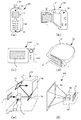
半導体などの物質の結晶成長を構成元素の異なる下地層上で行うと、格子定数などの構造パラメータの違いから固有の構造とは異なる半導体が得られることが知られている。結晶成長の方法としてはこれまで分子線エピタキシー法やCVD法などの手法が用いられてきた。これらの従来法は、図7に示したように、下地層101上に精密に原子層102〜104を1層ごと(レイヤー−バイ−レイヤー)に堆積させる方法である。
【0003】
【発明が解決しようとする課題】
しかしながら、これら従来の結晶成長の手法では原子層を1層ごと堆積させるため、結晶成長に時間を要する。また、結晶成長面に不純物が混入すると結晶成長が阻害されるため10-9Torrという超高真空を必要とし、装置構成が複雑になるという欠点がある。
【0004】
そこで、本発明の第1の目的は格子定数などの構造パラメータが異なる下地層上で複数の半導体を含む積層体を容易に結晶化あるいは結晶成長をさせる方法を提供することである。
【0005】
本発明の第2の目的はキャリア移動度などの電子物性に優れた性能を有する電界効果型トランジスタなどの半導体素子を提供することである。
【0006】
本発明の第3の目的は電子物性に優れた性能を有する、本発明の製造方法で製造された半導体素子を備える電子機器を提供することである。
【0007】
【課題を解決するための手段】
上記第1の目的を達成するために、第1の発明に係る半導体積層体の製造方法は、第1の半導体層の上に形成された第2の半導体層に対して光照射を行うことにより第2の半導体層の少なくとも一部分の構造変化を誘起する工程を備える。すなわち、第2の半導体層は第1の半導体層上に形成されているので、第2の半導体層の構造変化が下地層である第1の半導体層の影響を受けやすくなる。
【0008】
なお、第1の発明に係る半導体積層体の製造方法には、厳密に第2の半導体層のみに光照射を行う場合の他、第2の半導体層を通して第1の半導体層に対して光照射を行う場合をも含む。
【0009】
ここで、本明細書全てを通して、上記の「半導体積層体」とは少なくとも2つの半導体層を含む積層体を意味し、第1の半導体層の下に他の物質層が存在するものに関しても本発明の適用範囲である。また、第2の半導体層上に他の物質層が存在しているものに関しても、本発明の適用範囲である。
【0010】
また、「構造変化」とは微視的には反応や格子欠陥生成など、巨視的には溶融、結晶化または再結晶化などの、光照射により誘起される一般的な現象を意味するものである。また、この「構造変化」は必ずしも一つの現象のみからなるものではなく、複数の現象を含むこともある。例えば、溶融の後に結晶化する一連の物質の変化も、本明細書を通して、「構造変化」と定義する。
【0011】
また、第1の発明に係る半導体積層体の製造方法は、上記の半導体積層体の製造方法において、構造変化を第1の半導体層の影響を受けるように誘起する。第2の半導体層の光照射による構造変化は第1の半導体層の影響を受けるため、対応する単層半導体に対する光照射により誘起される構造変化とは異なるものとなりやすい。
【0012】
なお、ここで、第1の半導体層の構造変化に対する影響とは、第1の半導体層の構造、格子定数、比熱、キャリア移動度、電子供与能、電子受容能、または第1の半導体層を構成する元素の第2の半導体層を構成する元素に対する化学的親和性などの影響により、第2の半導体層の結晶化、溶融、格子欠陥生成または反応などが、第2の半導体層固有あるいは対応する単層半導体の構造変化とは異なることを意味している。さらに、第1の半導体層の影響により構造変化により形成された領域の物質構造も第1の半導体層の影響を受けたものとなりやすい。このことは、はX線回折構造解析法、電子線回折構造解析法、中性子線回折構造解析法、赤外振動分光法、またはラマン振動分光法などの種々の構造解析的手段で調べることができる。また、物質構造はキャリア移動度または光電変換効率などの光電子物性にも反映されるので、光電物性を調べることでも推定できる。
【0013】
第2の発明に係る半導体積層体の製造方法は、第1の半導体層の上に形成された第2の半導体層に対して光照射を行うことにより第2の半導体層の少なくとも一部分を結晶化させる工程を備える。これにより、結晶化の際に第1の半導体層の影響を受け、第2の半導体層固有の結晶構造とは異なる結晶構造を有する領域を第2の半導体層に形成することが可能となる。なお、ここで、本明細書を通して、「結晶化」とは、非晶質から結晶化するのみを意味するのではなく、多結晶状態または単結晶状態から結晶化することをも含む。
【0014】
本発明の半導体積層体の製造方法は、第2の発明の半導体積層体の製造方法において、結晶化を第1の半導体層の影響を受けるように行う。これにより第2の半導体層固有あるいは対応する単層半導体の結晶構造とは異なる結晶構造を有する領域を第2の半導体層に形成することができるようになる。
【0015】
本発明に係る半導体積層体の製造方法は、上記のいずれかに記載の半導体積層体の製造方法において、結晶性領域を有する半導体層を、第1の半導体層として用いる。第1の半導体層に存在する結晶性領域の規則的な物質構造は、第2の半導体層における構造変化、特に結晶化の際に摂動を与えやすい。
【0016】
本発明に係る半導体積層体の製造方法は、上記のいずれかに記載の半導体積層体の製造方法において、単結晶からなる半導体層を、第1の半導体層として用いる。すなわち、第2の半導体層における結晶化などの構造変化の際に、単結晶からなる第1の半導体層の規則的な物質構造による摂動を受けやすくなる。
【0017】
本発明に係る半導体積層体の製造方法は、上記のいずれかに記載の半導体積層体の製造方法において、非晶質領域を有するように形成された半導体層を、第2の半導体層として用いる。非晶質領域を有するような半導体層は、結晶性を有する半導体層に比べて、比較的容易かつ短時間で形成することができるという利点を有する。
【0018】
本発明に係る半導体積層体の製造方法は、上記のいずれかに記載の半導体積層体の製造方法において、第1の半導体層の光照射による溶融挙動とは異なる溶融挙動を示す半導体層を、第2の半導体層として用いる。
【0019】
ここで、「溶融挙動が異なる」とは溶融する最低温度や溶融状態における粘性、溶融に要する光エネルギーまたは熱エネルギーなどを意味するが、このため、第1の半導体層または第2の半導体層のいずれかのみを選択的に溶融させることができる。
【0020】
本発明に係る半導体積層体の製造方法は、上記のいずれかに記載の半導体積層体の製造方法において、第1の半導体層の最低溶融温度より低い最低溶融温度を有する半導体層を、第2の半導体層として用いる。これにより第2の半導体層のみを溶融させることができる。
【0021】
本発明に係る発明は、上記のいずれかに記載の半導体積層体の製造方法において、第1の半導体層の溶融に要する光エネルギーより低い光エネルギーで溶融する半導体層を、第2の半導体層として用いる。これにより、第2の半導体層のみを溶融させることができる。
【0022】
本発明に係る半導体積層体の製造方法は、上記のいずれかに記載の半導体積層体の製造方法において、第1の半導体層の組成とは異なる組成を有する半導体層を、第2の半導体層として用いる。このような例として第1の半導体層及び第2の半導体層が、それぞれゲルマニウム及びシリコンからなる場合が挙げられる。このような場合、結合長や格子定数などの物質パラメーターが、第1の半導体層と第2の半導体層とでは異なるため、第2の半導体層の構造変化や結晶化の際、第2の半導体層をなすシリコン固有の結晶構造が第1の半導体層をなすゲルマニウムの影響を受けやすくなり、このことは物性面にも反映されることになる。
【0023】
本発明に係る半導体積層体の製造方法は、上記のいずれかに記載の半導体積層体の製造方法において、シリコン、ゲルマニウム、及びシリコンとゲルマニウムとを含む複合材料のうちから選ばれる2つの材料を、第1の半導体層及び第2の半導体層の材料として用いる。上記の3つの材料はいずれも、形成方法が確立しており、また、互いに類似の構造パラメータを有しているので、光照射前の積層体の形成が比較的容易であるという利点を有する。
【0024】
本発明に係る半導体積層体の製造方法は、上記のいずれかに記載の半導体積層体の製造方法において、100nm以下の膜厚を有する半導体層を第2の半導体層として用いる。これにより第2の半導体層を深さ方向に均一に光励起しやすくなる。
【0025】
本発明に係る半導体積層体の製造方法は、上記のいずれかに記載の半導体積層体の製造方法において、500ns以下のパルス幅を有する光を光照射に用いる。この方法によれば、用いる光のパルス幅が十分に短いため、光照射の際に発生する熱の第1の半導体層方向への拡散が抑制され、第2の半導体層のみの構造変化を誘起することが可能になるという利点を有する。
【0026】
本発明に係る半導体積層体の製造方法は、上記のいずれかに記載の半導体積層体の製造方法において、波長が600nm以下である光を光照射に用いる。これにより第2の半導体層を効率良く光励起することができる。
【0027】
本発明に係る半導体素子は、基板上に形成された第1の半導体層と、該第1の半導体層上に形成された第2の半導体層とを備える半導体素子であって、前記第1の半導体層と前記第2の半導体層とは異なる格子定数をもつ材料からなり、前記第1の半導体層は結晶領域を有し、前記第2の半導体層は該第2の半導体層固有の結晶構造とは異なる結晶構造であるひずみ結晶を有することを特徴とする。
【0028】
第3の発明に係る半導体素子は、第2の発明の半導体積層体の製造方法により製造される半導体積層体の第2の半導体層のうち少なくとも結晶化領域が半導体素子の能動領域として用いられる。この結晶化領域における物質構造は第1の半導体層の構造や物性による摂動を受けやすく、第2の半導体層を構成する材料の固有の構造や物性とは異なるものとなりやすい。したがって、この半導体素子は優れた素子として機能することが可能である。なお、本明細書を通して、能動領域とはキャリアが流れる少なくとも1つの部位または1つの領域を意味しており、例えば半導体素子がMOSトランジスタである場合は、能動領域とはソース領域、ドレイン領域またはチャンネル領域のうち少なくとも1つの領域を指している。
【0029】
本発明に係る半導体素子は、シリコンとゲルマニウムとを含む複合半導体材料からなる第1の半導体層上に第2の半導体層として形成されたシリコン層に対する光照射により形成された結晶化領域が半導体素子の能動領域として用いられる。シリコンとゲルマニウムとを含む複合半導体の物質構造とシリコンの物質構造との適当な構造の不一致のため、積層体を形成しやすく、かつまた、シリコン層に対する光照射による結晶化領域の際に第1の半導体層の摂動も受けやすい。これにより、この半導体素子は通常のシリコンを能動領域に用いた従来の半導体素子に比べて、優れた性能を発揮しやすい。
【0030】
本発明に係る半導体素子は、上記の半導体素子において、前記結晶化領域の物質構造がシリコン結晶固有の物質構造とは異なっている。この半導体素子は従来法で形成されたシリコンに比べてキャリア移動度などの点で優れた特性を発揮しやすい。
【0031】
本発明の半導体素子は、上記のいずれかに記載の半導体素子において、半導体素子が電界効果型トランジスタである。これによりキャリア移動度などの点で優れた電界効果トランジスタが実現される。
【0032】
第4の発明の積層体の製造方法は、第1の物質層の上に形成された第2の物質層に対する光照射により第2の物質層の構造変化を誘起する。第2の物質の例としてはセレンやテルルなどに代表されるカルコゲン類の酸化物が挙げられるが、これに限定されることなく、結晶可能な物質であれば本発明を適用可能である。
【0033】
本発明の積層体の製造方法は、上記の積層体の製造方法において、第1の物質層の影響を受けるように、構造変化をさせる。これにより物質固有の構造とは異なった構造を有する領域を形成することができる。この形成領域は様々な素子に用いることができる。
【0034】
第5の発明に係る半導体積層体の製造方法は、基板上に、第1の半導体、または第1および第2の半導体を含む第1の半導体層を形成する工程と、第1の半導体層上に第2の半導体からなる第2の半導体層を形成する工程と、第1の半導体層および第2の半導体層からなる積層体に光照射を行い、構造変化を誘起する工程と、を備える。
【0035】
ここで「構造変化」とは、前述した定義に加え、構成原子の結合状態が変化することを意味し、例えば非晶質の結晶化や、多結晶質の再結晶化や結晶状態の変化等をも指す。
【0036】
本発明の半導体積層体の製造方法は、上記の半導体積層体の製造方法において、第1の半導体はゲルマニウムである。
【0037】
本発明の半導体積層体の製造方法は、上記の半導体積層体の製造方法において、第2の半導体はシリコンである。
【0038】
本発明の半導体積層体の製造方法は、上記いずれかに記載の半導体積層体の製造方法において、第1の半導体層の形成と第2の半導体層の形成は真空中で連続して行う。
【0039】
本発明の半導体積層体の製造方法は、上記いずれかに記載の半導体積層体の製造方法において、第1の半導体層は結晶性領域を含む。
【0040】
本発明の半導体積層体の製造方法は、上記いずれかに記載の半導体積層体の製造方法において、第1の半導体層は光照射による結晶化により形成されたものである。
【0041】
本発明の半導体積層体の製造方法は、上記の半導体積層体の製造方法において、第1の半導体層は複数回の光照射による結晶化により形成されたものである。
【0042】
本発明の半導体積層体の製造方法は、上記の半導体積層体の製造方法において、第1の半導体層への光照射は真空中で行われる。
【0043】
本発明の半導体積層体の製造方法は、請求項1乃至8のいずれかに記載の半導体積層体の製造方法において、積層体への光照射は少なくとも第2の半導体層を完全溶融させるエネルギー密度以上の強度により行われる。
【0044】
本発明の半導体積層体の製造方法は、上記いずれかに記載の半導体積層体の製造方法において、第2の半導体層の膜厚は50nm以下である。
【0045】
本発明の半導体積層体の製造方法は、上記いずれかに記載の半導体積層体の製造方法において、光照射はパルス幅が500ns以下のパルスレーザーを用いて行う。
【0046】
本発明の半導体積層体の製造方法は、上記いずれかに記載の半導体積層体の製造方法において、光照射は波長が600nm以下のパルスレーザーを用いて行う。
【0047】
第6の発明は、上記いずれかに記載の半導体積層体の製造方法により製造された半導体素子である。これら半導体素子の結晶化領域における物質構造は第1の半導体層の構造や物性による摂動を受けやすく、第2の半導体層を構成する材料の固有の構造や物性とは異なるものとなりやすい。したがって、この半導体素子は優れた素子として機能することが可能である。
【0048】
第7の発明は、第6の発明の半導体素子を備える電子機器である。
【0049】
ここで「電子機器」には限定が無いが、本発明の半導体素子、例えばTFTで構成された表示装置等を備えるものが考えられる。このような電子機器として、例えば、携帯電話、ビデオカメラ、パーソナルコンピュータ、ヘッドマウントディスプレイ、リア型またはフロント型のプロジェクター、さらに表示機能付きファックス装置、デジタルカメラのファインダ、携帯型TV、DSP装置、PDA、電子手帳等が挙げられる。
【0050】
【発明の実施の形態】
以下、本発明の実施の形態を図面に基づいて詳述する。
(実施形態1)
本発明の実施形態は、第1の半導体層の上に形成された第2の半導体層に対して光照射を行うことにより第2の半導体層の少なくとも一部分に構造変化を誘起させる積層体の製造方法に関する。
【0051】
図1に、本実施形態の積層体の製造方法における製造工程断面図を示す。
【0052】
まず、図1(ST1)に示すように、第1の半導体層201の上に第2の半導体層202を形成する。これら第1及び第2の半導体層に用いる半導体としてはシリコン(Si)やゲルマニウム(Ge)等の14族のみからなる半導体結晶、シリコン・ゲルマニウム(SixGe1−x:0<x<1)結晶やシリコン・カーバイド(SixC1−x:0<x<1)結晶やゲルマニウム・カーバイド(GexC1−x:0<x<1)などの14族元素を含む複合半導体結晶、ガリウム・ヒ素(GaAs)やインジウム・アンチモン(InSb)などの13族元素と15族元素との化合物半導体、またはカドミウム・セレン(CdSe)等の12族元素と16族元素との化合物半導体、あるいはシリコン・ゲルマニウム・ガリウム・ヒ素(SiwGexGayAsz:w+x+y+z=1)などのさらなる多元系化合物半導体やこれらの半導体にリン(P)、ヒ素(As)、及びアンチモン(Sb)などのドナー元素を添加したN型半導体、もしくはホウ素(B)、アルミニウム(Al)、ガリウム(Ga)、及びインジウム(In)などのアクセプター元素を添加したP型半導体も挙げられる。また、第1および第2の半導体層を構成する材料としては上記の材料を任意に組み合わせることが可能である。
【0053】
第1の半導体層は単結晶構造をとっていること好ましい。こ単結晶の構造としては、単結晶基板そのものを用いるか、あるいは単結晶基板上にエピタキシャル成長により形成した半導体単結晶を用いることができる。実用上のコストを考慮すると、シリコン基板上に固相エピタキシャル成長あるいは分子線エピタキシーにより成長させたひずみ緩和シリコンゲルマニウムを第1の半導体層として用いるのが好ましい。
【0054】
本発明では、第1の半導体層の最低溶融温度は第2の半導体層の最低溶融温度より高いことが好ましい。このように溶融温度を設定するには、例えば第1の半導体層としてはシリコンとゲルマニウムとの組成比が0.5:0.5またはシリコンが0.5以上の割合で含まれたもの、第2の半導体層としてはアモルファスシリコンという組み合わせが好ましい。
【0055】
第1の半導体層201上に第2の半導体層202を形成する場合には界面状態が結晶成長に大きく影響するため、第1の半導体層上にある金属、有機物などを酸、アルカリ溶液、または酸素プラズマによる前処理を施すことが、デバイスの歩留まりの向上ためには好ましい。更に第1の半導体層上の自然酸化膜を除去した直後に第2の半導体層202を形成することが好ましい。
【0056】
第1の半導体層201の上に第2の半導体層202を形成する方法としては、例えばAPCVD法、LPCVD法及びPECVD法などのCVD法、あるいはスパッタ法や蒸着法などのPVD法で形成することができる。
【0057】
第2の半導体層202としてシリコン膜を用いる場合、LPCVD法では例えば基板温度を400℃程度から700℃程度として、ジシラン(Si2H6)などを原料に用い、堆積し得る。PECVD法では例えば基板温度が100℃程度から500℃程度として、モノシラン(SiH4)などを原料に用い、堆積可能である。
【0058】
スパッタ法を用いる場合には例えば基板温度は室温から400℃程度である。スパッタ法により2種類以上の元素を含む半導体層(例えばシリコンゲルマニウムSixGe1−x :0<x<1など)を堆積させる場合、ターゲットとして所望の組成を有する原料を用いることによって、形成される半導体層の組成もほぼ同じになり、且つ有毒なガスを用いる必要が無い点において優れている。
【0059】
本発明にあっては第1の半導体層201の上に形成された第2の半導体層202の初期状態(as−deposited状態)は非晶質、混晶質、微結晶質、または多結晶質等のいずれの状態であっても構わないが、特に先に述べたように第2の半導体層の方が融点が低くなる条件を満たすために、非晶質であることが好ましい。
【0060】
なお、本明細書中では非晶質の結晶化のみならず、多結晶質や微結晶質の再結晶化をも含めてすべて結晶成長、結晶化と呼ぶ。第2の半導体層の厚さは、特に限定されないが、後述するように光照射により全体を溶融させることができること、及びひずみ結晶成長が維持できることの両方を満たす膜厚100nm以下が好ましい。通常、LPCVD法、PECVD法等のCVD法およびスパッタリングで堆積させた半導体表面は自然酸化膜で覆われていることが多い。このため、光を照射する前にこの自然酸化膜を除去することが好ましい。このためには例えばフッ酸溶液に浸してウエットエッチングする方法や、フッ素ガスを含んだプラズマ中におけるドライエッチングを採用することができる。
【0061】
次に、図1(ST2)に示すように、第2の半導体層202を形成した基板を石英の窓204を有する光照射用真空チャンバー203内に設置する。光照射用真空チャンバー203を真空に排気した後この石英窓204を通して光205を照射し、第2の半導体層202の光結晶化を行う。光結晶化の際に半導体層に雰囲気中から混入する不純物量を真空排気することによって低減させることができる。光照射により不純物が混入しやすい第2の半導体層202の表面は、特に電界効果トランジスタの形成を意図した場合、最も重要なMOS界面を形成するため、不純物の混入を抑えることが素子性能およびそのばらつきを良好に制御する点で好ましい。
【0062】
ここで光照射に用いる光源について説明する。光源としては、例えば、低圧水銀ランプ、高圧水銀ランプ、超高圧水銀ランプ、亜鉛ランプ、ハロゲンランプ、エキシマランプ及びキセノンランプが挙げられる。また、エキシマレーザー、アルゴンイオンレーザー、クリプトンイオンレーザー、Nd:YVO4レーザー、Nd:YAGレーザー、Nd:YLFレーザー、Ti:サファイアレーザー、半導体レーザー、色素レーザーなどのレーザーの基本波及び上記のレーザーの基本波の非線型光学効果により得られる光を用いることもできる。
【0063】
本発明においては、照射光が半導体層(特に第2の半導体層202)において強く吸収されることが好ましい。このため、この照射光としては紫外域また
はその近傍の波長を持つエキシマレーザー、アルゴンイオンレーザー、Nd:YAGレーザーの高調波などの光を用いることが特に好ましい。特に第2の半導体層の膜厚が小さい場合、波長の短いエキシマレーザーが光源として適しており、逆に膜厚が大さい場合は波長の長いNd:YAGレーザーの第2高調波が光源として適しているが、おおむね波長が600nm以下のレーザー光が上記の条件を満たしている。
【0064】
次にこれらのレーザー光の照射方法について述べる。レーザー光照射は半導体層(201、202)の温度を例えば室温(25℃)程度から400℃程度の間として、背景真空度が例えば10-4Torr程度から10-9Torr程度の真空中にて行う。レーザー照射の一回の照射面積は例えば対角5mm程度から100mm程度の正方形または長方形状とする。なお、照射面積はフライアイレンズなどを用いた光学系により、レーザー照射領域の大きさは適宜制御することができる。
【0065】
第2の半導体層に対してパルスレーザーを用いて光照射を行うと、第2の半導体層202の光照射された領域に対応して吸収された光エネルギーにより熱が発生し、ごく短時間に温度上昇が起こる。レーザーのパルス幅は500ns以下が好ましい。その際発生した熱が拡散するため、第2の半導体層は短時間で冷却される。光205の照射エネルギーが第2の半導体層を溶融するのに十分な場合には、第2の半導体層は溶融領域206し、冷却過程において結晶化する。照射エネルギー密度を増加させると、第2の半導体層の深い部分まで溶融領域206となり、あるエネルギー以上では完全溶融する。さらにレーザー光のエネルギー密度を増加させると第1の半導体層も溶融することになる。
【0066】
すなわち、第2の半導体層が部分的にしか溶融しないようなエネルギー密度での光照射の場合、第2の半導体層は任意の場所での結晶核発生およびこれを核とした結晶化が起こるため、多結晶となりやすい。一方、第2の半導体層が完全に溶融し、且つ、第1の半導体層が溶融しないような光照射の条件下では、溶融状態にある第2の半導体層は第1の半導体層の結晶を種としたエピタキシャル成長をする。このとき結晶化の結晶化速度が毎秒1〜10mに達する超高速結晶成長となる。特に本発明の結晶化法の優れているところは、従来のレイヤー・バイ・レイヤーの結晶化に比べて、高速で欠陥の少ないひずみ結晶が得られることである。
【0067】
基板を相対的に移動させながら、このような光照射を繰り返すことによって、8インチ以上の大面積基板領域全体に、短時間でひずみ結晶を形成することができるのである。また、第2の半導体層の表面への最低限の不純物混入を回避すればよいだけなので、結晶成長に必要な真空度はたかだか10-6Torr程度であり、従来の結晶化法のような超高真空装置は必要とせず、製造コストも低くおさえることができるのである。さらに本発明に係る結晶化法では、臨界膜厚を飛躍的に増大させることができるという特徴がある。例えば混合比が0.5:0.5のひずみ緩和シリコンゲルマニウム結晶上にシリコン100%の第2の半導体を形成してパルスレーザーを用いて光照射を行うと、従来の方法では不可能であった10nm以上のエピタキシャル成長したひずみシリコン結晶を実現することができる。第2の半導体層の下地層である第1の半導体層との大きな格子ミスマッチために、光照射により形成されたシリコン結晶は強烈な格子ひずみを有することになり、これによって、従来法では実現不可能であった強い移動度エンハンスメントを有する半導体を得ることが可能となる。
【0068】
照射光のエネルギー密度が第2の半導体層を完全溶融させ、かつ、第1の半導体層を溶融させないような条件に設定すると、上述のようにひずみ結晶のエピタキシャル結晶化が可能となる。第1の半導体層は固体、第2の半導体層は液体の状態から結晶成長が開始し、しかもこれが10-9秒のオーダーのごく短時間に終了するため、結晶化中に原子同士の交換がほとんど起こらない。すなわち従来技術で問題であると指摘した第1の半導体層と第2の半導体層との境界でのミキシングがほとんど起こらないのである。このような条件を実現するためには、第2の半導体層の融点は第1の半導体層の融点より低いことが望ましい。一般的には同じ材料でも非晶質は結晶より融点が低くなるので、第1の半導体層は結晶、第2の半導体層を非晶質とし、これに光照射を行うことにより、ひずみ結晶化が実現しやすい。
【0069】
一方、第2の半導体層のみでなく、第1の半導体層も一部溶融させるようなエネルギー密度の光を照射した場合、第2の半導体層に加えて、第1の半導体層には第2の半導体層側に溶融領域が形成され、第2の半導体層と第1の半導体層との境界が溶融状態になるため、相互拡散が起こる。結晶化は第1の半導体層の溶融領域から始まり、これに第2の半導体層の結晶化が追従するが、この第2の半導体層の結晶化は第1の半導体層の影響を受けやすく、ひずみ結晶が得られることになる。
【0070】
以上のように、少なくとも第2の半導体層を完全溶融させるのに十分なエネルギー密度をもった光照射を行うことにより、良質なひずみ結晶がかつ大面積に形成することが可能となる。
【0071】
本実施形態の方法で形成したひずみ半導体は、移動度のエンハンスメントが起こるので、電流駆動能力が高く、半導体素子として極めて優れた性能を発揮する。特にひずみシリコンを能動層あるいは能動領域として用いる電界効果トランジスタが実用上重要である。特に第1の半導体にひずみ緩和シリコンゲルマニウム結晶を、第2の半導体にシリコンを用い、前述の結晶化方法により製造したひずみシリコン結晶を、従来用いられている熱酸化法により酸化することで、界面準位の少ない良好なゲート絶縁膜を形成することができるからである。これにゲート電極、ソース、及びドレイン電極などを形成して電界効果トランジスタを製造すると、移動度が2倍も高いトランジスタが実現できるのである。現在の半導体産業では、素子サイズが1μm以下となり、配線容量が回路のスピードを律速している。このような状況下でデザインルールを変えなくとも電流駆動能力の高い本発明が開示するひずみシリコンを用いることにより、2世代分の微細化技術開発に相当するような高性能化を容易に実現することができる。
【0072】
【第1実施例】
本実施形態1に沿った第1実施例を、図2を参照して説明する。
【0073】
まず、図2(ST1)に示すように、ここでは基板の一例として直径8インチの丸型、P型で100面方位、比抵抗3〜5Ωcmのシリコン基板301を用いた。このシリコン基板をRCA洗浄によりクリーニングし、水素終端により安定した基板表面を調整した。しかる後、この基板を真空容器内に保持し、基板温度100℃で第1の半導体層となるシリコンゲルマニウム膜302(Si0.7Ge0.3、膜厚:250nm)を分子線エピタキシーにより形成した。この膜厚は臨界膜厚以上のため基板近くで応力緩和がおこり、ひずみ緩和シリコンゲルマニウム結晶が形成された。しかる後、この第1の半導体層上に減圧CVD(LPCVD)によりアモルファスシリコン膜303を50nmの厚さに形成した。本実施例では高真空型LPCVD装置を用いて、原料ガスのジシラン(Si2H6)を200SCCM流し、425℃の堆積温度で非晶質シリコン膜303を堆積した。まず高真空型LPCVD装置の反応室を250℃とした状態で反応室の内部に複数枚(例えば17枚)の基板の表側を下向きとして配置した。次にターボ分子ポンプの運転を開始し、ターボ分子ポンプが定常回転に達した後、反応室内の温度を約1時間掛けて250℃から425℃の堆積温度まで上昇させた。昇温開始後の最初の10分間は反応室にガスを全く導入せず真空中で昇温を行ない、しかる後99.9999%以上の純度の窒素ガスを300SCCM流し続けた。この時の反応室内における平衡圧力は、3.0×10-3Torrであった。堆積温度に到達した後、原料ガスであるジシラン(Si2H6)を200SCCM流すと共に、純度が99.9999%以上の希釈用ヘリウム(He)を1000SCCM流した。堆積開始直後の反応室内圧力はおよそ0.85Torrであった。堆積の進行と共に反応室内の圧力は徐々に上昇し、堆積終了直前の圧力は凡そ1.25Torrとなった。堆積したシリコン膜303は基板の周辺部約7mmを除いた8インチ基板の領域内において、その膜厚変動は±5%以内であった。
【0074】
次に、図2(ST2)に示すように、この基板を光照射用真空チャンバ304にセットし10-7Torr程度まで真空排気し、石英窓305を通して波長308nmのXeClエキシマレーザーを用いて光306の照射を行った。もちいたレーザーの光はパルス幅が25nsで、フライアイレンズを用いた光学系を通して試料面でのビームサイズが10mm×10mmの正方形で強度分布が5%以内のトップフラットビームに整形して照射した。エネルギー密度は450mJ/cm2として、一ヶ所あたり1パルスの光を照射した。照射領域はデバイスの1チップと同等サイズとなっており、それぞれのチップ位置に相当する場所を同様に10mm×10mmのビームで1パルスの光を照射し、基板を動かしながら8インチ基板全面に光照射を行った。これにより、光照射を行った各10mm×10mmのエリアに溶融領域307が形成された。その後、図2(ST3)に示すように、ひずみ緩和シリコンゲルマニウム結晶上にひずみシリコン結晶領域308を形成することができた。
【0075】
その後、毎分10℃のレートで炉内温度を上昇させ、1160℃に達した後、この温度で10分間熱酸化を行った。その後炉内温度は1160℃に維持したままでガスを窒素に切り替え、更に15分の熱処理を行った。この後毎分5℃の降温レートで冷却し、800℃になったら基板を取り出した。このようにして形成したゲート酸化膜309は膜厚が60nmで、界面順位密度が1010cm− 2の極めて良好な界面特性を示した。
【0076】
次に、図2(ST4)に示すように、ゲート電極310を、多結晶シリコンを用いて形成し、層間絶縁膜311をTEOSと酸素混合によるプラズマCVDにて形成し、コンタクトホールを開けた後、ソース及びドレイン電極312を形成して、電界効果トランジスタを完成させた。
【0077】
このような方法により製造した電界効果型トランジスタは、従来のひずみシリコンを用いない場合より2倍も高い電界効果移動度を示した。これは本発明が開示するレーザー光照射を用いた超高速結晶成長により製造したひずみシリコンを用いたことにより初めて実現できたものである。
(実施形態2)
本発明の実施形態2は、実施形態1のように積層体の上層である第2の半導体層のみでなく、第1の半導体層および第2の半導体層からなる積層体に光照射を行う積層体の製造方法に関する。
【0078】
図1に、本実施形態の積層体の製造方法の製造工程断面図を示す。
【0079】
本願発明の実施のためには、図3(ST1)に示すように、基板400上に第1の半導体層401、更にその上に第2の半導体層402を形成する。本発明を適応し得る基板400としては金属等の導電性物質、シリコン・カーバイト(SiC)やアルミナ(Al2O3)や窒化アルミニウム(AlN)等のセラミック材料、溶融石英やガラス等の透明または非透明絶縁性物質、シリコンウェーハー等の半導体物質、並びにそれを加工したLSI基板等が可能である。更にはPESやPET等のポリマーも基板として用いることが可能である。
【0080】
なお、図3(ST1)では基板上に直接半導体層401、402を形成する場合を示しているが、半導体層401、402は基板上に直接又は下地保護膜や下部電極等を介して堆積するが、ガラスやポリマー基板上に半導体層を形成する場合には下地保護膜が必要となる。下地保護膜を形成する場合は酸化硅素膜(SiOX:0<x≦2)や窒化硅素膜(Si3Nx:0<x≦4)等の絶縁性物質が用いられる。薄膜トランジスタ(TFT)などの薄膜半導体装置を通常のガラス基板やポリマー上に作成する場合、半導体膜への不純物制御が重要である。この場合、ガラス基板やポリマー基板中に含まれているナトリウム(Na)等の可動イオンが半導体膜中に混入しない様に下地保護膜を形成した後に半導体膜を堆積する事が好ましい。同じ事情は各種セラミック材料を基板として用いる場合にも通ずる。下地保護膜はセラミック中に添加されている焼結助材原料などの不純物が半導体部に拡散及び混入するのを防止するのである。金属材料などの導電性材料を基板として用い、且つ半導体膜が金属基板と電気的に絶縁されていなければならない場合には、絶縁性を確保する為に当然下地保護膜は必要不可欠である。更に半導体基板やLSI素子上に半導体膜を形成する時にはトランジスタ間や配線間の層間絶縁膜が同時に下地保護膜でもある。
【0081】
下地保護膜は、まず基板を純水あるいはアルコールなどの有機溶剤で洗浄した後、常圧化学気相堆積法(APCVD法)や低圧化学気相堆積法(LPCVD法)、プラズマ化学気相堆積法(PECVD法)等のCVD法或いはスパッター法等で形成する。
下地保護膜として酸化硅素膜を用いる場合、常圧化学気相堆積法では基板温度を250℃程度から450℃程度としてモノシラン(SiH4)や酸素を原料として堆積し得る。
【0082】
プラズマ化学気相堆積法やスパッター法では基板温度は室温から400℃程度である。下地保護膜の膜厚は基板からの不純物元素の拡散と混入を防ぐのに十分な厚さが必要で、その値は最小で100nm程度以上である。ロット間や基板間のばらつきを考慮すると200nm程度以上が好ましく、300nm程度あれば保護膜としての機能を十分に果たし得る。下地保護膜がIC素子間やこれらを結ぶ配線等の層間絶縁膜を兼ねる場合には、通常400nmから600nm程度の膜厚となる。絶縁膜が余りにも厚くなると絶縁膜のストレスに起因するクラックが生ずる。その為最大膜厚は2μm程度が好ましい。生産性を考慮する必要が強い場合、絶縁膜厚は1μm程度以下であることが好ましい。
【0083】
次に上記基板400上に第1の半導体層401を形成する。この半導体層は第1の半導体、または第1および第2の半導体から構成される。本発明を適応し得る第1および第2の半導体としてはシリコン(Si)やゲルマニウム(Ge)等の四族単体の半導体の他に、シリコン・ゲルマニウム混合物(SixGe1−x:0<x<1)やシリコン・カーバイド(SixC1−x:0<x<1)やゲルマニウム・カーバイド(GexC1−x:0<x<1)等の四族元素複合体の半導体、ガリウム・ヒ素(GaAs)やインジウム・アンチモン(InSb)等の三族元素と五族元素との複合体化合物半導体、またはカドミウム・セレン(CdSe)等の二族元素と六族元素との複合体化合物半導体等がある。或いはシリコン・ゲルマニウム・ガリウム・ヒ素(SixGeyGazAsz:x+y+z=1)と云った更なる複合化合物半導体やこれらの半導体にリン(P)、ヒ素(As)、アンチモン(Sb)などのドナー元素を添加したN型半導体、或いはホウ素(B)、アルミニウム(Al)、ガリウム(Ga)、インジウム(In)等のアクセプター元素を添加したP型半導体に対しても本発明は適応可能であり、第1および第2の半導体は上記材料を任意に組み合わせることが可能である。
【0084】
しかしながら、材料の扱いやすさ、格子マッチングを考えると、シリコンおよびゲルマニウムが最も適している。純粋なシリコンとゲルマニウムの結晶は共にダイヤモンド構造で4.2%の格子ミスマッチがある。互いの混合比を変えてシリコンとゲルマニウム混合物の結晶を形成することにより、この混合物の格子定数を制御できることがこれら材料の利点の一つである。すなわち、第1の半導体としてゲルマニウムを、第2の半導体としてシリコンを用いた場合、例えばそれぞれ50%の割合で混合すると純粋なシリコンとゲルマニウムの丁度中間の格子定数を持つ結晶が作製できるのである。また、お互い全率固溶であるため後述する光照射を利用した熱作用による結晶化に際して偏析がおこらないという利点を有する。以上の理由により、第1および第2の半導体としてはシリコンとゲルマニウムが適している。もちろん、ここで第1の半導体層としてゲルマニウム単体を用いることも可能である。
【0085】
本実施形態2の第1の半導体層形成に適用しうる成膜方法としては、常圧化学気相堆積法(APCVD法)や低圧化学気相堆積法(LPCVD法)、プラズマ化学気相堆積法(PECVD法)超高真空CVD法等のCVD法或いはスパッター法、または電子ビーム蒸着などの真空蒸着法等がある。
【0086】
CVD法ではSiH4やGeH4のガスを原料として成膜が可能であり、スパッター法や蒸着法ではSiやGeの固体ターゲットを原料として用いることができる。スパッター法は堆積させる半導体が2種類以上の材料の混合物(例えばシリコンゲルマニウムSixGe1−x:0<x<1等)の場合、ターゲットにそのような組成のものを用いれば、形成された半導体の組成もほぼ同じになり、且つ有毒なガスを用いる必要が無い点において優れている。
【0087】
本発明の第1の半導体層は結晶領域を有することが好ましい。これは後述する第2の半導体層に格子ミスマッチによるひずみを持たせる必要があるからである。従って、上述した半導体層形成方法を用いた場合、成膜時の基板温度を少なくとも600℃以上に上げる必要が生じる。このため安価なガラスやポリマーなどの基板には適さない。さらに有効な方法は、基板上に第1の半導体層を低温で形成し、しかる後に第1の半導体層を光照射によって多結晶化させることである。低温で形成した第1の半導体層はほとんどの場合非晶質となる。これに例えばパルスレーザーなどを照射することによってごく短時間で多結晶化を行うことができ、この方法ならば下地保護膜を用いることでガラスやポリマー基板にも本発明の薄膜半導体の製造方法を適用しうる。
【0088】
第1の半導体層への不純物の混入を避ける目的と、引き続いて形成される第2の半導体層との界面を清浄に保つ目的で、この光照射は真空中で行うのが望ましい。特に第2の半導体層と第1の半導体層との界面に不純物が存在すると、第2の半導体層のひずみ結晶成長を行う際に結晶欠陥(積層欠陥、転移)の発生原因となり第2の半導体層の結晶性を著しく損なう場合がある。
【0089】
次に、第1の半導体層401上に第2の半導体層402を形成する。第1の半導体層を形成した後、これを大気にさらした場合には第1の半導体層401上にある金属、有機物などを酸、アルカリ溶液により除去するか、あるいは酸素プラズマによりアッシングすることが重要である。更に第1の半導体層401上の自然酸化膜を除去し、直後に第2の半導体層402を形成する必要がある。更に望ましくは、先に述べたように第1の半導体層を形成した後、真空中連続で第2の半導体層を形成する。第2の半導体層の材料としては、第1の半導体層を構成する半導体としては、異なる格子定数を持つ材料であれば適用可能である。しかし、第1の半導体層にゲルマニウム単体もしくはゲルマニウムとシリコンの混合物を用いた場合、第2の半導体層としてはシリコンが適している。これは後の光照射による結晶成長工程において、第1の半導体層のひずみを引きずって結晶成長させるのに適していることと、本発明の薄膜半導体を電界効果トランジスタに適用しようとした場合に、ゲート絶縁膜にSiO2を用いることによってトラップ準位の少ない良好な界面を形成しうるからである。
【0090】
第2の半導体層402はAPCVD法やLPCVD法、PECVD法等のCVD法、或いはスパッター法等や蒸着法等で形成することができる。第2の半導体層402として例えばシリコン膜を用いる場合、LPCVD法では基板温度を400℃程度から700℃程度としてジシラン(Si2H6)などを原料として堆積し得る。PECVD法ではモノシラン(SiH4)などを原料として基板温度が100℃程度から500℃程度で堆積可能である。スパッター法を用いる時には基板温度は室温から400℃程度である。
【0091】
この様に堆積された半導体の初期状態(as−deposited状態)は非晶質や混晶質、微結晶質、或いは多結晶質等様々な状態があり、本願発明にあっては初期状態はいずれの状態であっても構わない。尚本願明細書中では非晶質の結晶化のみならず、多結晶質や微結晶質の再結晶化をも含めて総て結晶成長、結晶化と呼ぶ。
【0092】
第2の半導体の膜厚は、次の光照射により全体が溶融しうる膜厚であることと、ひずみ結晶成長が維持できる膜厚の両方の条件を満たすことにより決まり、少なくとも100nmよりも薄い膜が適している。膜厚が50nm以下ならなお好ましい。
【0093】
例えば第1の半導体層としてシリコンゲルマニウムを、第2の半導体層としてシリコンを用いた場合、第2の半導体層の方が融点が高くなる。しかし第2の半導体層にひずみ結晶成長をさせるためには第1の半導体層からエピタキシャル的に結晶成長させる必要がある。このために、パルスレーザーを用いた光照射による極短時間の加熱結晶化処理と、比較的薄い第2の半導体層402の膜厚が必要となる。すなわち、光照射により第1の半導体層401および第2の半導体層402の温度が上昇し溶融する。パルスレーザーの発振が終了すると、基板への熱拡散により半導体層の温度が1010K/s程度の高い冷却レートで急激に低下し、場合によっては過冷却状態におちいるが、結晶成長が始まると潜熱が発生し、第2の半導体層402の温度は融点近くまで上昇しようとする。
【0094】
このとき第2の半導体層402の膜厚が十分薄ければ発生する潜熱の総量がちいさく、第1の半導体層401から(すなわち半導体層の下部から)結晶成長が順次半導体表面方向にすすみ、第2の半導体層402は、結果として第1の半導体層401の格子定数をひきずった結晶となるのである。これによって、第2の半導体層402に強いひずみを発生させることができる。
【0095】
逆に第2の半導体層402の膜厚が厚いと、発生した潜熱により第1の半導体層401が再溶融してしまい、結果的に液体状態の第2の半導体層402内でランダムな結晶核発生がおこり、これを起点として結晶成長が起こってしまう。結果的に第1の半導体層401からのエピタキシャルなひずみ結晶成長が妨げられてしまう。
【0096】
以上のようにひずみ結晶成長には半導体層の急激な冷却と基板への熱拡散が重要であることから、第2の半導体層402の膜厚はおおむね50nm以下、照射するパルスレーザーは発振時間がおおむね500ns以下が望ましい。
【0097】
この様にして第1の半導体層401の上に第2の半導体層402を形成した後、図3(ST2)に示すように、この積層体に光照射をおこない結晶化を行う。具体的には、第1の半導体層401および第2の半導体層402の配置された基板をレーザー照射チャンバ403にセットする。レーザー照射チャンバは一部分が石英の窓404によってできており、チャンバを真空に排気した後この石英窓からレーザー光405を照射する。真空排気することによって、レーザー照射により結晶成長させた半導体に雰囲気中から混入する不純物量を劇的に低減することができる。レーザー照射により不純物が混入しやすい第2の半導体層402表面は、特に電界効果トランジスタ形成を考慮した場合、重要なMOS界面を形成するため、不純物の混入を抑えることが素子性能およびばらつきを制御する上で重要である。
【0098】
ここでレーザー光について説明する。レーザー光は半導体層401、402で強く吸収されることが望まれる。従ってこのレーザー光としては紫外域またはその近傍の波長を持つエキシマレーザー、アルゴンイオンレーザー、YAGレーザー高調波等が好ましい。とくに第2の半導体層の膜厚が小である場合、波長の短いエキシマレーザーが好ましく、逆に比較的厚い場合は波長の長いYAGレーザー高調波が適しているが、おおむね波長が600nm以下のレーザーが上記の条件を比較的容易に満たすことができ適している。照射レーザーの選択は第2の半導体層402をどの程度の深さまで溶融させるかを精密に制御する上で極めて重要である。また、第2の半導体層402あるいは第1の半導体層401を高温に加熱すると同時に溶融深さを精密に制御するためには大出力でしかも極短時間のパルス発振であることが必要となる。従って、上記レーザー光の中でも特にキセノン・クロライド(XeCl)レーザー(波長308nm)やクリプトンフロライド(KrF)レーザー(波長248nm)等のエキシマ・レーザーおよびYAGレーザー高調波のパルス発振が最も適している。
【0099】
次にこれらのレーザー光の照射方法について述べる。レーザーパルスの強度半値幅は先に述べたように500ns以下の時間が適当である。レーザー照射は半導体401、402を室温(25℃)程度から400℃程度の間とし、背景真空度が10−4Torr程度から10−9Torr程度の真空中にて行う。レーザー照射の一回の照射面積は対角5mm程度から100mm程度の正方形または長方形状である。これは半導体素子およびこれを用いて形成した回路の形成領域に合わせて決定することができる。フライアイレンズなどを用いた光学系により、レーザー照射領域の大きさは適当に形成することができる。
【0100】
前記のような条件により半導体にパルスレーザー照射を行うと、第2の半導体層402表面付近は吸収された光エネルギーが熱エネルギーに変換されることにより、ごく短時間に温度上昇する。その後熱が第1の半導体層401および基板に拡散するため、第2の半導体層402は急激に冷却される。照射するパルスレーザー405のエネルギー密度が第2の半導体層402を溶融するのに十分な値となると、第2の半導体層は溶融406し、冷却過程において結晶化する。更に照射エネルギー密度を増加させると、第2の半導体は更に深い部分まで溶融し、あるエネルギー以上では完全溶融する。さらにエネルギー密度を増加させると第1の半導体層も溶融を開始するようになる。
【0101】
このようなパルスレーザー照射により実現される結晶成長において、第2の半導体層402の結晶状態はどの深さまで溶融したかにより大きく異なる。すなわち、第2の半導体層402が部分的にしか溶融しないようなエネルギー密度でのレーザー照射の場合、第2の半導体層402は任意の場所での結晶核発生およびこれを核とした結晶成長が起こるため、微結晶となる。しかし、第2の半導体層402が完全に溶融し、且つ、第1の半導体層401がわずかしか溶けないようなレーザー照射条件下では、第2の半導体層402は第1の半導体層401の多結晶の結晶粒を種としたエピタキシャル的な成長をする。このときの結晶成長速度は毎秒1〜10mに達する、超高速結晶成長である。
【0102】
特に本発明の結晶成長法の優れているところは、前述のような条件下において結晶粒内はほとんど無欠陥のひずみ結晶成長が実現することである。従来のレイヤー・バイ・レイヤーの結晶成長は極めて低速の結晶成長により結晶欠陥を発生させずにひずみ結晶成長を実現させた。しかし、結晶成長中に結晶欠陥が発生するには一定以上の時間が必要であることがわかった。
【0103】
これに対し、パルスレーザー照射により誘起される結晶成長のような毎秒1mを超えるような超高速結晶成長では、結晶欠陥が成長するのに必要とする時間を結晶成長速度がはるかに上回っているのである。図3(ST3)に示すように、エピタキシャル成長した第2の半導体多結晶407の結晶粒内には結晶欠陥が極めて少ない、優れたひずみ結晶を実現することができる。しかも本発明の結晶成長方法はレーザー照射1発で実現するため、10mm以上の領域を1秒以下という驚異的短時間でひずみ多結晶を形成することができるのである。
【0104】
基板をレーザー光に対して相対的に移動させながらレーザー照射を繰り返すことによって、50cm以上の大面積基板領域全体に、短時間でひずみ多結晶を形成することができるのである。
【0105】
また、第2の半導体層402表面への最低限の不純物混入を回避すればよいだけなので、結晶成長に必要な真空度はたかだか10−6Torr程度であり、従来のような超高真空装置は必要とせず、製造装置のコストも極めて低くおさえることができるのである。
【0106】
さらに本発明が開示するひずみ多結晶成長法ではプロセス温度を200℃以下でおこなうことができるため、従来実現不可能であった強い移動度エンハンスメントを示す高品質多結晶半導体膜をガラスやポリマー基板上に実現することができるのである。
【0107】
【第2実施例】
本発明の実施形態2に沿った第2実施例を、図4を参照して説明する。ここでは基板の一例として30cm×30cmの無アルカリガラス500を用いた。
【0108】
まず、図4(ST1)に示すように、この基板を真空容器内に配置し、基板温度100℃でプラズマCVDにより下地保護膜となるSiO2膜510を200nmの膜厚で形成した。次に第1の半導体層となるシリコンゲルマニウム501(Si0.7Ge0.3)100nmをスパッタリング法により形成した。ターゲットにはあらかじめ上記組成のシリコンゲルマニウム混合物を用い、スパッタガスとしてはアルゴンを用いた。成膜時の基板温度は100℃で、形成された膜は非晶質である。
【0109】
次に、図4(ST2)に示すように、第1の半導体層501を形成した後、基板を真空搬送でレーザー照射チャンバ503へと移動させ、10−7Torr台まで真空排気し、石英窓504を通して波長308nmのXeClエキシマレーザー光505照射を行った。もちいたレーザーはパルス幅が50nsで、フライアイレンズを用いた光学系を通して試料面でのビームサイズが10mm×10mmの正方形で強度分布が5%以内のトップフラットビームに整形して照射した。エキシマレーザー照射時に基板加熱をする必要はないが、真空中連続プロセスのスループットを高めるため、基板温度100℃にて処理を行った。エキシマレーザー照射は160mJ/cm2のエネルギー密度から開始し、徐々にエネルギーを上げながら400mJ/cm2のエネルギーまで約20ショットの照射を行った。基板全面の第1の半導体層を多結晶化させるため、基板をスキャンしながらレーザー照射を行った。各ショットのレーザービームは互いに75%オーバーラップするようにXおよびY方向に基板のスキャニングを行った。これにより多結晶化した第1の半導体層506が形成された。
【0110】
次に、図4(ST3)に示すように、真空中で多結晶質のシリコンゲルマニウム半導体層を形成した後、基板を真空搬送し第2の半導体層502の形成を行った。第1の半導体層501上にスパッタリングによりアモルファスシリコン膜502を50nmの厚さ形成した。成膜条件は結晶前の第1の半導体層501を形成するときとまったく同じで、単にターゲットとしてシリコンを用いた点が異なるだけである。
【0111】
次に、図4(ST4)に示すように、第1の半導体層501および第2の半導体層502を形成した後、これを真空搬送し、再度エキシマレーザー照射505を行った。エキシマレーザー照射は前述の第1の半導体層へのレーザー照射とほぼ同条件で行った。ただし、半導体層の溶融深さを精密に制御するために、240mJ/cm2のエネルギー密度で1発のみ照射を行った。
【0112】
これにより、図4(ST5)に示すように、第2の半導体層として第1の多結晶シリコンゲルマニウムの格子定数を引きずったひずみ多結晶シリコン膜507を形成することができた。このひずみ多結晶シリコン膜も、レーザー光を基板に対してスキャンすることによって大面積に形成することができる。
(実施形態3)
本実施形態は、上記実施形態で説明した製造方法で製造した半導体素子、特にTFTを利用した表示装置およびその表示装置を備える電子機器に関する。
【0113】
図5に、本実施形態の表示パネル1の接続図を示す。表示パネル1は、表示領域内に画素領域10をマトリックス状に配置して構成される。各画素領域10には、発光要素となる発光部OLEDを駆動する周辺回路が形成されている。この周辺回路を構成する能動素子(TFT)T1〜T4は、本発明の製造方法で製造される半導体素子である。
【0114】
ドライバ領域11および12は各画素領域10のTFTを駆動する。ドライバ領域11からは、発光制御線Vgpおよび書き込み制御線Vselが各画素領域に供給されている。ドライバ領域12からは、電流線Idataおよび電源線Vddが各画素領域に供給されている。書き込み制御線Vselと定電流線Idataを制御することにより、各画素領域10に対する電流プログラムが行われ、発光制御線Vgpを制御することにより各画素領域における発光部OLEDの発光が制御される。
【0115】
なお、本実施形態の表示パネルの回路構成は一例であり、本発明の製造方法で製造される半導体素子は、種々の回路に適用することが可能である。
【0116】
次に、このようにして製造される表示パネルを適用可能な電子機器の例を挙げる。
【0117】
図6(a)は携帯電話への適用例であり、当該携帯電話30は、アンテナ部31、音声出力部32、音声入力部33、操作部34、および本発明の表示パネル1を備えている。このように本発明の表示パネルは表示部として利用可能である。
【0118】
図6(b)はビデオカメラへの適用例であり、当該ビデオカメラ40は、受像部41、操作部42、音声入力部43、および本発明の表示パネル1を備えている。このように本発明の表示パネルは、ファインダーや表示部として利用可能である。
【0119】
図6(c)は携帯型パーソナルコンピュータへの適用例であり、当該コンピュータ50は、カメラ部51、操作部52、および本発明の表示パネル1を備えている。このように本発明の表示パネルは、表示部として利用可能である。
【0120】
図6(d)はヘッドマウントディスプレイへの適用例であり、当該ヘッドマウントディスプレイ60は、バンド61、光学系収納部62および本発明の表示パネル1を備えている。このように本発明の表示パネルは画像表示源として利用可能である。
【0121】
図6(e)はリア型プロジェクターへの適用例であり、当該プロジェクター70は、筐体71に、光源72、合成光学系73、ミラー74・75ミラー、スクリーン76、および本発明の表示パネル1を備えている。このように本発明の表示パネルは画像表示源として利用可能である。
【0122】
図6(f)はフロント型プロジェクターへの適用例であり、当該プロジェクター80は、筐体82に光学系81および本発明の表示パネル1を備え、画像をスクリーン83に表示可能になっている。このように本発明の表示パネルは画像表示源として利用可能である。
【0123】
上記例に限らず本発明の半導体素子は、能動素子を利用する電子機器に適用可能である。例えば、この他にファックス装置、デジタルカメラのファインダ、携帯型TV、DSP装置、PDA、電子手帳、電光掲示盤、宣伝公告用ディスプレイなどにも活用することができる。
【0124】
【発明の効果】
本発明によれば、第1の半導体層の上に形成された第2の半導体層、または第1の半導体層および第2の半導体層双方に対して光照射を行うことにより第2の半導体層の少なくとも一部分の構造変化を誘起するので、第2の半導体層の光照射による構造変化が第1の半導体層の影響を受ける。このようにして製造した積層体は、移動度のエンハンスメントが起こるので、電流駆動能力が高く、例えば半導体素子に適用した場合、極めて優れた性能を発揮する。
【0125】
本発明の製造方法で製造した素子は、このような理由により、キャリア移動度などの電子物性に優れた性能を有する。
【0126】
本発明の製造方法で製造した素子を利用する電子機器は、電子物性に優れた素子により構成されるので、高い性能を発揮することができる。
【図面の簡単な説明】
【図1】本発明の実施形態1における半導体製造方法を示した図。
【図2】実施形態1を適用した第1実施例における電界効果トランジスタ製造方法を示した図。
【図3】本発明の実施形態2における半導体製造方法を示した図。
【図4】実施形態2を適用した第2実施例における電界効果トランジスタ製造方法を示した図。
【図5】実施形態3における表示パネルの接続図である。
【図6】実施形態3における電子機器の例であり、(a)は携帯電話、(b)はビデオカメラ、(c)は携帯型パーソナルコンピュータ、(d)はヘッドマウントディスプレイ、(e)はリア型プロジェクター、(f)はフロント型プロジェクターへの本発明の表示パネルの適用例である。
【図7】従来の結晶成長法を示した図。
【符号の説明】
101…第1の半導体層
102、103、104…第2の半導体層の原子層
201…第1の半導体層
202…第2の半導体層
203…光照射用真空チャンバ
204…石英窓
205…光
206…溶融領域
207…光照射により得られた半導体領域
301…基板
302…第1の半導体層
303…第2の半導体層
308…ひずみ結晶シリコン領域
309…ゲート絶縁膜
312…ソース、ドレイン電極
400…基板
401…第1の半導体層
402…第2の半導体層
403…真空チャンバ
404…石英窓
405…レーザー光
406…溶融半導体
407…ひずみ半導体
500…基板
510…下地保護膜
501…第1の半導体層
502…第2の半導体層
507…ひずみ多結晶半導体層[0001]
BACKGROUND OF THE INVENTION
The present invention relates to a method for manufacturing a laminate including a plurality of material layers, an element such as a field effect transistor using the laminate, and an electronic apparatus including the element.
[0002]
[Prior art]
It is known that when a crystal growth of a substance such as a semiconductor is performed on an underlayer having different constituent elements, a semiconductor having a structure different from the inherent structure can be obtained due to a difference in structural parameters such as a lattice constant. Conventionally, techniques such as molecular beam epitaxy and CVD have been used as crystal growth methods. These conventional methods are methods in which
[0003]
[Problems to be solved by the invention]
However, these conventional crystal growth techniques require time for crystal growth because the atomic layers are deposited one by one. Further, if impurities are mixed into the crystal growth surface, the crystal growth is hindered.-9There is a drawback that an ultra-high vacuum called Torr is required and the apparatus configuration is complicated.
[0004]
Accordingly, a first object of the present invention is to provide a method for easily crystallizing or growing a stacked body including a plurality of semiconductors on an underlayer having different structural parameters such as a lattice constant.
[0005]
A second object of the present invention is to provide a semiconductor element such as a field effect transistor having performance excellent in electronic physical properties such as carrier mobility.
[0006]
A third object of the present invention is to provide an electronic apparatus having a semiconductor element manufactured by the manufacturing method of the present invention having performance excellent in electronic physical properties.
[0007]
[Means for Solving the Problems]
In order to achieve the first object, a method for manufacturing a semiconductor stacked body according to a first invention includes irradiating a second semiconductor layer formed on the first semiconductor layer with light. Inducing a structural change in at least a portion of the second semiconductor layer. That is, since the second semiconductor layer is formed on the first semiconductor layer, the structural change of the second semiconductor layer is easily influenced by the first semiconductor layer which is the base layer.
[0008]
In addition, in the manufacturing method of the semiconductor stacked body according to the first invention, the first semiconductor layer is irradiated with light through the second semiconductor layer in addition to the case where strictly the light irradiation is performed only on the second semiconductor layer. Including the case where
[0009]
Here, throughout the present specification, the above-mentioned “semiconductor laminated body” means a laminated body including at least two semiconductor layers, and the present invention also relates to a structure in which another material layer exists under the first semiconductor layer. This is the scope of the invention. In addition, the present invention is applicable to the case where another material layer is present on the second semiconductor layer.
[0010]
“Structural change” means a general phenomenon induced by light irradiation, such as microscopic reaction or lattice defect generation, and macroscopic melting, crystallization or recrystallization. is there. Further, this “structural change” does not necessarily consist of only one phenomenon but may include a plurality of phenomena. For example, a series of material changes that crystallize after melting are also defined as "structural changes" throughout this specification.
[0011]
According to a first aspect of the present invention, there is provided a method for manufacturing a semiconductor stacked body, wherein the structural change is induced so as to be affected by the first semiconductor layer. Since the structural change of the second semiconductor layer due to light irradiation is affected by the first semiconductor layer, it is likely to be different from the structural change induced by light irradiation of the corresponding single layer semiconductor.
[0012]
Here, the influence on the structural change of the first semiconductor layer refers to the structure of the first semiconductor layer, the lattice constant, the specific heat, the carrier mobility, the electron donating ability, the electron accepting ability, or the first semiconductor layer. Due to the influence of the chemical affinity of the constituent elements to the constituent elements of the second semiconductor layer, the crystallization, melting, generation of lattice defects, or reaction of the second semiconductor layer is unique to or corresponds to the second semiconductor layer. This means that the structural change of a single-layer semiconductor is different. Furthermore, the material structure of the region formed by the structural change due to the influence of the first semiconductor layer is likely to be influenced by the first semiconductor layer. This can be investigated by various structural analysis means such as X-ray diffraction structure analysis method, electron beam diffraction structure analysis method, neutron beam diffraction structure analysis method, infrared vibrational spectroscopy, or Raman vibrational spectroscopy. . In addition, since the substance structure is reflected in photoelectron properties such as carrier mobility or photoelectric conversion efficiency, it can also be estimated by examining the photoelectric properties.
[0013]
According to a second aspect of the present invention, there is provided a method for manufacturing a semiconductor stacked body, wherein the second semiconductor layer formed on the first semiconductor layer is irradiated with light to crystallize at least a part of the second semiconductor layer. A step of causing Accordingly, a region having a crystal structure different from the crystal structure unique to the second semiconductor layer can be formed in the second semiconductor layer under the influence of the first semiconductor layer during crystallization. Here, throughout this specification, “crystallization” does not only mean crystallization from an amorphous state but also includes crystallization from a polycrystalline state or a single crystal state.
[0014]
The method for manufacturing a semiconductor stacked body according to the present invention is the method for manufacturing a semiconductor stacked body according to the second invention, wherein the crystallization is performed so as to be influenced by the first semiconductor layer. As a result, a region having a crystal structure different from the crystal structure of the second semiconductor layer or a corresponding single-layer semiconductor can be formed in the second semiconductor layer.
[0015]
A method for manufacturing a semiconductor stacked body according to the present invention uses a semiconductor layer having a crystalline region as the first semiconductor layer in any of the above-described methods for manufacturing a semiconductor stacked body. The regular material structure of the crystalline region present in the first semiconductor layer is likely to be perturbed during structural change, particularly crystallization, in the second semiconductor layer.
[0016]
The method for manufacturing a semiconductor stacked body according to the present invention uses a semiconductor layer made of a single crystal as the first semiconductor layer in any of the above-described methods for manufacturing a semiconductor stacked body. That is, when the structure of the second semiconductor layer is changed, such as crystallization, the first semiconductor layer made of a single crystal is easily perturbed by the regular material structure.
[0017]
The method for manufacturing a semiconductor stacked body according to the present invention uses a semiconductor layer formed so as to have an amorphous region as the second semiconductor layer in any of the above-described methods for manufacturing a semiconductor stacked body. A semiconductor layer having an amorphous region has an advantage that it can be formed relatively easily and in a short time as compared with a semiconductor layer having crystallinity.
[0018]
A method for manufacturing a semiconductor stacked body according to the present invention is the method for manufacturing a semiconductor stacked body according to any one of the above, wherein a semiconductor layer exhibiting a melting behavior different from the melting behavior of the first semiconductor layer by light irradiation is 2 is used as a semiconductor layer.
[0019]
Here, “the melting behavior is different” means the minimum temperature at which the material is melted, the viscosity in the melted state, the light energy or the heat energy required for melting, and for this reason, for the first semiconductor layer or the second semiconductor layer. Only one of them can be selectively melted.
[0020]
A method for manufacturing a semiconductor stacked body according to the present invention is the method for manufacturing a semiconductor stacked body according to any one of the above, wherein a semiconductor layer having a lowest melting temperature lower than the lowest melting temperature of the first semiconductor layer is added to the second semiconductor layer. Used as a semiconductor layer. Thereby, only the second semiconductor layer can be melted.
[0021]
The invention according to the present invention is the method for manufacturing a semiconductor stacked body according to any one of the above, wherein the semiconductor layer that melts with a light energy lower than the light energy required for melting the first semiconductor layer is the second semiconductor layer. Use. Thereby, only the second semiconductor layer can be melted.
[0022]
A method for manufacturing a semiconductor stacked body according to the present invention is the method for manufacturing a semiconductor stacked body according to any one of the above, wherein a semiconductor layer having a composition different from the composition of the first semiconductor layer is used as the second semiconductor layer. Use. As such an example, the case where the first semiconductor layer and the second semiconductor layer are made of germanium and silicon, respectively, can be cited. In such a case, since the material parameters such as bond length and lattice constant are different between the first semiconductor layer and the second semiconductor layer, the second semiconductor layer is changed during structural change or crystallization of the second semiconductor layer. The crystal structure unique to silicon forming the layer is easily affected by germanium forming the first semiconductor layer, which is reflected in the physical properties.
[0023]
A method for producing a semiconductor laminate according to the present invention is the method for producing a semiconductor laminate according to any one of the above, wherein two materials selected from silicon, germanium, and a composite material containing silicon and germanium are used. Used as a material for the first semiconductor layer and the second semiconductor layer. Each of the above three materials has an established formation method, and has similar structural parameters to each other, and therefore has an advantage that it is relatively easy to form a laminate before light irradiation.
[0024]
The method for manufacturing a semiconductor stacked body according to the present invention uses a semiconductor layer having a thickness of 100 nm or less as the second semiconductor layer in any of the above-described methods for manufacturing a semiconductor stacked body. This facilitates photoexcitation of the second semiconductor layer uniformly in the depth direction.
[0025]
A method for manufacturing a semiconductor stacked body according to the present invention uses light having a pulse width of 500 ns or less for light irradiation in the method for manufacturing a semiconductor stacked body according to any one of the above. According to this method, since the pulse width of the light used is sufficiently short, diffusion of heat generated during light irradiation in the direction of the first semiconductor layer is suppressed, and a structural change of only the second semiconductor layer is induced. It has the advantage that it can be done.
[0026]
The method for manufacturing a semiconductor stacked body according to the present invention uses light having a wavelength of 600 nm or less for light irradiation in the method for manufacturing a semiconductor stacked body according to any one of the above. Thereby, the second semiconductor layer can be photoexcited efficiently.
[0027]
A semiconductor device according to the present invention is a semiconductor device comprising a first semiconductor layer formed on a substrate and a second semiconductor layer formed on the first semiconductor layer, wherein the first semiconductor layer is the first semiconductor layer. The semiconductor layer and the second semiconductor layer are made of materials having different lattice constants, the first semiconductor layer has a crystal region, and the second semiconductor layer has a crystal structure unique to the second semiconductor layer. It is characterized by having a strained crystal having a crystal structure different from the above.
[0028]
In the semiconductor element according to the third invention, at least the crystallization region of the second semiconductor layer of the semiconductor laminate produced by the method for producing a semiconductor laminate of the second invention is used as an active region of the semiconductor element. The material structure in the crystallized region is easily perturbed by the structure and physical properties of the first semiconductor layer, and tends to be different from the inherent structure and physical properties of the material constituting the second semiconductor layer. Therefore, this semiconductor element can function as an excellent element. Throughout this specification, an active region means at least one part or one region where carriers flow. For example, when a semiconductor element is a MOS transistor, the active region means a source region, a drain region, or a channel. It refers to at least one of the areas.
[0029]
In the semiconductor element according to the present invention, a crystallization region formed by light irradiation on a silicon layer formed as a second semiconductor layer on a first semiconductor layer made of a composite semiconductor material containing silicon and germanium is a semiconductor element. Used as an active region. Due to a mismatch between the material structure of the composite semiconductor containing silicon and germanium and the material structure of silicon, it is easy to form a stacked body, and the first layer is crystallized by light irradiation on the silicon layer. The semiconductor layer is easily perturbed. As a result, this semiconductor element tends to exhibit superior performance as compared with a conventional semiconductor element using normal silicon as an active region.
[0030]
In the semiconductor device according to the present invention, the material structure of the crystallization region is different from the material structure unique to the silicon crystal in the above semiconductor device. This semiconductor element tends to exhibit excellent characteristics in terms of carrier mobility and the like as compared with silicon formed by a conventional method.
[0031]
The semiconductor element of the present invention is any one of the semiconductor elements described above, wherein the semiconductor element is a field effect transistor. Thereby, a field effect transistor excellent in terms of carrier mobility and the like is realized.
[0032]
In the method for manufacturing a laminate according to the fourth aspect of the invention, the structural change of the second material layer is induced by light irradiation on the second material layer formed on the first material layer. Examples of the second substance include chalcogen oxides typified by selenium and tellurium, but the present invention is not limited thereto and can be applied to any substance that can be crystallized.
[0033]
The laminate manufacturing method of the present invention changes the structure so as to be affected by the first material layer in the above-described laminate manufacturing method. As a result, a region having a structure different from the structure unique to the substance can be formed. This formation region can be used for various elements.
[0034]
According to a fifth aspect of the present invention, there is provided a method for manufacturing a semiconductor stacked body, comprising: forming a first semiconductor or a first semiconductor layer including the first and second semiconductors on a substrate; Forming a second semiconductor layer made of the second semiconductor, and irradiating the stacked body made of the first semiconductor layer and the second semiconductor layer with light to induce a structural change.
[0035]
Here, “structural change” means that the bonding state of the constituent atoms changes in addition to the definition described above. For example, amorphous crystallization, polycrystalline recrystallization, change in crystal state, etc. Also refers to.
[0036]
In the method for manufacturing a semiconductor stacked body according to the present invention, the first semiconductor is germanium in the method for manufacturing a semiconductor stacked body described above.
[0037]
In the method for manufacturing a semiconductor stacked body according to the present invention, the second semiconductor is silicon in the method for manufacturing a semiconductor stacked body described above.
[0038]
The method for manufacturing a semiconductor stacked body according to the present invention is the method for manufacturing a semiconductor stacked body according to any one of the above, wherein the formation of the first semiconductor layer and the formation of the second semiconductor layer are continuously performed in a vacuum.
[0039]
The method for manufacturing a semiconductor stacked body according to the present invention is the method for manufacturing a semiconductor stacked body according to any one of the above, wherein the first semiconductor layer includes a crystalline region.
[0040]
The method for producing a semiconductor laminated body according to the present invention is the method for producing a semiconductor laminated body according to any one of the above, wherein the first semiconductor layer is formed by crystallization by light irradiation.
[0041]
The method for manufacturing a semiconductor stacked body of the present invention is the above-described method for manufacturing a semiconductor stacked body, wherein the first semiconductor layer is formed by crystallization by multiple times of light irradiation.
[0042]
In the method for manufacturing a semiconductor stacked body according to the present invention, in the above-described method for manufacturing a semiconductor stacked body, light irradiation to the first semiconductor layer is performed in a vacuum.
[0043]
The method for producing a semiconductor laminated body according to the present invention is the method for producing a semiconductor laminated body according to any one of claims 1 to 8, wherein the light irradiation to the laminated body is at least an energy density that completely melts the second semiconductor layer. It is done according to the strength.
[0044]
The method for manufacturing a semiconductor stacked body according to the present invention is the method for manufacturing a semiconductor stacked body according to any one of the above, wherein the film thickness of the second semiconductor layer is 50 nm or less.
[0045]
In the method for manufacturing a semiconductor stacked body according to the present invention, in the method for manufacturing a semiconductor stacked body according to any one of the above, light irradiation is performed using a pulse laser having a pulse width of 500 ns or less.
[0046]
In the method for producing a semiconductor laminated body according to the present invention, in the method for producing a semiconductor laminated body according to any one of the above, light irradiation is performed using a pulse laser having a wavelength of 600 nm or less.
[0047]
6th invention is the semiconductor element manufactured by the manufacturing method of the semiconductor laminated body in any one of the said. The material structure in the crystallized region of these semiconductor elements is likely to be perturbed by the structure and physical properties of the first semiconductor layer, and tends to be different from the specific structure and physical properties of the material constituting the second semiconductor layer. Therefore, this semiconductor element can function as an excellent element.
[0048]
7th invention is an electronic device provided with the semiconductor element of 6th invention.
[0049]
Here, there is no limitation on the “electronic device”, but a device including a semiconductor device of the present invention, for example, a display device composed of TFTs, can be considered. Such electronic devices include, for example, mobile phones, video cameras, personal computers, head mounted displays, rear or front projectors, fax machines with display functions, digital camera finders, portable TVs, DSP devices, PDAs And electronic notebooks.
[0050]
DETAILED DESCRIPTION OF THE INVENTION
Hereinafter, embodiments of the present invention will be described in detail with reference to the drawings.
(Embodiment 1)
Embodiments of the present invention provide a stacked body that induces a structural change in at least a portion of a second semiconductor layer by irradiating the second semiconductor layer formed on the first semiconductor layer with light. Regarding the method.
[0051]
In FIG. 1, the manufacturing process sectional drawing in the manufacturing method of the laminated body of this embodiment is shown.
[0052]
First, as illustrated in FIG. 1 (ST1), the
[0053]
The first semiconductor layer preferably has a single crystal structure. As the structure of this single crystal, a single crystal substrate itself or a semiconductor single crystal formed by epitaxial growth on the single crystal substrate can be used. In consideration of practical costs, it is preferable to use strain-relaxed silicon germanium grown on a silicon substrate by solid phase epitaxial growth or molecular beam epitaxy as the first semiconductor layer.
[0054]
In the present invention, the lowest melting temperature of the first semiconductor layer is preferably higher than the lowest melting temperature of the second semiconductor layer. In order to set the melting temperature in this way, for example, as the first semiconductor layer, a composition ratio of silicon and germanium is 0.5: 0.5 or silicon is included at a ratio of 0.5 or more. As the second semiconductor layer, a combination of amorphous silicon is preferable.
[0055]
In the case where the
[0056]
As a method of forming the
[0057]
In the case where a silicon film is used as the
[0058]
When the sputtering method is used, for example, the substrate temperature is about room temperature to 400 ° C. A semiconductor layer (for example, silicon germanium Si) containing two or more elements by sputtering.xGe1-x : 0 <x <1, etc.), by using a raw material having a desired composition as a target, the composition of the semiconductor layer to be formed is almost the same, and there is no need to use a toxic gas. Are better.
[0059]
In the present invention, the initial state (as-deposited state) of the
[0060]
Note that in this specification, not only amorphous crystallization but also polycrystalline and microcrystalline recrystallization are all called crystal growth and crystallization. The thickness of the second semiconductor layer is not particularly limited, but a thickness of 100 nm or less that satisfies both that the whole can be melted by light irradiation and strain crystal growth can be maintained as described later is preferable. Usually, a semiconductor surface deposited by a CVD method such as LPCVD method or PECVD method and sputtering is often covered with a natural oxide film. For this reason, it is preferable to remove this natural oxide film before irradiating light. For this purpose, for example, a wet etching method by dipping in a hydrofluoric acid solution or dry etching in a plasma containing fluorine gas can be employed.
[0061]
Next, as shown in FIG. 1 (ST 2), the substrate on which the
[0062]
Here, a light source used for light irradiation will be described. Examples of the light source include a low-pressure mercury lamp, a high-pressure mercury lamp, an ultrahigh-pressure mercury lamp, a zinc lamp, a halogen lamp, an excimer lamp, and a xenon lamp. Excimer laser, argon ion laser, krypton ion laser, Nd: YVO4It is also possible to use light obtained by a nonlinear optical effect of a fundamental wave of a laser, such as a laser, an Nd: YAG laser, an Nd: YLF laser, a Ti: sapphire laser, a semiconductor laser, or a dye laser, and the fundamental wave of the laser.
[0063]
In the present invention, it is preferable that the irradiation light is strongly absorbed in the semiconductor layer (in particular, the second semiconductor layer 202). For this reason, as this irradiation light, the ultraviolet region or
It is particularly preferable to use light such as an excimer laser, an argon ion laser, or a harmonic of an Nd: YAG laser having a wavelength in the vicinity thereof. In particular, when the thickness of the second semiconductor layer is small, an excimer laser with a short wavelength is suitable as a light source. Conversely, when the film thickness is large, the second harmonic of a long wavelength Nd: YAG laser is suitable as a light source. However, the laser light having a wavelength of 600 nm or less generally satisfies the above conditions.
[0064]
Next, these laser light irradiation methods will be described. In the laser irradiation, the temperature of the semiconductor layers (201, 202) is set, for example, between about room temperature (25 ° C.) and about 400 ° C., and the background vacuum is, for example, 10-FourAbout 10 Torr-9It is performed in a vacuum of about Torr. The single irradiation area of the laser irradiation is, for example, a square or rectangular shape with a diagonal of about 5 mm to about 100 mm. Note that the irradiation area can be appropriately controlled by the optical system using a fly-eye lens or the like.
[0065]
When light irradiation is performed on the second semiconductor layer using a pulse laser, heat is generated by the light energy absorbed corresponding to the light-irradiated region of the
[0066]
That is, in the case of light irradiation at an energy density such that the second semiconductor layer is only partially melted, the second semiconductor layer generates crystal nuclei at an arbitrary place and crystallizes using this as a nucleus. , Easy to be polycrystalline. On the other hand, under conditions of light irradiation in which the second semiconductor layer is completely melted and the first semiconductor layer is not melted, the second semiconductor layer in the melted state has a crystal of the first semiconductor layer. Epitaxial growth using seeds. At this time, the crystallizing speed of crystallization reaches 1 to 10 m / sec. In particular, the superiority of the crystallization method of the present invention is that a strained crystal can be obtained at a higher speed and with fewer defects than conventional layer-by-layer crystallization.
[0067]
By repeating such light irradiation while relatively moving the substrate, a strained crystal can be formed in a short time on the entire large-area substrate region of 8 inches or more. In addition, the minimum degree of vacuum necessary for crystal growth is at most 10 because it is only necessary to avoid the minimum impurity contamination on the surface of the second semiconductor layer.-6It is about Torr, does not require an ultra-high vacuum apparatus as in the conventional crystallization method, and can reduce the manufacturing cost. Furthermore, the crystallization method according to the present invention is characterized in that the critical film thickness can be dramatically increased. For example, when a second semiconductor of 100% silicon is formed on a strain-relaxed silicon germanium crystal having a mixing ratio of 0.5: 0.5 and light irradiation is performed using a pulse laser, it is impossible with the conventional method. In addition, a strained silicon crystal having an epitaxial growth of 10 nm or more can be realized. Due to a large lattice mismatch with the first semiconductor layer, which is the underlying layer of the second semiconductor layer, the silicon crystal formed by light irradiation has an intense lattice strain, which cannot be realized by the conventional method. It becomes possible to obtain a semiconductor having strong mobility enhancement that has been possible.
[0068]
When the energy density of the irradiation light is set so as to completely melt the second semiconductor layer and not melt the first semiconductor layer, the strained crystal can be epitaxially crystallized as described above. Crystal growth starts from a solid state of the first semiconductor layer and a liquid state of the second semiconductor layer.-9Since it is completed in a very short time on the order of seconds, there is almost no exchange between atoms during crystallization. That is, the mixing at the boundary between the first semiconductor layer and the second semiconductor layer pointed out as a problem in the prior art hardly occurs. In order to realize such conditions, it is desirable that the melting point of the second semiconductor layer is lower than the melting point of the first semiconductor layer. In general, even if the same material is used, the amorphous material has a lower melting point than the crystal. Therefore, the first semiconductor layer is made crystalline, and the second semiconductor layer is made amorphous. Is easy to realize.
[0069]
On the other hand, in the case where light having an energy density that partially melts not only the second semiconductor layer but also the first semiconductor layer is irradiated, the first semiconductor layer includes the second semiconductor layer in addition to the second semiconductor layer. A melted region is formed on the semiconductor layer side, and the boundary between the second semiconductor layer and the first semiconductor layer is in a molten state, so that mutual diffusion occurs. Crystallization starts from the melting region of the first semiconductor layer, and the crystallization of the second semiconductor layer follows this, but the crystallization of the second semiconductor layer is easily influenced by the first semiconductor layer, A strained crystal will be obtained.
[0070]
As described above, it is possible to form a high-quality strained crystal with a large area by performing light irradiation with an energy density sufficient to completely melt at least the second semiconductor layer.
[0071]
The strained semiconductor formed by the method of this embodiment has mobility enhancement, and therefore has a high current driving capability and exhibits extremely excellent performance as a semiconductor element. In particular, a field effect transistor using strained silicon as an active layer or an active region is important in practice. In particular, a strained silicon crystal produced by the above-described crystallization method using a strain-relaxed silicon germanium crystal as the first semiconductor and silicon as the second semiconductor is oxidized by a conventional thermal oxidation method to obtain an interface. This is because a favorable gate insulating film with few levels can be formed. When a field effect transistor is manufactured by forming a gate electrode, a source, a drain electrode, and the like on this, a transistor having mobility twice as high can be realized. In the current semiconductor industry, the element size is 1 μm or less, and the wiring capacity determines the speed of the circuit. Under such circumstances, by using the strained silicon disclosed in the present invention having a high current driving capability without changing the design rule, high performance equivalent to the development of miniaturization technology for two generations can be easily realized. be able to.
[0072]
[First embodiment]
A first example according to the first embodiment will be described with reference to FIG.
[0073]
First, as shown in FIG. 2 (ST1), a
[0074]
Next, as shown in FIG. 2 (ST2), this substrate is set in a
[0075]
Thereafter, the furnace temperature was increased at a rate of 10 ° C. per minute, and after reaching 1160 ° C., thermal oxidation was performed at this temperature for 10 minutes. Thereafter, while maintaining the furnace temperature at 1160 ° C., the gas was switched to nitrogen, and a heat treatment was further performed for 15 minutes. Thereafter, the substrate was cooled at a rate of 5 ° C. per minute, and the substrate was taken out when the temperature reached 800 ° C. The
[0076]
Next, as shown in FIG. 2 (ST4), the
[0077]
The field effect transistor manufactured by such a method showed field effect mobility that is twice as high as that in the case of using no conventional strained silicon. This was realized for the first time by using strained silicon produced by ultrafast crystal growth using laser light irradiation disclosed in the present invention.
(Embodiment 2)
In the second embodiment of the present invention, not only the second semiconductor layer that is the upper layer of the stacked body as in the first embodiment, but also a stacked body that performs light irradiation on the stacked body including the first semiconductor layer and the second semiconductor layer. The present invention relates to a method for manufacturing a body.
[0078]
In FIG. 1, the manufacturing process sectional drawing of the manufacturing method of the laminated body of this embodiment is shown.
[0079]
In order to implement the present invention, as shown in FIG. 3 (ST1), a
[0080]
Note that FIG. 3 (ST1) shows the case where the semiconductor layers 401 and 402 are formed directly on the substrate, but the semiconductor layers 401 and 402 are deposited directly on the substrate or via a base protective film, a lower electrode, or the like. However, when a semiconductor layer is formed on a glass or polymer substrate, a base protective film is required. When forming a base protective film, a silicon oxide film (SiOX: 0 <x ≦ 2) or silicon nitride film (Si3Nx: Insulating materials such as 0 <x ≦ 4) are used. When a thin film semiconductor device such as a thin film transistor (TFT) is formed on a normal glass substrate or polymer, impurity control to the semiconductor film is important. In this case, it is preferable to deposit the semiconductor film after forming the base protective film so that mobile ions such as sodium (Na) contained in the glass substrate or the polymer substrate are not mixed into the semiconductor film. The same is true when various ceramic materials are used as the substrate. The base protective film prevents impurities such as a sintering aid material added to the ceramic from diffusing and mixing into the semiconductor portion. In the case where a conductive material such as a metal material is used as a substrate and the semiconductor film must be electrically insulated from the metal substrate, a base protective film is naturally indispensable to ensure insulation. Further, when a semiconductor film is formed on a semiconductor substrate or an LSI element, an interlayer insulating film between transistors or wirings is also a base protective film.
[0081]
The base protective film is prepared by first cleaning the substrate with pure water or an organic solvent such as alcohol, and then using an atmospheric pressure chemical vapor deposition method (APCVD method), a low pressure chemical vapor deposition method (LPCVD method), or a plasma chemical vapor deposition method. It is formed by a CVD method such as (PECVD method) or a sputtering method.
When a silicon oxide film is used as an undercoat protective film, monosilane (SiH) is used with atmospheric pressure chemical vapor deposition with a substrate temperature of about 250 ° C. to 450 ° C.4) Or oxygen as a raw material.
[0082]
In the plasma chemical vapor deposition method or the sputtering method, the substrate temperature is about room temperature to 400 ° C. The film thickness of the base protective film needs to be sufficient to prevent the impurity element from diffusing and mixing from the substrate, and its value is at least about 100 nm. Considering the variation between lots and substrates, the thickness is preferably about 200 nm or more, and if it is about 300 nm, the function as a protective film can be sufficiently achieved. In the case where the base protective film also serves as an interlayer insulating film such as a wiring connecting IC elements or wirings between them, the film thickness is usually about 400 nm to 600 nm. If the insulating film becomes too thick, cracks due to the stress of the insulating film occur. Therefore, the maximum film thickness is preferably about 2 μm. When it is necessary to consider productivity, the insulating film thickness is preferably about 1 μm or less.
[0083]
Next, a
[0084]
However, considering the ease of handling of the material and lattice matching, silicon and germanium are most suitable. Both pure silicon and germanium crystals have a diamond structure with a 4.2% lattice mismatch. One advantage of these materials is that the lattice constant of the mixture can be controlled by changing the mixing ratio to each other to form crystals of the silicon and germanium mixture. That is, when germanium is used as the first semiconductor and silicon is used as the second semiconductor, for example, if they are mixed at a ratio of 50%, a crystal having a lattice constant just between pure silicon and germanium can be produced. In addition, since they are all solid solutions, there is an advantage that segregation does not occur during crystallization by thermal action using light irradiation described later. For the above reasons, silicon and germanium are suitable as the first and second semiconductors. Of course, it is also possible to use germanium alone as the first semiconductor layer.
[0085]
As a film forming method applicable to the first semiconductor layer formation of the second embodiment, an atmospheric pressure chemical vapor deposition method (APCVD method), a low pressure chemical vapor deposition method (LPCVD method), or a plasma chemical vapor deposition method is used. (PECVD method) There are a CVD method such as an ultra-high vacuum CVD method or a sputtering method, or a vacuum evaporation method such as electron beam evaporation.
[0086]
In the CVD method, SiH4And GeH4It is possible to form a film using this gas as a raw material, and a Si or Ge solid target can be used as a raw material in sputtering or vapor deposition. The sputtering method is a mixture of two or more kinds of semiconductors to be deposited (for example, silicon germanium Si).xGe1-x: 0 <x <1, etc.), if a target having such a composition is used, the composition of the formed semiconductor is almost the same, and it is excellent in that it is not necessary to use a toxic gas.
[0087]
The first semiconductor layer of the present invention preferably has a crystal region. This is because the second semiconductor layer described later needs to be strained by lattice mismatch. Therefore, when the semiconductor layer forming method described above is used, it is necessary to raise the substrate temperature during film formation to at least 600 ° C. or more. For this reason, it is not suitable for an inexpensive substrate such as glass or polymer. A more effective method is to form the first semiconductor layer on the substrate at a low temperature, and then polycrystallize the first semiconductor layer by light irradiation. In most cases, the first semiconductor layer formed at a low temperature is amorphous. For example, it can be polycrystallized in a very short time by irradiating a pulse laser or the like. If this method is used, the thin film semiconductor manufacturing method of the present invention can be applied to a glass or polymer substrate by using a base protective film. Applicable.
[0088]
This light irradiation is preferably performed in a vacuum for the purpose of avoiding the entry of impurities into the first semiconductor layer and for the purpose of keeping the interface with the second semiconductor layer formed subsequently clean. In particular, the presence of impurities at the interface between the second semiconductor layer and the first semiconductor layer causes crystal defects (stacking defects, transitions) when the second semiconductor layer is subjected to strained crystal growth. The crystallinity of the layer may be significantly impaired.
[0089]
Next, the
[0090]
The
[0091]
The initial state (as-deposited state) of the semiconductor deposited in this manner includes various states such as amorphous, mixed crystal, microcrystalline, and polycrystalline. In the present invention, the initial state is any You may be in the state. In the specification of the present application, not only amorphous crystallization but also polycrystalline and microcrystalline recrystallization are all called crystal growth and crystallization.
[0092]
The film thickness of the second semiconductor is determined by satisfying both conditions of a film thickness that can be melted by the next light irradiation and a film thickness that can maintain strain crystal growth, and is a film that is at least less than 100 nm. Is suitable. It is still preferable if the film thickness is 50 nm or less.
[0093]
For example, when silicon germanium is used as the first semiconductor layer and silicon is used as the second semiconductor layer, the melting point of the second semiconductor layer is higher. However, in order to grow strained crystals in the second semiconductor layer, it is necessary to grow crystals epitaxially from the first semiconductor layer. For this purpose, a heat crystallization process for a very short time by light irradiation using a pulse laser and a relatively thin film thickness of the
[0094]
At this time, if the thickness of the
[0095]
On the other hand, if the thickness of the
[0096]
As described above, since rapid cooling of the semiconductor layer and thermal diffusion to the substrate are important for strained crystal growth, the thickness of the
[0097]
After the
[0098]
Here, laser light will be described. It is desirable that the laser light is strongly absorbed by the semiconductor layers 401 and 402. Therefore, excimer laser, argon ion laser, YAG laser harmonic, etc. having a wavelength in the ultraviolet region or the vicinity thereof are preferable as this laser light. In particular, when the thickness of the second semiconductor layer is small, an excimer laser with a short wavelength is preferable. On the other hand, when the thickness is relatively thick, a YAG laser harmonic with a long wavelength is suitable. Is suitable because it can satisfy the above conditions relatively easily. The selection of the irradiation laser is extremely important for precisely controlling the depth to which the
[0099]
Next, these laser light irradiation methods will be described. As described above, a time of 500 ns or less is appropriate for the half-value width of the laser pulse. Laser irradiation sets the
[0100]
When the semiconductor is irradiated with a pulse laser under the above-described conditions, the temperature of the
[0101]
In crystal growth realized by such pulsed laser irradiation, the crystal state of the
[0102]
In particular, the superiority of the crystal growth method of the present invention is that strain-free crystal growth with almost no defects is realized in the crystal grains under the conditions described above. The conventional layer-by-layer crystal growth realized strain crystal growth without generating crystal defects due to extremely slow crystal growth. However, it has been found that it takes a certain time or more for crystal defects to occur during crystal growth.
[0103]
On the other hand, in ultra-high-speed crystal growth exceeding 1 m per second, such as crystal growth induced by pulse laser irradiation, the crystal growth rate far exceeds the time required for crystal defects to grow. is there. As shown in FIG. 3 (ST3), an excellent strained crystal with extremely few crystal defects can be realized in the crystal grains of the epitaxially grown
[0104]
By repeating laser irradiation while moving the substrate relative to the laser beam, a strained polycrystal can be formed in a short time on the entire large-area substrate region of 50 cm or more.
[0105]
In addition, since it is only necessary to avoid the minimum impurity contamination on the surface of the
[0106]
Furthermore, since the strained polycrystalline growth method disclosed in the present invention can be performed at a process temperature of 200 ° C. or lower, a high-quality polycrystalline semiconductor film exhibiting strong mobility enhancement that has been impossible to realize in the past can be formed on a glass or polymer substrate. Can be realized.
[0107]
[Second embodiment]
A second example according to the second embodiment of the present invention will be described with reference to FIG. Here,
[0108]
First, as shown in FIG. 4 (ST1), this substrate is placed in a vacuum vessel, and becomes a base protective film by plasma CVD at a substrate temperature of 100 ° C.2A
[0109]
Next, as shown in FIG. 4 (ST2), after the
[0110]
Next, as shown in FIG. 4 (ST3), after a polycrystalline silicon germanium semiconductor layer was formed in a vacuum, the substrate was vacuum conveyed to form a
[0111]
Next, as shown in FIG. 4 (ST4), after the
[0112]
As a result, as shown in FIG. 4 (ST5), a strained
(Embodiment 3)
The present embodiment relates to a semiconductor device manufactured by the manufacturing method described in the above embodiment, particularly a display device using a TFT, and an electronic apparatus including the display device.
[0113]
FIG. 5 shows a connection diagram of the display panel 1 of the present embodiment. The display panel 1 is configured by arranging
[0114]
The
[0115]
Note that the circuit configuration of the display panel of this embodiment is an example, and the semiconductor element manufactured by the manufacturing method of the present invention can be applied to various circuits.
[0116]
Next, examples of electronic devices to which the display panel manufactured in this way can be applied will be given.
[0117]
FIG. 6A shows an application example to a cellular phone, and the
[0118]
FIG. 6B shows an application example to a video camera. The
[0119]
FIG. 6C shows an application example to a portable personal computer. The
[0120]
FIG. 6D shows an application example to a head-mounted display. The head-mounted display 60 includes a
[0121]
FIG. 6E shows an application example to a rear type projector. The
[0122]
FIG. 6F shows an application example to a front type projector. The
[0123]
The semiconductor element of the present invention is not limited to the above example and can be applied to an electronic device using an active element. For example, it can also be used for a fax machine, a digital camera finder, a portable TV, a DSP device, a PDA, an electronic notebook, an electric bulletin board, a display for public notice, etc.
[0124]
【The invention's effect】
According to the present invention, the second semiconductor layer is formed by irradiating the second semiconductor layer formed on the first semiconductor layer or both the first semiconductor layer and the second semiconductor layer. Therefore, the structural change caused by the light irradiation of the second semiconductor layer is influenced by the first semiconductor layer. The laminate manufactured in this manner has mobility enhancement, and thus has a high current driving capability, and exhibits extremely excellent performance when applied to, for example, a semiconductor element.
[0125]
For these reasons, the device manufactured by the manufacturing method of the present invention has excellent performance in electronic properties such as carrier mobility.
[0126]
Since the electronic device using the element manufactured by the manufacturing method of the present invention is composed of an element having excellent electronic properties, it can exhibit high performance.
[Brief description of the drawings]
FIG. 1 is a view showing a semiconductor manufacturing method according to Embodiment 1 of the present invention.
FIG. 2 is a diagram showing a method for manufacturing a field effect transistor in a first example to which the first embodiment is applied.
FIG. 3 is a diagram showing a semiconductor manufacturing method in Embodiment 2 of the present invention.
4 is a view showing a field effect transistor manufacturing method in a second example to which the second embodiment is applied; FIG.
5 is a connection diagram of a display panel in Embodiment 3. FIG.
6A and 6B are examples of electronic devices according to Embodiment 3, wherein FIG. 6A is a mobile phone, FIG. 6B is a video camera, FIG. 6C is a portable personal computer, FIG. A rear type projector (f) is an application example of the display panel of the present invention to a front type projector.
FIG. 7 shows a conventional crystal growth method.
[Explanation of symbols]
101... First semiconductor layer
102, 103, 104 ... atomic layer of second semiconductor layer
201: first semiconductor layer
202 ... Second semiconductor layer
203 ... Light irradiation vacuum chamber
204 ... Quartz window
205 ... light
206 ... melting region
207 ... Semiconductor region obtained by light irradiation
301 ... Board
302... First semiconductor layer
303 ... Second semiconductor layer
308 ... Strain crystal silicon region
309 ... Gate insulating film
312 ... Source and drain electrodes
400 ... Board
401... First semiconductor layer
402: Second semiconductor layer
403 ... Vacuum chamber
404 ... Quartz window
405 ... Laser light
406 ... Molten semiconductor
407 ... Strained semiconductor
500 ... Board
510 ... Underlying protective film
501: First semiconductor layer
502 ... Second semiconductor layer
507 ... Strained polycrystalline semiconductor layer
Claims (5)
前記第1の半導体層上に、該第1の半導体層とは異なる格子定数をもつ材料からなる第2の半導体層を形成する工程と、
前記第2の半導体層にレーザー光を照射し前記第2の半導体層の膜厚方向における全部と前記第1の半導体層の膜厚方向における上層部とを溶融させ、冷却して結晶化させることにより、該第2の半導体層固有の結晶構造とは異なる結晶構造を有するひずみ結晶を形成する工程と、
を有することを特徴とする半導体素子の製造方法。Forming a first semiconductor layer having crystallinity on a substrate;
Forming a second semiconductor layer made of a material having a lattice constant different from that of the first semiconductor layer on the first semiconductor layer;
Irradiating the second semiconductor layer with laser light to melt all of the second semiconductor layer in the film thickness direction and the upper layer part in the film thickness direction of the first semiconductor layer, and cool and crystallize the second semiconductor layer; Accordingly, forming a crystalline strain has a different crystal structure from the semiconductor layer inherent crystal structure of the second,
A method for manufacturing a semiconductor device, comprising:
前記第1の半導体層は第1の半導体と第2の半導体の混合物からなり、
前記第1の半導体と前記第2の半導体との混合比を変えて前記格子定数を制御することを特徴とする半導体素子の製造方法。A method of manufacturing a semiconductor device according to claim 1,
The first semiconductor layer comprises a mixture of a first semiconductor and a second semiconductor;
A method of manufacturing a semiconductor device, wherein the lattice constant is controlled by changing a mixing ratio of the first semiconductor and the second semiconductor.
前記第2の半導体層を形成する前に、前記第1の半導体層を結晶化する工程を有することを特徴とする半導体素子の製造方法。A method of manufacturing a semiconductor device according to claim 1 or 2,
The method of manufacturing a semiconductor device characterized by before forming the second semiconductor layer, a step of crystallizing the first semiconductor layer.
形成される前記第2の半導体層は非晶質であることを特徴とする半導体素子の製造方法。A method of manufacturing a semiconductor device according to any one of claims 1 to 3,
The method of manufacturing a semiconductor element, wherein the second semiconductor layer to be formed is amorphous.
前記第2の半導体層が100nm以下の厚さであり、前記レーザー光の波長が600nm以下であることを特徴とする半導体素子の製造方法。A method for manufacturing a semiconductor device according to any one of claims 1 to 4,
The method for manufacturing a semiconductor element, wherein the second semiconductor layer has a thickness of 100 nm or less, and the wavelength of the laser beam is 600 nm or less.
Priority Applications (2)
| Application Number | Priority Date | Filing Date | Title |
|---|---|---|---|
| JP2001376993A JP4511092B2 (en) | 2000-12-11 | 2001-12-11 | Manufacturing method of semiconductor device |
| US10/011,292 US20020090772A1 (en) | 2000-12-11 | 2001-12-11 | Method for manufacturing semiconductor lamination, method for manufacturing lamination, semiconductor device, and electronic equipment |
Applications Claiming Priority (5)
| Application Number | Priority Date | Filing Date | Title |
|---|---|---|---|
| JP2000376293 | 2000-12-11 | ||
| JP2000-376293 | 2000-12-11 | ||
| JP2001-32513 | 2001-02-08 | ||
| JP2001032513 | 2001-02-08 | ||
| JP2001376993A JP4511092B2 (en) | 2000-12-11 | 2001-12-11 | Manufacturing method of semiconductor device |
Publications (3)
| Publication Number | Publication Date |
|---|---|
| JP2002313721A JP2002313721A (en) | 2002-10-25 |
| JP2002313721A5 JP2002313721A5 (en) | 2005-07-14 |
| JP4511092B2 true JP4511092B2 (en) | 2010-07-28 |
Family
ID=27345407
Family Applications (1)
| Application Number | Title | Priority Date | Filing Date |
|---|---|---|---|
| JP2001376993A Expired - Fee Related JP4511092B2 (en) | 2000-12-11 | 2001-12-11 | Manufacturing method of semiconductor device |
Country Status (2)
| Country | Link |
|---|---|
| US (1) | US20020090772A1 (en) |
| JP (1) | JP4511092B2 (en) |
Families Citing this family (19)
| Publication number | Priority date | Publication date | Assignee | Title |
|---|---|---|---|---|
| US20050195318A1 (en) * | 2003-02-07 | 2005-09-08 | Takahiro Komatsu | Organic information reading unit and information reading device using the same |
| JP4096877B2 (en) * | 2003-02-07 | 2008-06-04 | 松下電器産業株式会社 | Information reading element and information reading device using the same |
| US20040262683A1 (en) * | 2003-06-27 | 2004-12-30 | Bohr Mark T. | PMOS transistor strain optimization with raised junction regions |
| JP2005032793A (en) * | 2003-07-08 | 2005-02-03 | Matsushita Electric Ind Co Ltd | Organic photoelectric converter |
| JP2005032852A (en) * | 2003-07-09 | 2005-02-03 | Matsushita Electric Ind Co Ltd | Organic photoelectric conversion device |
| US7045836B2 (en) * | 2003-07-31 | 2006-05-16 | Taiwan Semiconductor Manufacturing Company, Ltd. | Semiconductor structure having a strained region and a method of fabricating same |
| US7495267B2 (en) * | 2003-09-08 | 2009-02-24 | Taiwan Semiconductor Manufacturing Company, Ltd. | Semiconductor structure having a strained region and a method of fabricating same |
| WO2005096403A2 (en) * | 2004-03-31 | 2005-10-13 | Matsushita Electric Industrial Co., Ltd. | Organic photoelectric conversion element utilizing an inorganic buffer layer placed between an electrode and the active material |
| US7202145B2 (en) * | 2004-06-03 | 2007-04-10 | Taiwan Semiconductor Manufacturing Company | Strained Si formed by anneal |
| WO2006034672A2 (en) * | 2004-09-30 | 2006-04-06 | Forschungszentrun Rossendorf E.V. | Method for treating semiconductor substrates that are annealed by means of intensive light pulses |
| DE102005036669A1 (en) * | 2005-08-04 | 2007-02-08 | Forschungszentrum Rossendorf E.V. | Process for the treatment of semiconductor substrate surfaces, which are briefly melted by means of intense light pulses |
| US8138066B2 (en) * | 2008-10-01 | 2012-03-20 | International Business Machines Corporation | Dislocation engineering using a scanned laser |
| JP2011187506A (en) * | 2010-03-04 | 2011-09-22 | Sony Corp | Thin-film transistor, method of manufacturing the thin-film transistor, and display device |
| WO2012079113A1 (en) * | 2010-12-15 | 2012-06-21 | Newsouth Innovations Pty Limited | A method of forming a germanium layer on a silicon substrate and a photovoltaic device including a germanium layer |
| US20160126337A1 (en) * | 2013-05-31 | 2016-05-05 | Hitachi Kokusai Electric Inc. | Substrate processing apparatus, semiconductor device manufacturing method, and substrate processing method |
| JP6486735B2 (en) * | 2015-03-17 | 2019-03-20 | 東芝メモリ株式会社 | Semiconductor manufacturing method and semiconductor manufacturing apparatus |
| CN104934330A (en) * | 2015-05-08 | 2015-09-23 | 京东方科技集团股份有限公司 | Film transistor and preparation method thereof, array substrate and display panel |
| EP3252800A1 (en) * | 2016-05-31 | 2017-12-06 | Laser Systems & Solutions of Europe | Deep junction electronic device and process for manufacturing thereof |
| US20220190548A1 (en) * | 2019-06-27 | 2022-06-16 | Mitsubishi Electric Corporation | Method for producing photosemiconductor device |
Family Cites Families (36)
| Publication number | Priority date | Publication date | Assignee | Title |
|---|---|---|---|---|
| US4868614A (en) * | 1981-02-09 | 1989-09-19 | Semiconductor Energy Laboratory Co., Ltd. | Light emitting semiconductor device matrix with non-single-crystalline semiconductor |
| JPH0656887B2 (en) * | 1982-02-03 | 1994-07-27 | 株式会社日立製作所 | Semiconductor device and manufacturing method thereof |
| US4914053A (en) * | 1987-09-08 | 1990-04-03 | Texas Instruments Incorporated | Heteroepitaxial selective-area growth through insulator windows |
| US5063166A (en) * | 1988-04-29 | 1991-11-05 | Sri International | Method of forming a low dislocation density semiconductor device |
| US4962051A (en) * | 1988-11-18 | 1990-10-09 | Motorola, Inc. | Method of forming a defect-free semiconductor layer on insulator |
| JPH0828520B2 (en) * | 1991-02-22 | 1996-03-21 | 株式会社半導体エネルギー研究所 | Thin film semiconductor device and manufacturing method thereof |
| TW211621B (en) * | 1991-07-31 | 1993-08-21 | Canon Kk | |
| JP3250673B2 (en) * | 1992-01-31 | 2002-01-28 | キヤノン株式会社 | Semiconductor element substrate and method of manufacturing the same |
| US5254480A (en) * | 1992-02-20 | 1993-10-19 | Minnesota Mining And Manufacturing Company | Process for producing a large area solid state radiation detector |
| JP2775563B2 (en) * | 1992-03-23 | 1998-07-16 | 三菱電機株式会社 | Semiconductor device and manufacturing method thereof |
| US5399231A (en) * | 1993-10-18 | 1995-03-21 | Regents Of The University Of California | Method of forming crystalline silicon devices on glass |
| US5461243A (en) * | 1993-10-29 | 1995-10-24 | International Business Machines Corporation | Substrate for tensilely strained semiconductor |
| JP2646977B2 (en) * | 1993-11-29 | 1997-08-27 | 日本電気株式会社 | Method for manufacturing forward staggered thin film transistor |
| JP3108296B2 (en) * | 1994-01-26 | 2000-11-13 | 三洋電機株式会社 | Display device manufacturing method |
| JP3204986B2 (en) * | 1996-05-28 | 2001-09-04 | ザ トラスティース オブ コロンビア ユニヴァーシティ イン ザ シティ オブ ニューヨーク | Crystallization of semiconductor film region on substrate and device manufactured by this method |
| US5686744A (en) * | 1996-06-17 | 1997-11-11 | Northern Telecom Limited | Complementary modulation-doped field-effect transistors |
| US6399970B2 (en) * | 1996-09-17 | 2002-06-04 | Matsushita Electric Industrial Co., Ltd. | FET having a Si/SiGeC heterojunction channel |
| US5847419A (en) * | 1996-09-17 | 1998-12-08 | Kabushiki Kaisha Toshiba | Si-SiGe semiconductor device and method of fabricating the same |
| EP0838858B1 (en) * | 1996-09-27 | 2002-05-15 | Infineon Technologies AG | CMOS integrated circuit and method of manufacturing the same |
| US6329270B1 (en) * | 1997-03-07 | 2001-12-11 | Sharp Laboratories Of America, Inc. | Laser annealed microcrystalline film and method for same |
| JPH10270685A (en) * | 1997-03-27 | 1998-10-09 | Sony Corp | Field-effect transistor and manufacture thereof, semiconductor device and manufacture thereof and logic circuit containing semiconductor device thereof and semiconductor substrate |
| US5891769A (en) * | 1997-04-07 | 1999-04-06 | Motorola, Inc. | Method for forming a semiconductor device having a heteroepitaxial layer |
| JPH1140501A (en) * | 1997-05-20 | 1999-02-12 | Fujitsu Ltd | Semiconductor device and method for manufacturing it |
| JP3443343B2 (en) * | 1997-12-03 | 2003-09-02 | 松下電器産業株式会社 | Semiconductor device |
| FR2773177B1 (en) * | 1997-12-29 | 2000-03-17 | France Telecom | PROCESS FOR OBTAINING A SINGLE-CRYSTAL GERMANIUM OR SILICON LAYER ON A SILICON OR SINGLE-CRYSTAL GERMANIUM SUBSTRATE, RESPECTIVELY, AND MULTILAYER PRODUCTS OBTAINED |
| US6492694B2 (en) * | 1998-02-27 | 2002-12-10 | Micron Technology, Inc. | Highly conductive composite polysilicon gate for CMOS integrated circuits |
| US6331476B1 (en) * | 1998-05-26 | 2001-12-18 | Mausushita Electric Industrial Co., Ltd. | Thin film transistor and producing method thereof |
| JP3403076B2 (en) * | 1998-06-30 | 2003-05-06 | 株式会社東芝 | Semiconductor device and manufacturing method thereof |
| US6475815B1 (en) * | 1998-12-09 | 2002-11-05 | Matsushita Electric Industrial Co., Ltd. | Method of measuring temperature, method of taking samples for temperature measurement and method for fabricating semiconductor device |
| US6607948B1 (en) * | 1998-12-24 | 2003-08-19 | Kabushiki Kaisha Toshiba | Method of manufacturing a substrate using an SiGe layer |
| US6369438B1 (en) * | 1998-12-24 | 2002-04-09 | Kabushiki Kaisha Toshiba | Semiconductor device and method for manufacturing the same |
| US6521492B2 (en) * | 2000-06-12 | 2003-02-18 | Seiko Epson Corporation | Thin-film semiconductor device fabrication method |
| US6461945B1 (en) * | 2000-06-22 | 2002-10-08 | Advanced Micro Devices, Inc. | Solid phase epitaxy process for manufacturing transistors having silicon/germanium channel regions |
| US6403981B1 (en) * | 2000-08-07 | 2002-06-11 | Advanced Micro Devices, Inc. | Double gate transistor having a silicon/germanium channel region |
| JP2002093735A (en) * | 2000-09-13 | 2002-03-29 | Sony Corp | Manufacturing method of semiconductor device |
| US7112844B2 (en) * | 2001-04-19 | 2006-09-26 | Semiconductor Energy Laboratory Co., Ltd. | Semiconductor device and manufacturing method thereof |
-
2001
- 2001-12-11 US US10/011,292 patent/US20020090772A1/en not_active Abandoned
- 2001-12-11 JP JP2001376993A patent/JP4511092B2/en not_active Expired - Fee Related
Also Published As
| Publication number | Publication date |
|---|---|
| JP2002313721A (en) | 2002-10-25 |
| US20020090772A1 (en) | 2002-07-11 |
Similar Documents
| Publication | Publication Date | Title |
|---|---|---|
| JP4511092B2 (en) | Manufacturing method of semiconductor device | |
| TW579602B (en) | Semiconductor device and method for manufacturing same | |
| JP4092541B2 (en) | Method for forming semiconductor thin film and method for manufacturing semiconductor device | |
| TW577174B (en) | Method and apparatus for forming a thin semiconductor film, method and apparatus for producing a semiconductor device, and electro-optical apparatus | |
| JP4323724B2 (en) | Manufacturing method of semiconductor device | |
| JP2002231628A (en) | Method of forming semiconductor thin film, method of manufacturing semiconductor device, device used for carrying out the same, and electro-optical device | |
| JP2005203800A (en) | Method of manufacturing semiconductor device, active matrix substrate, and electronic apparatus | |
| JP2002151410A (en) | Method of manufacturing crystalline semiconductor material and semiconductor device | |
| JP5232360B2 (en) | Semiconductor device and manufacturing method thereof | |
| JP2004134577A (en) | Manufacturing method of semiconductor thin film, tft, semiconductor device, thin film solar cell and composite semiconductor device, photoelectric device and electronic device | |
| JP3319963B2 (en) | Method for manufacturing semiconductor device | |
| JPH10173196A (en) | Semiconductor device and its manufacture | |
| JPH10189449A (en) | Manufacture of crystallize semiconductor film and manufacture of thin-film transistor | |
| JP2003168690A (en) | Transistor and its manufacturing method | |
| JP4123410B2 (en) | Manufacturing method of semiconductor device | |
| JP4780860B2 (en) | Method for manufacturing semiconductor device | |
| JP2004288864A (en) | Thin film semiconductor, manufacturing method thereof, electro-optical device and electronic equipment | |
| JP4701467B2 (en) | Polycrystalline film manufacturing method and semiconductor device manufacturing method | |
| JP2003100637A (en) | Method for crystallizing semiconductor film, method for manufacturing thin-film transistor, electro-optical device and electronic device | |
| JP2003174036A (en) | Thin film transistor and manufacturing method therefor | |
| JP4200530B2 (en) | Thin film transistor manufacturing method | |
| JP2003100638A (en) | Method for manufacturing semiconductor thin film and thin-film transistor, electro-optical apparatus, and electronic equipment | |
| JP2006324564A (en) | Semiconductor device manufacturing method | |
| JP2011216665A (en) | Method of forming crystalline semiconductor film, and method of manufacturing semiconductor device | |
| JP2005167280A (en) | Semiconductor device, active matrix substrate, and electronic equipment |
Legal Events
| Date | Code | Title | Description |
|---|---|---|---|
| A521 | Written amendment |
Free format text: JAPANESE INTERMEDIATE CODE: A523 Effective date: 20041110 |
|
| A621 | Written request for application examination |
Free format text: JAPANESE INTERMEDIATE CODE: A621 Effective date: 20041110 |
|
| A977 | Report on retrieval |
Free format text: JAPANESE INTERMEDIATE CODE: A971007 Effective date: 20060616 |
|
| A131 | Notification of reasons for refusal |
Free format text: JAPANESE INTERMEDIATE CODE: A131 Effective date: 20060629 |
|
| A521 | Written amendment |
Free format text: JAPANESE INTERMEDIATE CODE: A523 Effective date: 20060824 |
|
| A02 | Decision of refusal |
Free format text: JAPANESE INTERMEDIATE CODE: A02 Effective date: 20061219 |
|
| A521 | Written amendment |
Free format text: JAPANESE INTERMEDIATE CODE: A523 Effective date: 20070219 |
|
| A911 | Transfer to examiner for re-examination before appeal (zenchi) |
Free format text: JAPANESE INTERMEDIATE CODE: A911 Effective date: 20070313 |
|
| A912 | Re-examination (zenchi) completed and case transferred to appeal board |
Free format text: JAPANESE INTERMEDIATE CODE: A912 Effective date: 20070420 |
|
| A521 | Written amendment |
Free format text: JAPANESE INTERMEDIATE CODE: A523 Effective date: 20100309 |
|
| A01 | Written decision to grant a patent or to grant a registration (utility model) |
Free format text: JAPANESE INTERMEDIATE CODE: A01 |
|
| A61 | First payment of annual fees (during grant procedure) |
Free format text: JAPANESE INTERMEDIATE CODE: A61 Effective date: 20100506 |
|
| FPAY | Renewal fee payment (event date is renewal date of database) |
Free format text: PAYMENT UNTIL: 20130514 Year of fee payment: 3 |
|
| R150 | Certificate of patent or registration of utility model |
Free format text: JAPANESE INTERMEDIATE CODE: R150 |
|
| FPAY | Renewal fee payment (event date is renewal date of database) |
Free format text: PAYMENT UNTIL: 20140514 Year of fee payment: 4 |
|
| LAPS | Cancellation because of no payment of annual fees |