EP3118896A1 - Semiconductor device - Google Patents
Semiconductor device Download PDFInfo
- Publication number
- EP3118896A1 EP3118896A1 EP15760740.9A EP15760740A EP3118896A1 EP 3118896 A1 EP3118896 A1 EP 3118896A1 EP 15760740 A EP15760740 A EP 15760740A EP 3118896 A1 EP3118896 A1 EP 3118896A1
- Authority
- EP
- European Patent Office
- Prior art keywords
- joint part
- face
- bonding material
- semiconductor device
- metal plate
- Prior art date
- Legal status (The legal status is an assumption and is not a legal conclusion. Google has not performed a legal analysis and makes no representation as to the accuracy of the status listed.)
- Granted
Links
Images




Classifications
-
- H—ELECTRICITY
- H10—SEMICONDUCTOR DEVICES; ELECTRIC SOLID-STATE DEVICES NOT OTHERWISE PROVIDED FOR
- H10W—GENERIC PACKAGES, INTERCONNECTIONS, CONNECTORS OR OTHER CONSTRUCTIONAL DETAILS OF DEVICES COVERED BY CLASS H10
- H10W70/00—Package substrates; Interposers; Redistribution layers [RDL]
- H10W70/40—Leadframes
- H10W70/411—Chip-supporting parts, e.g. die pads
- H10W70/417—Bonding materials between chips and die pads
-
- H—ELECTRICITY
- H10—SEMICONDUCTOR DEVICES; ELECTRIC SOLID-STATE DEVICES NOT OTHERWISE PROVIDED FOR
- H10W—GENERIC PACKAGES, INTERCONNECTIONS, CONNECTORS OR OTHER CONSTRUCTIONAL DETAILS OF DEVICES COVERED BY CLASS H10
- H10W40/00—Arrangements for thermal protection or thermal control
- H10W40/01—Manufacture or treatment
- H10W40/03—Manufacture or treatment of arrangements for cooling
- H10W40/037—Assembling together parts thereof
-
- H—ELECTRICITY
- H10—SEMICONDUCTOR DEVICES; ELECTRIC SOLID-STATE DEVICES NOT OTHERWISE PROVIDED FOR
- H10W—GENERIC PACKAGES, INTERCONNECTIONS, CONNECTORS OR OTHER CONSTRUCTIONAL DETAILS OF DEVICES COVERED BY CLASS H10
- H10W40/00—Arrangements for thermal protection or thermal control
- H10W40/70—Fillings or auxiliary members in containers or in encapsulations for thermal protection or control
- H10W40/77—Auxiliary members characterised by their shape
- H10W40/778—Auxiliary members characterised by their shape in encapsulations
-
- H—ELECTRICITY
- H10—SEMICONDUCTOR DEVICES; ELECTRIC SOLID-STATE DEVICES NOT OTHERWISE PROVIDED FOR
- H10W—GENERIC PACKAGES, INTERCONNECTIONS, CONNECTORS OR OTHER CONSTRUCTIONAL DETAILS OF DEVICES COVERED BY CLASS H10
- H10W70/00—Package substrates; Interposers; Redistribution layers [RDL]
- H10W70/01—Manufacture or treatment
- H10W70/04—Manufacture or treatment of leadframes
- H10W70/041—Connecting or disconnecting interconnections to or from leadframes, e.g. connecting bond wires or bumps
-
- H—ELECTRICITY
- H10—SEMICONDUCTOR DEVICES; ELECTRIC SOLID-STATE DEVICES NOT OTHERWISE PROVIDED FOR
- H10W—GENERIC PACKAGES, INTERCONNECTIONS, CONNECTORS OR OTHER CONSTRUCTIONAL DETAILS OF DEVICES COVERED BY CLASS H10
- H10W70/00—Package substrates; Interposers; Redistribution layers [RDL]
- H10W70/40—Leadframes
- H10W70/421—Shapes or dispositions
- H10W70/424—Cross-sectional shapes
- H10W70/427—Bent parts
-
- H—ELECTRICITY
- H10—SEMICONDUCTOR DEVICES; ELECTRIC SOLID-STATE DEVICES NOT OTHERWISE PROVIDED FOR
- H10W—GENERIC PACKAGES, INTERCONNECTIONS, CONNECTORS OR OTHER CONSTRUCTIONAL DETAILS OF DEVICES COVERED BY CLASS H10
- H10W70/00—Package substrates; Interposers; Redistribution layers [RDL]
- H10W70/40—Leadframes
- H10W70/421—Shapes or dispositions
- H10W70/442—Shapes or dispositions of multiple leadframes in a single chip
-
- H—ELECTRICITY
- H10—SEMICONDUCTOR DEVICES; ELECTRIC SOLID-STATE DEVICES NOT OTHERWISE PROVIDED FOR
- H10W—GENERIC PACKAGES, INTERCONNECTIONS, CONNECTORS OR OTHER CONSTRUCTIONAL DETAILS OF DEVICES COVERED BY CLASS H10
- H10W70/00—Package substrates; Interposers; Redistribution layers [RDL]
- H10W70/40—Leadframes
- H10W70/461—Leadframes specially adapted for cooling
-
- H—ELECTRICITY
- H10—SEMICONDUCTOR DEVICES; ELECTRIC SOLID-STATE DEVICES NOT OTHERWISE PROVIDED FOR
- H10W—GENERIC PACKAGES, INTERCONNECTIONS, CONNECTORS OR OTHER CONSTRUCTIONAL DETAILS OF DEVICES COVERED BY CLASS H10
- H10W70/00—Package substrates; Interposers; Redistribution layers [RDL]
- H10W70/40—Leadframes
- H10W70/481—Leadframes for devices being provided for in groups H10D8/00 - H10D48/00
-
- H—ELECTRICITY
- H10—SEMICONDUCTOR DEVICES; ELECTRIC SOLID-STATE DEVICES NOT OTHERWISE PROVIDED FOR
- H10W—GENERIC PACKAGES, INTERCONNECTIONS, CONNECTORS OR OTHER CONSTRUCTIONAL DETAILS OF DEVICES COVERED BY CLASS H10
- H10W72/00—Interconnections or connectors in packages
-
- H—ELECTRICITY
- H10—SEMICONDUCTOR DEVICES; ELECTRIC SOLID-STATE DEVICES NOT OTHERWISE PROVIDED FOR
- H10W—GENERIC PACKAGES, INTERCONNECTIONS, CONNECTORS OR OTHER CONSTRUCTIONAL DETAILS OF DEVICES COVERED BY CLASS H10
- H10W74/00—Encapsulations, e.g. protective coatings
- H10W74/01—Manufacture or treatment
- H10W74/016—Manufacture or treatment using moulds
-
- H—ELECTRICITY
- H10—SEMICONDUCTOR DEVICES; ELECTRIC SOLID-STATE DEVICES NOT OTHERWISE PROVIDED FOR
- H10W—GENERIC PACKAGES, INTERCONNECTIONS, CONNECTORS OR OTHER CONSTRUCTIONAL DETAILS OF DEVICES COVERED BY CLASS H10
- H10W74/00—Encapsulations, e.g. protective coatings
- H10W74/10—Encapsulations, e.g. protective coatings characterised by their shape or disposition
- H10W74/111—Encapsulations, e.g. protective coatings characterised by their shape or disposition the semiconductor body being completely enclosed
- H10W74/127—Encapsulations, e.g. protective coatings characterised by their shape or disposition the semiconductor body being completely enclosed characterised by arrangements for sealing or adhesion
-
- H—ELECTRICITY
- H10—SEMICONDUCTOR DEVICES; ELECTRIC SOLID-STATE DEVICES NOT OTHERWISE PROVIDED FOR
- H10W—GENERIC PACKAGES, INTERCONNECTIONS, CONNECTORS OR OTHER CONSTRUCTIONAL DETAILS OF DEVICES COVERED BY CLASS H10
- H10W90/00—Package configurations
- H10W90/811—Multiple chips on leadframes
-
- H—ELECTRICITY
- H10—SEMICONDUCTOR DEVICES; ELECTRIC SOLID-STATE DEVICES NOT OTHERWISE PROVIDED FOR
- H10W—GENERIC PACKAGES, INTERCONNECTIONS, CONNECTORS OR OTHER CONSTRUCTIONAL DETAILS OF DEVICES COVERED BY CLASS H10
- H10W72/00—Interconnections or connectors in packages
- H10W72/01—Manufacture or treatment
- H10W72/016—Manufacture or treatment of strap connectors
- H10W72/01615—Forming coatings
-
- H—ELECTRICITY
- H10—SEMICONDUCTOR DEVICES; ELECTRIC SOLID-STATE DEVICES NOT OTHERWISE PROVIDED FOR
- H10W—GENERIC PACKAGES, INTERCONNECTIONS, CONNECTORS OR OTHER CONSTRUCTIONAL DETAILS OF DEVICES COVERED BY CLASS H10
- H10W72/00—Interconnections or connectors in packages
- H10W72/071—Connecting or disconnecting
- H10W72/073—Connecting or disconnecting of die-attach connectors
-
- H—ELECTRICITY
- H10—SEMICONDUCTOR DEVICES; ELECTRIC SOLID-STATE DEVICES NOT OTHERWISE PROVIDED FOR
- H10W—GENERIC PACKAGES, INTERCONNECTIONS, CONNECTORS OR OTHER CONSTRUCTIONAL DETAILS OF DEVICES COVERED BY CLASS H10
- H10W72/00—Interconnections or connectors in packages
- H10W72/071—Connecting or disconnecting
- H10W72/073—Connecting or disconnecting of die-attach connectors
- H10W72/07321—Aligning
- H10W72/07327—Aligning involving guiding structures, e.g. spacers or supporting members
-
- H—ELECTRICITY
- H10—SEMICONDUCTOR DEVICES; ELECTRIC SOLID-STATE DEVICES NOT OTHERWISE PROVIDED FOR
- H10W—GENERIC PACKAGES, INTERCONNECTIONS, CONNECTORS OR OTHER CONSTRUCTIONAL DETAILS OF DEVICES COVERED BY CLASS H10
- H10W72/00—Interconnections or connectors in packages
- H10W72/071—Connecting or disconnecting
- H10W72/073—Connecting or disconnecting of die-attach connectors
- H10W72/07331—Connecting techniques
- H10W72/07336—Soldering or alloying
-
- H—ELECTRICITY
- H10—SEMICONDUCTOR DEVICES; ELECTRIC SOLID-STATE DEVICES NOT OTHERWISE PROVIDED FOR
- H10W—GENERIC PACKAGES, INTERCONNECTIONS, CONNECTORS OR OTHER CONSTRUCTIONAL DETAILS OF DEVICES COVERED BY CLASS H10
- H10W72/00—Interconnections or connectors in packages
- H10W72/071—Connecting or disconnecting
- H10W72/073—Connecting or disconnecting of die-attach connectors
- H10W72/07351—Connecting or disconnecting of die-attach connectors characterised by changes in properties of the die-attach connectors during connecting
- H10W72/07354—Connecting or disconnecting of die-attach connectors characterised by changes in properties of the die-attach connectors during connecting changes in dispositions
-
- H—ELECTRICITY
- H10—SEMICONDUCTOR DEVICES; ELECTRIC SOLID-STATE DEVICES NOT OTHERWISE PROVIDED FOR
- H10W—GENERIC PACKAGES, INTERCONNECTIONS, CONNECTORS OR OTHER CONSTRUCTIONAL DETAILS OF DEVICES COVERED BY CLASS H10
- H10W72/00—Interconnections or connectors in packages
- H10W72/071—Connecting or disconnecting
- H10W72/075—Connecting or disconnecting of bond wires
-
- H—ELECTRICITY
- H10—SEMICONDUCTOR DEVICES; ELECTRIC SOLID-STATE DEVICES NOT OTHERWISE PROVIDED FOR
- H10W—GENERIC PACKAGES, INTERCONNECTIONS, CONNECTORS OR OTHER CONSTRUCTIONAL DETAILS OF DEVICES COVERED BY CLASS H10
- H10W72/00—Interconnections or connectors in packages
- H10W72/071—Connecting or disconnecting
- H10W72/076—Connecting or disconnecting of strap connectors
-
- H—ELECTRICITY
- H10—SEMICONDUCTOR DEVICES; ELECTRIC SOLID-STATE DEVICES NOT OTHERWISE PROVIDED FOR
- H10W—GENERIC PACKAGES, INTERCONNECTIONS, CONNECTORS OR OTHER CONSTRUCTIONAL DETAILS OF DEVICES COVERED BY CLASS H10
- H10W72/00—Interconnections or connectors in packages
- H10W72/071—Connecting or disconnecting
- H10W72/076—Connecting or disconnecting of strap connectors
- H10W72/07602—Connecting or disconnecting of strap connectors using an auxiliary member
-
- H—ELECTRICITY
- H10—SEMICONDUCTOR DEVICES; ELECTRIC SOLID-STATE DEVICES NOT OTHERWISE PROVIDED FOR
- H10W—GENERIC PACKAGES, INTERCONNECTIONS, CONNECTORS OR OTHER CONSTRUCTIONAL DETAILS OF DEVICES COVERED BY CLASS H10
- H10W72/00—Interconnections or connectors in packages
- H10W72/071—Connecting or disconnecting
- H10W72/076—Connecting or disconnecting of strap connectors
- H10W72/07621—Aligning
-
- H—ELECTRICITY
- H10—SEMICONDUCTOR DEVICES; ELECTRIC SOLID-STATE DEVICES NOT OTHERWISE PROVIDED FOR
- H10W—GENERIC PACKAGES, INTERCONNECTIONS, CONNECTORS OR OTHER CONSTRUCTIONAL DETAILS OF DEVICES COVERED BY CLASS H10
- H10W72/00—Interconnections or connectors in packages
- H10W72/071—Connecting or disconnecting
- H10W72/076—Connecting or disconnecting of strap connectors
- H10W72/07621—Aligning
- H10W72/07627—Aligning involving guiding structures, e.g. spacers or supporting members
-
- H—ELECTRICITY
- H10—SEMICONDUCTOR DEVICES; ELECTRIC SOLID-STATE DEVICES NOT OTHERWISE PROVIDED FOR
- H10W—GENERIC PACKAGES, INTERCONNECTIONS, CONNECTORS OR OTHER CONSTRUCTIONAL DETAILS OF DEVICES COVERED BY CLASS H10
- H10W72/00—Interconnections or connectors in packages
- H10W72/071—Connecting or disconnecting
- H10W72/076—Connecting or disconnecting of strap connectors
- H10W72/07631—Techniques
- H10W72/07636—Soldering or alloying
-
- H—ELECTRICITY
- H10—SEMICONDUCTOR DEVICES; ELECTRIC SOLID-STATE DEVICES NOT OTHERWISE PROVIDED FOR
- H10W—GENERIC PACKAGES, INTERCONNECTIONS, CONNECTORS OR OTHER CONSTRUCTIONAL DETAILS OF DEVICES COVERED BY CLASS H10
- H10W72/00—Interconnections or connectors in packages
- H10W72/30—Die-attach connectors
- H10W72/321—Structures or relative sizes of die-attach connectors
- H10W72/322—Multilayered die-attach connectors, e.g. a coating on a top surface of a core
-
- H—ELECTRICITY
- H10—SEMICONDUCTOR DEVICES; ELECTRIC SOLID-STATE DEVICES NOT OTHERWISE PROVIDED FOR
- H10W—GENERIC PACKAGES, INTERCONNECTIONS, CONNECTORS OR OTHER CONSTRUCTIONAL DETAILS OF DEVICES COVERED BY CLASS H10
- H10W72/00—Interconnections or connectors in packages
- H10W72/30—Die-attach connectors
- H10W72/341—Dispositions of die-attach connectors, e.g. layouts
- H10W72/347—Dispositions of multiple die-attach connectors
-
- H—ELECTRICITY
- H10—SEMICONDUCTOR DEVICES; ELECTRIC SOLID-STATE DEVICES NOT OTHERWISE PROVIDED FOR
- H10W—GENERIC PACKAGES, INTERCONNECTIONS, CONNECTORS OR OTHER CONSTRUCTIONAL DETAILS OF DEVICES COVERED BY CLASS H10
- H10W72/00—Interconnections or connectors in packages
- H10W72/30—Die-attach connectors
- H10W72/351—Materials of die-attach connectors
- H10W72/352—Materials of die-attach connectors comprising metals or metalloids, e.g. solders
-
- H—ELECTRICITY
- H10—SEMICONDUCTOR DEVICES; ELECTRIC SOLID-STATE DEVICES NOT OTHERWISE PROVIDED FOR
- H10W—GENERIC PACKAGES, INTERCONNECTIONS, CONNECTORS OR OTHER CONSTRUCTIONAL DETAILS OF DEVICES COVERED BY CLASS H10
- H10W72/00—Interconnections or connectors in packages
- H10W72/50—Bond wires
- H10W72/551—Materials of bond wires
- H10W72/552—Materials of bond wires comprising metals or metalloids, e.g. silver
- H10W72/5522—Materials of bond wires comprising metals or metalloids, e.g. silver comprising gold [Au]
-
- H—ELECTRICITY
- H10—SEMICONDUCTOR DEVICES; ELECTRIC SOLID-STATE DEVICES NOT OTHERWISE PROVIDED FOR
- H10W—GENERIC PACKAGES, INTERCONNECTIONS, CONNECTORS OR OTHER CONSTRUCTIONAL DETAILS OF DEVICES COVERED BY CLASS H10
- H10W72/00—Interconnections or connectors in packages
- H10W72/50—Bond wires
- H10W72/551—Materials of bond wires
- H10W72/552—Materials of bond wires comprising metals or metalloids, e.g. silver
- H10W72/5525—Materials of bond wires comprising metals or metalloids, e.g. silver comprising copper [Cu]
-
- H—ELECTRICITY
- H10—SEMICONDUCTOR DEVICES; ELECTRIC SOLID-STATE DEVICES NOT OTHERWISE PROVIDED FOR
- H10W—GENERIC PACKAGES, INTERCONNECTIONS, CONNECTORS OR OTHER CONSTRUCTIONAL DETAILS OF DEVICES COVERED BY CLASS H10
- H10W72/00—Interconnections or connectors in packages
- H10W72/50—Bond wires
- H10W72/59—Bond pads specially adapted therefor
-
- H—ELECTRICITY
- H10—SEMICONDUCTOR DEVICES; ELECTRIC SOLID-STATE DEVICES NOT OTHERWISE PROVIDED FOR
- H10W—GENERIC PACKAGES, INTERCONNECTIONS, CONNECTORS OR OTHER CONSTRUCTIONAL DETAILS OF DEVICES COVERED BY CLASS H10
- H10W72/00—Interconnections or connectors in packages
- H10W72/60—Strap connectors, e.g. thick copper clips for grounding of power devices
- H10W72/621—Structures or relative sizes of strap connectors
- H10W72/622—Multilayered strap connectors, e.g. having a coating on a lowermost surface of a core
-
- H—ELECTRICITY
- H10—SEMICONDUCTOR DEVICES; ELECTRIC SOLID-STATE DEVICES NOT OTHERWISE PROVIDED FOR
- H10W—GENERIC PACKAGES, INTERCONNECTIONS, CONNECTORS OR OTHER CONSTRUCTIONAL DETAILS OF DEVICES COVERED BY CLASS H10
- H10W72/00—Interconnections or connectors in packages
- H10W72/60—Strap connectors, e.g. thick copper clips for grounding of power devices
- H10W72/621—Structures or relative sizes of strap connectors
- H10W72/622—Multilayered strap connectors, e.g. having a coating on a lowermost surface of a core
- H10W72/623—Multilayered strap connectors, e.g. having a coating on a lowermost surface of a core characterised by the structures of the outermost layers, e.g. multilayered coatings
-
- H—ELECTRICITY
- H10—SEMICONDUCTOR DEVICES; ELECTRIC SOLID-STATE DEVICES NOT OTHERWISE PROVIDED FOR
- H10W—GENERIC PACKAGES, INTERCONNECTIONS, CONNECTORS OR OTHER CONSTRUCTIONAL DETAILS OF DEVICES COVERED BY CLASS H10
- H10W72/00—Interconnections or connectors in packages
- H10W72/60—Strap connectors, e.g. thick copper clips for grounding of power devices
- H10W72/631—Shapes of strap connectors
-
- H—ELECTRICITY
- H10—SEMICONDUCTOR DEVICES; ELECTRIC SOLID-STATE DEVICES NOT OTHERWISE PROVIDED FOR
- H10W—GENERIC PACKAGES, INTERCONNECTIONS, CONNECTORS OR OTHER CONSTRUCTIONAL DETAILS OF DEVICES COVERED BY CLASS H10
- H10W72/00—Interconnections or connectors in packages
- H10W72/60—Strap connectors, e.g. thick copper clips for grounding of power devices
- H10W72/631—Shapes of strap connectors
- H10W72/634—Cross-sectional shape
-
- H—ELECTRICITY
- H10—SEMICONDUCTOR DEVICES; ELECTRIC SOLID-STATE DEVICES NOT OTHERWISE PROVIDED FOR
- H10W—GENERIC PACKAGES, INTERCONNECTIONS, CONNECTORS OR OTHER CONSTRUCTIONAL DETAILS OF DEVICES COVERED BY CLASS H10
- H10W72/00—Interconnections or connectors in packages
- H10W72/60—Strap connectors, e.g. thick copper clips for grounding of power devices
- H10W72/641—Dispositions of strap connectors
- H10W72/646—Dispositions of strap connectors the connected ends being on auxiliary connecting means on bond pads, e.g. on a bump connector
-
- H—ELECTRICITY
- H10—SEMICONDUCTOR DEVICES; ELECTRIC SOLID-STATE DEVICES NOT OTHERWISE PROVIDED FOR
- H10W—GENERIC PACKAGES, INTERCONNECTIONS, CONNECTORS OR OTHER CONSTRUCTIONAL DETAILS OF DEVICES COVERED BY CLASS H10
- H10W72/00—Interconnections or connectors in packages
- H10W72/60—Strap connectors, e.g. thick copper clips for grounding of power devices
- H10W72/651—Materials of strap connectors
- H10W72/652—Materials of strap connectors comprising metals or metalloids, e.g. silver
-
- H—ELECTRICITY
- H10—SEMICONDUCTOR DEVICES; ELECTRIC SOLID-STATE DEVICES NOT OTHERWISE PROVIDED FOR
- H10W—GENERIC PACKAGES, INTERCONNECTIONS, CONNECTORS OR OTHER CONSTRUCTIONAL DETAILS OF DEVICES COVERED BY CLASS H10
- H10W72/00—Interconnections or connectors in packages
- H10W72/60—Strap connectors, e.g. thick copper clips for grounding of power devices
- H10W72/651—Materials of strap connectors
- H10W72/655—Materials of strap connectors of outermost layers of multilayered strap connectors, e.g. material of a coating
-
- H—ELECTRICITY
- H10—SEMICONDUCTOR DEVICES; ELECTRIC SOLID-STATE DEVICES NOT OTHERWISE PROVIDED FOR
- H10W—GENERIC PACKAGES, INTERCONNECTIONS, CONNECTORS OR OTHER CONSTRUCTIONAL DETAILS OF DEVICES COVERED BY CLASS H10
- H10W72/00—Interconnections or connectors in packages
- H10W72/60—Strap connectors, e.g. thick copper clips for grounding of power devices
- H10W72/681—Auxiliary members, e.g. flow barriers
-
- H—ELECTRICITY
- H10—SEMICONDUCTOR DEVICES; ELECTRIC SOLID-STATE DEVICES NOT OTHERWISE PROVIDED FOR
- H10W—GENERIC PACKAGES, INTERCONNECTIONS, CONNECTORS OR OTHER CONSTRUCTIONAL DETAILS OF DEVICES COVERED BY CLASS H10
- H10W72/00—Interconnections or connectors in packages
- H10W72/60—Strap connectors, e.g. thick copper clips for grounding of power devices
- H10W72/691—Bond pads specially adapted therefor
-
- H—ELECTRICITY
- H10—SEMICONDUCTOR DEVICES; ELECTRIC SOLID-STATE DEVICES NOT OTHERWISE PROVIDED FOR
- H10W—GENERIC PACKAGES, INTERCONNECTIONS, CONNECTORS OR OTHER CONSTRUCTIONAL DETAILS OF DEVICES COVERED BY CLASS H10
- H10W72/00—Interconnections or connectors in packages
- H10W72/851—Dispositions of multiple connectors or interconnections
- H10W72/853—On the same surface
- H10W72/865—Die-attach connectors and bond wires
-
- H—ELECTRICITY
- H10—SEMICONDUCTOR DEVICES; ELECTRIC SOLID-STATE DEVICES NOT OTHERWISE PROVIDED FOR
- H10W—GENERIC PACKAGES, INTERCONNECTIONS, CONNECTORS OR OTHER CONSTRUCTIONAL DETAILS OF DEVICES COVERED BY CLASS H10
- H10W72/00—Interconnections or connectors in packages
- H10W72/851—Dispositions of multiple connectors or interconnections
- H10W72/853—On the same surface
- H10W72/871—Bond wires and strap connectors
-
- H—ELECTRICITY
- H10—SEMICONDUCTOR DEVICES; ELECTRIC SOLID-STATE DEVICES NOT OTHERWISE PROVIDED FOR
- H10W—GENERIC PACKAGES, INTERCONNECTIONS, CONNECTORS OR OTHER CONSTRUCTIONAL DETAILS OF DEVICES COVERED BY CLASS H10
- H10W72/00—Interconnections or connectors in packages
- H10W72/851—Dispositions of multiple connectors or interconnections
- H10W72/874—On different surfaces
- H10W72/884—Die-attach connectors and bond wires
-
- H—ELECTRICITY
- H10—SEMICONDUCTOR DEVICES; ELECTRIC SOLID-STATE DEVICES NOT OTHERWISE PROVIDED FOR
- H10W—GENERIC PACKAGES, INTERCONNECTIONS, CONNECTORS OR OTHER CONSTRUCTIONAL DETAILS OF DEVICES COVERED BY CLASS H10
- H10W72/00—Interconnections or connectors in packages
- H10W72/851—Dispositions of multiple connectors or interconnections
- H10W72/874—On different surfaces
- H10W72/886—Die-attach connectors and strap connectors
-
- H—ELECTRICITY
- H10—SEMICONDUCTOR DEVICES; ELECTRIC SOLID-STATE DEVICES NOT OTHERWISE PROVIDED FOR
- H10W—GENERIC PACKAGES, INTERCONNECTIONS, CONNECTORS OR OTHER CONSTRUCTIONAL DETAILS OF DEVICES COVERED BY CLASS H10
- H10W72/00—Interconnections or connectors in packages
- H10W72/90—Bond pads, in general
- H10W72/931—Shapes of bond pads
-
- H—ELECTRICITY
- H10—SEMICONDUCTOR DEVICES; ELECTRIC SOLID-STATE DEVICES NOT OTHERWISE PROVIDED FOR
- H10W—GENERIC PACKAGES, INTERCONNECTIONS, CONNECTORS OR OTHER CONSTRUCTIONAL DETAILS OF DEVICES COVERED BY CLASS H10
- H10W72/00—Interconnections or connectors in packages
- H10W72/90—Bond pads, in general
- H10W72/941—Dispositions of bond pads
- H10W72/944—Dispositions of multiple bond pads
-
- H—ELECTRICITY
- H10—SEMICONDUCTOR DEVICES; ELECTRIC SOLID-STATE DEVICES NOT OTHERWISE PROVIDED FOR
- H10W—GENERIC PACKAGES, INTERCONNECTIONS, CONNECTORS OR OTHER CONSTRUCTIONAL DETAILS OF DEVICES COVERED BY CLASS H10
- H10W74/00—Encapsulations, e.g. protective coatings
-
- H—ELECTRICITY
- H10—SEMICONDUCTOR DEVICES; ELECTRIC SOLID-STATE DEVICES NOT OTHERWISE PROVIDED FOR
- H10W—GENERIC PACKAGES, INTERCONNECTIONS, CONNECTORS OR OTHER CONSTRUCTIONAL DETAILS OF DEVICES COVERED BY CLASS H10
- H10W74/00—Encapsulations, e.g. protective coatings
- H10W74/10—Encapsulations, e.g. protective coatings characterised by their shape or disposition
- H10W74/111—Encapsulations, e.g. protective coatings characterised by their shape or disposition the semiconductor body being completely enclosed
- H10W74/114—Encapsulations, e.g. protective coatings characterised by their shape or disposition the semiconductor body being completely enclosed by a substrate and the encapsulations
-
- H—ELECTRICITY
- H10—SEMICONDUCTOR DEVICES; ELECTRIC SOLID-STATE DEVICES NOT OTHERWISE PROVIDED FOR
- H10W—GENERIC PACKAGES, INTERCONNECTIONS, CONNECTORS OR OTHER CONSTRUCTIONAL DETAILS OF DEVICES COVERED BY CLASS H10
- H10W74/00—Encapsulations, e.g. protective coatings
- H10W74/10—Encapsulations, e.g. protective coatings characterised by their shape or disposition
- H10W74/111—Encapsulations, e.g. protective coatings characterised by their shape or disposition the semiconductor body being completely enclosed
- H10W74/121—Encapsulations, e.g. protective coatings characterised by their shape or disposition the semiconductor body being completely enclosed by multiple encapsulations, e.g. by a thin protective coating and a thick encapsulation
-
- H—ELECTRICITY
- H10—SEMICONDUCTOR DEVICES; ELECTRIC SOLID-STATE DEVICES NOT OTHERWISE PROVIDED FOR
- H10W—GENERIC PACKAGES, INTERCONNECTIONS, CONNECTORS OR OTHER CONSTRUCTIONAL DETAILS OF DEVICES COVERED BY CLASS H10
- H10W90/00—Package configurations
- H10W90/701—Package configurations characterised by the relative positions of pads or connectors relative to package parts
- H10W90/731—Package configurations characterised by the relative positions of pads or connectors relative to package parts of die-attach connectors
- H10W90/736—Package configurations characterised by the relative positions of pads or connectors relative to package parts of die-attach connectors between a chip and a stacked lead frame, conducting package substrate or heat sink
-
- H—ELECTRICITY
- H10—SEMICONDUCTOR DEVICES; ELECTRIC SOLID-STATE DEVICES NOT OTHERWISE PROVIDED FOR
- H10W—GENERIC PACKAGES, INTERCONNECTIONS, CONNECTORS OR OTHER CONSTRUCTIONAL DETAILS OF DEVICES COVERED BY CLASS H10
- H10W90/00—Package configurations
- H10W90/701—Package configurations characterised by the relative positions of pads or connectors relative to package parts
- H10W90/751—Package configurations characterised by the relative positions of pads or connectors relative to package parts of bond wires
- H10W90/756—Package configurations characterised by the relative positions of pads or connectors relative to package parts of bond wires between a chip and a stacked lead frame, conducting package substrate or heat sink
-
- H—ELECTRICITY
- H10—SEMICONDUCTOR DEVICES; ELECTRIC SOLID-STATE DEVICES NOT OTHERWISE PROVIDED FOR
- H10W—GENERIC PACKAGES, INTERCONNECTIONS, CONNECTORS OR OTHER CONSTRUCTIONAL DETAILS OF DEVICES COVERED BY CLASS H10
- H10W90/00—Package configurations
- H10W90/701—Package configurations characterised by the relative positions of pads or connectors relative to package parts
- H10W90/761—Package configurations characterised by the relative positions of pads or connectors relative to package parts of strap connectors
- H10W90/766—Package configurations characterised by the relative positions of pads or connectors relative to package parts of strap connectors between a chip and a stacked lead frame, conducting package substrate or heat sink
-
- H—ELECTRICITY
- H10—SEMICONDUCTOR DEVICES; ELECTRIC SOLID-STATE DEVICES NOT OTHERWISE PROVIDED FOR
- H10W—GENERIC PACKAGES, INTERCONNECTIONS, CONNECTORS OR OTHER CONSTRUCTIONAL DETAILS OF DEVICES COVERED BY CLASS H10
- H10W90/00—Package configurations
- H10W90/701—Package configurations characterised by the relative positions of pads or connectors relative to package parts
- H10W90/761—Package configurations characterised by the relative positions of pads or connectors relative to package parts of strap connectors
- H10W90/767—Package configurations characterised by the relative positions of pads or connectors relative to package parts of strap connectors between a chip and a laterally-adjacent lead frame, conducting package substrate or heat sink
Definitions
- the present invention relates to a semiconductor device.
- a semiconductor device in which metal plates are electrically and thermally connected to top and bottom faces of a plurality of semiconductor elements, and the semiconductor elements are sealed with a resin, is known (for example, see Patent Reference No. 1).
- a semiconductor device in which semiconductor elements such as insulated gate bipolar transistors (IGBTs), diodes, and so forth, are arranged longitudinally and laterally may be cited.
- IGBTs insulated gate bipolar transistors
- An IGBT is such that the base of a bipolar transistor is replaced with the gate of a field effect transistor (FET), and has high speed performance and power durability of a bipolar transistor that is driven by a current, and also, power saving performance of a field effect transistor that is driven by a voltage. Therefore, such a semiconductor device can be used as a power semiconductor device that carries out switching operations.
- FET field effect transistor
- Patent Reference No. 1 Japanese Laid-Open Patent Application No. 2012-235081
- metal plates may be joined together with a bonding material (such as solder).
- a bonding material such as solder
- the present invention has been devised in consideration of the above-mentioned point, and an object of the present invention is to provide a semiconductor device in which even if one of connected parts connected via a bonding material is inclined, connection reliability can be ensured.
- the present semiconductor device includes a semiconductor element; a first plate-like part that is made of an electric conductor, is electrically connected to an top-face-side electrode of the semiconductor element, and includes a first joint part that projects from a side face of the first plate-like part; and a second plate-like part that is made of an electric conductor, and includes a second joint part that projects from a side face of the second plate-like part.
- a bottom face of the first joint part and a top face of the second joint part face one another, and are electrically connected via an electro-conductive bonding material.
- a bonding-material-thickness ensuring means is provided in a zone where the bottom face of the first joint part and the top face of the second joint part face one another to ensure a thickness of the electro-conductive bonding material between an upper portion of a front end of the second joint part and the bottom face of the first joint part.
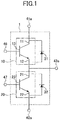
- FIG. 1 illustrates a circuit configuration of the semiconductor device according to the first embodiment.
- the semiconductor device 1 according to the first embodiment is an inverter circuit that has IGBTs 10 and 20, and diodes 31 and 32.
- the IGBT 10 includes a collector electrode 11, an emitter electrode 12, and a gate electrode 13.
- the IGBT 20 includes a collector electrode 21, an emitter electrode 22, and a gate electrode 23.
- the collector electrode 11 of the IGBT 10 is electrically connected with the cathode of the diode 31 and a high-potential-side power supply terminal 41a.
- the emitter electrode 12 of the IGBT 10 is electrically connected with the anode of the diode 31. In other words, the diode 31 is connected in reverse parallel with the IGBT 10.
- the gate electrode 13 of the IGBT 10 is electrically connected with at least one of control electrode terminals 46.
- the emitter electrode 22 of the IGBT 20 is electrically connected with the anode of the diode 32 and a low-potential-side power supply terminal 42a.
- the collector electrode 21 of the IGBT 20 is electrically connected with the cathode of the diode 32. In other words, the diode 32 is connected in reverse parallel with the IGBT 20.
- the gate electrode 13 of the IGBT 20 is electrically connected with at least one of control electrode terminals 47.
- the emitter electrode 12 of the IGBT 10 is electrically connected also with the collector electrode 21 of the IGBT 20, and also, is electrically connected with an output terminal 43a. Note that, because higher voltages are applied to the high-potential-side power supply terminal 41a, the low-potential-side power supply terminal 42a, and the output terminal 43a than those applied to the control electrode terminals 46 and 47, these three terminals may be referred to as high-voltage terminals.
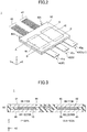
- FIG. 2 shows a perspective view illustrating the semiconductor device according to the first embodiment.
- FIG. 3 shows a sectional view of the semiconductor device according to the first embodiment taken along an A-A line of FIG. 2 .
- FIG. 4 shows a sectional view of the semiconductor device according to the first embodiment taken along a B-B line of FIG. 2 .
- FIG. 5 shows a perspective view illustrating an internal structure of the semiconductor device according to the first embodiment.
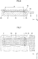
- FIG. 6 shows a sectional view of the semiconductor device according to the first embodiment taken along a C-C line of FIG. 5 .
- FIG. 7 shows a partial bottom view corresponding to FIG. 6 illustrating the semiconductor device according to the first embodiment.
- faces where metal plates 44 and 45 are exposed are referred to as top faces, and faces where metal plates 41 and 43 are exposed are referred to as bottom faces.
- faces from which the high-potential-side power supply terminal 41a, the low-potential-side power supply terminal 42a, and the output terminal 43a project are referred to as front faces.
- faces from which hanging lead terminal 41b, hanging lead terminal 43b, control electrode terminals 46, and the control electrode terminals 47 project are referred to as rear faces.
- the other faces are referred to as side faces.
- the metal plate 41 that includes the high-potential-side power supply terminal 41a and the hanging lead terminal 41b, the metal plate 42 that includes the low-potential-side power supply terminal 42a, and the metal plate 43 that includes the output terminal 43a and the hanging lead terminal 43b are installed in parallel at predetermined intervals in such a manner that the longitudinal directions thereof are approximately the same direction (Y-direction).
- control electrode terminals 46 are a plurality of metal lead terminals installed in parallel at predetermined intervals to have longitudinal directions that are approximately the same direction (the Y-direction) as the longitudinal direction of the metal plates 41.
- control electrode terminals 47 are a plurality of metal lead terminals installed in parallel at predetermined intervals to have longitudinal directions that are approximately the same direction (the Y-direction) as the longitudinal direction of the metal plates 43.
- Each of the materials of the metal plates 41, 42, and 43, and the control electrode terminals 46 and 47 may be, for example, copper (Cu), nickel (Ni), aluminum (Al), or the like.
- Each of the surfaces of the metal plates 41, 42, and 43, and the control electrode terminals 46 and 47 may be plated with silver (Ag), gold (Au), or the like.
- the IGBT 10 is mounted on the top face of the metal plate 41 in such a manner that the collector electrode 11 is electrically connected with the metal plate 41 through an electro-conductive bonding material such as tin-based solder (not shown).
- the collector electrode 11 is a p-type electrode
- the metal plate 41 connected with the collector electrode 11 may be referred to as a P-side.
- the diode 31 is mounted on the top face of the metal plate 41 in such a manner that the cathode is electrically connected with the metal plate 41 through an electro-conductive bonding material such as tin-based solder (not shown).
- the IGBT 10 and the diode 31 are arranged in the longitudinal direction (Y-direction) of the metal plate 41.
- the IGBT 20 is mounted on the top face of the metal plate 43 in such a manner that the collector electrode 21 is electrically connected with the metal plate 43 through an electro-conductive bonding material such as tin-based solder (not shown).
- the diode 32 is mounted on the top face of the metal plate 43 in such a manner that the cathode is electrically connected with the metal plate 43 through an electro-conductive bonding material such as tin-based solder (not shown).
- the IGBT 20 and the diode 32 are arranged in the longitudinal direction (Y-direction) of the metal plate 43.
- the thickness of the metal plate 41 where the IGBT 10 and the diode 31 are mounted (i.e., the thickness of the portion of the metal plate 41 other than the high-potential-side power supply terminal 41a and the hanging lead terminal 41b) may be, for example, around 2 through 3 millimeters.
- the thickness of the metal plate 43 where the IGBT 20 and the diode 32 are mounted (i.e., the thickness of the portion the metal plate 43 other than the output terminal 43a and the hanging lead terminal 43b) may be, for example, around 2 through 3 millimeters.
- the thickness of the metal plate 41 where the IGBT 10 and the diode 31 are mounted may be approximately the same as the thickness of the metal plate 43 where the IGBT 20 and the diode 32 are mounted.
- the thickness of the high-potential-side power supply terminal 41a and the hanging lead terminal 41b of the metal plate 41 may be less than the portion of the metal plate 41 where the IGBT 10 and the diode 31 are mounted, and, for example, may be on the order of 0. 5 mm.
- the thickness of the output terminal 43a and the hanging lead terminal 43b of the metal plate 43 may be less than the portion of the metal plate 43 where the IGBT 20 and the diode 32 are mounted, and, for example, may be on the order of 0. 5 mm.
- the metal plate 44 is placed in such a manner as to be electrically connected to the emitter electrode 12 of the IGBT 10 and the anode of the diode 31 via an electro-conductive spacer 61 (for example, a metal block made of a copper, or the like) and an electro-conductive bonding material such as tin-based solder.
- the electro-conductive spacer 61 (for example, a metal block made of a copper, or the like) is placed between the bottom face of the metal plate 44 and the top-face-side electrodes of the IGBT 10 and the diode 31.
- the metal plate 44 is electrically connected with the metal plate 43 via an electro-conductive bonding material (not shown) of tin-based solder or the like.
- the metal plate 45 is placed in such a manner as to be electrically connected to the emitter electrode 22 of the IGBT 20 and the anode of the diode 32 via an electro-conductive spacer 62 (for example, a metal block made of a copper, or the like) and an electro-conductive bonding material such as tin-based solder.
- an electro-conductive spacer 62 for example, a metal block made of a copper, or the like
- an electro-conductive bonding material such as tin-based solder.
- the electro-conductive spacer 62 (for example, a metal block made of a copper, or the like) is placed between the bottom face of the metal plate 45 and the top-face-side electrodes of the IGBT 20 and the diode 32.
- the metal plate 45 has a joint part 45j at a side face projecting toward the metal plate 44.
- the metal plate 42 has a joint part 42j at a side face projecting toward the control electrode terminals 46 and 47.
- the thickness of each of the joint parts 42j and 45j can be, for example, on the order of 0.5 mm.
- the bottom face of the joint part 45j of the metal plate 45 and the top face of the joint part 42j of the metal plate 42 face one another, and are electrically connected via an electro-conductive bonding material 81 (for example, tin-based solder, or the like).
- an electro-conductive bonding material 81 for example, tin-based solder, or the like.
- a ring-shaped groove 45x is formed to absorb a superfluous bonding material 81. Also on the top face of the joint part 42j, a groove 42x is formed to absorb a superfluous bonding material 81.
- the width of the groove 45x can be, for example, on the order of 400 through 600 ⁇ m.
- the depth of the groove 45x can be, for example, on the order of 200 through 300 ⁇ m.
- the sectional shape of the groove 45x is semicircular.
- the sectional shape of the groove 45x can be different from a semicircular shape.
- the sectional shape of the groove 45x may be semiellipse, rectangular, or the like.
- the groove 45x may have a shape different from a ring shape.
- the groove 45x is a typical example of a "groove" according to the present invention.
- An upper portion of the front end K of the joint part 42j (i.e., a portion near the joint part 45j of an end of the joint part 42j near the control electrode terminals 46 and 47) is fixed to a position overlapping with the groove 45x in plan view (in a state where the upper portion of the front end K of the joint part 42j falls into a position corresponding to the groove 45x) via the bonding material 81.
- M an area inside the groove 45x denotes an area where the joint part 45j and the joint part 42j are to be joined (i.e., where the bonding material 81 is to be placed) (hereinafter, referred to as a joint area M).
- the top face of the joint part 42j has a shape of a projection. Therefore, the upper portion of the front end K of the joint part 42j can be said to be the upper portion of the front end K of the projection. Also the upper portion of the rear end L of the projection (a portion near the joint part 45j of an end of the projection near the groove 42x) is fixed via the bonding material 81 to a position overlapping with the groove 45x in plan view.
- portions other than the upper portion of the front end K (the upper portion of the front end K of the joint part 42j) and the upper portion of the rear end L of the projection are fixed to positions overlapping with the groove 45x in plan view.
- the other portions than the upper portion of the front end K and the upper portion of the rear end L of the projection need not be fixed at positions overlapping with the groove 45x in plan view.
- the metal plates 43 and 44 have joint parts similar to those of the metal plates 42 and 45.
- the bottom face of the joint part of the metal plate 44 is electrically connected to the top face of the joint part of the metal plate 43 via an electro-conductive bonding material (for example, tin-based solder, of the like).
- an electro-conductive bonding material for example, tin-based solder, of the like.
- the thickness of the metal plate 44 can be, for example, on the order of 2 through 3 mm.
- the thickness of the metal plate 45 can be, for example, on the order of 2 through 3 mm.
- the metal plate 44 and the metal plate 45 may have approximately the same thicknesses.
- the materials of the metal plates 44 and 45 may be, for example, copper (Cu), nickel (Ni), aluminum (Al), or the like.
- the surfaces of the metal plates 44 and 45 may be plated with silver (Ag), gold (Au), or the like.
- the metal plate 45 is a typical example of a first plate-like part according to the present invention
- the joint part 45j is a typical example of a first joint part according to the present invention
- the metal plate 42 is a typical example of a second plate-like part according to the present invention
- the joint part 42j is a typical example of a second joint part according to the present invention.
- the respective metal lead terminals of the control electrode terminals 46 are electrically connected to the gate electrode 13 of the IGBT 10, a temperature sensor (not shown), and so forth, via bonding wires.
- the respective metal lead terminals of the control electrode terminals 47 are electrically connected to the gate electrode 23 of the IGBT 20, a temperature sensor (not shown), and so forth, via bonding wires.
- Each of the metal lead terminals of the control electrode terminals 46 and 47 can have a thickness of, for example, on the order of 0.5 mm.
- the bonding wires for example, metal wires such as gold wires or copper wires.
- the IGBTs 10 and 20, the diodes 31 and 32, the metal plates 41 through 45, the control electrode terminals 46 and 47, and the bonding wires are sealed with a sealing resin 50.
- the bottom faces of the metal plates 41 and 43 are at least partially exposed from the bottom face of the sealing resin 50.
- the top faces of the metal plates 44 and 45 are at least partially exposed from the top face of the sealing resin 50.
- each of the high-potential-side power supply terminal 41a of the metal plate 41, the low-potential-side power supply terminal 42a of the metal plate 42, and the output terminal 43a of the metal plate 43 at least partially projects from the front face of the sealing resin 50.
- each of the hanging lead terminal 41b formed on the end of the metal plate 41, the hanging lead terminal 43b formed on the end of the metal plate 43, the control electrode terminals 46, and the control electrode terminals 47 at least partially projects from the rear face of the sealing resin 50.
- a first direction (approximately, the X-direction) in which the IGBT 10 and the IGBT 20 are arranged is perpendicular to a second direction (approximately, the Y-direction) in which the hanging lead terminals 41b and 43b and the control electrode terminals 46 and 47 project.
- “perpendicular” in the present application is not “perpendicular” in its strict meaning, but means “approximately perpendicular”. For example, even if the angle between the first direction and the second direction is different from 90 degrees by ten and serval degrees due to a variation occurring in manufacturing, or the like, the angle is included in “perpendicular" angles.
- the sealing resin 50 can be made of, for example, an epoxy resin including a filler, or the like.
- the sealing resin 50 can have a thickness of, for example, on the order of 5 mm.
- the portions of the metal plates 41 through 45 exposed from the sealing resin 50 contribute discharging the heat generated by the IGBTs 10 and 20, and so forth.
- the metal plates 41 through 45 can be made from, for example, a lead frame. Note that if the metal plates 41 and 43 are made from a lead frame, the hanging lead terminals 41b and 43b are connected with a body (not shown) of the lead frame, and are portions cut off from the body of the lead frame after the body of the lead frame is sealed with the sealing resin 50.
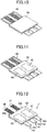
- FIGs. 8-12 illustrate manufacturing processes for the semiconductor device according to the first embodiment.
- a lead frame 40 that has a predetermined shape is prepared through press work, for example. Then, the IGBTs 10 and 20 and the diodes 31 and 32 (not shown in FIG. 8 , see FIGs. 3 and 4 ) are mounted on the lead frame 40 at predetermined positions via an electro-conductive bonding material such as tin-based solder (not shown).
- the electro-conductive spacer 61 (not shown in FIG. 8 , see FIGs. 3 and 4 ) is mounted, and, on the IGBT 20 and the diode 32, the electro-conductive spacer 62 (not shown in FIG. 8 , see FIGs. 3 and 4 ) is mounted.
- top face of the electro-conductive spacer 61, the top face of the electro-conductive spacer 62, the top face of the joint part 42j of a portion of the lead frame 40 to be the metal plate 42, and the top face of the joint part of a portion of the lead frame 40 to be the metal plate 43 are coated with an uncured electro-conductive bonding material 81 (for example, tin-based solder, or the like).
- an uncured electro-conductive bonding material 81 for example, tin-based solder, or the like.
- the metal plate 44 is mounted on the spacer 61 via the bonding material 81 (not shown). Also, on the spacer 62, the metal plate 45 is mounted via the bonding material 81 (not shown). Thereafter, a primer (such as a polyamide resin) is applied.
- a primer such as a polyamide resin
- the top face of the joint part 42j of the portion of the lead frame 40 to be the metal plate 42 is joined with the bottom face the joint part 45j of the metal plate 45 via the electro-conductive bonding material 81 (see FIGs. 6 and 7 ). Also, the top face of the joint part of the portion of the lead frame 40 to be the metal plate 43 is joined with the bottom face of the joint part of the metal plate 44 via the electro-conductive bonding material 81.
- the sealing resin 50 is formed.
- the top face of the sealing resin 50 cut off, and thus, the top faces of the metal plates 44 and 45 are exposed from the sealing resin 50.
- the lead frame 40 is cut at predetermined positions, and thus, the metal plates 41 through 43, the high-potential-side power supply terminal 41a, the low-potential-side power supply terminal 42a, the output terminal 43a, the hanging lead terminals 41b and 43b, and the control electrode terminals 46 and 47 are produced.
- the semiconductor device 1, illustrated in FIG. 2 and so forth is completed.
- an area N occurs where no portion of the bonding material 81 is present when, as illustrated in FIG. 13 , the joint part 42j is inclined and comes into contact with the joint part 45j. As a result, it is not possible to join the joint part 42j with the joint part 45j throughout the joint area M. Also, almost none of the bonding material 81 is present, and no filet is formed, near the upper portion of the front end K (in FIG. 13 , on the right side of the upper portion of the front end K).
- a groove 45x that is a bonding-material-thickness ensuring means for ensuring the thickness of the bonding material 81 between the upper portion of the front end K of the joint part 42j and the bottom face of the joint part 45j is formed.
- the upper portion of the front end K of the joint part 42j overlapping with the groove 45x in plan view, even if, as illustrated in FIG. 14 , the joint part 42j is inclined and comes into contact with the joint part 45j, the upper portion of the front end K is joined with the joint part 45j in the groove 45x. Thereby, it is possible to join the joint part 42j with the joint part 45j throughout the joint area M. Also near the upper portion of the front end K, the bonding material 81 can be ensured to have a predetermined thickness. Also, a fillet is formed between the upper portion of the front end K and the inner wall of the groove 45x.
- the bonding material 81 can be ensured to have a predetermined thickness also near the upper portion of the rear end L. Also, a fillet is formed between the upper portion of the rear end L and the inner wall of the groove 45x.
- a metal film that has wettability for the bonding material 81 better than that of the metal plate 42 may be formed on the bottom face of the joint part 45j including the inner wall of the groove 45x.
- the metal plate 42 is made of copper
- a gold film having the wettability for the bonding material 81 better than that of copper can be used as the metal film.
- the gold film can be formed using, for example, a plating method. It is also possible to install a nickel film, a palladium film, or the like, under the gold film.
- the bonding material 81 By thus forming the metal film that has wettability for the bonding material 81 better than that of the metal plate 42 on the bottom face of the joint part 45j including the inner wall of the groove 45x, the bonding material 81 more easily gathers into the groove 45x. Therefore, the bonding material 81 in the groove 45x is more likely to be ensured to have a predetermined thickness. As a result, the connection reliability between the joint part 42j and the joint part 45j can be further improved.
- FIG. 15 illustrates a state where one of joint parts is inclined in the semiconductor device according to a second variant of the first embodiment.
- a projection 45y is formed from the joint part 45j instead of the groove 45x.
- the projection 45y can be formed, for example, from the bottom face of the joint part 45j to have a ring shape.
- the upper portion of the front end K of the joint part 42j is fixed via the bonding material 81 nearer the outer edge of the bottom face of the joint part 45j than the area where the projection 45y is formed in plan view.
- the width of the projection 45y can be, for example, on the order of 400 through 600 ⁇ m.
- the height of the projection 45y can be, for example, on the order of 200 through 300 ⁇ m.
- the projection 45y that is a bonding-material-thickness ensuring means for ensuring the thickness of the bonding material 81 between the upper portion of the front end K of the joint part 42j and the bottom face of the joint part 45j is formed in a zone where the bottom face of the joint part 45j faces the top face of the joint part 42j.
- the upper portion of the front end K of the joint part 42j is placed nearer the outer edge of the bottom face of the joint part 45j than the area where the projection 45y is formed in plan view, the upper portion of the front end K is joined with the joint part 45j outside the projection 45y, even if, as shown in FIG. 15 , the joint part 42j is inclined and comes into contact with the joint part 45j. Thereby, the joint part 42j can be joined with the joint part 45j throughout the joint area M. Also, near the upper portion of the front end K, the bonding material 81 can be ensured to have a predetermined thickness. Also, a fillet is formed between the upper portion of the front end K and the bottom face of the joint part 45j.
- the bonding material 81 can be ensured to have a predetermined thickness also near the upper portion of the rear end L. Also, a fillet is formed between the upper portion of the rear end L and the bottom face of the joint part 45j.
- the following advantageous effects are acquired. That is, even if the joint part 42j is approximately parallel to the joint part 45j, a space greater than or equal to the height of the projection 45y is ensured between the joint part 42j and the joint part 45j, and is filled with the bonding material 81. As a result, it is possible to cause the thickness of the bonding material 81 to be at any time greater than or equal to an approximately certain value.
- FIG. 16 illustrates a state where one of joint parts is inclined in the semiconductor device according to a third variant of the first embodiment.
- FIG. 17 illustrates a state where the one of the joint parts is not inclined in the semiconductor device according to the third variant of the first embodiment.
- the bottom face of the joint part 45j is flat, and none of grooves and projections is formed there.
- the bonding material 81 contains many metal balls 85.
- the many metal balls 85 are dispersed.
- the metal balls 85 nickel balls each having, for example, a diameter on the order of 40 through 100 ⁇ m, or the like, can be used.
- the metal balls 85 need not be perfect spheres.
- the bonding material 81 containing many metal balls 85 even if, as shown in FIG. 16 , the joint part 42j is inclined, the joint part 42j does not come into contact with the joint part 45j, and a space on the order of the diameters of the metal balls 85 is ensured. The space is filled with the bonding material 81. Also, even if, as shown in FIG. 17 , the joint part 42j is approximately parallel to the joint part 45j, the joint part 42j does not come into contact with the joint part 45j, and a space on the order of the diameters of the metal balls 85 is ensured. The space is filled with the bonding material 81.
- the metal balls 85 ensure a space between the upper portion of the front end K of the joint part 42j and the bottom face of the joint part 45j, and the space is filled with the bonding material 81. Also, the metal balls 85 ensure a space between the upper portion of the rear end L of the joint part 42j and the bottom face of the joint part 45j, and the space is filled with the bonding material 81. Also, a fillet is formed between the upper portion of the front end K of the joint part 42j and the bottom face of the joint part 45, and between the upper portion of the rear end L of the joint part 42j and the bottom face of the joint part 45j.
- metal balls 85 that are present in a state of being dispersed in the bonding material 81
- bonding-material-thickness ensuring means for ensuring the thickness of the bonding material 81 between the upper portion of the front end K of the joint part 42j and the bottom face of the joint part 45j
- the following advantageous effects are acquired. That is, even if the joint part 42j is approximately parallel to the joint part 45j, it is possible to cause the thickness of the bonding material 81 to be at any time greater than or equal to an approximately certain value, because a space greater than or equal to the diameters of the metal balls 85 is ensured between the joint part 42j and the joint part 45j, and the space is filled with the bonding material 81. Also, wettability of the bonding material 81 is satisfactory around the metal balls 35. Thereby, it is possible to further improve connection reliability between the joint part 42j and the joint part 45j.
- the semiconductor device where the plurality of semiconductor elements (IGBTs and the diode) are arranged longitudinally and laterally has been illustrated.
- the present invention may be applied to, for example, a semiconductor device where two semiconductor elements into each of which an IGBT and a diode are integrated are arranged, or the like. Further, it is also possible to apply the present invention to, for example, a semiconductor device that has a single semiconductor element into which a IGBT and a diode are integrated.
Landscapes
- Cooling Or The Like Of Semiconductors Or Solid State Devices (AREA)
- Structures Or Materials For Encapsulating Or Coating Semiconductor Devices Or Solid State Devices (AREA)
- Wire Bonding (AREA)
Abstract
Description
- The present invention relates to a semiconductor device.
- Recently, a semiconductor device in which metal plates are electrically and thermally connected to top and bottom faces of a plurality of semiconductor elements, and the semiconductor elements are sealed with a resin, is known (for example, see Patent Reference No. 1). As one example of such a semiconductor device, a semiconductor device in which semiconductor elements such as insulated gate bipolar transistors (IGBTs), diodes, and so forth, are arranged longitudinally and laterally may be cited.
- An IGBT is such that the base of a bipolar transistor is replaced with the gate of a field effect transistor (FET), and has high speed performance and power durability of a bipolar transistor that is driven by a current, and also, power saving performance of a field effect transistor that is driven by a voltage. Therefore, such a semiconductor device can be used as a power semiconductor device that carries out switching operations.
- Patent Reference No. 1: Japanese Laid-Open Patent Application No.
2012-235081 - However, in such a semiconductor device, metal plates may be joined together with a bonding material (such as solder). In such a case, if one metal plate is inclined with respect to the other metal plate, connection reliability may be degraded because an end of the metal plate comes into contact with a surface of the other metal plate, and, near the contact position, a thickness of a bonding material cannot be ensured.
- The present invention has been devised in consideration of the above-mentioned point, and an object of the present invention is to provide a semiconductor device in which even if one of connected parts connected via a bonding material is inclined, connection reliability can be ensured.
- The present semiconductor device includes a semiconductor element; a first plate-like part that is made of an electric conductor, is electrically connected to an top-face-side electrode of the semiconductor element, and includes a first joint part that projects from a side face of the first plate-like part; and a second plate-like part that is made of an electric conductor, and includes a second joint part that projects from a side face of the second plate-like part. A bottom face of the first joint part and a top face of the second joint part face one another, and are electrically connected via an electro-conductive bonding material. A bonding-material-thickness ensuring means is provided in a zone where the bottom face of the first joint part and the top face of the second joint part face one another to ensure a thickness of the electro-conductive bonding material between an upper portion of a front end of the second joint part and the bottom face of the first joint part.
- According to the disclosed technology, it is possible to provide a semiconductor device in which, even if one of connected parts connected via a bonding material is inclined, connection reliability can be ensured.
-
-
FIG. 1 illustrates a circuit configuration of a semiconductor device according to a first embodiment; -
FIG. 2 shows a perspective view illustrating the semiconductor device according to the first embodiment; -
FIG. 3 shows a sectional view of the semiconductor device according to the first embodiment taken along an A-A line ofFIG. 2 ; -
FIG. 4 shows a sectional view of the semiconductor device according to the first embodiment taken along a B-B line ofFIG. 2 ; -
FIG. 5 shows a perspective view illustrating an internal configuration of the semiconductor device according to the first embodiment; -
FIG. 6 shows a sectional view of the semiconductor device according to the first embodiment taken along a C-C line ofFIG. 5 ; -
FIG. 7 shows a partial bottom view corresponding toFIG. 6 illustrating the semiconductor device according to the first embodiment; -
FIG. 8 illustrates a manufacturing process of the semiconductor device according to the first embodiment (No. 1) ; -
FIG. 9 illustrates a manufacturing process of the semiconductor device according to the first embodiment (No. 2); -
FIG. 10 illustrates a manufacturing process of the semiconductor device according to the first embodiment (No. 3); -
FIG. 11 illustrates a manufacturing process of the semiconductor device according to the first embodiment (No. 4); -
FIG. 12 illustrates a manufacturing process of the semiconductor device according to the first embodiment (No. 5); -
FIG. 13 illustrates a state where one of joint parts is inclined in a semiconductor device of a comparison example; -
FIG. 14 illustrates a state where one of joint parts is inclined in the semiconductor device according to the first embodiment; -
FIG. 15 illustrates a state where one of joint parts is inclined in a semiconductor device according to a second variant of the first embodiment; -
FIG. 16 illustrates a state where one of joint parts is inclined in a semiconductor device according to a third variant of the first embodiment; and -
FIG. 17 illustrates a state where the one of the joint parts is not inclined in the semiconductor device according to the third variant of the first embodiment. - Below, with reference to the drawings, modes for carrying out the invention will be described. For each embodiment, a semiconductor device in which four semiconductor elements (two IGBTs and two diodes) are arranged longitudinally and laterally will be described, as an example. However, an embodiment is not limited thereto. Note that, in each drawing, the same reference numerals are given to the same elements, and the duplicate description may be omitted.
- First, a circuit configuration of a semiconductor device according to a first embodiment will be described.
FIG. 1 illustrates a circuit configuration of the semiconductor device according to the first embodiment. With reference toFIG. 1 , thesemiconductor device 1 according to the first embodiment is an inverter circuit that hasIGBTs diodes - In the
semiconductor device 1, the IGBT 10 includes acollector electrode 11, anemitter electrode 12, and agate electrode 13. The IGBT 20 includes acollector electrode 21, anemitter electrode 22, and agate electrode 23. - The
collector electrode 11 of the IGBT 10 is electrically connected with the cathode of thediode 31 and a high-potential-sidepower supply terminal 41a. Theemitter electrode 12 of theIGBT 10 is electrically connected with the anode of thediode 31. In other words, thediode 31 is connected in reverse parallel with theIGBT 10. Thegate electrode 13 of the IGBT 10 is electrically connected with at least one ofcontrol electrode terminals 46. - The
emitter electrode 22 of theIGBT 20 is electrically connected with the anode of thediode 32 and a low-potential-sidepower supply terminal 42a. Thecollector electrode 21 of theIGBT 20 is electrically connected with the cathode of thediode 32. In other words, thediode 32 is connected in reverse parallel with theIGBT 20. Thegate electrode 13 of theIGBT 20 is electrically connected with at least one ofcontrol electrode terminals 47. - The
emitter electrode 12 of theIGBT 10 is electrically connected also with thecollector electrode 21 of theIGBT 20, and also, is electrically connected with anoutput terminal 43a. Note that, because higher voltages are applied to the high-potential-sidepower supply terminal 41a, the low-potential-sidepower supply terminal 42a, and theoutput terminal 43a than those applied to thecontrol electrode terminals - Next, a structure of the semiconductor device according to the first embodiment will be described.
FIG. 2 shows a perspective view illustrating the semiconductor device according to the first embodiment.FIG. 3 shows a sectional view of the semiconductor device according to the first embodiment taken along an A-A line ofFIG. 2 .FIG. 4 shows a sectional view of the semiconductor device according to the first embodiment taken along a B-B line ofFIG. 2 .FIG. 5 shows a perspective view illustrating an internal structure of the semiconductor device according to the first embodiment.FIG. 6 shows a sectional view of the semiconductor device according to the first embodiment taken along a C-C line ofFIG. 5 .FIG. 7 shows a partial bottom view corresponding toFIG. 6 illustrating the semiconductor device according to the first embodiment. - Note that, in the present application, concerning the
semiconductor device 1, faces wheremetal plates metal plates power supply terminal 41a, the low-potential-sidepower supply terminal 42a, and theoutput terminal 43a project are referred to as front faces. Also, faces from which hanginglead terminal 41b, hanginglead terminal 43b,control electrode terminals 46, and thecontrol electrode terminals 47 project are referred to as rear faces. Also, the other faces are referred to as side faces. - With reference to
FIGs. 2-7 , in thesemiconductor device 1, themetal plate 41 that includes the high-potential-sidepower supply terminal 41a and the hanginglead terminal 41b, themetal plate 42 that includes the low-potential-sidepower supply terminal 42a, and themetal plate 43 that includes theoutput terminal 43a and the hanginglead terminal 43b are installed in parallel at predetermined intervals in such a manner that the longitudinal directions thereof are approximately the same direction (Y-direction). - Also, the
control electrode terminals 46 are a plurality of metal lead terminals installed in parallel at predetermined intervals to have longitudinal directions that are approximately the same direction (the Y-direction) as the longitudinal direction of themetal plates 41. Also, thecontrol electrode terminals 47 are a plurality of metal lead terminals installed in parallel at predetermined intervals to have longitudinal directions that are approximately the same direction (the Y-direction) as the longitudinal direction of themetal plates 43. - Each of the materials of the
metal plates control electrode terminals metal plates control electrode terminals - The
IGBT 10 is mounted on the top face of themetal plate 41 in such a manner that thecollector electrode 11 is electrically connected with themetal plate 41 through an electro-conductive bonding material such as tin-based solder (not shown). Note that because thecollector electrode 11 is a p-type electrode, themetal plate 41 connected with thecollector electrode 11 may be referred to as a P-side. Also, thediode 31 is mounted on the top face of themetal plate 41 in such a manner that the cathode is electrically connected with themetal plate 41 through an electro-conductive bonding material such as tin-based solder (not shown). TheIGBT 10 and thediode 31 are arranged in the longitudinal direction (Y-direction) of themetal plate 41. - The
IGBT 20 is mounted on the top face of themetal plate 43 in such a manner that thecollector electrode 21 is electrically connected with themetal plate 43 through an electro-conductive bonding material such as tin-based solder (not shown). Also, thediode 32 is mounted on the top face of themetal plate 43 in such a manner that the cathode is electrically connected with themetal plate 43 through an electro-conductive bonding material such as tin-based solder (not shown). TheIGBT 20 and thediode 32 are arranged in the longitudinal direction (Y-direction) of themetal plate 43. - The thickness of the
metal plate 41 where theIGBT 10 and thediode 31 are mounted (i.e., the thickness of the portion of themetal plate 41 other than the high-potential-sidepower supply terminal 41a and the hanging lead terminal 41b) may be, for example, around 2 through 3 millimeters. The thickness of themetal plate 43 where theIGBT 20 and thediode 32 are mounted (i.e., the thickness of the portion themetal plate 43 other than theoutput terminal 43a and the hanging lead terminal 43b) may be, for example, around 2 through 3 millimeters. The thickness of themetal plate 41 where theIGBT 10 and thediode 31 are mounted may be approximately the same as the thickness of themetal plate 43 where theIGBT 20 and thediode 32 are mounted. - The thickness of the high-potential-side
power supply terminal 41a and the hanging lead terminal 41b of themetal plate 41 may be less than the portion of themetal plate 41 where theIGBT 10 and thediode 31 are mounted, and, for example, may be on the order of 0. 5 mm. The thickness of theoutput terminal 43a and the hanging lead terminal 43b of themetal plate 43 may be less than the portion of themetal plate 43 where theIGBT 20 and thediode 32 are mounted, and, for example, may be on the order of 0. 5 mm. - On the
IGBT 10 and thediode 31, themetal plate 44 is placed in such a manner as to be electrically connected to theemitter electrode 12 of theIGBT 10 and the anode of thediode 31 via an electro-conductive spacer 61 (for example, a metal block made of a copper, or the like) and an electro-conductive bonding material such as tin-based solder. In other words, the electro-conductive spacer 61 (for example, a metal block made of a copper, or the like) is placed between the bottom face of themetal plate 44 and the top-face-side electrodes of theIGBT 10 and thediode 31. Themetal plate 44 is electrically connected with themetal plate 43 via an electro-conductive bonding material (not shown) of tin-based solder or the like. - On the
IGBT 20 and thediode 32, themetal plate 45 is placed in such a manner as to be electrically connected to theemitter electrode 22 of theIGBT 20 and the anode of thediode 32 via an electro-conductive spacer 62 (for example, a metal block made of a copper, or the like) and an electro-conductive bonding material such as tin-based solder. In other words, the electro-conductive spacer 62 (for example, a metal block made of a copper, or the like) is placed between the bottom face of themetal plate 45 and the top-face-side electrodes of theIGBT 20 and thediode 32. - The
metal plate 45 has ajoint part 45j at a side face projecting toward themetal plate 44. Themetal plate 42 has ajoint part 42j at a side face projecting toward thecontrol electrode terminals joint parts - The bottom face of the
joint part 45j of themetal plate 45 and the top face of thejoint part 42j of themetal plate 42 face one another, and are electrically connected via an electro-conductive bonding material 81 (for example, tin-based solder, or the like). Note that, because theemitter electrode 22 is an n-type electrode, themetal plate 42 connected to theemitter electrode 22 may be referred to as an n-side. - At a peripheral portion on the bottom face of the
joint part 45j, a ring-shapedgroove 45x is formed to absorb asuperfluous bonding material 81. Also on the top face of thejoint part 42j, agroove 42x is formed to absorb asuperfluous bonding material 81. The width of thegroove 45x can be, for example, on the order of 400 through 600 µm. The depth of thegroove 45x can be, for example, on the order of 200 through 300 µm. - In
FIG. 6 and so forth, the sectional shape of thegroove 45x is semicircular. However, the sectional shape of thegroove 45x can be different from a semicircular shape. For example, the sectional shape of thegroove 45x may be semiellipse, rectangular, or the like. Further, as long as it is possible to ensure a sufficient volume to absorb asuperfluous bonding material 81, thegroove 45x may have a shape different from a ring shape. Note that, thegroove 45x is a typical example of a "groove" according to the present invention. - An upper portion of the front end K of the
joint part 42j (i.e., a portion near thejoint part 45j of an end of thejoint part 42j near thecontrol electrode terminals 46 and 47) is fixed to a position overlapping with thegroove 45x in plan view (in a state where the upper portion of the front end K of thejoint part 42j falls into a position corresponding to thegroove 45x) via thebonding material 81. Note that, M (an area inside thegroove 45x) denotes an area where thejoint part 45j and thejoint part 42j are to be joined (i.e., where thebonding material 81 is to be placed) (hereinafter, referred to as a joint area M). - As a result of the
groove 42x being formed, the top face of thejoint part 42j has a shape of a projection. Therefore, the upper portion of the front end K of thejoint part 42j can be said to be the upper portion of the front end K of the projection. Also the upper portion of the rear end L of the projection (a portion near thejoint part 45j of an end of the projection near thegroove 42x) is fixed via thebonding material 81 to a position overlapping with thegroove 45x in plan view. - In
FIG. 7 , also portions other than the upper portion of the front end K (the upper portion of the front end K of thejoint part 42j) and the upper portion of the rear end L of the projection are fixed to positions overlapping with thegroove 45x in plan view. However, the other portions than the upper portion of the front end K and the upper portion of the rear end L of the projection need not be fixed at positions overlapping with thegroove 45x in plan view. - Although corresponding enlarged views are omitted, also the
metal plates metal plates metal plate 44 is electrically connected to the top face of the joint part of themetal plate 43 via an electro-conductive bonding material (for example, tin-based solder, of the like). By forming the structures of the joint part of themetal plate 43 and the joint part of themetal plate 44 to be similar to those of thejoint part 42j and thejoint part 45j, similar advantageous effects (i.e., an improvement in connection reliability between thejoint part 42j and thejoint part 45j, as will be described later) can be acquired. However, themetal plates metal plates metal plate 42. - The thickness of the
metal plate 44 can be, for example, on the order of 2 through 3 mm. The thickness of themetal plate 45 can be, for example, on the order of 2 through 3 mm. Themetal plate 44 and themetal plate 45 may have approximately the same thicknesses. The materials of themetal plates metal plates - Note that the
metal plate 45 is a typical example of a first plate-like part according to the present invention, and thejoint part 45j is a typical example of a first joint part according to the present invention. Also, themetal plate 42 is a typical example of a second plate-like part according to the present invention, and thejoint part 42j is a typical example of a second joint part according to the present invention. - The respective metal lead terminals of the
control electrode terminals 46 are electrically connected to thegate electrode 13 of theIGBT 10, a temperature sensor (not shown), and so forth, via bonding wires. The respective metal lead terminals of thecontrol electrode terminals 47 are electrically connected to thegate electrode 23 of theIGBT 20, a temperature sensor (not shown), and so forth, via bonding wires. Each of the metal lead terminals of thecontrol electrode terminals - The
IGBTs diodes metal plates 41 through 45, thecontrol electrode terminals resin 50. However, the bottom faces of themetal plates resin 50. Also, the top faces of themetal plates resin 50. - Also, each of the high-potential-side
power supply terminal 41a of themetal plate 41, the low-potential-sidepower supply terminal 42a of themetal plate 42, and theoutput terminal 43a of themetal plate 43 at least partially projects from the front face of the sealingresin 50. Also, each of the hanginglead terminal 41b formed on the end of themetal plate 41, the hanginglead terminal 43b formed on the end of themetal plate 43, thecontrol electrode terminals 46, and thecontrol electrode terminals 47 at least partially projects from the rear face of the sealingresin 50. - A first direction (approximately, the X-direction) in which the
IGBT 10 and theIGBT 20 are arranged is perpendicular to a second direction (approximately, the Y-direction) in which the hanginglead terminals control electrode terminals - The sealing
resin 50 can be made of, for example, an epoxy resin including a filler, or the like. The sealingresin 50 can have a thickness of, for example, on the order of 5 mm. - The portions of the
metal plates 41 through 45 exposed from the sealingresin 50 contribute discharging the heat generated by theIGBTs metal plates 41 through 45 can be made from, for example, a lead frame. Note that if themetal plates lead terminals resin 50. - Next, a method of manufacturing the semiconductor device according to the first embodiment will be described.
FIGs. 8-12 illustrate manufacturing processes for the semiconductor device according to the first embodiment. - First, in a process illustrated in
FIG. 8 , alead frame 40 that has a predetermined shape is prepared through press work, for example. Then, theIGBTs diodes 31 and 32 (not shown inFIG. 8 , seeFIGs. 3 and4 ) are mounted on thelead frame 40 at predetermined positions via an electro-conductive bonding material such as tin-based solder (not shown). - Then, on the
IGBT 10 and thediode 31, the electro-conductive spacer 61 (not shown inFIG. 8 , seeFIGs. 3 and4 ) is mounted, and, on theIGBT 20 and thediode 32, the electro-conductive spacer 62 (not shown inFIG. 8 , seeFIGs. 3 and4 ) is mounted. Further, the top face of the electro-conductive spacer 61, the top face of the electro-conductive spacer 62, the top face of thejoint part 42j of a portion of thelead frame 40 to be themetal plate 42, and the top face of the joint part of a portion of thelead frame 40 to be themetal plate 43 are coated with an uncured electro-conductive bonding material 81 (for example, tin-based solder, or the like). - Next, in a process illustrated in
FIG. 9 , after wire bonding is carried out, themetal plate 44 is mounted on thespacer 61 via the bonding material 81 (not shown). Also, on thespacer 62, themetal plate 45 is mounted via the bonding material 81 (not shown). Thereafter, a primer (such as a polyamide resin) is applied. - In this process, the top face of the
joint part 42j of the portion of thelead frame 40 to be themetal plate 42 is joined with the bottom face thejoint part 45j of themetal plate 45 via the electro-conductive bonding material 81 (seeFIGs. 6 and 7 ). Also, the top face of the joint part of the portion of thelead frame 40 to be themetal plate 43 is joined with the bottom face of the joint part of themetal plate 44 via the electro-conductive bonding material 81. - Next, in a process illustrated in
FIG. 10 , molding is carried out, and the sealingresin 50 is formed. Next, in a process illustrated inFIG. 11 , the top face of the sealingresin 50 cut off, and thus, the top faces of themetal plates resin 50. Next, in a process illustrated inFIG. 12 , thelead frame 40 is cut at predetermined positions, and thus, themetal plates 41 through 43, the high-potential-sidepower supply terminal 41a, the low-potential-sidepower supply terminal 42a, theoutput terminal 43a, the hanginglead terminals control electrode terminals semiconductor device 1, illustrated inFIG. 2 and so forth, is completed. - In the process illustrated in
FIG. 9 , there may be a case where thejoint part 42j and thejoint part 45j are not parallel, as illustrated inFIG. 13 . This is because, as a result of the portion of thelead frame 40 to be themetal plate 42 has a cantilever structure (i.e., as a result of only one end being connected with the lead frame 40), a variation in the inclination of thejoint part 42j is large. - If the upper portion of the front end K of the
joint part 42j does not overlap with thegroove 45x in plan view, an area N occurs where no portion of thebonding material 81 is present when, as illustrated inFIG. 13 , thejoint part 42j is inclined and comes into contact with thejoint part 45j. As a result, it is not possible to join thejoint part 42j with thejoint part 45j throughout the joint area M. Also, almost none of thebonding material 81 is present, and no filet is formed, near the upper portion of the front end K (inFIG. 13 , on the right side of the upper portion of the front end K). - As a result, it is difficult to firmly join the
joint part 42j with thejoint part 45j, and it is not possible to ensure the durability of a joining part (thebonding material 81 that joins thejoint part 42j with thejoint part 45j). For example, if a crack occurs in thebonding material 81, the crack starts from an end of thebonding material 81. Therefore, if almost none of thebonding material 81 is present near the upper portion of the front end K (inFIG. 13 , on the right side of the upper portion of the front end K), a crack may be likely to occur there. - According to the present embodiment, in a zone where the bottom face of the
joint part 45j faces the top face of thejoint part 42j, agroove 45x that is a bonding-material-thickness ensuring means for ensuring the thickness of thebonding material 81 between the upper portion of the front end K of thejoint part 42j and the bottom face of thejoint part 45j is formed. - As a result of the upper portion of the front end K of the
joint part 42j overlapping with thegroove 45x in plan view, even if, as illustrated inFIG. 14 , thejoint part 42j is inclined and comes into contact with thejoint part 45j, the upper portion of the front end K is joined with thejoint part 45j in thegroove 45x. Thereby, it is possible to join thejoint part 42j with thejoint part 45j throughout the joint area M. Also near the upper portion of the front end K, thebonding material 81 can be ensured to have a predetermined thickness. Also, a fillet is formed between the upper portion of the front end K and the inner wall of thegroove 45x. - Also, because the upper portion of the rear end L of the
joint part 42j overlaps with thegroove 45x in plan view, thebonding material 81 can be ensured to have a predetermined thickness also near the upper portion of the rear end L. Also, a fillet is formed between the upper portion of the rear end L and the inner wall of thegroove 45x. - As a result of these states, it is possible to firmly join the
joint part 42j with thejoint part 45j. For example, if thesemiconductor device 1 is placed in a low-temperature environment and a high-temperature environment repetitiously, it is possible to reduce a likelihood of degradation (for example, an occurrence of a crack) in the joining part (thebonding material 81 that joins thejoint part 42j with thejoint part 45j). Thus, it is possible to improve the connection reliability between thejoint part 42j and thejoint part 45j. - Note that, in the structure according to the present embodiment, no problem occurs even if the
bonding material 81 overflows thegroove 45x. As can be seen fromFIG. 4 , thespacer 62 is present between themetal plate 45 and thediode 32, and the bonding material that joins thediode 32 to themetal plate 43 does not lie in the same plane as thebonding material 81. Therefore, even if thebonding material 81 overflows thegroove 45x, thediode 32 is not affected. Because themetal plates spacer 62, even if thebonding material 81 adheres thespacer 62, no problem occurs. - A metal film that has wettability for the
bonding material 81 better than that of themetal plate 42 may be formed on the bottom face of thejoint part 45j including the inner wall of thegroove 45x. For example, if themetal plate 42 is made of copper, a gold film having the wettability for thebonding material 81 better than that of copper can be used as the metal film. The gold film can be formed using, for example, a plating method. It is also possible to install a nickel film, a palladium film, or the like, under the gold film. - By thus forming the metal film that has wettability for the
bonding material 81 better than that of themetal plate 42 on the bottom face of thejoint part 45j including the inner wall of thegroove 45x, thebonding material 81 more easily gathers into thegroove 45x. Therefore, thebonding material 81 in thegroove 45x is more likely to be ensured to have a predetermined thickness. As a result, the connection reliability between thejoint part 42j and thejoint part 45j can be further improved. -
FIG. 15 illustrates a state where one of joint parts is inclined in the semiconductor device according to a second variant of the first embodiment. According to the semiconductor device in the second variant of the first embodiment, aprojection 45y is formed from thejoint part 45j instead of thegroove 45x. Theprojection 45y can be formed, for example, from the bottom face of thejoint part 45j to have a ring shape. - The upper portion of the front end K of the
joint part 42j is fixed via thebonding material 81 nearer the outer edge of the bottom face of thejoint part 45j than the area where theprojection 45y is formed in plan view. The width of theprojection 45y can be, for example, on the order of 400 through 600 µm. The height of theprojection 45y can be, for example, on the order of 200 through 300 µm. - Thus, according to the present embodiment, the
projection 45y that is a bonding-material-thickness ensuring means for ensuring the thickness of thebonding material 81 between the upper portion of the front end K of thejoint part 42j and the bottom face of thejoint part 45j is formed in a zone where the bottom face of thejoint part 45j faces the top face of thejoint part 42j. - Because the upper portion of the front end K of the
joint part 42j is placed nearer the outer edge of the bottom face of thejoint part 45j than the area where theprojection 45y is formed in plan view, the upper portion of the front end K is joined with thejoint part 45j outside theprojection 45y, even if, as shown inFIG. 15 , thejoint part 42j is inclined and comes into contact with thejoint part 45j. Thereby, thejoint part 42j can be joined with thejoint part 45j throughout the joint area M. Also, near the upper portion of the front end K, thebonding material 81 can be ensured to have a predetermined thickness. Also, a fillet is formed between the upper portion of the front end K and the bottom face of thejoint part 45j. - Also, because the upper portion of the rear end L of the
joint part 42j is placed nearer the outer edge of the bottom face of thejoint part 45j than an area where theprojection 45y is formed in plan view, thebonding material 81 can be ensured to have a predetermined thickness also near the upper portion of the rear end L. Also, a fillet is formed between the upper portion of the rear end L and the bottom face of thejoint part 45j. - Thereby, in addition to the advantageous effects of the first embodiment, the following advantageous effects are acquired. That is, even if the
joint part 42j is approximately parallel to thejoint part 45j, a space greater than or equal to the height of theprojection 45y is ensured between thejoint part 42j and thejoint part 45j, and is filled with thebonding material 81. As a result, it is possible to cause the thickness of thebonding material 81 to be at any time greater than or equal to an approximately certain value. - Also, in the same manner as the first variant of the first embodiment, it is more suitable to form a metal film that has wettability for the
bonding material 81 better than that of themetal plate 42 on the bottom face of thejoint part 45j including the outer walls of theprojection 45y. Note that, instead of forming theprojection 45y from the bottom face of thejoint part 45j of themetal plate 45, it is possible to acquire similar advantageous effects also by forming a projection from the top face of thejoint part 42j of themetal plate 42. -
FIG. 16 illustrates a state where one of joint parts is inclined in the semiconductor device according to a third variant of the first embodiment.FIG. 17 illustrates a state where the one of the joint parts is not inclined in the semiconductor device according to the third variant of the first embodiment. - In the semiconductor device according to the third variant of the first embodiment, the bottom face of the
joint part 45j is flat, and none of grooves and projections is formed there. Instead, thebonding material 81 containsmany metal balls 85. In other words, in thebonding material 81, themany metal balls 85 are dispersed. As themetal balls 85, nickel balls each having, for example, a diameter on the order of 40 through 100 µm, or the like, can be used. However, themetal balls 85 need not be perfect spheres. - As a result of the
bonding material 81 containingmany metal balls 85, even if, as shown inFIG. 16 , thejoint part 42j is inclined, thejoint part 42j does not come into contact with thejoint part 45j, and a space on the order of the diameters of themetal balls 85 is ensured. The space is filled with thebonding material 81. Also, even if, as shown inFIG. 17 , thejoint part 42j is approximately parallel to thejoint part 45j, thejoint part 42j does not come into contact with thejoint part 45j, and a space on the order of the diameters of themetal balls 85 is ensured. The space is filled with thebonding material 81. - That is, in any one of the cases of
FIGs. 16 and17 , themetal balls 85 ensure a space between the upper portion of the front end K of thejoint part 42j and the bottom face of thejoint part 45j, and the space is filled with thebonding material 81. Also, themetal balls 85 ensure a space between the upper portion of the rear end L of thejoint part 42j and the bottom face of thejoint part 45j, and the space is filled with thebonding material 81. Also, a fillet is formed between the upper portion of the front end K of thejoint part 42j and the bottom face of thejoint part 45, and between the upper portion of the rear end L of thejoint part 42j and the bottom face of thejoint part 45j. - Thus, according to the present embodiment, in a zone where the bottom face of the
joint part 45j faces the top face of thejoint part 42j, metal balls 85 (that are present in a state of being dispersed in the bonding material 81) that are a bonding-material-thickness ensuring means for ensuring the thickness of thebonding material 81 between the upper portion of the front end K of thejoint part 42j and the bottom face of thejoint part 45j are provided. - Thereby, in addition to the advantageous effects of the first embodiment, the following advantageous effects are acquired. That is, even if the
joint part 42j is approximately parallel to thejoint part 45j, it is possible to cause the thickness of thebonding material 81 to be at any time greater than or equal to an approximately certain value, because a space greater than or equal to the diameters of themetal balls 85 is ensured between thejoint part 42j and thejoint part 45j, and the space is filled with thebonding material 81. Also, wettability of thebonding material 81 is satisfactory around the metal balls 35. Thereby, it is possible to further improve connection reliability between thejoint part 42j and thejoint part 45j. - Also, in the same way as that of the first variant of the first embodiment, it is more suitable to form a metal film that has wettability for the
bonding material 81 better than themetal plate 42 on the bottom face of thejoint part 45j. - Thus, the preferred embodiment and the variants thereof have been described in detail. However, embodiments are not limited to the above-described embodiment and the variants thereof, and various changes and replacements can be made on the above-described embodiment and the variants thereof, without departing from the claimed scope.
- For example, for the above-mentioned embodiment, the semiconductor device where the plurality of semiconductor elements (IGBTs and the diode) are arranged longitudinally and laterally has been illustrated. However, the present invention may be applied to, for example, a semiconductor device where two semiconductor elements into each of which an IGBT and a diode are integrated are arranged, or the like. Further, it is also possible to apply the present invention to, for example, a semiconductor device that has a single semiconductor element into which a IGBT and a diode are integrated.
- Also, the above-described embodiment and variants thereof may be appropriately combined.
- The present international application is based on and claims the benefit of the priority of Japanese patent application No.
2014-046595, dated March 10, 2014 2014-046595 -
- 1
- a semiconductor device
- 10, 20
- IGBTs
- 11, 21
- collector electrodes
- 12, 22
- emitter electrodes
- 13, 23
- gate electrodes
- 31, 32
- diodes
- 40
- a lead frame
- 41a
- a high-potential-side power supply terminal
- 41b, 43b
- hanging lead terminals
- 41, 42, 43, 44, 45
- metal plates
- 42a
- a low-potential-side power supply terminal
- 42j, 45j
- joint parts
- 42x, 45x
- grooves
- 43a
- an output terminal
- 45y
- a projection
- 46, 47
- control electrode terminals
- 50
- a sealing resin
- 61, 62
- spacer
- 81
- a bonding material
- 85
- a metal ball
Claims (7)
- A semiconductor device comprising:a semiconductor element;a first plate-like part that is made of an electric conductor, is electrically connected to an top-face-side electrode of the semiconductor element, and includes a first joint part that projects from a side face of the first plate-like part; anda second plate-like part that is made of an electric conductor, and includes a second joint part that projects from a side face of the second plate-like part,whereina bottom face of the first joint part and a top face of the second joint part face one another, and are electrically connected via an electro-conductive bonding material, anda bonding-material-thickness ensuring means is provided in a zone where the bottom face of the first joint part and the top face of the second joint part face one another to ensure a thickness of the electro-conductive bonding material between an upper portion of a front end of the second joint part and the bottom face of the first joint part.
- The semiconductor device as claimed in claim 1, wherein
the bonding-material-thickness ensuring means is a groove formed from the bottom face of the first joint part, and
the upper portion of the front end of the second joint part is fixed via the bonding material at a position overlapping with the groove in plan view. - The semiconductor device as claimed in claim 1, wherein
the bonding-material-thickness ensuring means is a projection formed from the bottom face of the first joint part, and
the upper portion of the front end of the second joint part is fixed via the bonding material nearer an outer edge of the bottom face of the first joint part than the projection. - The semiconductor device as claimed in claim 1, wherein
the bonding-material-thickness ensuring means is a metal ball contained in the bonding material, and
the metal ball ensures a space between the upper portion of the front end of the second joint part and the bottom face of the first joint part, and the space is filled with the bonding material. - The semiconductor device as claimed in claim 2, wherein
the groove is formed to have a ring shape. - The semiconductor device as claimed in claim 5, wherein
a top face of the second joint part is a projection, and
an upper portion of a front end of the projection and an upper portion of a rear end of the projection are fixed via the bonding material at positions overlapping with the groove in plan view. - The semiconductor device as claimed in claim 1, wherein
a metal block is placed between a bottom face of the first plate-like part and the top-face-side electrode of the semiconductor element.
Applications Claiming Priority (2)
| Application Number | Priority Date | Filing Date | Title |
|---|---|---|---|
| JP2014046595A JP6294110B2 (en) | 2014-03-10 | 2014-03-10 | Semiconductor device |
| PCT/JP2015/050894 WO2015136968A1 (en) | 2014-03-10 | 2015-01-15 | Semiconductor device |
Publications (4)
| Publication Number | Publication Date |
|---|---|
| EP3118896A1 true EP3118896A1 (en) | 2017-01-18 |
| EP3118896A8 EP3118896A8 (en) | 2017-03-08 |
| EP3118896A4 EP3118896A4 (en) | 2017-03-15 |
| EP3118896B1 EP3118896B1 (en) | 2021-03-03 |
Family
ID=54071422
Family Applications (1)
| Application Number | Title | Priority Date | Filing Date |
|---|---|---|---|
| EP15760740.9A Active EP3118896B1 (en) | 2014-03-10 | 2015-01-15 | Semiconductor device |
Country Status (6)
| Country | Link |
|---|---|
| US (1) | US10103090B2 (en) |
| EP (1) | EP3118896B1 (en) |
| JP (1) | JP6294110B2 (en) |
| CN (1) | CN106062950B (en) |
| TW (1) | TW201539690A (en) |
| WO (1) | WO2015136968A1 (en) |
Cited By (1)
| Publication number | Priority date | Publication date | Assignee | Title |
|---|---|---|---|---|
| CN109755205A (en) * | 2017-11-08 | 2019-05-14 | 株式会社东芝 | semiconductor device |
Families Citing this family (15)
| Publication number | Priority date | Publication date | Assignee | Title |
|---|---|---|---|---|
| JP6221542B2 (en) * | 2013-09-16 | 2017-11-01 | 株式会社デンソー | Semiconductor device |
| JP6409733B2 (en) * | 2015-10-16 | 2018-10-24 | トヨタ自動車株式会社 | Semiconductor device |
| JP6772768B2 (en) * | 2016-11-09 | 2020-10-21 | 株式会社デンソー | Semiconductor device |
| JP6730450B2 (en) * | 2016-12-06 | 2020-07-29 | 株式会社東芝 | Semiconductor device |
| JP6512231B2 (en) | 2017-01-27 | 2019-05-15 | トヨタ自動車株式会社 | Semiconductor device |
| CN110214372B (en) * | 2017-02-20 | 2023-08-01 | 新电元工业株式会社 | Electronic device and connector |
| JP6586970B2 (en) | 2017-03-09 | 2019-10-09 | トヨタ自動車株式会社 | Semiconductor device |
| KR102048478B1 (en) * | 2018-03-20 | 2019-11-25 | 엘지전자 주식회사 | Power module of double-faced cooling and method for manufacturing thereof |
| JP6969501B2 (en) * | 2018-05-28 | 2021-11-24 | 株式会社デンソー | Semiconductor device |
| CN115609151B (en) * | 2018-08-30 | 2026-01-16 | 罗姆股份有限公司 | Semiconductor devices |
| US11482476B2 (en) | 2018-09-05 | 2022-10-25 | Hitachi Astemo, Ltd. | Power semiconductor device with an element installation conductor |
| JP7077893B2 (en) * | 2018-09-21 | 2022-05-31 | 株式会社デンソー | Semiconductor device |
| JP7107199B2 (en) * | 2018-12-07 | 2022-07-27 | 株式会社デンソー | semiconductor equipment |
| JP7120083B2 (en) | 2019-03-06 | 2022-08-17 | 株式会社デンソー | semiconductor equipment |
| JP7167907B2 (en) * | 2019-12-12 | 2022-11-09 | 株式会社デンソー | semiconductor equipment |
Family Cites Families (10)
| Publication number | Priority date | Publication date | Assignee | Title |
|---|---|---|---|---|
| JP4403665B2 (en) | 2001-03-14 | 2010-01-27 | 三菱電機株式会社 | Semiconductor device |
| JP2005136018A (en) | 2003-10-29 | 2005-05-26 | Denso Corp | Semiconductor device |
| JP4893303B2 (en) * | 2006-12-29 | 2012-03-07 | 株式会社デンソー | Semiconductor device |
| JP5947537B2 (en) | 2011-04-19 | 2016-07-06 | トヨタ自動車株式会社 | Semiconductor device and manufacturing method thereof |
| JP5488541B2 (en) * | 2011-07-04 | 2014-05-14 | 株式会社デンソー | Semiconductor device |
| JP5729314B2 (en) * | 2012-01-17 | 2015-06-03 | 株式会社デンソー | Semiconductor device and manufacturing method thereof |
| JP6155676B2 (en) * | 2013-02-11 | 2017-07-05 | 株式会社デンソー | Semiconductor device and manufacturing method thereof |
| JP6001473B2 (en) * | 2013-02-12 | 2016-10-05 | トヨタ自動車株式会社 | Manufacturing method of semiconductor device |
| JP5966979B2 (en) * | 2013-03-14 | 2016-08-10 | 株式会社デンソー | Semiconductor device and manufacturing method thereof |
| JP6065744B2 (en) * | 2013-05-20 | 2017-01-25 | 株式会社デンソー | Semiconductor module |
-
2014
- 2014-03-10 JP JP2014046595A patent/JP6294110B2/en active Active
-
2015
- 2015-01-15 CN CN201580012369.7A patent/CN106062950B/en active Active
- 2015-01-15 US US15/123,794 patent/US10103090B2/en active Active
- 2015-01-15 WO PCT/JP2015/050894 patent/WO2015136968A1/en not_active Ceased
- 2015-01-15 EP EP15760740.9A patent/EP3118896B1/en active Active
- 2015-01-28 TW TW104102902A patent/TW201539690A/en unknown
Cited By (5)
| Publication number | Priority date | Publication date | Assignee | Title |
|---|---|---|---|---|
| CN109755205A (en) * | 2017-11-08 | 2019-05-14 | 株式会社东芝 | semiconductor device |
| EP3483931A1 (en) * | 2017-11-08 | 2019-05-15 | Kabushiki Kaisha Toshiba | Semiconductor device |
| US11037863B2 (en) | 2017-11-08 | 2021-06-15 | Kabushiki Kaisha Toshiba | Semiconductor device |
| CN109755205B (en) * | 2017-11-08 | 2023-07-04 | 株式会社东芝 | Semiconductor device with a semiconductor device having a plurality of semiconductor chips |
| US11735505B2 (en) | 2017-11-08 | 2023-08-22 | Kabushiki Kaisha Toshiba | Semiconductor device |
Also Published As
| Publication number | Publication date |
|---|---|
| JP2015170810A (en) | 2015-09-28 |
| TW201539690A (en) | 2015-10-16 |
| JP6294110B2 (en) | 2018-03-14 |
| US10103090B2 (en) | 2018-10-16 |
| EP3118896B1 (en) | 2021-03-03 |
| CN106062950B (en) | 2019-05-28 |
| EP3118896A4 (en) | 2017-03-15 |
| TWI562310B (en) | 2016-12-11 |
| US20170018484A1 (en) | 2017-01-19 |
| EP3118896A8 (en) | 2017-03-08 |
| WO2015136968A1 (en) | 2015-09-17 |
| CN106062950A (en) | 2016-10-26 |
Similar Documents
| Publication | Publication Date | Title |
|---|---|---|
| US10103090B2 (en) | Semiconductor device | |
| US9224662B2 (en) | Semiconductor apparatus | |
| US9312211B2 (en) | Semiconductor device and manufacturing method thereof | |
| US9240371B2 (en) | Semiconductor module, semiconductor device having semiconductor module, and method of manufacturing semiconductor module | |
| US9418918B2 (en) | Lead for connection to a semiconductor device | |
| CN104641459B (en) | Semiconductor device | |
| US9076782B2 (en) | Semiconductor device and method of manufacturing same | |
| JP6898203B2 (en) | Power semiconductor module | |
| US20130249103A1 (en) | Semiconductor device | |
| US9502327B2 (en) | Semiconductor device and method for manufacturing the same | |
| JP2013004943A (en) | Semiconductor device and manufacturing method thereof | |
| CN108022900B (en) | Semiconductor device | |
| US9214418B2 (en) | Lead frame with radiator plate, method for manufacturing lead frame with radiator plate, semiconductor device, and method for manufacturing semiconductor device | |
| US20150262917A1 (en) | Semiconductor device and method of manufacturing the same | |
| JP6001473B2 (en) | Manufacturing method of semiconductor device | |
| US10283430B2 (en) | Power semiconductor device and method for manufacturing same | |
| US20210043598A1 (en) | Semiconductor device | |
| JP6001472B2 (en) | Manufacturing method of semiconductor device | |
| JP2018081980A (en) | Semiconductor device | |
| JP2012089563A (en) | Semiconductor module | |
| JP6316221B2 (en) | Semiconductor device | |
| JP2014187080A (en) | Semiconductor element, semiconductor device and composite module | |
| US20150380569A1 (en) | Diode having a plate-shaped semiconductor element | |
| JP2018032835A (en) | Manufacturing method of semiconductor device | |
| US20140264952A1 (en) | Supplementing wire bonds |
Legal Events
| Date | Code | Title | Description |
|---|---|---|---|
| PUAI | Public reference made under article 153(3) epc to a published international application that has entered the european phase |
Free format text: ORIGINAL CODE: 0009012 |
|
| STAA | Information on the status of an ep patent application or granted ep patent |
Free format text: STATUS: REQUEST FOR EXAMINATION WAS MADE |
|
| 17P | Request for examination filed |
Effective date: 20160808 |
|
| AK | Designated contracting states |
Kind code of ref document: A1 Designated state(s): AL AT BE BG CH CY CZ DE DK EE ES FI FR GB GR HR HU IE IS IT LI LT LU LV MC MK MT NL NO PL PT RO RS SE SI SK SM TR |
|
| AX | Request for extension of the european patent |
Extension state: BA ME |
|
| RAP1 | Party data changed (applicant data changed or rights of an application transferred) |
Owner name: DENSO CORPORATION Owner name: TOYOTA JIDOSHA KABUSHIKI KAISHA |
|
| RIN1 | Information on inventor provided before grant (corrected) |
Inventor name: KADOGUCHI, TAKUYA Inventor name: NISHIHATA, MASAYOSHI Inventor name: FUKUTANI, KEITA Inventor name: OKUMURA, TOMOMI Inventor name: KAWASHIMA, TAKANORI Inventor name: HIRANO, TAKAHIRO |
|
| A4 | Supplementary search report drawn up and despatched |
Effective date: 20170210 |
|
| RIC1 | Information provided on ipc code assigned before grant |
Ipc: H01L 25/07 20060101ALN20170206BHEP Ipc: H01L 23/495 20060101AFI20170206BHEP |
|
| DAX | Request for extension of the european patent (deleted) | ||
| STAA | Information on the status of an ep patent application or granted ep patent |
Free format text: STATUS: EXAMINATION IS IN PROGRESS |
|
| 17Q | First examination report despatched |
Effective date: 20190624 |
|
| REG | Reference to a national code |
Ref country code: DE Ref legal event code: R079 Ref document number: 602015066345 Country of ref document: DE Free format text: PREVIOUS MAIN CLASS: H01L0023480000 Ipc: H01L0023495000 |
|
| RIC1 | Information provided on ipc code assigned before grant |
Ipc: H01L 25/07 20060101ALN20200924BHEP Ipc: H01L 23/495 20060101AFI20200924BHEP |
|
| GRAP | Despatch of communication of intention to grant a patent |
Free format text: ORIGINAL CODE: EPIDOSNIGR1 |
|
| STAA | Information on the status of an ep patent application or granted ep patent |
Free format text: STATUS: GRANT OF PATENT IS INTENDED |
|
| RIC1 | Information provided on ipc code assigned before grant |
Ipc: H01L 23/495 20060101AFI20201012BHEP Ipc: H01L 25/07 20060101ALN20201012BHEP |
|
| INTG | Intention to grant announced |
Effective date: 20201116 |
|
| GRAS | Grant fee paid |
Free format text: ORIGINAL CODE: EPIDOSNIGR3 |
|
| GRAA | (expected) grant |
Free format text: ORIGINAL CODE: 0009210 |
|
| STAA | Information on the status of an ep patent application or granted ep patent |
Free format text: STATUS: THE PATENT HAS BEEN GRANTED |
|
| AK | Designated contracting states |
Kind code of ref document: B1 Designated state(s): AL AT BE BG CH CY CZ DE DK EE ES FI FR GB GR HR HU IE IS IT LI LT LU LV MC MK MT NL NO PL PT RO RS SE SI SK SM TR |
|
| RAP1 | Party data changed (applicant data changed or rights of an application transferred) |
Owner name: TOYOTA JIDOSHA KABUSHIKI KAISHA Owner name: DENSO CORPORATION |
|
| REG | Reference to a national code |
Ref country code: GB Ref legal event code: FG4D |
|
| RIN1 | Information on inventor provided before grant (corrected) |
Inventor name: NISHIHATA, MASAYOSHI Inventor name: OKUMURA, TOMOMI Inventor name: FUKUTANI, KEITA Inventor name: HIRANO, TAKAHIRO Inventor name: KAWASHIMA, TAKANORI Inventor name: KADOGUCHI, TAKUYA |
|
| REG | Reference to a national code |
Ref country code: AT Ref legal event code: REF Ref document number: 1368146 Country of ref document: AT Kind code of ref document: T Effective date: 20210315 Ref country code: CH Ref legal event code: EP |
|
| REG | Reference to a national code |
Ref country code: DE Ref legal event code: R096 Ref document number: 602015066345 Country of ref document: DE |
|
| REG | Reference to a national code |
Ref country code: IE Ref legal event code: FG4D |
|
| REG | Reference to a national code |
Ref country code: LT Ref legal event code: MG9D |
|
| PG25 | Lapsed in a contracting state [announced via postgrant information from national office to epo] |
Ref country code: LT Free format text: LAPSE BECAUSE OF FAILURE TO SUBMIT A TRANSLATION OF THE DESCRIPTION OR TO PAY THE FEE WITHIN THE PRESCRIBED TIME-LIMIT Effective date: 20210303 Ref country code: HR Free format text: LAPSE BECAUSE OF FAILURE TO SUBMIT A TRANSLATION OF THE DESCRIPTION OR TO PAY THE FEE WITHIN THE PRESCRIBED TIME-LIMIT Effective date: 20210303 Ref country code: FI Free format text: LAPSE BECAUSE OF FAILURE TO SUBMIT A TRANSLATION OF THE DESCRIPTION OR TO PAY THE FEE WITHIN THE PRESCRIBED TIME-LIMIT Effective date: 20210303 Ref country code: GR Free format text: LAPSE BECAUSE OF FAILURE TO SUBMIT A TRANSLATION OF THE DESCRIPTION OR TO PAY THE FEE WITHIN THE PRESCRIBED TIME-LIMIT Effective date: 20210604 Ref country code: BG Free format text: LAPSE BECAUSE OF FAILURE TO SUBMIT A TRANSLATION OF THE DESCRIPTION OR TO PAY THE FEE WITHIN THE PRESCRIBED TIME-LIMIT Effective date: 20210603 Ref country code: NO Free format text: LAPSE BECAUSE OF FAILURE TO SUBMIT A TRANSLATION OF THE DESCRIPTION OR TO PAY THE FEE WITHIN THE PRESCRIBED TIME-LIMIT Effective date: 20210603 |
|
| REG | Reference to a national code |
Ref country code: NL Ref legal event code: MP Effective date: 20210303 |
|
| REG | Reference to a national code |
Ref country code: AT Ref legal event code: MK05 Ref document number: 1368146 Country of ref document: AT Kind code of ref document: T Effective date: 20210303 |
|
| PG25 | Lapsed in a contracting state [announced via postgrant information from national office to epo] |
Ref country code: SE Free format text: LAPSE BECAUSE OF FAILURE TO SUBMIT A TRANSLATION OF THE DESCRIPTION OR TO PAY THE FEE WITHIN THE PRESCRIBED TIME-LIMIT Effective date: 20210303 Ref country code: RS Free format text: LAPSE BECAUSE OF FAILURE TO SUBMIT A TRANSLATION OF THE DESCRIPTION OR TO PAY THE FEE WITHIN THE PRESCRIBED TIME-LIMIT Effective date: 20210303 Ref country code: LV Free format text: LAPSE BECAUSE OF FAILURE TO SUBMIT A TRANSLATION OF THE DESCRIPTION OR TO PAY THE FEE WITHIN THE PRESCRIBED TIME-LIMIT Effective date: 20210303 Ref country code: PL Free format text: LAPSE BECAUSE OF FAILURE TO SUBMIT A TRANSLATION OF THE DESCRIPTION OR TO PAY THE FEE WITHIN THE PRESCRIBED TIME-LIMIT Effective date: 20210303 |
|
| PG25 | Lapsed in a contracting state [announced via postgrant information from national office to epo] |
Ref country code: NL Free format text: LAPSE BECAUSE OF FAILURE TO SUBMIT A TRANSLATION OF THE DESCRIPTION OR TO PAY THE FEE WITHIN THE PRESCRIBED TIME-LIMIT Effective date: 20210303 |
|
| PG25 | Lapsed in a contracting state [announced via postgrant information from national office to epo] |
Ref country code: SM Free format text: LAPSE BECAUSE OF FAILURE TO SUBMIT A TRANSLATION OF THE DESCRIPTION OR TO PAY THE FEE WITHIN THE PRESCRIBED TIME-LIMIT Effective date: 20210303 Ref country code: AT Free format text: LAPSE BECAUSE OF FAILURE TO SUBMIT A TRANSLATION OF THE DESCRIPTION OR TO PAY THE FEE WITHIN THE PRESCRIBED TIME-LIMIT Effective date: 20210303 Ref country code: CZ Free format text: LAPSE BECAUSE OF FAILURE TO SUBMIT A TRANSLATION OF THE DESCRIPTION OR TO PAY THE FEE WITHIN THE PRESCRIBED TIME-LIMIT Effective date: 20210303 Ref country code: EE Free format text: LAPSE BECAUSE OF FAILURE TO SUBMIT A TRANSLATION OF THE DESCRIPTION OR TO PAY THE FEE WITHIN THE PRESCRIBED TIME-LIMIT Effective date: 20210303 |
|
| PG25 | Lapsed in a contracting state [announced via postgrant information from national office to epo] |
Ref country code: SK Free format text: LAPSE BECAUSE OF FAILURE TO SUBMIT A TRANSLATION OF THE DESCRIPTION OR TO PAY THE FEE WITHIN THE PRESCRIBED TIME-LIMIT Effective date: 20210303 Ref country code: RO Free format text: LAPSE BECAUSE OF FAILURE TO SUBMIT A TRANSLATION OF THE DESCRIPTION OR TO PAY THE FEE WITHIN THE PRESCRIBED TIME-LIMIT Effective date: 20210303 Ref country code: PT Free format text: LAPSE BECAUSE OF FAILURE TO SUBMIT A TRANSLATION OF THE DESCRIPTION OR TO PAY THE FEE WITHIN THE PRESCRIBED TIME-LIMIT Effective date: 20210705 Ref country code: ES Free format text: LAPSE BECAUSE OF FAILURE TO SUBMIT A TRANSLATION OF THE DESCRIPTION OR TO PAY THE FEE WITHIN THE PRESCRIBED TIME-LIMIT Effective date: 20210303 Ref country code: IS Free format text: LAPSE BECAUSE OF FAILURE TO SUBMIT A TRANSLATION OF THE DESCRIPTION OR TO PAY THE FEE WITHIN THE PRESCRIBED TIME-LIMIT Effective date: 20210703 |
|
| REG | Reference to a national code |
Ref country code: DE Ref legal event code: R097 Ref document number: 602015066345 Country of ref document: DE |
|
| PLBE | No opposition filed within time limit |
Free format text: ORIGINAL CODE: 0009261 |
|
| STAA | Information on the status of an ep patent application or granted ep patent |
Free format text: STATUS: NO OPPOSITION FILED WITHIN TIME LIMIT |
|
| PG25 | Lapsed in a contracting state [announced via postgrant information from national office to epo] |
Ref country code: AL Free format text: LAPSE BECAUSE OF FAILURE TO SUBMIT A TRANSLATION OF THE DESCRIPTION OR TO PAY THE FEE WITHIN THE PRESCRIBED TIME-LIMIT Effective date: 20210303 Ref country code: DK Free format text: LAPSE BECAUSE OF FAILURE TO SUBMIT A TRANSLATION OF THE DESCRIPTION OR TO PAY THE FEE WITHIN THE PRESCRIBED TIME-LIMIT Effective date: 20210303 |
|
| 26N | No opposition filed |
Effective date: 20211206 |
|
| PG25 | Lapsed in a contracting state [announced via postgrant information from national office to epo] |
Ref country code: SI Free format text: LAPSE BECAUSE OF FAILURE TO SUBMIT A TRANSLATION OF THE DESCRIPTION OR TO PAY THE FEE WITHIN THE PRESCRIBED TIME-LIMIT Effective date: 20210303 |
|
| PG25 | Lapsed in a contracting state [announced via postgrant information from national office to epo] |
Ref country code: IT Free format text: LAPSE BECAUSE OF FAILURE TO SUBMIT A TRANSLATION OF THE DESCRIPTION OR TO PAY THE FEE WITHIN THE PRESCRIBED TIME-LIMIT Effective date: 20210303 |
|
| PG25 | Lapsed in a contracting state [announced via postgrant information from national office to epo] |
Ref country code: IS Free format text: LAPSE BECAUSE OF FAILURE TO SUBMIT A TRANSLATION OF THE DESCRIPTION OR TO PAY THE FEE WITHIN THE PRESCRIBED TIME-LIMIT Effective date: 20210703 |
|
| PG25 | Lapsed in a contracting state [announced via postgrant information from national office to epo] |
Ref country code: MC Free format text: LAPSE BECAUSE OF FAILURE TO SUBMIT A TRANSLATION OF THE DESCRIPTION OR TO PAY THE FEE WITHIN THE PRESCRIBED TIME-LIMIT Effective date: 20210303 |
|
| REG | Reference to a national code |
Ref country code: CH Ref legal event code: PL |
|
| GBPC | Gb: european patent ceased through non-payment of renewal fee |
Effective date: 20220115 |
|
| REG | Reference to a national code |
Ref country code: BE Ref legal event code: MM Effective date: 20220131 |
|
| PG25 | Lapsed in a contracting state [announced via postgrant information from national office to epo] |
Ref country code: LU Free format text: LAPSE BECAUSE OF NON-PAYMENT OF DUE FEES Effective date: 20220115 Ref country code: GB Free format text: LAPSE BECAUSE OF NON-PAYMENT OF DUE FEES Effective date: 20220115 |
|
| PG25 | Lapsed in a contracting state [announced via postgrant information from national office to epo] |
Ref country code: FR Free format text: LAPSE BECAUSE OF NON-PAYMENT OF DUE FEES Effective date: 20220131 Ref country code: BE Free format text: LAPSE BECAUSE OF NON-PAYMENT OF DUE FEES Effective date: 20220131 |
|
| PG25 | Lapsed in a contracting state [announced via postgrant information from national office to epo] |
Ref country code: LI Free format text: LAPSE BECAUSE OF NON-PAYMENT OF DUE FEES Effective date: 20220131 Ref country code: CH Free format text: LAPSE BECAUSE OF NON-PAYMENT OF DUE FEES Effective date: 20220131 |
|
| PG25 | Lapsed in a contracting state [announced via postgrant information from national office to epo] |
Ref country code: IE Free format text: LAPSE BECAUSE OF NON-PAYMENT OF DUE FEES Effective date: 20220115 |
|
| PG25 | Lapsed in a contracting state [announced via postgrant information from national office to epo] |
Ref country code: HU Free format text: LAPSE BECAUSE OF FAILURE TO SUBMIT A TRANSLATION OF THE DESCRIPTION OR TO PAY THE FEE WITHIN THE PRESCRIBED TIME-LIMIT; INVALID AB INITIO Effective date: 20150115 |
|
| PG25 | Lapsed in a contracting state [announced via postgrant information from national office to epo] |
Ref country code: MK Free format text: LAPSE BECAUSE OF FAILURE TO SUBMIT A TRANSLATION OF THE DESCRIPTION OR TO PAY THE FEE WITHIN THE PRESCRIBED TIME-LIMIT Effective date: 20210303 Ref country code: CY Free format text: LAPSE BECAUSE OF FAILURE TO SUBMIT A TRANSLATION OF THE DESCRIPTION OR TO PAY THE FEE WITHIN THE PRESCRIBED TIME-LIMIT Effective date: 20210303 |
|
| PG25 | Lapsed in a contracting state [announced via postgrant information from national office to epo] |
Ref country code: MT Free format text: LAPSE BECAUSE OF FAILURE TO SUBMIT A TRANSLATION OF THE DESCRIPTION OR TO PAY THE FEE WITHIN THE PRESCRIBED TIME-LIMIT Effective date: 20210303 |
|
| REG | Reference to a national code |
Ref country code: DE Ref legal event code: R079 Ref document number: 602015066345 Country of ref document: DE Free format text: PREVIOUS MAIN CLASS: H01L0023495000 Ipc: H10W0070400000 |
|
| PG25 | Lapsed in a contracting state [announced via postgrant information from national office to epo] |
Ref country code: TR Free format text: LAPSE BECAUSE OF FAILURE TO SUBMIT A TRANSLATION OF THE DESCRIPTION OR TO PAY THE FEE WITHIN THE PRESCRIBED TIME-LIMIT Effective date: 20210303 |
|
| PGFP | Annual fee paid to national office [announced via postgrant information from national office to epo] |
Ref country code: DE Payment date: 20260121 Year of fee payment: 12 |