EP3108607B1 - Control of tx/rx mode in serial half-duplex transceiver separately from communicating host - Google Patents
Control of tx/rx mode in serial half-duplex transceiver separately from communicating host Download PDFInfo
- Publication number
- EP3108607B1 EP3108607B1 EP15751545.3A EP15751545A EP3108607B1 EP 3108607 B1 EP3108607 B1 EP 3108607B1 EP 15751545 A EP15751545 A EP 15751545A EP 3108607 B1 EP3108607 B1 EP 3108607B1
- Authority
- EP
- European Patent Office
- Prior art keywords
- transceiver
- uart
- mode
- logic
- completion
- Prior art date
- Legal status (The legal status is an assumption and is not a legal conclusion. Google has not performed a legal analysis and makes no representation as to the accuracy of the status listed.)
- Active
Links
Images

Classifications
-
- G—PHYSICS
- G06—COMPUTING OR CALCULATING; COUNTING
- G06F—ELECTRIC DIGITAL DATA PROCESSING
- G06F13/00—Interconnection of, or transfer of information or other signals between, memories, input/output devices or central processing units
- G06F13/38—Information transfer, e.g. on bus
- G06F13/40—Bus structure
- G06F13/4063—Device-to-bus coupling
- G06F13/4068—Electrical coupling
- G06F13/4072—Drivers or receivers
-
- H—ELECTRICITY
- H04—ELECTRIC COMMUNICATION TECHNIQUE
- H04L—TRANSMISSION OF DIGITAL INFORMATION, e.g. TELEGRAPHIC COMMUNICATION
- H04L5/00—Arrangements affording multiple use of the transmission path
- H04L5/14—Two-way operation using the same type of signal, i.e. duplex
- H04L5/16—Half-duplex systems; Simplex/duplex switching; Transmission of break signals non-automatically inverting the direction of transmission
-
- G—PHYSICS
- G06—COMPUTING OR CALCULATING; COUNTING
- G06F—ELECTRIC DIGITAL DATA PROCESSING
- G06F13/00—Interconnection of, or transfer of information or other signals between, memories, input/output devices or central processing units
- G06F13/38—Information transfer, e.g. on bus
- G06F13/382—Information transfer, e.g. on bus using universal interface adapter
- G06F13/385—Information transfer, e.g. on bus using universal interface adapter for adaptation of a particular data processing system to different peripheral devices
-
- G—PHYSICS
- G06—COMPUTING OR CALCULATING; COUNTING
- G06F—ELECTRIC DIGITAL DATA PROCESSING
- G06F13/00—Interconnection of, or transfer of information or other signals between, memories, input/output devices or central processing units
- G06F13/38—Information transfer, e.g. on bus
- G06F13/42—Bus transfer protocol, e.g. handshake; Synchronisation
- G06F13/4282—Bus transfer protocol, e.g. handshake; Synchronisation on a serial bus, e.g. I2C bus, SPI bus
-
- H—ELECTRICITY
- H04—ELECTRIC COMMUNICATION TECHNIQUE
- H04B—TRANSMISSION
- H04B1/00—Details of transmission systems, not covered by a single one of groups H04B3/00 - H04B13/00; Details of transmission systems not characterised by the medium used for transmission
- H04B1/38—Transceivers, i.e. devices in which transmitter and receiver form a structural unit and in which at least one part is used for functions of transmitting and receiving
- H04B1/40—Circuits
- H04B1/401—Circuits for selecting or indicating operating mode
-
- H—ELECTRICITY
- H04—ELECTRIC COMMUNICATION TECHNIQUE
- H04B—TRANSMISSION
- H04B1/00—Details of transmission systems, not covered by a single one of groups H04B3/00 - H04B13/00; Details of transmission systems not characterised by the medium used for transmission
- H04B1/38—Transceivers, i.e. devices in which transmitter and receiver form a structural unit and in which at least one part is used for functions of transmitting and receiving
- H04B1/40—Circuits
- H04B1/44—Transmit/receive switching
- H04B1/48—Transmit/receive switching in circuits for connecting transmitter and receiver to a common transmission path, e.g. by energy of transmitter
-
- H—ELECTRICITY
- H04—ELECTRIC COMMUNICATION TECHNIQUE
- H04B—TRANSMISSION
- H04B1/00—Details of transmission systems, not covered by a single one of groups H04B3/00 - H04B13/00; Details of transmission systems not characterised by the medium used for transmission
- H04B1/38—Transceivers, i.e. devices in which transmitter and receiver form a structural unit and in which at least one part is used for functions of transmitting and receiving
- H04B1/40—Circuits
- H04B1/54—Circuits using the same frequency for two directions of communication
-
- G—PHYSICS
- G06—COMPUTING OR CALCULATING; COUNTING
- G06F—ELECTRIC DIGITAL DATA PROCESSING
- G06F2213/00—Indexing scheme relating to interconnection of, or transfer of information or other signals between, memories, input/output devices or central processing units
- G06F2213/0002—Serial port, e.g. RS232C
Definitions
- This relates generally to communication by an integrated circuit, and more particularly to control of serial half-duplex communication by an integrated circuit.
- Serial communication is common in industrial control applications. For example, serial half-duplex communication in accordance with RS-485 is widely used in automation systems. Applications such as factory automation systems often employ programmable logic controllers that use RS-485 for communication. Some systems are moving to Ethernet-based communication, but still require support for prevalent legacy systems. For example, RS-485 does not specify speed, format and protocol of the serial communication. Interoperability of devices from different manufacturers, even if similar, is not assured by merely complying with the signal level specifications.
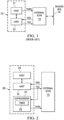
- FIG. 1 An example of a conventional communication system using serial half-duplex communication is shown diagrammatically in FIG. 1 , in which an integrated circuit 10 (e.g., a RISC microprocessor), including a host processor 11 and a universal asynchronous receiver/transmitter (UART) 12, cooperates with an external transceiver (XCVR) 13, such as a further integrated circuit.
- the UART 12 outputs to the transceiver 13 data TXD, which has been received from the host processor 11 and is transmitted by the transceiver onto a devices bus that has one or more connected devices, as shown diagrammatically at 14.
- the UART 12 receives from the transceiver 13 data RXD, which has been received by the transceiver 13 from the devices bus 14.
- the UART 12 provides this received data to the host processor 11.
- the host processor 11 provides to the transceiver 13 control signaling TX/RX, which appropriately enables and disables transmit operation and receive operation of the transceiver 13.
- a turn-around operation occurs when the host processor 11 (using the TX/RX signal) switches the transceiver 13 from a transmit (TX) mode to a receive (RX) mode, or vice versa.
- TX transmit
- RX receive
- turn-around time is the time required to transition the transceiver 13 from the TX mode (where transmit and receive operations of the transceiver 13 are respectively enabled and disabled) to the RX mode (where transmit and receive operations of the transceiver 13 are respectively disabled and enabled). This turn-around time begins when the last transmitted bit has completely traversed the transceiver 13.
- low latency e.g., aggressively low latency
- the turn-around from TX mode to RX mode should happen as soon as possible after the last transmitted bit has traversed the external transceiver (e.g., 13 in FIG. 1 ). Accordingly, the turn-around time from TX mode to RX mode should be as short as possible.
- US 2001/050905 relates to a device and method for switching transmission direction.
- WO 97/42730 relates to a half duplex UART control for single channel bi-directional wireless communications.
- An integrated circuit apparatus includes a host processor and a UART according to claim 1.
- the UART is coupled for communication with the host processor and configured for serial half-duplex communication with a transceiver that is external to the apparatus.
- the transceiver assumes a transmit mode of operation and a receive mode of operation during the serial half-duplex communication.
- the apparatus includes logic that is separate from the host processor, coupled to the UART, and responsive to operation of the UART for signaling to the transceiver respective indications of when to assume the transmit mode and when to assume the receive mode.
- the turn-around time associated with a transition from the TX mode to the RX mode of an external serial half-duplex transceiver could have a negative impact on the receive capability of the communication link. If the turn-around time is too long, some of the incoming RX data will be missed. Some link protocols require the turn-around operation to occur within two bit times. In at least one example, for communication at 115.2k baud, a turn-around time of two bit times would be well within the commonly requested 130us.
- the embodiments of the invention control TX/RX mode transitions of the external transceiver separately from the host processor, thereby avoiding slow turn-around times that may be associated with host processor control of the TX/RX mode transitions.
- Some embodiments provide, on the same integrated circuit as the host processor, logic that is separate from the host processor and controls the TX/RX mode transitions.
- FIG. 2 diagrammatically shows a communication system according to example embodiments.
- a serial half-duplex UART 12 within an integrated circuit 20 interfaces communications between a host processor 23 of the integrated circuit 20 and an external transceiver 13 (an integrated circuit in some embodiments) that is coupled in turn to a devices bus (not explicitly shown in FIG. 2 ).
- a coprocessor 21 in integrated circuits such as 10 and 20 of FIGS. 1 and 2 ) is used for controlling transitions between the TX and RX modes of the transceiver 13.
- the host processor 23 of FIG. 2 does not control the TX/RX mode transitions, whereas the host processor 11 of FIG. 1 does control those transitions.
- the coprocessor 21 controls the TX/RX mode transitions by exploiting knowledge of the timing and structure of serial data frames (also referred to as characters) transmitted at TXD by the UART 12. For example, frames transmitted at TXD usually begin with a start bit that is followed by a predetermined number of data bits (and one or more parity bits in some embodiments), which are in turn followed by one or more stop bits (usually one stop bit). In some embodiments, the frame contains eight data bits.
- the coprocessor 21 is coupled to the TXD output of the UART 12, and monitors the transmitted frame. Based on this monitoring of the transmitted frame, the coprocessor 21 outputs to the transceiver 13 signaling at TX/RX to indicate selection of the TX mode of the transceiver 13.
- the coprocessor 21 monitors the TXD output of the UART 12 to detect occurrence of a start bit. Detection of the start bit triggers the coprocessor 21 to signal (at TX/RX) immediately for the TX mode of the transceiver 13 (e.g., TX enabled and RX disabled). In some embodiments, the TX or RX mode is selected by simply toggling a single digital signal that, depending on its logic level, enables TX while disabling RX, or vice versa. Detection of the start bit also triggers operation of a timer function at 22 in coprocessor 21.
- the total amount of time required to transmit a frame which includes a start bit, multiple data (and optional parity) bits, and a stop bit, is known to the coprocessor 21.
- the timer function 22 When triggered by start bit detection, the timer function 22 begins timing the frame transmission. When the timer function 22 indicates that the frame transmission time has elapsed, the coprocessor 21 signals the transceiver 13 for selection of the RX mode.
- the timer function 22 implements a delay time immediately after the frame transmission time has elapsed.
- the coprocessor 21 waits until the delay time expires, and then signals for the RX mode.
- the delay time helps ensure that the stop bit has completely traversed the transceiver 13 before the switch to RX mode occurs.
- the coprocessor 21 continues to monitor the TXD output of the UART 12 during the delay time, thereby avoiding unnecessary toggling of the TX/RX select signal between frames in the event that a burst of consecutive frames is transmitted. Accordingly, the start bit of a second (or other subsequent) frame in a burst may be detected during the delay time, causing TX mode to remain selected.
- the delay has various time durations, such as at least one bit transmission time (bit time), some fraction of a bit time, and combinations of at least one bit time and some fraction of a bit time.
- firmware for the coprocessor 21 provides configuration parameters including one or more of the total transmission time for a frame, the bit time (usually the same for all bits of a frame), the frame structure, and the delay time.
- coprocessor 21 frees the host processor 23 from the task of switching the TX/RX mode of the transceiver 13. This is in contrast with conventional arrangements such as described above relative to FIG. 1 , wherein the host processor performs the task of switching the TX/RX mode.
- the mode control by coprocessor 21 helps to avoid occurrences of excessive turn-around times that may be associated with host processor control.
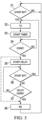
- FIG. 3 shows operations that may be performed according to example embodiments.
- the system of FIG. 2 is capable of performing the operations of FIG. 3 .
- monitoring for a start bit is shown. If a start bit is detected at 31, the TX mode is selected at 32, and a timer function begins at 33. When the timer expires at 34, a delay begins at 35. As shown at 36 and 37, monitoring for a start bit occurs at 36 during execution of the delay. If a start bit is detected at 36, operation proceeds to 32 where TX mode remains selected. If the delay time expires at 37 without detection of a start bit at 36, the RX mode is selected at 38, after which the next start bit is awaited at 31.
- FIG. 4 diagrammatically shows a communication system according to further example embodiments.
- the system of FIG. 4 is generally similar to that of FIG. 2 , except a coprocessor 41 within the integrated circuit 40 uses a line status register (LSR) 42 (conventionally available in the UART 12) to track progress of frame transmission on the TXD output of the UART 12.
- LSR line status register
- the LSR 42 conventionally indicates when transmit hold and shift registers of the UART 12 are empty, which is an indication that transmission of the frame is complete.
- FIG. 5 shows further operations that may be performed according to example embodiments.
- the system of FIG. 4 is capable of performing the operations of FIG. 5 .
- monitoring for a start bit is shown. If a start bit is detected at 51, the TX mode is selected at 52, and the LSR is monitored starting at 53. When the LSR indicates at 54 that transmission is complete, the RX mode is selected at 55, after which the next start bit is awaited at 51.
- the techniques described above relative to FIGS. 2-5 are easily scalable to accommodate multiple UARTs 12 in each of the integrated circuits 20 and 40, with multiple external transceivers 13 respectively coupled to the multiple UARTs.
- Such multiple UART/XCVR combinations are usually the case, such as in factory automation applications.
- the firmware for the coprocessor 21 or 41 provides configuration parameters to identify, for each of the multiple UART/XCVR combinations, which terminals of the integrated circuit are to be used by the coprocessor for monitoring the TXD output of the associated UART 12, and for outputting the TX/RX signal to the associated XCVR 13.
- the firmware for the coprocessor may be loaded in conventional fashion by the host processor (e.g., a Linux or RTOS host processor driver) written for the operating system used on the host processor.
- the transceivers 13 are provided as RS-485 transceivers, such as the commercially available SN65HVD82 RS-485 transceiver.
- the integrated circuits 20 and 40 are provided as RISC microprocessors, such as the commercially available AM335x/AM437x/AM57xx or similarly enabled microprocessors.
Landscapes
- Engineering & Computer Science (AREA)
- Theoretical Computer Science (AREA)
- Signal Processing (AREA)
- General Engineering & Computer Science (AREA)
- Computer Networks & Wireless Communication (AREA)
- Physics & Mathematics (AREA)
- General Physics & Mathematics (AREA)
- Computer Hardware Design (AREA)
- Communication Control (AREA)
- Transceivers (AREA)
- Bidirectional Digital Transmission (AREA)
Applications Claiming Priority (3)
| Application Number | Priority Date | Filing Date | Title |
|---|---|---|---|
| US201461941922P | 2014-02-19 | 2014-02-19 | |
| US14/311,355 US9246534B2 (en) | 2014-02-19 | 2014-06-23 | Controling Tx/Rx mode in serial half-duplex UART separately from host |
| PCT/US2015/016512 WO2015127014A1 (en) | 2014-02-19 | 2015-02-19 | Control of tx/rx mode in serial half-duplex transceiver separately from communicating host |
Publications (3)
| Publication Number | Publication Date |
|---|---|
| EP3108607A1 EP3108607A1 (en) | 2016-12-28 |
| EP3108607A4 EP3108607A4 (en) | 2017-08-23 |
| EP3108607B1 true EP3108607B1 (en) | 2024-04-10 |
Family
ID=53878937
Family Applications (1)
| Application Number | Title | Priority Date | Filing Date |
|---|---|---|---|
| EP15751545.3A Active EP3108607B1 (en) | 2014-02-19 | 2015-02-19 | Control of tx/rx mode in serial half-duplex transceiver separately from communicating host |
Country Status (5)
| Country | Link |
|---|---|
| US (2) | US9246534B2 (https=) |
| EP (1) | EP3108607B1 (https=) |
| JP (1) | JP6496747B2 (https=) |
| CN (1) | CN106031077B (https=) |
| WO (1) | WO2015127014A1 (https=) |
Families Citing this family (3)
| Publication number | Priority date | Publication date | Assignee | Title |
|---|---|---|---|---|
| DE102020200804A1 (de) * | 2020-01-23 | 2021-07-29 | Robert Bosch Gesellschaft mit beschränkter Haftung | Sende-/Empfangseinrichtung und Kommunikationssteuereinrichtung für eine Teilnehmerstation eines seriellen Bussystems und Verfahren zur Kommunikation in einem seriellen Bussystem |
| CN112053544B (zh) * | 2020-09-16 | 2022-02-25 | 深圳市爱尚智联科技有限公司 | 单线双向半双工蓝牙ble遥控模块及遥控方法 |
| CN115412392B (zh) * | 2021-05-28 | 2024-05-10 | 精拓科技股份有限公司 | Rs-485电路与通信系统 |
Family Cites Families (20)
| Publication number | Priority date | Publication date | Assignee | Title |
|---|---|---|---|---|
| CA1226960A (en) * | 1985-06-28 | 1987-09-15 | Gregory F. Hicks | Rate adaptation circuit and method for asynchronous data on digital networks |
| US4740957A (en) * | 1985-07-26 | 1988-04-26 | American Telephone And Telegraph Company | Asynchronous addressable electronic key telephone system |
| US5199105A (en) * | 1988-09-14 | 1993-03-30 | National Semiconductor Corporation | Universal asynchronous receiver/transmitter |
| DE69027531D1 (de) * | 1990-09-28 | 1996-07-25 | Ibm | Datenübertragungseinheit (DCE) mit einer durch ein Verarbeitungsmittel gesteuerten Taktgeberanordnung |
| US5742502A (en) * | 1995-04-25 | 1998-04-21 | Motorola, Inc. | Method and apparatus for generating synchronous data transmissions in a device having a universal asynchronous receiver/transmitter |
| US5918024A (en) | 1996-05-08 | 1999-06-29 | Ericsson, Inc. | Method and apparatus for providing single channel communications |
| US5953372A (en) | 1996-12-13 | 1999-09-14 | Standard Microsystems Corporation | Loopback transmission testing in a communications device |
| US5964853A (en) * | 1997-03-07 | 1999-10-12 | National Semiconductor Corp. | Interface controller including hardware mechanism to handle PS/2 interface |
| US5959979A (en) * | 1997-05-05 | 1999-09-28 | Northrop Grumman Corporation | Half-duplex communication system for telemetry modems |
| ES2148892T3 (es) * | 1997-11-13 | 2000-10-16 | Optimay Gmbh | Deteccion de velocidad de baudios en una transmision en serie de datos. |
| US6272452B1 (en) * | 1998-04-02 | 2001-08-07 | Ati Technologies, Inc. | Universal asynchronous receiver transmitter (UART) emulation stage for modem communication |
| US6385210B1 (en) | 1998-04-17 | 2002-05-07 | Ford Global Technologies, Inc. | Method for detecting and resolving data corruption in a UART based communication network |
| KR100268885B1 (ko) * | 1998-09-10 | 2000-10-16 | 김영환 | 비동기 데이터 송수신 장치 |
| CN1188953C (zh) * | 1998-09-28 | 2005-02-09 | 索尼电脑娱乐公司 | 红外收发机和信号收发方法 |
| US6529970B1 (en) * | 2000-04-13 | 2003-03-04 | Fujitsu Microelectronics America, Inc. | Method and microprocessor with fast program downloading features |
| TW513882B (en) * | 2000-06-13 | 2002-12-11 | Moxa Technologies Co Ltd | Switching device and switching method for transmission direction |
| US7372914B2 (en) * | 2000-11-16 | 2008-05-13 | Invensys Systems, Inc. | Control system methods and apparatus for inductive communication across an isolation barrier |
| CN1160896C (zh) * | 2001-06-04 | 2004-08-04 | 四零四科技股份有限公司 | 传输方向切换装置与切换方法 |
| WO2003088568A2 (en) * | 2002-04-12 | 2003-10-23 | Thomson Licensing S.A. | Digital control circuit for serial uart transmissions |
| US8121128B2 (en) | 2008-02-26 | 2012-02-21 | Qualcomm Incorporated | Method and apparatus for link control in a wireless communication system |
-
2014
- 2014-06-23 US US14/311,355 patent/US9246534B2/en active Active
-
2015
- 2015-02-19 WO PCT/US2015/016512 patent/WO2015127014A1/en not_active Ceased
- 2015-02-19 CN CN201580009442.5A patent/CN106031077B/zh active Active
- 2015-02-19 EP EP15751545.3A patent/EP3108607B1/en active Active
- 2015-02-19 JP JP2016553297A patent/JP6496747B2/ja active Active
- 2015-12-14 US US14/967,959 patent/US9892080B2/en active Active
Also Published As
| Publication number | Publication date |
|---|---|
| US20150270863A1 (en) | 2015-09-24 |
| US9246534B2 (en) | 2016-01-26 |
| JP2017513283A (ja) | 2017-05-25 |
| EP3108607A1 (en) | 2016-12-28 |
| WO2015127014A1 (en) | 2015-08-27 |
| CN106031077A (zh) | 2016-10-12 |
| US9892080B2 (en) | 2018-02-13 |
| US20160098373A1 (en) | 2016-04-07 |
| JP6496747B2 (ja) | 2019-04-03 |
| EP3108607A4 (en) | 2017-08-23 |
| CN106031077B (zh) | 2019-11-12 |
Similar Documents
| Publication | Publication Date | Title |
|---|---|---|
| EP2867780B1 (en) | Device disconnect detection | |
| EP2961098B1 (en) | Method, device and system for processing pcie link failure | |
| EP3269095B1 (en) | High speed isolated and optical usb | |
| EP2530601B1 (en) | Redriver circuits with power saving modes | |
| US9767064B2 (en) | Low power universal serial bus | |
| EP3696684B1 (en) | Fast link turnaround using mipi d-phy | |
| EP3108607B1 (en) | Control of tx/rx mode in serial half-duplex transceiver separately from communicating host | |
| US9825754B2 (en) | Independent UART BRK detection | |
| CN104142901A (zh) | 一种具有传输优先级的串口复用器实现方法 | |
| EP2867781B1 (en) | Explicit control message signaling | |
| US12056074B2 (en) | Processing system, related integrated circuit, system and method | |
| JP6014627B2 (ja) | 電子機器の電力モード切り替えシステム | |
| JP4643499B2 (ja) | 情報処理装置 | |
| KR101449274B1 (ko) | 유효 채널을 이용하는 와치독 및 그 동작방법 | |
| CN110608502A (zh) | 基于单线半双工通信的空调通信方法和空调器 | |
| CN113127401B (zh) | 一种耳机盒与耳机的通信方法和系统 | |
| KR100275705B1 (ko) | 데이터 송/수신 시스템 | |
| KR101041855B1 (ko) | 망 상태 전문 전송제어장치 및 방법 | |
| US7610420B2 (en) | Data aggregation-distribution apparatus, date transmission system and method thereof | |
| JPH11177654A (ja) | データ送受信方法 | |
| KR20110069534A (ko) | 2개의 신호를 이용한 통신 인터페이스 장치 |
Legal Events
| Date | Code | Title | Description |
|---|---|---|---|
| PUAI | Public reference made under article 153(3) epc to a published international application that has entered the european phase |
Free format text: ORIGINAL CODE: 0009012 |
|
| STAA | Information on the status of an ep patent application or granted ep patent |
Free format text: STATUS: REQUEST FOR EXAMINATION WAS MADE |
|
| 17P | Request for examination filed |
Effective date: 20160919 |
|
| AK | Designated contracting states |
Kind code of ref document: A1 Designated state(s): AL AT BE BG CH CY CZ DE DK EE ES FI FR GB GR HR HU IE IS IT LI LT LU LV MC MK MT NL NO PL PT RO RS SE SI SK SM TR |
|
| AX | Request for extension of the european patent |
Extension state: BA ME |
|
| RIN1 | Information on inventor provided before grant (corrected) |
Inventor name: PATTON, SCHUYLER T. JR. Inventor name: PRAKASH, PUNYA Inventor name: WATKINS, MELISSA MARIE Inventor name: GRIFFIS, BRADLEY JAMES Inventor name: MOHAMMAD, SAQIB NADEEM |
|
| DAX | Request for extension of the european patent (deleted) | ||
| A4 | Supplementary search report drawn up and despatched |
Effective date: 20170721 |
|
| RIC1 | Information provided on ipc code assigned before grant |
Ipc: G06F 13/42 20060101ALI20170717BHEP Ipc: G06F 13/38 20060101AFI20170717BHEP |
|
| STAA | Information on the status of an ep patent application or granted ep patent |
Free format text: STATUS: EXAMINATION IS IN PROGRESS |
|
| 17Q | First examination report despatched |
Effective date: 20180403 |
|
| APBK | Appeal reference recorded |
Free format text: ORIGINAL CODE: EPIDOSNREFNE |
|
| APBN | Date of receipt of notice of appeal recorded |
Free format text: ORIGINAL CODE: EPIDOSNNOA2E |
|
| APBR | Date of receipt of statement of grounds of appeal recorded |
Free format text: ORIGINAL CODE: EPIDOSNNOA3E |
|
| APAF | Appeal reference modified |
Free format text: ORIGINAL CODE: EPIDOSCREFNE |
|
| APBT | Appeal procedure closed |
Free format text: ORIGINAL CODE: EPIDOSNNOA9E |
|
| GRAP | Despatch of communication of intention to grant a patent |
Free format text: ORIGINAL CODE: EPIDOSNIGR1 |
|
| STAA | Information on the status of an ep patent application or granted ep patent |
Free format text: STATUS: GRANT OF PATENT IS INTENDED |
|
| INTG | Intention to grant announced |
Effective date: 20231113 |
|
| GRAS | Grant fee paid |
Free format text: ORIGINAL CODE: EPIDOSNIGR3 |
|
| GRAA | (expected) grant |
Free format text: ORIGINAL CODE: 0009210 |
|
| STAA | Information on the status of an ep patent application or granted ep patent |
Free format text: STATUS: THE PATENT HAS BEEN GRANTED |
|
| P01 | Opt-out of the competence of the unified patent court (upc) registered |
Effective date: 20240212 |
|
| AK | Designated contracting states |
Kind code of ref document: B1 Designated state(s): AL AT BE BG CH CY CZ DE DK EE ES FI FR GB GR HR HU IE IS IT LI LT LU LV MC MK MT NL NO PL PT RO RS SE SI SK SM TR |
|
| REG | Reference to a national code |
Ref country code: GB Ref legal event code: FG4D |
|
| REG | Reference to a national code |
Ref country code: CH Ref legal event code: EP |
|
| REG | Reference to a national code |
Ref country code: DE Ref legal event code: R096 Ref document number: 602015088253 Country of ref document: DE |
|
| REG | Reference to a national code |
Ref country code: IE Ref legal event code: FG4D |
|
| REG | Reference to a national code |
Ref country code: LT Ref legal event code: MG9D |
|
| REG | Reference to a national code |
Ref country code: NL Ref legal event code: MP Effective date: 20240410 |
|
| REG | Reference to a national code |
Ref country code: AT Ref legal event code: MK05 Ref document number: 1675613 Country of ref document: AT Kind code of ref document: T Effective date: 20240410 |
|
| PG25 | Lapsed in a contracting state [announced via postgrant information from national office to epo] |
Ref country code: NL Free format text: LAPSE BECAUSE OF FAILURE TO SUBMIT A TRANSLATION OF THE DESCRIPTION OR TO PAY THE FEE WITHIN THE PRESCRIBED TIME-LIMIT Effective date: 20240410 |
|
| PG25 | Lapsed in a contracting state [announced via postgrant information from national office to epo] |
Ref country code: NL Free format text: LAPSE BECAUSE OF FAILURE TO SUBMIT A TRANSLATION OF THE DESCRIPTION OR TO PAY THE FEE WITHIN THE PRESCRIBED TIME-LIMIT Effective date: 20240410 |
|
| PG25 | Lapsed in a contracting state [announced via postgrant information from national office to epo] |
Ref country code: IS Free format text: LAPSE BECAUSE OF FAILURE TO SUBMIT A TRANSLATION OF THE DESCRIPTION OR TO PAY THE FEE WITHIN THE PRESCRIBED TIME-LIMIT Effective date: 20240810 |
|
| PG25 | Lapsed in a contracting state [announced via postgrant information from national office to epo] |
Ref country code: BG Free format text: LAPSE BECAUSE OF FAILURE TO SUBMIT A TRANSLATION OF THE DESCRIPTION OR TO PAY THE FEE WITHIN THE PRESCRIBED TIME-LIMIT Effective date: 20240410 |
|
| PG25 | Lapsed in a contracting state [announced via postgrant information from national office to epo] |
Ref country code: FI Free format text: LAPSE BECAUSE OF FAILURE TO SUBMIT A TRANSLATION OF THE DESCRIPTION OR TO PAY THE FEE WITHIN THE PRESCRIBED TIME-LIMIT Effective date: 20240410 Ref country code: HR Free format text: LAPSE BECAUSE OF FAILURE TO SUBMIT A TRANSLATION OF THE DESCRIPTION OR TO PAY THE FEE WITHIN THE PRESCRIBED TIME-LIMIT Effective date: 20240410 |
|
| PG25 | Lapsed in a contracting state [announced via postgrant information from national office to epo] |
Ref country code: GR Free format text: LAPSE BECAUSE OF FAILURE TO SUBMIT A TRANSLATION OF THE DESCRIPTION OR TO PAY THE FEE WITHIN THE PRESCRIBED TIME-LIMIT Effective date: 20240711 |
|
| PG25 | Lapsed in a contracting state [announced via postgrant information from national office to epo] |
Ref country code: PT Free format text: LAPSE BECAUSE OF FAILURE TO SUBMIT A TRANSLATION OF THE DESCRIPTION OR TO PAY THE FEE WITHIN THE PRESCRIBED TIME-LIMIT Effective date: 20240812 |
|
| PG25 | Lapsed in a contracting state [announced via postgrant information from national office to epo] |
Ref country code: ES Free format text: LAPSE BECAUSE OF FAILURE TO SUBMIT A TRANSLATION OF THE DESCRIPTION OR TO PAY THE FEE WITHIN THE PRESCRIBED TIME-LIMIT Effective date: 20240410 |
|
| PG25 | Lapsed in a contracting state [announced via postgrant information from national office to epo] |
Ref country code: AT Free format text: LAPSE BECAUSE OF FAILURE TO SUBMIT A TRANSLATION OF THE DESCRIPTION OR TO PAY THE FEE WITHIN THE PRESCRIBED TIME-LIMIT Effective date: 20240410 |
|
| PG25 | Lapsed in a contracting state [announced via postgrant information from national office to epo] |
Ref country code: PL Free format text: LAPSE BECAUSE OF FAILURE TO SUBMIT A TRANSLATION OF THE DESCRIPTION OR TO PAY THE FEE WITHIN THE PRESCRIBED TIME-LIMIT Effective date: 20240410 |
|
| PG25 | Lapsed in a contracting state [announced via postgrant information from national office to epo] |
Ref country code: LV Free format text: LAPSE BECAUSE OF FAILURE TO SUBMIT A TRANSLATION OF THE DESCRIPTION OR TO PAY THE FEE WITHIN THE PRESCRIBED TIME-LIMIT Effective date: 20240410 |
|
| PG25 | Lapsed in a contracting state [announced via postgrant information from national office to epo] |
Ref country code: PT Free format text: LAPSE BECAUSE OF FAILURE TO SUBMIT A TRANSLATION OF THE DESCRIPTION OR TO PAY THE FEE WITHIN THE PRESCRIBED TIME-LIMIT Effective date: 20240812 Ref country code: PL Free format text: LAPSE BECAUSE OF FAILURE TO SUBMIT A TRANSLATION OF THE DESCRIPTION OR TO PAY THE FEE WITHIN THE PRESCRIBED TIME-LIMIT Effective date: 20240410 Ref country code: NO Free format text: LAPSE BECAUSE OF FAILURE TO SUBMIT A TRANSLATION OF THE DESCRIPTION OR TO PAY THE FEE WITHIN THE PRESCRIBED TIME-LIMIT Effective date: 20240710 Ref country code: LV Free format text: LAPSE BECAUSE OF FAILURE TO SUBMIT A TRANSLATION OF THE DESCRIPTION OR TO PAY THE FEE WITHIN THE PRESCRIBED TIME-LIMIT Effective date: 20240410 Ref country code: IS Free format text: LAPSE BECAUSE OF FAILURE TO SUBMIT A TRANSLATION OF THE DESCRIPTION OR TO PAY THE FEE WITHIN THE PRESCRIBED TIME-LIMIT Effective date: 20240810 Ref country code: HR Free format text: LAPSE BECAUSE OF FAILURE TO SUBMIT A TRANSLATION OF THE DESCRIPTION OR TO PAY THE FEE WITHIN THE PRESCRIBED TIME-LIMIT Effective date: 20240410 Ref country code: GR Free format text: LAPSE BECAUSE OF FAILURE TO SUBMIT A TRANSLATION OF THE DESCRIPTION OR TO PAY THE FEE WITHIN THE PRESCRIBED TIME-LIMIT Effective date: 20240711 Ref country code: FI Free format text: LAPSE BECAUSE OF FAILURE TO SUBMIT A TRANSLATION OF THE DESCRIPTION OR TO PAY THE FEE WITHIN THE PRESCRIBED TIME-LIMIT Effective date: 20240410 Ref country code: ES Free format text: LAPSE BECAUSE OF FAILURE TO SUBMIT A TRANSLATION OF THE DESCRIPTION OR TO PAY THE FEE WITHIN THE PRESCRIBED TIME-LIMIT Effective date: 20240410 Ref country code: BG Free format text: LAPSE BECAUSE OF FAILURE TO SUBMIT A TRANSLATION OF THE DESCRIPTION OR TO PAY THE FEE WITHIN THE PRESCRIBED TIME-LIMIT Effective date: 20240410 Ref country code: AT Free format text: LAPSE BECAUSE OF FAILURE TO SUBMIT A TRANSLATION OF THE DESCRIPTION OR TO PAY THE FEE WITHIN THE PRESCRIBED TIME-LIMIT Effective date: 20240410 Ref country code: RS Free format text: LAPSE BECAUSE OF FAILURE TO SUBMIT A TRANSLATION OF THE DESCRIPTION OR TO PAY THE FEE WITHIN THE PRESCRIBED TIME-LIMIT Effective date: 20240710 |
|
| REG | Reference to a national code |
Ref country code: DE Ref legal event code: R097 Ref document number: 602015088253 Country of ref document: DE |
|
| PG25 | Lapsed in a contracting state [announced via postgrant information from national office to epo] |
Ref country code: DK Free format text: LAPSE BECAUSE OF FAILURE TO SUBMIT A TRANSLATION OF THE DESCRIPTION OR TO PAY THE FEE WITHIN THE PRESCRIBED TIME-LIMIT Effective date: 20240410 |
|
| PG25 | Lapsed in a contracting state [announced via postgrant information from national office to epo] |
Ref country code: EE Free format text: LAPSE BECAUSE OF FAILURE TO SUBMIT A TRANSLATION OF THE DESCRIPTION OR TO PAY THE FEE WITHIN THE PRESCRIBED TIME-LIMIT Effective date: 20240410 |
|
| PG25 | Lapsed in a contracting state [announced via postgrant information from national office to epo] |
Ref country code: CZ Free format text: LAPSE BECAUSE OF FAILURE TO SUBMIT A TRANSLATION OF THE DESCRIPTION OR TO PAY THE FEE WITHIN THE PRESCRIBED TIME-LIMIT Effective date: 20240410 |
|
| PG25 | Lapsed in a contracting state [announced via postgrant information from national office to epo] |
Ref country code: SK Free format text: LAPSE BECAUSE OF FAILURE TO SUBMIT A TRANSLATION OF THE DESCRIPTION OR TO PAY THE FEE WITHIN THE PRESCRIBED TIME-LIMIT Effective date: 20240410 Ref country code: RO Free format text: LAPSE BECAUSE OF FAILURE TO SUBMIT A TRANSLATION OF THE DESCRIPTION OR TO PAY THE FEE WITHIN THE PRESCRIBED TIME-LIMIT Effective date: 20240410 |
|
| PG25 | Lapsed in a contracting state [announced via postgrant information from national office to epo] |
Ref country code: SM Free format text: LAPSE BECAUSE OF FAILURE TO SUBMIT A TRANSLATION OF THE DESCRIPTION OR TO PAY THE FEE WITHIN THE PRESCRIBED TIME-LIMIT Effective date: 20240410 |
|
| PG25 | Lapsed in a contracting state [announced via postgrant information from national office to epo] |
Ref country code: SM Free format text: LAPSE BECAUSE OF FAILURE TO SUBMIT A TRANSLATION OF THE DESCRIPTION OR TO PAY THE FEE WITHIN THE PRESCRIBED TIME-LIMIT Effective date: 20240410 Ref country code: SK Free format text: LAPSE BECAUSE OF FAILURE TO SUBMIT A TRANSLATION OF THE DESCRIPTION OR TO PAY THE FEE WITHIN THE PRESCRIBED TIME-LIMIT Effective date: 20240410 Ref country code: RO Free format text: LAPSE BECAUSE OF FAILURE TO SUBMIT A TRANSLATION OF THE DESCRIPTION OR TO PAY THE FEE WITHIN THE PRESCRIBED TIME-LIMIT Effective date: 20240410 Ref country code: EE Free format text: LAPSE BECAUSE OF FAILURE TO SUBMIT A TRANSLATION OF THE DESCRIPTION OR TO PAY THE FEE WITHIN THE PRESCRIBED TIME-LIMIT Effective date: 20240410 Ref country code: DK Free format text: LAPSE BECAUSE OF FAILURE TO SUBMIT A TRANSLATION OF THE DESCRIPTION OR TO PAY THE FEE WITHIN THE PRESCRIBED TIME-LIMIT Effective date: 20240410 Ref country code: CZ Free format text: LAPSE BECAUSE OF FAILURE TO SUBMIT A TRANSLATION OF THE DESCRIPTION OR TO PAY THE FEE WITHIN THE PRESCRIBED TIME-LIMIT Effective date: 20240410 |
|
| PG25 | Lapsed in a contracting state [announced via postgrant information from national office to epo] |
Ref country code: IT Free format text: LAPSE BECAUSE OF FAILURE TO SUBMIT A TRANSLATION OF THE DESCRIPTION OR TO PAY THE FEE WITHIN THE PRESCRIBED TIME-LIMIT Effective date: 20240410 |
|
| PLBE | No opposition filed within time limit |
Free format text: ORIGINAL CODE: 0009261 |
|
| STAA | Information on the status of an ep patent application or granted ep patent |
Free format text: STATUS: NO OPPOSITION FILED WITHIN TIME LIMIT |
|
| 26N | No opposition filed |
Effective date: 20250113 |
|
| PG25 | Lapsed in a contracting state [announced via postgrant information from national office to epo] |
Ref country code: SI Free format text: LAPSE BECAUSE OF FAILURE TO SUBMIT A TRANSLATION OF THE DESCRIPTION OR TO PAY THE FEE WITHIN THE PRESCRIBED TIME-LIMIT Effective date: 20240410 |
|
| PG25 | Lapsed in a contracting state [announced via postgrant information from national office to epo] |
Ref country code: SE Free format text: LAPSE BECAUSE OF FAILURE TO SUBMIT A TRANSLATION OF THE DESCRIPTION OR TO PAY THE FEE WITHIN THE PRESCRIBED TIME-LIMIT Effective date: 20240410 |
|
| PG25 | Lapsed in a contracting state [announced via postgrant information from national office to epo] |
Ref country code: MC Free format text: LAPSE BECAUSE OF FAILURE TO SUBMIT A TRANSLATION OF THE DESCRIPTION OR TO PAY THE FEE WITHIN THE PRESCRIBED TIME-LIMIT Effective date: 20240410 |
|
| REG | Reference to a national code |
Ref country code: CH Ref legal event code: PL |
|
| PG25 | Lapsed in a contracting state [announced via postgrant information from national office to epo] |
Ref country code: LU Free format text: LAPSE BECAUSE OF NON-PAYMENT OF DUE FEES Effective date: 20250219 |
|
| PG25 | Lapsed in a contracting state [announced via postgrant information from national office to epo] |
Ref country code: CH Free format text: LAPSE BECAUSE OF NON-PAYMENT OF DUE FEES Effective date: 20250228 |
|
| REG | Reference to a national code |
Ref country code: BE Ref legal event code: MM Effective date: 20250228 |
|
| PG25 | Lapsed in a contracting state [announced via postgrant information from national office to epo] |
Ref country code: BE Free format text: LAPSE BECAUSE OF NON-PAYMENT OF DUE FEES Effective date: 20250228 |
|
| PG25 | Lapsed in a contracting state [announced via postgrant information from national office to epo] |
Ref country code: IE Free format text: LAPSE BECAUSE OF NON-PAYMENT OF DUE FEES Effective date: 20250219 |
|
| PGFP | Annual fee paid to national office [announced via postgrant information from national office to epo] |
Ref country code: GB Payment date: 20260121 Year of fee payment: 12 |
|
| PGFP | Annual fee paid to national office [announced via postgrant information from national office to epo] |
Ref country code: DE Payment date: 20260121 Year of fee payment: 12 |
|
| PGFP | Annual fee paid to national office [announced via postgrant information from national office to epo] |
Ref country code: FR Payment date: 20260121 Year of fee payment: 12 |