EP3108037B1 - Anode structure for metal electrowinning cells - Google Patents
Anode structure for metal electrowinning cells Download PDFInfo
- Publication number
- EP3108037B1 EP3108037B1 EP15703939.7A EP15703939A EP3108037B1 EP 3108037 B1 EP3108037 B1 EP 3108037B1 EP 15703939 A EP15703939 A EP 15703939A EP 3108037 B1 EP3108037 B1 EP 3108037B1
- Authority
- EP
- European Patent Office
- Prior art keywords
- sub
- current
- mesh
- meshes
- anode
- Prior art date
- Legal status (The legal status is an assumption and is not a legal conclusion. Google has not performed a legal analysis and makes no representation as to the accuracy of the status listed.)
- Active
Links
- 229910052751 metal Inorganic materials 0.000 title claims description 32
- 239000002184 metal Substances 0.000 title claims description 32
- 238000005363 electrowinning Methods 0.000 title claims description 18
- 238000000151 deposition Methods 0.000 claims description 13
- 230000008021 deposition Effects 0.000 claims description 13
- RYGMFSIKBFXOCR-UHFFFAOYSA-N Copper Chemical compound [Cu] RYGMFSIKBFXOCR-UHFFFAOYSA-N 0.000 claims description 11
- 229910052802 copper Inorganic materials 0.000 claims description 11
- 239000010949 copper Substances 0.000 claims description 11
- 238000000034 method Methods 0.000 claims description 10
- 238000001465 metallisation Methods 0.000 claims description 7
- 239000011810 insulating material Substances 0.000 claims description 5
- 239000004033 plastic Substances 0.000 claims description 5
- 229920003023 plastic Polymers 0.000 claims description 5
- 239000011347 resin Substances 0.000 claims description 5
- 229920005989 resin Polymers 0.000 claims description 5
- 239000000523 sample Substances 0.000 claims description 5
- 229910045601 alloy Inorganic materials 0.000 claims description 4
- 239000000956 alloy Substances 0.000 claims description 4
- 239000011248 coating agent Substances 0.000 claims description 4
- 238000000576 coating method Methods 0.000 claims description 4
- 239000004020 conductor Substances 0.000 claims description 3
- 239000000758 substrate Substances 0.000 claims description 3
- 229910052782 aluminium Inorganic materials 0.000 claims description 2
- 239000004411 aluminium Substances 0.000 claims description 2
- XAGFODPZIPBFFR-UHFFFAOYSA-N aluminium Chemical compound [Al] XAGFODPZIPBFFR-UHFFFAOYSA-N 0.000 claims description 2
- 230000003197 catalytic effect Effects 0.000 claims description 2
- 238000001514 detection method Methods 0.000 claims 1
- 210000004027 cell Anatomy 0.000 description 14
- 238000005259 measurement Methods 0.000 description 14
- 210000001787 dendrite Anatomy 0.000 description 10
- 238000004519 manufacturing process Methods 0.000 description 9
- 239000003792 electrolyte Substances 0.000 description 6
- RTAQQCXQSZGOHL-UHFFFAOYSA-N Titanium Chemical compound [Ti] RTAQQCXQSZGOHL-UHFFFAOYSA-N 0.000 description 5
- 238000010586 diagram Methods 0.000 description 5
- 239000000463 material Substances 0.000 description 5
- 239000010936 titanium Substances 0.000 description 5
- 229910052719 titanium Inorganic materials 0.000 description 5
- 238000004891 communication Methods 0.000 description 4
- 230000002265 prevention Effects 0.000 description 4
- 230000009467 reduction Effects 0.000 description 4
- 230000008901 benefit Effects 0.000 description 3
- 230000015572 biosynthetic process Effects 0.000 description 3
- 238000009826 distribution Methods 0.000 description 3
- 230000001788 irregular Effects 0.000 description 3
- 229910000619 316 stainless steel Inorganic materials 0.000 description 2
- 239000002253 acid Substances 0.000 description 2
- 230000015556 catabolic process Effects 0.000 description 2
- 239000006260 foam Substances 0.000 description 2
- 229910052741 iridium Inorganic materials 0.000 description 2
- GKOZUEZYRPOHIO-UHFFFAOYSA-N iridium atom Chemical compound [Ir] GKOZUEZYRPOHIO-UHFFFAOYSA-N 0.000 description 2
- 238000009533 lab test Methods 0.000 description 2
- 230000006911 nucleation Effects 0.000 description 2
- 238000010899 nucleation Methods 0.000 description 2
- 230000004044 response Effects 0.000 description 2
- 229910001220 stainless steel Inorganic materials 0.000 description 2
- 239000010935 stainless steel Substances 0.000 description 2
- 239000000126 substance Substances 0.000 description 2
- 238000012360 testing method Methods 0.000 description 2
- 101000669528 Homo sapiens Tachykinin-4 Proteins 0.000 description 1
- OKUGPJPKMAEJOE-UHFFFAOYSA-N S-propyl dipropylcarbamothioate Chemical compound CCCSC(=O)N(CCC)CCC OKUGPJPKMAEJOE-UHFFFAOYSA-N 0.000 description 1
- 102100039365 Tachykinin-4 Human genes 0.000 description 1
- 230000003213 activating effect Effects 0.000 description 1
- 230000004913 activation Effects 0.000 description 1
- 238000012512 characterization method Methods 0.000 description 1
- 239000012141 concentrate Substances 0.000 description 1
- 230000001276 controlling effect Effects 0.000 description 1
- 230000007423 decrease Effects 0.000 description 1
- 230000001419 dependent effect Effects 0.000 description 1
- 238000010292 electrical insulation Methods 0.000 description 1
- 238000009713 electroplating Methods 0.000 description 1
- 238000003306 harvesting Methods 0.000 description 1
- 238000009413 insulation Methods 0.000 description 1
- 150000002739 metals Chemical class 0.000 description 1
- 238000013021 overheating Methods 0.000 description 1
- 238000004321 preservation Methods 0.000 description 1
- 230000008569 process Effects 0.000 description 1
- 230000001105 regulatory effect Effects 0.000 description 1
- 238000000638 solvent extraction Methods 0.000 description 1
- 229910052715 tantalum Inorganic materials 0.000 description 1
- GUVRBAGPIYLISA-UHFFFAOYSA-N tantalum atom Chemical compound [Ta] GUVRBAGPIYLISA-UHFFFAOYSA-N 0.000 description 1
- 230000001052 transient effect Effects 0.000 description 1
- 230000000007 visual effect Effects 0.000 description 1
Images

Classifications
-
- C—CHEMISTRY; METALLURGY
- C25—ELECTROLYTIC OR ELECTROPHORETIC PROCESSES; APPARATUS THEREFOR
- C25C—PROCESSES FOR THE ELECTROLYTIC PRODUCTION, RECOVERY OR REFINING OF METALS; APPARATUS THEREFOR
- C25C7/00—Constructional parts, or assemblies thereof, of cells; Servicing or operating of cells
- C25C7/02—Electrodes; Connections thereof
-
- C—CHEMISTRY; METALLURGY
- C25—ELECTROLYTIC OR ELECTROPHORETIC PROCESSES; APPARATUS THEREFOR
- C25C—PROCESSES FOR THE ELECTROLYTIC PRODUCTION, RECOVERY OR REFINING OF METALS; APPARATUS THEREFOR
- C25C1/00—Electrolytic production, recovery or refining of metals by electrolysis of solutions
-
- C—CHEMISTRY; METALLURGY
- C25—ELECTROLYTIC OR ELECTROPHORETIC PROCESSES; APPARATUS THEREFOR
- C25C—PROCESSES FOR THE ELECTROLYTIC PRODUCTION, RECOVERY OR REFINING OF METALS; APPARATUS THEREFOR
- C25C1/00—Electrolytic production, recovery or refining of metals by electrolysis of solutions
- C25C1/12—Electrolytic production, recovery or refining of metals by electrolysis of solutions of copper
-
- C—CHEMISTRY; METALLURGY
- C25—ELECTROLYTIC OR ELECTROPHORETIC PROCESSES; APPARATUS THEREFOR
- C25C—PROCESSES FOR THE ELECTROLYTIC PRODUCTION, RECOVERY OR REFINING OF METALS; APPARATUS THEREFOR
- C25C7/00—Constructional parts, or assemblies thereof, of cells; Servicing or operating of cells
- C25C7/06—Operating or servicing
-
- Y—GENERAL TAGGING OF NEW TECHNOLOGICAL DEVELOPMENTS; GENERAL TAGGING OF CROSS-SECTIONAL TECHNOLOGIES SPANNING OVER SEVERAL SECTIONS OF THE IPC; TECHNICAL SUBJECTS COVERED BY FORMER USPC CROSS-REFERENCE ART COLLECTIONS [XRACs] AND DIGESTS
- Y02—TECHNOLOGIES OR APPLICATIONS FOR MITIGATION OR ADAPTATION AGAINST CLIMATE CHANGE
- Y02P—CLIMATE CHANGE MITIGATION TECHNOLOGIES IN THE PRODUCTION OR PROCESSING OF GOODS
- Y02P10/00—Technologies related to metal processing
- Y02P10/20—Recycling
Definitions
- the present invention relates to an anode structure suitable for managing a uniform growth of the metal deposit, for preventing short-circuits or reducing anode electrical damage in electrolytic cells used in particular in plants of electrowinning or electrorefining of nonferrous metals.
- current tends to concentrate on the short-circuited cathode subtracting current to the remaining cathodes and seriously hampering production, which cannot be restored before the short-circuited cathode is disconnected from the cell.
- WO 2013/060786 A1 describes an anodic compartment of a cell for metal electrowinning equipped with an anode consisting of a metal substrate having a mechanical structure consisting of a pair of expanded meshes or punched plates disposed in parallel and facing each other.
- EP 0 468 285 A1 describes dividing an anode surface of an anode assembly into at least two individually movable sheets parallel to the opposing surface of a cathode for more uniform anode to cathode gap and a more uniform current distribution across the face of an anode.
- the present invention permits to manage a uniform growth of the deposited metal on the cathode surface of electrowinning cells and/or to prevent short-circuiting or damage of the anode that may occur, for example, due to the phenomenon of dendrites, irregular deposition growth or by mechanical accidents that may put anodes and cathodes in direct electric contact.
- the present invention allows to maintain the anode in operation in case of the concurrencies above, by selectively discontinuing the current flow only in correspondence of limited portions of the anode, limiting productions losses and optimising the metal deposition process.
- the present invention fosters an increase in capacity and quality of the production and preserves the anodic structure.
- the invention relates to an anodic structure for electrowinning cells comprising an anode hanger bar, a support structure made of electric insulating material, at least one anode mesh comprising a valve metal substrate provided with a catalytic coating, said at least one anode mesh being subdivided into at least two reciprocally insulated sub-meshes, said sub-meshes being individually supplied with electrical current through conductive means connected with said anode hanger bar, said anodic structure being further provided with at least one electronic system comprising at least one current probe and at least one actuator for individually measuring and controlling current supply to each individual sub-mesh.
- anode mesh is intended to define an electrode facing a corresponding cathode.
- sub-meshes is intended to define a series of projected geometric surfaces into which the anode mesh is subdivided.
- the anodic structure according to the invention may comprise two anode meshes connected to one same hanger bar and located at opposite sides of the support structure, wherein each anode mesh faces a corresponding cathode and wherein each anode mesh is subdivided into at least two sub-meshes.
- the anodic structure can further comprise a slim panel sandwiched between two anode meshes.
- the panel can be constituted of a plurality of smaller sub-panels.
- the panel can have an overall area comparable to the projected surface area of the anode mesh and be a few millimetres thick; it can be made of a material, such as plastic or resin, resistant to the acid electrolyte and apt to work at the operating temperatures of the cell.
- the sub-meshes in which the anode mesh is subdivided can be of equal or different area.
- the support structure of insulating material as well as all the elements immersed into the electrolyte during the operation of the anodic structure should be resistant to the acid electrolyte environment.
- the anodic structure according to the invention can have the advantage of allowing, through its system of current control, the continuous operation of the anode, even in case of dendrites or highly irregular deposition of metal at the cathode, by disconnecting only the sections of the anode mesh that are being affected by current irregularities.
- the sub-meshes hereinbefore described can be reciprocally electrically insulated with materials such as plastics or resins.
- the sub-meshes can be reciprocally insulated by the presence of a physical gap between them.
- the physical gap if any, can be advantageously chosen to be above 3 mm, for example around 8 mm.
- the individual measurement of the current supplied to each individual sub-mesh can be performed with a direct measurement or by means of an indirect appraisal of the current flowing into the sub-mesh, such as, for example, assessing local temperature variations or triggering a specific electrical response to current intensity in passive electronic components (for example thermistors or resettable fuses, wherein each can act as both current probe and actuator of the electronic system).
- passive electronic components for example thermistors or resettable fuses, wherein each can act as both current probe and actuator of the electronic system.
- said at least one anode mesh is subdivided into sub-meshes of area ranging between 25 cm 2 and 225 cm 2 .
- area is intended to define the geometric projected area.
- the conductive means of the anodic structure according to the invention are metal bars, plates or cables.
- the conductive means can be miniaturised and/or assembled into one or more electronic circuits.
- the metal bars, plates or cables of the anodic structure according to the invention are made of an electrically conductive material with electric resistivity of 1.5 ⁇ 10 -8 to 3.0 ⁇ 10 -8 ⁇ m, such as copper, aluminium, or alloys thereof.
- the electric resistivity of the conductive means refers to a measurement performed at 20 °C with a multimeter, using a four wire measurement set-up.
- the anodic structure according to the invention has said sub-meshes in reciprocal electrical insulation secured to said support structure of insulating material by fastening means.
- the anodic structure according to the invention has said conductive means and said at least one electronic system embedded and sealed inside the support structure by means of materials such as resins or plastics.
- each sub-mesh of the anodic structure according to the invention is equipped with at least one electronic system that individually controls the current feed of the sub-mesh.
- the electronic system comprises active components, such as transistors, MOSFETS, switches, load switches, operational amplifiers, Micro Controller Units (MCUs), Analog-to-Digital Converters (ADCs) and/or passive electronic components.
- active components such as transistors, MOSFETS, switches, load switches, operational amplifiers, Micro Controller Units (MCUs), Analog-to-Digital Converters (ADCs) and/or passive electronic components.
- MCUs Micro Controller Units
- ADCs Analog-to-Digital Converters
- the use of active components can have the advantage of allowing active control and provide recording and management capabilities of the current flowing in the sub-meshes.
- the electronic system may be electrically connected with conductive means, such as a metal cable, extending from the anodic structure and in electrical contact with the cathodic intercell bar or balance bar.
- the electronic system comprises passive components such as thermistors or resettable fuses (such as resettable PPTC fuses, also known as Polymeric Positive Temperature Coefficient fuses, polyfuses or polyswitches).
- Thermistors and resettable fuses are self-actuated passive devices that provide an indirect measurement of the current flowing through a circuit and offer a simple means to control and cancel over-currents, acting as both the current probe and the actuator of the electronic system. They are characterised by a highly nonlinear response relation between voltage and current and they prevent overcurrent faults by self-triggering the interruption/activation of the current flow in a circuit without the need of external power supplies or third party's interventions.
- These passive components for current control can be implemented in conjunction with active components that can be used for recording and alert purposes.
- the invention relates to a system for the deposition of metal in an electrochemical metal electrowinning plant comprising at least one anodic structure as hereinbefore described.
- the system can be also employed in electroplating and electrorefining plants and can be used for short circuit prevention, reduction of anode damage due to dendrite contact and/or for managing the homogeneous deposition of metal.
- the system further allows to maintain the anode in operation, even in the occurrence of localised current anomalies, by discontinuing only portions of the anodic structure, thanks to the partitioning of the anode mesh into at least two sub-meshes.
- the inventor has found that by selectively interrupting the power supply to certain sub-meshes through the electronic system it is possible to strongly retard the growth of any dendrites formed on the cathode in the direction perpendicular to the surface of the anode as well as to obtain a uniform deposition of metal on the cathode.
- the invention relates to a system for metal deposition in a metal electrowinning plant, comprising at least one anodic structure as hereinbefore described, wherein each sub-mesh is electrically connected in series with at least one passive electronic system chosen among positive temperature coefficient thermistors or resettable fuses.
- each passive electronic system is selected according to its characteristic current parameters.
- the passive system is a positive temperature coefficient resettable fuse
- its characteristic current parameters can be advantageously chosen as described hereinafter: 1) a hold current value equal to the maximum nominal current that can be supplied in operation conditions to each individual sub-mesh; 2) a trip current value lower than the maximum safety current for each sub-mesh. It is advisable to choose a passive electronic system in which the drop of voltage is stable and low in value under nominal operating conditions, in order to minimise energy loss and overheating when the passive device operates at currents below the hold current.
- trip current is intended to define the characteristic current threshold of the passive electronic system at the passage of which the electronic system interrupts the current flow. Only small values of stray currents, known as leakage currents, can flow through the passive component in a "tripped" state.
- hold current is intended to define the characteristic current threshold below or equal to which the passive component is guaranteed not to trip the device.
- maximum safety current is intended to define the maximum current that does not jeopardise safety and preservation of the individual sub-meshes and circuits.
- nominal current is intended to define the current that flows in the sub-meshes under ideal operating conditions, i.e. in the absence of relevant criticalities occurring in the production process.
- thermistors or resettable fuses hereinbefore described can be encased in air or foam-filled chambers to thermally insulate them from the environment and ensure their reliability during operation.
- the inventor has found that a selective and timely interruption of the power supplied to certain sub-meshes by means of passive electronic systems, such as thermistors or resettable fuses, prevents appreciable short-circuit damages to the sub-mesh in an advantageously simplified fashion, even in case of dendrite contact or misalignment of the anode/cathode contacts, since these passive components do not require external power supplies and their operation is self-regulated.
- passive electronic systems such as thermistors or resettable fuses
- the anode structure may be equipped with a Light Emitting Diode (LED) that may be used to provide a visual warning of a current anomaly occurring in at least one sub-mesh of the anodic structure.
- LED Light Emitting Diode
- the anodic structure according to the present invention can be equipped with a wireless communication device that sends data concerning the operation of the system to a main central computer.
- the invention relates to a method for the deposition of metal in a metal electrowinning plant wherein for each anode mesh the electronic system detects the current in each sub-mesh at predefined time intervals.
- the electronic system after carrying out the measurement, determines for each anode mesh the relative maximum current circulating in its sub-meshes and discontinues the current supply to the sub-mesh, or the sub-meshes, corresponding to the relative maximum detected. In such at least one sub-mesh, the system discontinues the current until the subsequent measurement.
- This method fosters a uniform growth of the deposited metal on the cathode surface.
- the invention relates to a method for the deposition of metal in a metal electrowinning plant wherein for each anode mesh the electronic system detects the current in each sub-mesh at predefined time intervals. The electronic system, after carrying out the measurement, determines for each anode mesh the relative maximum current circulating in its sub-meshes and compares the relative maximum current with a certain predefined value.
- the electronic system discontinues the current supply to the sub-mesh, or sub-meshes, corresponding to the relative maximum detected until the next measurement.
- the preset current threshold can be redefined after each measurement. Its value can be defined by a MCU, based for example on the current values history of the sub-meshes.
- the method hereinbefore described can be advantageously employed, for example, for the homogeneous deposition of metal, short circuit prevention or reduction of short circuit damage to the anode.
- the invention relates to a method for metal deposition in a plant for electrochemical metal deposition, wherein for each anode mesh the electronic system measures the current of each sub-mesh at predefined time intervals and discontinues the current supply in those sub-meshes, if any, where the current values exceed a certain pre-set threshold. In such sub-meshes the system discontinues the current until the subsequent measurement. Also in this case, the preset current threshold can be redefined after each measurement and can be different for different sub-meshes. For each anode mesh, it is possible to preset a maximum number of sub-meshes that can be disconnected during operation, in order to avoid any collapse risk of the system.
- the sub-meshes to be disconnected can be chosen by prioritising the sub-meshes according to their current value, relative position and previous current history.
- the method hereinbefore described can be advantageously employed, for example, for short circuit prevention or for reduction of short circuit damage to the anode.
- the invention relates to a method for metal deposition in a metal electrowinning plant, suitable for short circuit prevention or reduction of short circuit damage to the anode, comprising at least one anodic structure as hereinbefore described, wherein for each anode mesh the electronic system detects the current in each sub-mesh at predefined time intervals. For each anode mesh, the electronic system calculates the average current flowing in the sub-meshes in which the anode mesh is sub-divided and calculates their relative deviation from the average. By relative deviation it is meant the difference between the current value of the sub-mesh and the average, divided by the average current value. The system discontinues the current supply to the sub-meshes in which the relative deviation exceeds a predefined value.
- the system discontinues the current until the subsequent measurement.
- Said predefined value can vary between sub-meshes and in time, for instance it can be redefined by a MCU after each measurement, and its value can be based on the current values history and the sub-mesh position.
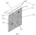
- FIG. 1 there is shown an anode hanger bar 100, supporting two anode meshes mechanically connected to a support structure of five vertical bars 110.
- the frontal anode mesh 101 which partially hides the posterior anode mesh (not referenced), is subdivided into 100 sub-meshes, such as sub-mesh 102.
- electrical connection cables 103 Also shown are electrical connection cables 103, the insulation gap 104 between sub-meshes, and cathode 106.
- the electronic system of current adjustment can be placed in correspondence of location 1051.
- the electronic system of current adjustment can be placed directly in correspondence of the sub-mesh to be controlled, such as position 1052 for sub-mesh 102.
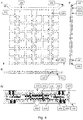
- FIG 2 there is shown a schematic diagram of an active electric microcircuit indicating the area corresponding to the electronic system circuit 105, connected to sub-mesh 102 via the relevant connection cable 103, on one side, and to the anode hanger bar 100 on the other side.
- the active electronic system circuit 105 comprises a resistor 109 and a combination of control 107 and active component 108.
- the latter component may be, for example, a transistor, a MOSFET, a switch transistor or a load switch.
- Elements 107 and 108 can compare the drop of voltage at the resistor with a predefined reference voltage; when the resistor drop of voltage is bigger than the voltage reference for a preset period of time, element 107 triggers the gate lock of element 108.
- FIG 3 there is shown a diagram of a passive electric system indicating the area corresponding to the passive electronic device 101, which can be a positive temperature coefficient thermistor or resettable fuse, connected to sub-mesh 102 via the relevant connection cable 103, on one side, and the anode hanger bar 100 on the other.
- the passive electronic device 101 which can be a positive temperature coefficient thermistor or resettable fuse
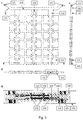
- panels I and II show, respectively, a front and side view of an anodic structure implementing passive current probe and control components comprising electrically conductive hanger bar 100 with terminal contacts 101, and two anode meshes each divided into 36 sub-meshes, such as sub-mesh 102.
- Sub-mesh 102 is connected to the supporting means 110 through conductive and chemically resistant rivets 300, which can be made, for example, of titanium or alloys thereof.
- Panel III shows the cross section of the anodic structure of Panel I taken along the dash-dotted line. The region enclosed in the dashed area comprising supporting means 110 and sub-mesh 102 is enlarged in panel IV, which shows a blow-up of the connection between sub-mesh 102 and the supporting means 110.
- the supporting means 110 which are electrically connected to the anode hanger bar (not shown), comprise conductive bar 500, which is fixed to printed circuit board 450 via rivets 350.
- Conductive bar 500 is connected to one pin of Polyfuse 410 via printed circuit board track 550.
- the second pin of Polyfuse 410 is in electrical contact with sub-mesh 102 through rivet 300.
- Polyfuse 410 is enclosed in thermally insulating region 250 (which can be filled, for example, with thermally insulating foam or air).
- An overlay of electrically insulating and chemical resistant material 200 seals, insulates and protects from the electrolyte the above mentioned components and circuits with the exception of rivet 300, which partially emerges from the supporting means and secures sub-mesh 102 to structure 110.
- panels I and II show, respectively, a front and side view of an anodic structure implementing active current control components comprising electrically conductive hanger bar 100 with terminal contacts 101, and two anode meshes consisting of 6x6 sub-meshes, such as sub-mesh 102.
- the anodic structure further comprises at least one MCU 130.
- Cable connection 120 connects the MCU to the cathodic intercell bar or on the cathodic balance bar, if any, on one side, and to the hanger bar 100, on the other side (connections not shown).
- Sub-mesh 102 is connected to the supporting means 110 through conductive and chemically resistant rivets 300, which can be made, for example, of titanium or alloys thereof.
- Panel III shows the cross section of the anodic structure of Panel I taken along the dash-dotted line.
- the region enclosed in the dashed area comprising supporting means 110 and sub-mesh 102 is enlarged in panel IV.
- Panel IV shows a blow-up of the connection between sub-mesh 102 and the supporting means 110.
- the supporting means 110 which are electrically connected to the anode hanger bar (not shown), comprise conductive bar 500, which is fixed to printed circuit board 450 via rivets 350.
- Conductive bar 500 is connected to one terminal of transistor 420 via printed circuit board track 550.
- Transistor 420 is further connected with shunt resistance 430, which is in electrical contact with sub-mesh 102 via rivet 300.
- connection between the shunt resistance 430 and the MCU 130, and the connection between the latter and the gate of transistor 420 are not shown in figure. These connections respectively carry the input and output signals to/from the MCU, which can be equipped with an analog to digital converter (not shown).
- Transistor 420 and shunt resistance 430 can be connected according to the diagram of Figure 2 to an additional control transistor (not shown).
- a laboratory test campaign was carried out inside an electrowinning cell, containing a cathode and an anode equipped with an active current control electronic system.
- a 3 mm thick, 50 mm wide and 1000 mm high AISI 316 stainless steel sheet was used as the cathode;
- the anode consisted of a 2 mm thick, 150 mm wide and 1000 mm high titanium expanded mesh, activated with a coating of mixed oxides of iridium and tantalum, subdivided into sub-meshes of 1 dm 2 each.
- the cathode and the anode were vertically facing each other with a gap of 40 mm between the outer surfaces.
- a dendrite was produced artificially by inserting a screw, as a nucleation centre, into the stainless steel plate perpendicularly to the anode, the tip of the screw being spaced 4 mm apart from the anode.
- Each sub-mesh was electrically connected to the anode hanger bar and to the electronic system according to the diagram of Figure 2 .
- the electronic system comprised two different MOSFET transistors, one working as the power switch 108, and the other as controller 107.
- the power switch was characterised by a drain-source breakdown voltage of -30V, and an on resistance of 8 m ⁇ at a gate threshold voltage of -10V.
- the controller transistor was characterised by a drain-source breakdown voltage of -30V, and an on resistance of 85 m ⁇ at a gate threshold voltage of 4.5 V. In place of resistor 109 of Figure 2 , a shunt resistance of 2 m ⁇ was used.
- a 32-bit, 67 MHz MCU recorded the current values of each sub-mesh at time intervals of 1 milliseconds, calculating the relative deviation from the average current of each sub-mesh. The MCU was programmed to interrupt the current in the sub-meshes where the relative deviation exceeded 5%.
- a wireless ZigBee radio communication system was installed on the anode and sent the information collected by the MCU to a main control computer, for managing and alert purposes. After 4 days of operation a lateral growth of copper was evidenced on the dendrite, not reaching the anode surface. The production of copper in the areas facing the remaining sub-meshes showed no irregularities.
- Example 1 The anodic structure of Example 1 was tested in the same conditions without activating the electronic control system. The dendrite reached the anode surface after 4 hours of operation, irreparably damaging the anode.
- a laboratory test campaign was carried out in a laboratory cell simulating an electrowinning cell, containing a cathode and an anodic structure equipped with a passive current control electronic system.
- a 3 mm thick, 150 mm wide and 1000 mm high AISI 316 stainless steel sheet was used as cathode; the anode consisted of a 180 mm long copper hanger bar, 20 mm wide and 40 mm high, and of a 1 mm thick, 155 mm wide and 1030 mm high titanium expanded mesh, activated with a coating of mixed oxides of iridium, subdivided into 18 sub-meshes, each 75 mm wide and 110 mm high, with a gap of 8 mm between each couple of sub-meshes.
- the anodic structure was also equipped with a LED, a ZigBee radio communication device and a booster with an output voltage of 3.3 V.
- the booster was used to power the LED and ZigBee device, which were installed for alert and operation managing purposes.
- Each sub-mesh was electrically connected to the anode hanger bar and to the electronic system according to the diagram of Figure 3 . More specifically, the electronic system comprised a positive temperature coefficient polyfuse characterised by a hold and trip current specifications at 23°C of 14.0 A and 23.8 A respectively (a temperature dependent characterization of these parameters was carried out by the inventor in order to assess and verify the polyfuse performance at the operating temperatures of the cell.
- the hold current at 40 °C was 12.2 A and the trip current was 25.4 A).
- Each sub-mesh was further connected to a diode.
- the total of 18 diodes were connected to form a diode-OR circuit that supplied power to the booster and only activated the LED in case of electrical contact between one or more sub-meshes and the cathode.
- the cathode and the anode were vertically facing each other with a gap of 35 mm between the outer surfaces.
- a dendrite was produced artificially by inserting a screw, as a nucleation centre, into the cathodic stainless steel plate perpendicularly to the anode mesh; the tip of the screw being spaced 4 mm apart from the anode.
- the copper deposited on the tip of the screw would contact the facing anode submesh, resulting in a copper deposition on the specific submesh, the lighting up of the LED and a warning signal from the ZigBee communication device to a main central computer.
Landscapes
- Chemical & Material Sciences (AREA)
- Engineering & Computer Science (AREA)
- Chemical Kinetics & Catalysis (AREA)
- Electrochemistry (AREA)
- Materials Engineering (AREA)
- Metallurgy (AREA)
- Organic Chemistry (AREA)
- Electrolytic Production Of Metals (AREA)
- Electroplating Methods And Accessories (AREA)
- Prevention Of Electric Corrosion (AREA)
Priority Applications (1)
| Application Number | Priority Date | Filing Date | Title |
|---|---|---|---|
| PL15703939T PL3108037T3 (pl) | 2014-02-19 | 2015-02-03 | Struktura anodowa dla ogniw dla elektrolitycznego otrzymywania metali |
Applications Claiming Priority (2)
| Application Number | Priority Date | Filing Date | Title |
|---|---|---|---|
| ITMI20140238 | 2014-02-19 | ||
| PCT/EP2015/052122 WO2015079072A2 (en) | 2014-02-19 | 2015-02-03 | Anode structure for metal electrowinning cells |
Publications (2)
| Publication Number | Publication Date |
|---|---|
| EP3108037A2 EP3108037A2 (en) | 2016-12-28 |
| EP3108037B1 true EP3108037B1 (en) | 2018-04-18 |
Family
ID=50336465
Family Applications (1)
| Application Number | Title | Priority Date | Filing Date |
|---|---|---|---|
| EP15703939.7A Active EP3108037B1 (en) | 2014-02-19 | 2015-02-03 | Anode structure for metal electrowinning cells |
Country Status (17)
| Country | Link |
|---|---|
| US (1) | US10309023B2 (es) |
| EP (1) | EP3108037B1 (es) |
| JP (1) | JP6580057B2 (es) |
| KR (1) | KR102281669B1 (es) |
| CN (1) | CN106034404B (es) |
| AP (1) | AP2016009431A0 (es) |
| AU (1) | AU2015203062B2 (es) |
| BR (1) | BR112016019065B1 (es) |
| CA (1) | CA2939337C (es) |
| CL (1) | CL2016000367A1 (es) |
| EA (1) | EA030372B1 (es) |
| ES (1) | ES2679595T3 (es) |
| PE (1) | PE20161107A1 (es) |
| PH (1) | PH12016501660A1 (es) |
| PL (1) | PL3108037T3 (es) |
| TW (1) | TWI655324B (es) |
| WO (1) | WO2015079072A2 (es) |
Families Citing this family (8)
| Publication number | Priority date | Publication date | Assignee | Title |
|---|---|---|---|---|
| ITUB20151809A1 (it) * | 2015-07-01 | 2017-01-01 | Industrie De Nora Spa | Struttura di elettrodo per elettrodeposizione di metalli non ferrosi |
| IT201600083106A1 (it) * | 2016-08-05 | 2018-02-05 | Industrie De Nora Spa | Struttura di elettrodo provvista di resistori |
| ITUA20161470A1 (it) * | 2016-03-09 | 2017-09-09 | Industrie De Nora Spa | Struttura di elettrodo provvista di resistori |
| US11136684B2 (en) * | 2016-03-09 | 2021-10-05 | Industrie De Nora S.P.A. | Electrode structure provided with resistors |
| ES2580552B1 (es) * | 2016-04-29 | 2017-05-31 | Industrie De Nora S.P.A. | Ánodo seguro para celda electroquímica. |
| KR101819219B1 (ko) * | 2017-02-27 | 2018-01-16 | (주) 테크윈 | 전해 제련용 양극 구조체, 이의 제조 방법 및 이를 포함하는 전해 제련 장지 |
| KR102017567B1 (ko) * | 2018-11-27 | 2019-09-03 | 주식회사 웨스코일렉트로드 | 전해 제련용 전극 조립체 |
| CN110499519B (zh) * | 2019-06-11 | 2021-06-15 | 内蒙古锦联铝材有限公司 | 一种焦粒焙烧分流方法 |
Family Cites Families (31)
| Publication number | Priority date | Publication date | Assignee | Title |
|---|---|---|---|---|
| JPS502378B1 (es) * | 1969-02-26 | 1975-01-25 | ||
| AU527416B2 (en) * | 1980-07-26 | 1983-03-03 | Peter Berger | Electrode edge protectors |
| DE3406797C2 (de) * | 1984-02-24 | 1985-12-19 | Conradty GmbH & Co Metallelektroden KG, 8505 Röthenbach | Beschichtete Ventilmetallanode zur elektrolytischen Gewinnung von Metallen oder Metalloxiden |
| DE3421480A1 (de) * | 1984-06-08 | 1985-12-12 | Conradty GmbH & Co Metallelektroden KG, 8505 Röthenbach | Beschichtete ventilmetall-elektrode zur elektrolytischen galvanisierung |
| JPS6123797A (ja) * | 1984-07-09 | 1986-02-01 | Katsukawa Kogyo Kk | 電解装置における電極体 |
| US4935108A (en) * | 1989-04-28 | 1990-06-19 | Hewlett-Packard Company | Apparatus for troubleshooting photoimage plating problems in printed circuit board manufacturing |
| JP2506573B2 (ja) * | 1990-12-19 | 1996-06-12 | 日鉱グールド・フォイル株式会社 | 電解銅箔の製造方法及び装置 |
| US5100525A (en) * | 1990-07-25 | 1992-03-31 | Eltech Systems Corporation | Spring supported anode |
| EP0491163B1 (en) * | 1990-12-19 | 1996-02-14 | Nikko Gould Foil Co., Ltd. | Method and apparatus for producing electrolytic copper foil |
| US5326455A (en) * | 1990-12-19 | 1994-07-05 | Nikko Gould Foil Co., Ltd. | Method of producing electrolytic copper foil and apparatus for producing same |
| JP2774209B2 (ja) * | 1991-12-26 | 1998-07-09 | ペルメレック電極株式会社 | 金属箔連続製造装置用の陽極 |
| US5882491A (en) * | 1996-01-02 | 1999-03-16 | Skf Industrial Trading & Development Company B.V. | Electrode for electrochemical machining, method of electrochemical machining with said electrode, a bearing and a method of determining a profile using said electrode |
| JP3180902B2 (ja) * | 1998-05-19 | 2001-07-03 | 日鉱金属株式会社 | 電解製錬における異常電極の検出方法及び異常電極検出システム |
| US6153328A (en) * | 1999-11-24 | 2000-11-28 | Metallic Power, Inc. | System and method for preventing the formation of dendrites in a metal/air fuel cell, battery or metal recovery apparatus |
| JP2001192879A (ja) * | 2000-01-13 | 2001-07-17 | Sumitomo Metal Mining Co Ltd | 電気銅製造用の種板成形ロールおよびそれを用いて成形された電気銅製造用の種板、ならびに該種板を用いて電気銅を製造する方法および該方法により得られた電気銅 |
| TWI277473B (en) * | 2002-01-31 | 2007-04-01 | Ebara Corp | Electrolytic processing apparatus and method, fixing method, fixing structure for ion exchanging member |
| JP2007224321A (ja) * | 2006-02-21 | 2007-09-06 | Think Laboratory Co Ltd | シリンダ用メッキ方法及び装置 |
| CN101849039B (zh) * | 2007-07-31 | 2013-04-10 | 恩克泰克敏股份公司 | 用于监测、控制和管理用于实施有色金属的湿法冶金电解提取和电解精炼过程的设备的系统 |
| KR100956683B1 (ko) * | 2007-09-20 | 2010-05-10 | 삼성전기주식회사 | 수소발생장치의 전극연결방법 및 그것을 이용한수소발생장치 |
| WO2009040250A2 (de) * | 2007-09-20 | 2009-04-02 | Siemens Aktiengesellschaft | Stromsteuerungsvorrichtung eines stromnetzes einer elektrochemischen beschichtungsanlage |
| EP2184385A2 (de) * | 2008-10-30 | 2010-05-12 | IP Bewertungs AG | Elektrode und Verfahren für eine elektrolytische Schichtabscheidung |
| US8440355B2 (en) * | 2010-01-21 | 2013-05-14 | Tai-Her Yang | Equalizing electrode plate with insulated split-flow conductive structure |
| US8152987B2 (en) * | 2010-04-02 | 2012-04-10 | Recherche 2000 Inc. | Method for ensuring and monitoring electrolyzer safety and performances |
| PL410260A1 (pl) * | 2010-08-11 | 2015-05-11 | Outotec Oyj | Urządzenie do elektroprodukcji |
| ITMI20111668A1 (it) * | 2011-09-16 | 2013-03-17 | Industrie De Nora Spa | Sistema permanente per la valutazione in continuo della distribuzione di corrente in celle elettrolitiche interconnesse. |
| ITMI20111938A1 (it) * | 2011-10-26 | 2013-04-27 | Industrie De Nora Spa | Comparto anodico per celle per estrazione elettrolitica di metalli |
| PL397081A1 (pl) * | 2011-11-22 | 2013-05-27 | Nano-Tech Spólka Z Ograniczona Odpowiedzialnoscia | Sposób elektrorafinacji miedzi |
| CN202595298U (zh) * | 2012-03-23 | 2012-12-12 | 宝钛特种金属有限公司 | 电解金属用钛网涂层阳极 |
| ITMI20130505A1 (it) * | 2013-04-04 | 2014-10-05 | Industrie De Nora Spa | Cella per estrazione elettrolitica di metalli |
| CN203999855U (zh) * | 2014-03-10 | 2014-12-10 | 浙江蓝博金属科技有限公司 | 一种电解板 |
| CN104372376A (zh) * | 2014-06-20 | 2015-02-25 | 商实企业有限公司 | 从棕化废液中回收铜的方法 |
-
2015
- 2015-01-30 TW TW104103108A patent/TWI655324B/zh active
- 2015-02-03 ES ES15703939.7T patent/ES2679595T3/es active Active
- 2015-02-03 EP EP15703939.7A patent/EP3108037B1/en active Active
- 2015-02-03 JP JP2016553342A patent/JP6580057B2/ja active Active
- 2015-02-03 PL PL15703939T patent/PL3108037T3/pl unknown
- 2015-02-03 PE PE2016001496A patent/PE20161107A1/es unknown
- 2015-02-03 BR BR112016019065-3A patent/BR112016019065B1/pt active IP Right Grant
- 2015-02-03 US US15/119,266 patent/US10309023B2/en active Active
- 2015-02-03 CA CA2939337A patent/CA2939337C/en active Active
- 2015-02-03 KR KR1020167025500A patent/KR102281669B1/ko active IP Right Grant
- 2015-02-03 CN CN201580009410.5A patent/CN106034404B/zh active Active
- 2015-02-03 EA EA201691667A patent/EA030372B1/ru not_active IP Right Cessation
- 2015-02-03 AP AP2016009431A patent/AP2016009431A0/en unknown
- 2015-02-03 WO PCT/EP2015/052122 patent/WO2015079072A2/en active Application Filing
- 2015-02-03 AU AU2015203062A patent/AU2015203062B2/en active Active
-
2016
- 2016-02-18 CL CL2016000367A patent/CL2016000367A1/es unknown
- 2016-08-19 PH PH12016501660A patent/PH12016501660A1/en unknown
Non-Patent Citations (1)
| Title |
|---|
| None * |
Also Published As
| Publication number | Publication date |
|---|---|
| US10309023B2 (en) | 2019-06-04 |
| TW201546332A (zh) | 2015-12-16 |
| EA201691667A1 (ru) | 2016-11-30 |
| JP6580057B2 (ja) | 2019-09-25 |
| JP2017511428A (ja) | 2017-04-20 |
| EP3108037A2 (en) | 2016-12-28 |
| CN106034404B (zh) | 2018-07-03 |
| PL3108037T3 (pl) | 2018-12-31 |
| WO2015079072A2 (en) | 2015-06-04 |
| US20170009359A1 (en) | 2017-01-12 |
| CL2016000367A1 (es) | 2016-08-12 |
| CN106034404A (zh) | 2016-10-19 |
| KR102281669B1 (ko) | 2021-07-30 |
| BR112016019065B1 (pt) | 2022-03-29 |
| ES2679595T3 (es) | 2018-08-29 |
| WO2015079072A3 (en) | 2015-07-23 |
| AP2016009431A0 (en) | 2016-09-30 |
| PH12016501660B1 (en) | 2016-11-07 |
| PE20161107A1 (es) | 2016-11-24 |
| CA2939337A1 (en) | 2015-06-04 |
| KR20160122826A (ko) | 2016-10-24 |
| BR112016019065A2 (es) | 2017-08-15 |
| AU2015203062A1 (en) | 2016-08-18 |
| AU2015203062B2 (en) | 2018-12-13 |
| TWI655324B (zh) | 2019-04-01 |
| CA2939337C (en) | 2022-03-08 |
| PH12016501660A1 (en) | 2016-11-07 |
| EA030372B1 (ru) | 2018-07-31 |
Similar Documents
| Publication | Publication Date | Title |
|---|---|---|
| EP3108037B1 (en) | Anode structure for metal electrowinning cells | |
| PH12015502286B1 (en) | Electrolytic cell for metal electrowinning | |
| EP3175020B1 (en) | Cell for metal electrowinning | |
| US10400344B2 (en) | Apparatus for protection of anodes and cathodes in a system of electrolysis cells | |
| US20220200263A1 (en) | Short-circuit mitigation device | |
| EP3426824B1 (en) | Electrode structure provided with resistors |
Legal Events
| Date | Code | Title | Description |
|---|---|---|---|
| PUAI | Public reference made under article 153(3) epc to a published international application that has entered the european phase |
Free format text: ORIGINAL CODE: 0009012 |
|
| STAA | Information on the status of an ep patent application or granted ep patent |
Free format text: STATUS: REQUEST FOR EXAMINATION WAS MADE |
|
| 17P | Request for examination filed |
Effective date: 20160818 |
|
| AK | Designated contracting states |
Kind code of ref document: A2 Designated state(s): AL AT BE BG CH CY CZ DE DK EE ES FI FR GB GR HR HU IE IS IT LI LT LU LV MC MK MT NL NO PL PT RO RS SE SI SK SM TR |
|
| AX | Request for extension of the european patent |
Extension state: BA ME |
|
| DAX | Request for extension of the european patent (deleted) | ||
| GRAP | Despatch of communication of intention to grant a patent |
Free format text: ORIGINAL CODE: EPIDOSNIGR1 |
|
| STAA | Information on the status of an ep patent application or granted ep patent |
Free format text: STATUS: GRANT OF PATENT IS INTENDED |
|
| RIC1 | Information provided on ipc code assigned before grant |
Ipc: C25C 7/06 20060101ALI20171013BHEP Ipc: C25C 1/12 20060101ALI20171013BHEP Ipc: C25C 1/00 20060101AFI20171013BHEP Ipc: C25C 7/02 20060101ALI20171013BHEP |
|
| INTG | Intention to grant announced |
Effective date: 20171106 |
|
| GRAS | Grant fee paid |
Free format text: ORIGINAL CODE: EPIDOSNIGR3 |
|
| GRAA | (expected) grant |
Free format text: ORIGINAL CODE: 0009210 |
|
| STAA | Information on the status of an ep patent application or granted ep patent |
Free format text: STATUS: THE PATENT HAS BEEN GRANTED |
|
| AK | Designated contracting states |
Kind code of ref document: B1 Designated state(s): AL AT BE BG CH CY CZ DE DK EE ES FI FR GB GR HR HU IE IS IT LI LT LU LV MC MK MT NL NO PL PT RO RS SE SI SK SM TR |
|
| REG | Reference to a national code |
Ref country code: GB Ref legal event code: FG4D |
|
| REG | Reference to a national code |
Ref country code: CH Ref legal event code: EP |
|
| REG | Reference to a national code |
Ref country code: DE Ref legal event code: R096 Ref document number: 602015010104 Country of ref document: DE |
|
| REG | Reference to a national code |
Ref country code: AT Ref legal event code: REF Ref document number: 990568 Country of ref document: AT Kind code of ref document: T Effective date: 20180515 |
|
| REG | Reference to a national code |
Ref country code: IE Ref legal event code: FG4D |
|
| REG | Reference to a national code |
Ref country code: CH Ref legal event code: NV Representative=s name: FIAMMENGHI-FIAMMENGHI, CH |
|
| REG | Reference to a national code |
Ref country code: NL Ref legal event code: FP |
|
| REG | Reference to a national code |
Ref country code: SE Ref legal event code: TRGR |
|
| REG | Reference to a national code |
Ref country code: ES Ref legal event code: FG2A Ref document number: 2679595 Country of ref document: ES Kind code of ref document: T3 Effective date: 20180829 |
|
| REG | Reference to a national code |
Ref country code: LT Ref legal event code: MG4D |
|
| REG | Reference to a national code |
Ref country code: NO Ref legal event code: T2 Effective date: 20180418 |
|
| PG25 | Lapsed in a contracting state [announced via postgrant information from national office to epo] |
Ref country code: LT Free format text: LAPSE BECAUSE OF FAILURE TO SUBMIT A TRANSLATION OF THE DESCRIPTION OR TO PAY THE FEE WITHIN THE PRESCRIBED TIME-LIMIT Effective date: 20180418 Ref country code: AL Free format text: LAPSE BECAUSE OF FAILURE TO SUBMIT A TRANSLATION OF THE DESCRIPTION OR TO PAY THE FEE WITHIN THE PRESCRIBED TIME-LIMIT Effective date: 20180418 Ref country code: BG Free format text: LAPSE BECAUSE OF FAILURE TO SUBMIT A TRANSLATION OF THE DESCRIPTION OR TO PAY THE FEE WITHIN THE PRESCRIBED TIME-LIMIT Effective date: 20180718 |
|
| PG25 | Lapsed in a contracting state [announced via postgrant information from national office to epo] |
Ref country code: RS Free format text: LAPSE BECAUSE OF FAILURE TO SUBMIT A TRANSLATION OF THE DESCRIPTION OR TO PAY THE FEE WITHIN THE PRESCRIBED TIME-LIMIT Effective date: 20180418 Ref country code: LV Free format text: LAPSE BECAUSE OF FAILURE TO SUBMIT A TRANSLATION OF THE DESCRIPTION OR TO PAY THE FEE WITHIN THE PRESCRIBED TIME-LIMIT Effective date: 20180418 Ref country code: GR Free format text: LAPSE BECAUSE OF FAILURE TO SUBMIT A TRANSLATION OF THE DESCRIPTION OR TO PAY THE FEE WITHIN THE PRESCRIBED TIME-LIMIT Effective date: 20180719 Ref country code: HR Free format text: LAPSE BECAUSE OF FAILURE TO SUBMIT A TRANSLATION OF THE DESCRIPTION OR TO PAY THE FEE WITHIN THE PRESCRIBED TIME-LIMIT Effective date: 20180418 |
|
| REG | Reference to a national code |
Ref country code: AT Ref legal event code: MK05 Ref document number: 990568 Country of ref document: AT Kind code of ref document: T Effective date: 20180418 |
|
| REG | Reference to a national code |
Ref country code: DE Ref legal event code: R097 Ref document number: 602015010104 Country of ref document: DE |
|
| PG25 | Lapsed in a contracting state [announced via postgrant information from national office to epo] |
Ref country code: AT Free format text: LAPSE BECAUSE OF FAILURE TO SUBMIT A TRANSLATION OF THE DESCRIPTION OR TO PAY THE FEE WITHIN THE PRESCRIBED TIME-LIMIT Effective date: 20180418 Ref country code: EE Free format text: LAPSE BECAUSE OF FAILURE TO SUBMIT A TRANSLATION OF THE DESCRIPTION OR TO PAY THE FEE WITHIN THE PRESCRIBED TIME-LIMIT Effective date: 20180418 Ref country code: DK Free format text: LAPSE BECAUSE OF FAILURE TO SUBMIT A TRANSLATION OF THE DESCRIPTION OR TO PAY THE FEE WITHIN THE PRESCRIBED TIME-LIMIT Effective date: 20180418 Ref country code: SK Free format text: LAPSE BECAUSE OF FAILURE TO SUBMIT A TRANSLATION OF THE DESCRIPTION OR TO PAY THE FEE WITHIN THE PRESCRIBED TIME-LIMIT Effective date: 20180418 Ref country code: RO Free format text: LAPSE BECAUSE OF FAILURE TO SUBMIT A TRANSLATION OF THE DESCRIPTION OR TO PAY THE FEE WITHIN THE PRESCRIBED TIME-LIMIT Effective date: 20180418 Ref country code: CZ Free format text: LAPSE BECAUSE OF FAILURE TO SUBMIT A TRANSLATION OF THE DESCRIPTION OR TO PAY THE FEE WITHIN THE PRESCRIBED TIME-LIMIT Effective date: 20180418 |
|
| PLBE | No opposition filed within time limit |
Free format text: ORIGINAL CODE: 0009261 |
|
| STAA | Information on the status of an ep patent application or granted ep patent |
Free format text: STATUS: NO OPPOSITION FILED WITHIN TIME LIMIT |
|
| PG25 | Lapsed in a contracting state [announced via postgrant information from national office to epo] |
Ref country code: SM Free format text: LAPSE BECAUSE OF FAILURE TO SUBMIT A TRANSLATION OF THE DESCRIPTION OR TO PAY THE FEE WITHIN THE PRESCRIBED TIME-LIMIT Effective date: 20180418 |
|
| 26N | No opposition filed |
Effective date: 20190121 |
|
| PG25 | Lapsed in a contracting state [announced via postgrant information from national office to epo] |
Ref country code: SI Free format text: LAPSE BECAUSE OF FAILURE TO SUBMIT A TRANSLATION OF THE DESCRIPTION OR TO PAY THE FEE WITHIN THE PRESCRIBED TIME-LIMIT Effective date: 20180418 |
|
| PG25 | Lapsed in a contracting state [announced via postgrant information from national office to epo] |
Ref country code: LU Free format text: LAPSE BECAUSE OF NON-PAYMENT OF DUE FEES Effective date: 20190203 Ref country code: MC Free format text: LAPSE BECAUSE OF FAILURE TO SUBMIT A TRANSLATION OF THE DESCRIPTION OR TO PAY THE FEE WITHIN THE PRESCRIBED TIME-LIMIT Effective date: 20180418 |
|
| REG | Reference to a national code |
Ref country code: IE Ref legal event code: MM4A |
|
| PG25 | Lapsed in a contracting state [announced via postgrant information from national office to epo] |
Ref country code: IE Free format text: LAPSE BECAUSE OF NON-PAYMENT OF DUE FEES Effective date: 20190203 |
|
| PG25 | Lapsed in a contracting state [announced via postgrant information from national office to epo] |
Ref country code: TR Free format text: LAPSE BECAUSE OF FAILURE TO SUBMIT A TRANSLATION OF THE DESCRIPTION OR TO PAY THE FEE WITHIN THE PRESCRIBED TIME-LIMIT Effective date: 20180418 |
|
| PG25 | Lapsed in a contracting state [announced via postgrant information from national office to epo] |
Ref country code: PT Free format text: LAPSE BECAUSE OF FAILURE TO SUBMIT A TRANSLATION OF THE DESCRIPTION OR TO PAY THE FEE WITHIN THE PRESCRIBED TIME-LIMIT Effective date: 20180820 Ref country code: MT Free format text: LAPSE BECAUSE OF NON-PAYMENT OF DUE FEES Effective date: 20190203 |
|
| PGFP | Annual fee paid to national office [announced via postgrant information from national office to epo] |
Ref country code: CH Payment date: 20210217 Year of fee payment: 7 |
|
| PG25 | Lapsed in a contracting state [announced via postgrant information from national office to epo] |
Ref country code: CY Free format text: LAPSE BECAUSE OF FAILURE TO SUBMIT A TRANSLATION OF THE DESCRIPTION OR TO PAY THE FEE WITHIN THE PRESCRIBED TIME-LIMIT Effective date: 20180418 |
|
| PG25 | Lapsed in a contracting state [announced via postgrant information from national office to epo] |
Ref country code: IS Free format text: LAPSE BECAUSE OF FAILURE TO SUBMIT A TRANSLATION OF THE DESCRIPTION OR TO PAY THE FEE WITHIN THE PRESCRIBED TIME-LIMIT Effective date: 20180818 |
|
| PG25 | Lapsed in a contracting state [announced via postgrant information from national office to epo] |
Ref country code: HU Free format text: LAPSE BECAUSE OF FAILURE TO SUBMIT A TRANSLATION OF THE DESCRIPTION OR TO PAY THE FEE WITHIN THE PRESCRIBED TIME-LIMIT; INVALID AB INITIO Effective date: 20150203 |
|
| PG25 | Lapsed in a contracting state [announced via postgrant information from national office to epo] |
Ref country code: MK Free format text: LAPSE BECAUSE OF FAILURE TO SUBMIT A TRANSLATION OF THE DESCRIPTION OR TO PAY THE FEE WITHIN THE PRESCRIBED TIME-LIMIT Effective date: 20180418 |
|
| REG | Reference to a national code |
Ref country code: CH Ref legal event code: PL |
|
| PG25 | Lapsed in a contracting state [announced via postgrant information from national office to epo] |
Ref country code: LI Free format text: LAPSE BECAUSE OF NON-PAYMENT OF DUE FEES Effective date: 20220228 Ref country code: CH Free format text: LAPSE BECAUSE OF NON-PAYMENT OF DUE FEES Effective date: 20220228 |
|
| PGFP | Annual fee paid to national office [announced via postgrant information from national office to epo] |
Ref country code: NO Payment date: 20230220 Year of fee payment: 9 Ref country code: FR Payment date: 20230221 Year of fee payment: 9 |
|
| PGFP | Annual fee paid to national office [announced via postgrant information from national office to epo] |
Ref country code: SE Payment date: 20230216 Year of fee payment: 9 Ref country code: PL Payment date: 20230127 Year of fee payment: 9 Ref country code: IT Payment date: 20230223 Year of fee payment: 9 Ref country code: BE Payment date: 20230216 Year of fee payment: 9 |
|
| P01 | Opt-out of the competence of the unified patent court (upc) registered |
Effective date: 20230526 |
|
| PGFP | Annual fee paid to national office [announced via postgrant information from national office to epo] |
Ref country code: ES Payment date: 20240326 Year of fee payment: 10 Ref country code: NL Payment date: 20240219 Year of fee payment: 10 |
|
| PGFP | Annual fee paid to national office [announced via postgrant information from national office to epo] |
Ref country code: FI Payment date: 20240219 Year of fee payment: 10 Ref country code: DE Payment date: 20240219 Year of fee payment: 10 Ref country code: GB Payment date: 20240219 Year of fee payment: 10 |