EP3104397B1 - Verfahren zur dotierung von siliciumwafern - Google Patents
Verfahren zur dotierung von siliciumwafern Download PDFInfo
- Publication number
- EP3104397B1 EP3104397B1 EP15171263.5A EP15171263A EP3104397B1 EP 3104397 B1 EP3104397 B1 EP 3104397B1 EP 15171263 A EP15171263 A EP 15171263A EP 3104397 B1 EP3104397 B1 EP 3104397B1
- Authority
- EP
- European Patent Office
- Prior art keywords
- gas
- flow rate
- doping
- ratio
- silicon wafers
- Prior art date
- Legal status (The legal status is an assumption and is not a legal conclusion. Google has not performed a legal analysis and makes no representation as to the accuracy of the status listed.)
- Active
Links
Images

Classifications
-
- H—ELECTRICITY
- H10—SEMICONDUCTOR DEVICES; ELECTRIC SOLID-STATE DEVICES NOT OTHERWISE PROVIDED FOR
- H10P—GENERIC PROCESSES OR APPARATUS FOR THE MANUFACTURE OR TREATMENT OF DEVICES COVERED BY CLASS H10
- H10P32/00—Diffusion of dopants within, into or out of wafers, substrates or parts of devices
- H10P32/10—Diffusion of dopants within, into or out of semiconductor bodies or layers
- H10P32/14—Diffusion of dopants within, into or out of semiconductor bodies or layers within a single semiconductor body or layer in a solid phase; between different semiconductor bodies or layers, both in a solid phase
- H10P32/1404—Diffusion of dopants within, into or out of semiconductor bodies or layers within a single semiconductor body or layer in a solid phase; between different semiconductor bodies or layers, both in a solid phase using predeposition followed by drive-in of impurities into the semiconductor surface, e.g. predeposition from a gaseous phase
-
- H—ELECTRICITY
- H10—SEMICONDUCTOR DEVICES; ELECTRIC SOLID-STATE DEVICES NOT OTHERWISE PROVIDED FOR
- H10F—INORGANIC SEMICONDUCTOR DEVICES SENSITIVE TO INFRARED RADIATION, LIGHT, ELECTROMAGNETIC RADIATION OF SHORTER WAVELENGTH OR CORPUSCULAR RADIATION
- H10F71/00—Manufacture or treatment of devices covered by this subclass
- H10F71/121—The active layers comprising only Group IV materials
-
- H—ELECTRICITY
- H10—SEMICONDUCTOR DEVICES; ELECTRIC SOLID-STATE DEVICES NOT OTHERWISE PROVIDED FOR
- H10P—GENERIC PROCESSES OR APPARATUS FOR THE MANUFACTURE OR TREATMENT OF DEVICES COVERED BY CLASS H10
- H10P32/00—Diffusion of dopants within, into or out of wafers, substrates or parts of devices
- H10P32/10—Diffusion of dopants within, into or out of semiconductor bodies or layers
- H10P32/17—Diffusion of dopants within, into or out of semiconductor bodies or layers characterised by the semiconductor material
- H10P32/171—Diffusion of dopants within, into or out of semiconductor bodies or layers characterised by the semiconductor material being group IV material
-
- Y—GENERAL TAGGING OF NEW TECHNOLOGICAL DEVELOPMENTS; GENERAL TAGGING OF CROSS-SECTIONAL TECHNOLOGIES SPANNING OVER SEVERAL SECTIONS OF THE IPC; TECHNICAL SUBJECTS COVERED BY FORMER USPC CROSS-REFERENCE ART COLLECTIONS [XRACs] AND DIGESTS
- Y02—TECHNOLOGIES OR APPLICATIONS FOR MITIGATION OR ADAPTATION AGAINST CLIMATE CHANGE
- Y02E—REDUCTION OF GREENHOUSE GAS [GHG] EMISSIONS, RELATED TO ENERGY GENERATION, TRANSMISSION OR DISTRIBUTION
- Y02E10/00—Energy generation through renewable energy sources
- Y02E10/50—Photovoltaic [PV] energy
- Y02E10/547—Monocrystalline silicon PV cells
-
- Y—GENERAL TAGGING OF NEW TECHNOLOGICAL DEVELOPMENTS; GENERAL TAGGING OF CROSS-SECTIONAL TECHNOLOGIES SPANNING OVER SEVERAL SECTIONS OF THE IPC; TECHNICAL SUBJECTS COVERED BY FORMER USPC CROSS-REFERENCE ART COLLECTIONS [XRACs] AND DIGESTS
- Y02—TECHNOLOGIES OR APPLICATIONS FOR MITIGATION OR ADAPTATION AGAINST CLIMATE CHANGE
- Y02P—CLIMATE CHANGE MITIGATION TECHNOLOGIES IN THE PRODUCTION OR PROCESSING OF GOODS
- Y02P70/00—Climate change mitigation technologies in the production process for final industrial or consumer products
- Y02P70/50—Manufacturing or production processes characterised by the final manufactured product
Definitions
- the invention relates to the production of doped semiconductor components, especially semiconductor components created by doping of silicon wafers, such as photovoltaic cells.
- This process e.g. the P-type doping of silicon wafers for which typically boron is used as described e.g. in US 6 548 378 B1 or US 2012/0083105 A1 , is usually performed in a diffusion oven, which can be realized e.g. as a horizontal or a vertical oven.
- the wafers are deposited inside the oven on a support, which is often referred to as "boat” and typically made of SiO 2 or SiC, and controlled flows of a carrier gas (e.g. N 2 or Ar), a doping agent (e.g. liquid BBr 3 or BCl 3 ) and the reactive gas (e.g. O 2 , H 2 or H 2 O) are led into the inner volume of the oven.
- a carrier gas e.g. N 2 or Ar
- a doping agent e.g. liquid BBr 3 or BCl 3
- the reactive gas e.g. O 2 , H 2 or H 2 O
- the vapor BBr 3 reacts with oxygen inside the reaction chamber following the chemical process: 4 BBr 3 + 3 O 2 ⁇ 2 B 2 O 3 + 6 Br 2
- the liquid B 2 O 3 condenses on the silicon wafers and reacts to produce SiO 2 and elemental boron as follows: 2 B 2 O 3 + 3 Si ⁇ 4 B + + 3 SiO 2 borosilicate glass
- the drive-in that elemental boron diffuses into the silicon wafers as well as into the borosilicate glass (BSG) layer grown in-situ on the silicon surface.
- BSG borosilicate glass
- the role of the carrier gas is to drive doping agent and reactive gas to the surface of the silicon wafers.
- the method for doping of silicon wafers according to this invention relates to diffusion doping.
- a conventional diffusion oven is used, in other words an oven that comprises at least a door for loading and unloading of the wafers, an inner volume, gas inlets for a reaction gas, a doping gas and a carrier gas and means for modifying the flow rate of said reaction gas, said doping gas and said carrier gas into the interior volume of the diffusion oven.
- These means for modifying the flow rate of reaction gas, doping gas and carrier gas can e.g. be realized as valves with a variable throughput that are preferably electrically operated and controlled by a remote controller that is in an especially advantageous embodiment a programmable controller.
- the method according to the invention comprises the steps of loading silicon wafers into the diffusion oven, heating the diffusion oven in accordance with a predetermined temperature profile at least during a deposition time, letting reaction gas, doping gas and carrier gas flow simultaneously into the inner volume and unloading the doped silicon wafers from the diffusion oven.
- predetermined temperature profile is used in order to express the fact that the temperature profile for the diffusion process may vary for different diffusions to be achieved. Therefore, typically for given points of time in the deposition process either a target temperature is defined, e.g. in the memory of a controller, and said controller controls the heating means of the oven -potentially different for different zones of the oven-, preferably based on feedback from temperature sensors of the oven, to reach this temperature.
- ratio the ratio of the flow rate of reaction gas and flow rate of doping gas (further on sometimes simply referred to as "ratio" for the sake of brevity) is changed at least once from a first ratio to a second ratio and/or the flow rate of the carrier gas is changed at least once from a first flow rate to a second flow rate (further on sometimes simply referred to as "flow rate” for the sake of brevity).
- the ratio of flow rate of reaction gas and flow rate of doping gas has a critical influence on the formation of the intermediate reaction product that is to condense on the silicon wafers and the gas particles have a preferred direction of propagation, changing this ratio influences the spatial distribution of the intermediate reaction product in the inner volume of the diffusion product and, accordingly, the amount of material that condenses on a given wafer, thus allowing for a more homogenous doping result over the entire set of Silicon wafers.
- An alternative way to obtain this improved homogeneity which can also be combined with the variation of this ratio is changing the flow rate of the carrier gas at least once from a first flow rate to a second flow rate during the deposition time.
- the ratio of the reactive gas and doping gas influences the reaction rate and thus the amount of intermediate product produced after the gases have reacted with each other for a given period of time.
- the role of the carrier gas is to drive the other gases into the chamber and distribute them. Therefore, a higher flow rate of the carrier gas will drive a given ensemble of gas particles on average further into the interior volume of the diffusion oven in a given period of time. Therefore, the invention can be realized as well if alternatively or additionally the flow rate of the carrier gas is changed at least once during the deposition time.
- the inventors have found that the variation of the ratio of flow rate of reaction gas and flow rate of doping gas typically leads to a more significant improvement of the result of doping procedures that are performed under ambient pressure whereas the variation of the flow rate of the carrier gas leads to a more significant improvement for doping procedures that are performed under reduced pressure relative to ambient pressure.
- the first ratio and/or the first flow rate is chosen in such a way that it leads to homogenously doped wafers in the vicinity of the gas inlets if applied throughout the deposition time and the second ratio and/or the second flow rate is chosen in such a way that it leads to homogenously doped wafers in the region of the interior volume that lies opposite of the gas inlets if applied throughout the deposition time.
- the second ratio and/or the second flow rate can be chosen in such a way that it leads to homogenously doped wafers in the vicinity of the gas inlets if applied throughout the deposition time and the first ratio and/or the second flow rate is chosen in such a way that it leads to homogenously doped wafers in the region of the interior volume that lies opposite of the gas inlets if applied throughout the deposition time. That such a choice of parameters is possible is shown below for an example. Also, considerations for choosing the ratios, flow rates and process conditions are discussed below.
- the preferred way of influencing this ratio is variation of the reactive gas flow while the doping gas flow is kept constant.
- the method further comprises the step of determining the first ratio and/or first flow rate that leads to homogenously doped wafers in the vicinity of the gas inlets if applied throughout the deposition time and determining the second ratio and/or second flow rate that leads to homogenously doped wafers in the region of the interior volume that lies opposite of the gas inlets if applied throughout the deposition time. This may be done by a manufacturer of the oven for a series of standard doping procedures or by a processing plant or institute before a doping procedure is defined or performed for the first time or before a new production run is started.
- the method further comprises changing the ratio of the flow rate of reaction gas and flow rate of doping gas during the deposition time at least once to at least a third ratio and/or changing the flow rate of the carrier gas during the deposition time at least once to at least a third flow rate.
- the third ratio is chosen in such a way that it leads to homogenously doped wafers in the middle region of interior volume of the oven if applied throughout the deposition time, and if only a third flow rate is used, it is chosen in such a way that it leads to homogenously doped wafers in the middle region of interior volume of the oven if applied throughout the deposition time.
- a sequence of ratios of reactive gas and doping gas and/or flow rates can be defined. It is advantageous if the thus defined ratios and/or rates are repeated more than once. The reason for this is that the diffusion process is time dependent, so that varying process conditions frequently will lead to a more homogenous result than varying the process conditions only once.
- the defined sequence is repeated cyclically (i.e. in the same order of process conditions, leading e.g. a sequence of the conditions A, B and C to a repeated in the order ABCABCABC%) or anti-cyclically (i.e. reversing the order of the process conditions after each completed sequence, leading e.g. a sequence of the conditions A, B and C to a repeated in the order ABCCBAABC).
- a further parameter for influencing/improving the homogeneity achieved by the production process is a phase shift of the changing of the flow rate of the carrier gas occurs relative to the switching between the ratios.
- the inventors have noted that the size of the phase shift that leads to the best results is dependent on the pressure of the oven atmosphere under deposition conditions. In atmospheric pressure deposition, the phase shift should be maximized, but with lower atmospheric pressure the positive effects of this phase shift are first reduced and finally reverted, so that in the case of deposition under reduced pressure atmosphere carrier gas flow, gas flow of reactive gas and gas flow of the doping gas are preferably changed together.
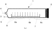
- Figure 1 shows schematically an example of a diffusion oven 1 with door 2 at one end and terminal wall 3 with one or more gas inlets 4 and one or more gas outlets 5 at the opposite end.
- a processing boat 7 on which several silicon wafers 8 are arranged.
- the section of the inner volume 6 of the diffusion oven 1 that is located near the terminal wall 3 is typically referred to as gas zone 6a
- the section that is located near the door 2 is typically referred to as load zone 6c
- the section between gas zone 6a and load zone 6c is typically referred to as center zone 6b.
- the heating means for the diffusion oven 1 which are not shown in figure 1 , are arranged in such a way that temperatures and/or the heating power can be adjusted individually for gas zone 6a, center zone 6b and load zone 6c. If used for the method according to the invention, the diffusion oven 1 may be operating under normal pressure conditions or under reduced pressure relative to ambient pressure.
- the gas flow through gas inlets 4 is controlled by valves (not shown), which can usually be set remotely by a controller (not shown) to provide a given flow rate of the respective gas type flowing into the inner volume 6 of the diffusion oven 1.
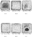
- Figures 2a-c and 3a-c show the sheet resistance of wafers from the gas zone 6a (c.f. Fig. 2a,3a ), the center zone 6b (c.f.
- Fig. 2b,3b and the load zone 6c (c.f. Fig. 2c,3c ) of the diffusion oven 1 obtained by a state of the art doping process performed with a first set of fixed gas flow parameters and a second set of fixed gas flow parameters, respectively. More specifically, in each case a fully loaded boat with 200 silicon wafers 8 was exposed for 26 minutes to a temperature over the heating zones that was adjusted to 970°C +/- 3°C to a particular gas flow.
- flow ratio 1 and flow ratio 2 of these examples the same flow rates of doping gas and reactive gas are used and only the amount of reactive gas is varied. It should be pointed out that in order to realize the invention, it is also possible to vary flow rates of carrier gas and/or doping gas.
- the most relevant parameter for influencing the zone in which good homogeneity is achieved is the ratio of doping gas to reactive gas that is used. However, the inventors have found that the preferred way of influencing this ratio is variation of the reactive gas flow.
- the above-presented flow rate of the doping gas is actually the rate at which BBr 3 is carried into the oven as a result of bubbling 70 cm 3 /min N 2 gas through a bottle containing liquid BBr 3 . Changing this flow condition renders control of the BBr 3 pickup inaccurate, especially if this change is repeated.
- the exact process parameters that have to be used to achieve this depend e.g. on the type of the diffusion oven 1, the number of silicon wafers 8 to be processed in the oven 1 and the exact parameters of the desired doping process and therefore should preferably be established individually before starting standardized production runs. For standard processes, this may be done by the oven manufacturer for a given oven type, but alternatively it is possible to determine the parameters most suited for a given purpose by trial runs with systematic variation of gas flow parameters and analyzing the thus obtained results on silicon wafers 8 from different zones 6a,6b,6c of the diffusion oven 1 individually.
- the next parameter to be varied is the flow of reactive gas.
- the flow of reactive gas As a general trend, from the above mentioned starting point lowering values of reactive gas tend to lead to improved homogeneity in the load zone 6c whereas increasing values of reactive gas tend to lead to improved homogeneity in the gas zone 6a.
- Further degrees of freedom comprise an adaption of the carrier gas flow rate and the temperature setting of the zones 6a,6b,6c of the diffusion oven 1.
- Figure 4a illustrates an example diagram showing the gas flow regulation as a function of time as proposed by this invention.
- the flow rate of doping gas and carrier gas are kept constant and the flow rate of the reactive gas is changed between a high flow value f2, creating improved conditions for homogeneity in the gas zone 6a, and a low flow value f1, creating improved conditions for homogeneity in the load zone 6c.
- the cycling between these conditions is repeated four times over the deposition process, so that there are four periods of time with high reactive gas flow f2 and four periods of time with low reactive gas flow f1.
- the effect is not specific for a given doping gas, reaction gas and/or carrier gas.
- all doping gases that can be used for Boron doping, especially BBr 3 and BCl 3 may be used together with the respective reaction gases, especially O 2 , H 2 or H 2 O steam, and carrier gases, especially N 2 or Ar.
- it can be adapted to the respective time scale of a given doping process as long as enough settling time for the gas flow after a change of gas flow settings can be provided.
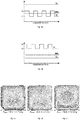
- figures 5 a-c show the results obtained using the process conditions described above for flow ratio 1 and flow ratio 2, respectively in connection with a gas flow regulation as shown in the diagram of figure 4a .
- a gas flow regulation as shown in the diagram of figure 4a .
- Fig. 4b is diagram showing an example for a variation of gas flow over deposition time in accordance with the variant of this invention in which the flow rate of the carrier gas is changed during deposition time, which also increases homogeneity of the achieved doping characteristics over the length of the oven.
- This variant is especially effective in doping procedures in which the oven is operated at reduced pressure relative to the ambient pressure.
- timing of the carrier gas flow variations relative to the reactive gas flow variations may be preferable as a function of the respective doping process and diffusion oven parameters.
- the inventors tentatively assume that under reduced pressure conditions a reduction of the phase shift may lead to improved results.
- Fig. 7 is a diagram showing in its upper half flow rates of N 2 (solid line, upper half) and O 2 when used for drive in (dashed line, upper half) and in its lower half flow rates of O 2 when used as reactive gas (solid line, lower half) and BBr 3 doping gas (dashed line, lower half).
- the presented flow rate of the doping gas is actually the rate at which BBr 3 is carried into the oven as a result of bubbling 70 cm 3 /min N 2 gas through a bottle containing liquid BBr 3 .
- the oven which is typically already pre-heated, e.g to a temperature of 830°C, is loaded with the wafers. As shown in Figure 7 , this occurs under high N 2 (i.e. carrier gas) flow.
- N 2 i.e. carrier gas
- the conditions in the oven After loading, it is preferable to allow the conditions in the oven to settle for a stabilization time after loading to allow different furnace zones to reach a predetermined temperature difference. During this stabilization time, the carrier gas flow is reduced and reaction gas flow, e.g. O 2 flow, is started. However, this is not yet part of the deposition phase, because no doping gas is flowing.
- reaction gas flow e.g. O 2 flow
- the deposition phase is started by switching on the doping gas flow only after the stabilization time is over. Typically, at the time the deposition phase is started the temperature is also being ramped up, e.g. to 970°C with a temperature increase of 8°C/minute.
- the deposition phase is ended after a defined time by switching off the BBr 3 flow.
- cool-down to unload temperature e.g. 850°C with a ramp of 4°C/minute
- the drive-in phase is started under O 2 flow with switched off N 2 carrier gas in order to achieve oxidation before O 2 flos is stopped and N 2 flow is switched back on. Note that in this situation the O 2 is no longer used as reaction gas to provide the dopant chemically, as doping gas is no longer provided.
Landscapes
- Chemical Vapour Deposition (AREA)
- Crystals, And After-Treatments Of Crystals (AREA)
Claims (12)
- Verfahren zum Dotieren von Silizium-Wafern (8) unter Verwendung eines Diffusions-Ofens (1), wobei besagter Diffusions-Ofen (1) eine Tür (2) zum Laden und Entladen der Silizium-Wafer (8), einen Innenraum (6), Gaseinlässe (4) für ein Reaktionsgas, ein Dotierungsgas und ein Trägergas und Mittel zur Modifikation der Flussrate des besagten Reaktionsgases, des besagten Dotierungsgases und des besagten Trägergases in den Innenraum (6) des Diffusions-Ofens (1) hat, wobei das besagte Verfahren die Schritte- Laden von Silizium-Wafern (8) in den Diffusions-Ofen (1),- Beheizen des Diffusions-Ofens (1) gemäß einem vorgegebenen Temperaturprofil zumindest während einer Depositionszeit,- gleichzeitiges Einströmen lassen von Reaktionsgas, Dotierungsgas und Trägergas in den Innenraum (6) und- Entladen der Silizium-Wafer (8) aus dem Diffusions-Ofen (1)
aufweist,
dadurch gekennzeichnet, dass während der Depositions-Zeit, in der Reaktionsgas, Dotierungsgas und Trägergas gleichzeitig in den Innenraum (6) des Diffusions-Ofens (1) einströmen, das Verhältnis zwischen der Flussrate des Reaktionsgases und der Flussrate des Dotierungsgases wenigstens einmal von einem ersten Verhältnis zu einem zweiten Verhältnis geändert wird und/oder die Flussrate des Trägergases wenigstens einmal von einer ersten Flussrate zu einer zweiten Flussrate geändert wird. - Verfahren zum Dotieren von Silizium-Wafern nach Anspruch 1,
dadurch gekennzeichnet, dass das Verhältnis der Flussrate des Reaktionsgases und der Flussrate des Dotierungsgases wenigstens einmal von einem ersten Verhältnis zu einem zweiten Verhältnis geändert wird und dass das erste Verhältnis oder das zweite Verhältnis so gewählt ist, dass es zu homogen dotierten Silizium-Wafern (8) in der Nachbarschaft der Gaseinlässe führt, wenn es über die Depositionszeit hinweg angewendet wird und das zweite Verhältnis oder das erste Verhältnis so gewählt ist, dass es zu homogen dotierten Wafern in dem Bereich des Innenraums (6), der den Gaseinlässen gegenüber liegt, führt, wenn es über die Depositionszeit hinweg angewendet wird. - Verfahren zum Dotieren von Silizium-Wafern nach Anspruch 2,
dadurch gekennzeichnet, dass das Verfahren ferner den Schritt des Bestimmens des ersten Verhältnisses, das zu homogen dotierten Wafern in der Nachbarschaft der Gaseinlässe führt, wenn es über die Depositionszeit hinweg angewendet wird und das Bestimmen des zweiten Verhältnisses, das zu homogen dotierten Wafern in dem Bereich des Innenraums (6), der den Gaseinlässen gegenüber liegt, führt, wenn es über die Depositionszeit hinweg angewendet wird, umfasst. - Verfahren zum Dotieren von Silizium-Wafern nach Anspruch 2 oder 3,
dadurch gekennzeichnet, dass das Verfahren ferner wenigstens einmal während der Depositionszeit das Verändern des Verhältnisses zwischen der Flussrate des Reaktionsgases und der Flussrate des Dotierungsgases zu wenigstens einem dritten Verhältnis umfasst. - Verfahren zum Dotieren von Silizium-Wafern nach Anspruch 4,
dadurch gekennzeichnet, dass das dritte Verhältnis so gewählt ist, dass es zu homogen dotierten Wafern im Zentralbereich (6b) des Innenraums des Diffusions-Ofens 1 führt, wenn es über die Depositionszeit hinweg angewendet wird. - Verfahren zum Dotieren von Silizium-Wafern nach Anspruch 1,
dadurch gekennzeichnet, dass die Flussrate des Trägergases wenigstens einmal von einer ersten Flussrate zu einer zweiten Flussrate geändert wird und dass die erste Flussrate oder die zweite Flussrate so gewählt ist, dass sie zu homogen dotierten Silizium-Wafern (8) in der Nachbarschaft der Gaseinlässe führt, wenn sie über die Depositionszeit hinweg angewendet wird und die zweite Flussrate oder die erste Flussrate so gewählt ist, dass sie zu homogen dotierten Wafern in dem Bereich des Innenraums (6), der den Gaseinlässen gegenüber liegt, führt, wenn sie über die Depositionszeit hinweg angewendet wird. - Verfahren zum Dotieren von Silizium-Wafern nach Anspruch 6,
dadurch gekennzeichnet, dass das Verfahren ferner den Schritt des Bestimmens der ersten Flussrate, die zu homogen dotierten Wafern in der Nachbarschaft der Gaseinlässe führt, wenn sie über die Depositionszeit hinweg angewendet wird und des Bestimmens der zweiten Flussrate, die zu homogen dotierten Wafern in dem Bereich des Innenraums (6), der den Gaseinlässen gegenüber liegt, führt, wenn sie über die Depositionszeit hinweg angewendet wird, umfasst. - Verfahren zum Dotieren von Silizium-Wafern nach Anspruch 6 oder 7,
dadurch gekennzeichnet, dass das Verfahren ferner wenigstens einmal während der Depositionszeit das Verändern der Flussrate des Trägergases und der Flussrate des Dotierungsgases zu wenigstens einer dritten Flussrate umfasst. - Verfahren zum Dotieren von Silizium-Wafern nach Anspruch 8,
dadurch gekennzeichnet, dass die dritte Flussrate so gewählt ist, dass sie zu homogen dotierten Wafern im Zentralbereich (6b) des Innenraums des Diffusions-Ofens 1 führt, wenn es über die Depositionszeit hinweg angewendet wird. - Verfahren zum Dotieren von Silizium-Wafern nach einem der vorstehenden Ansprüche,
dadurch gekennzeichnet, dass das Wechseln zwischen den Verhältnissen und/oder das Wechseln zwischen den Flussraten mehrmals während der Depositionszeit, insbesondere zyklisch oder anti-zyklisch erfolgt. - Verfahren zum Dotieren von Silizium-Wafern nach einem der vorstehenden Ansprüche,
dadurch gekennzeichnet, dass das Verhältnis zwischen der Flussrate des Reaktionsgases und der Flussrate des Dotierungsgases wenigstens einmal von einem ersten Verhältnis zu einem zweiten Verhältnis geändert wird und die Flussrate des Trägergases wenigstens einmal von einer ersten Flussrate zu einer zweiten Flussrate geändert wird und dass das Ändern der Flussrate des Trägergases phasenverschoben zum Ändern zwischen den Verhältnissen erfolgt. - Verfahren zum Dotieren von Silizium-Wafern nach einem der vorstehenden Ansprüche,
dadurch gekennzeichnet, dass das Umschalten zwischen den Verhältnissen und/oder das Umschalten zwischen den Flussraten des Trägergases weniger oft als einmal pro Minute erfolgt.
Priority Applications (4)
| Application Number | Priority Date | Filing Date | Title |
|---|---|---|---|
| EP15171263.5A EP3104397B1 (de) | 2015-06-09 | 2015-06-09 | Verfahren zur dotierung von siliciumwafern |
| PCT/EP2016/062676 WO2016198338A1 (en) | 2015-06-09 | 2016-06-03 | Method for doping silicon wafers |
| CN201680033418.XA CN107690693B (zh) | 2015-06-09 | 2016-06-03 | 掺杂硅晶片的方法 |
| HK18106754.3A HK1247440B (zh) | 2015-06-09 | 2016-06-03 | 掺杂矽晶片的方法 |
Applications Claiming Priority (1)
| Application Number | Priority Date | Filing Date | Title |
|---|---|---|---|
| EP15171263.5A EP3104397B1 (de) | 2015-06-09 | 2015-06-09 | Verfahren zur dotierung von siliciumwafern |
Publications (2)
| Publication Number | Publication Date |
|---|---|
| EP3104397A1 EP3104397A1 (de) | 2016-12-14 |
| EP3104397B1 true EP3104397B1 (de) | 2017-10-11 |
Family
ID=53404367
Family Applications (1)
| Application Number | Title | Priority Date | Filing Date |
|---|---|---|---|
| EP15171263.5A Active EP3104397B1 (de) | 2015-06-09 | 2015-06-09 | Verfahren zur dotierung von siliciumwafern |
Country Status (3)
| Country | Link |
|---|---|
| EP (1) | EP3104397B1 (de) |
| CN (1) | CN107690693B (de) |
| WO (1) | WO2016198338A1 (de) |
Families Citing this family (4)
| Publication number | Priority date | Publication date | Assignee | Title |
|---|---|---|---|---|
| CN108110088B (zh) * | 2017-12-21 | 2020-11-10 | 苏州阿特斯阳光电力科技有限公司 | 太阳能电池的低压扩散工艺及利用其制备得到的太阳能电池 |
| DE102020133390A1 (de) | 2020-12-14 | 2022-06-15 | Hanwha Q Cells Gmbh | Verfahren zur Herstellung eines Bor-Emitters auf einem Silizium-Wafer |
| CN115458612B (zh) * | 2022-10-27 | 2024-08-20 | 通威太阳能(眉山)有限公司 | 一种太阳电池及其制备方法 |
| US20240258118A1 (en) * | 2023-01-27 | 2024-08-01 | Destination 2D Inc. | Large-area wafer-scale cmos-compatible 2d-material intercalation doping tools, processes, and methods, including doping of synthesized graphene |
Family Cites Families (10)
| Publication number | Priority date | Publication date | Assignee | Title |
|---|---|---|---|---|
| EP1142004B1 (de) | 1998-12-17 | 2004-10-13 | Vishay Semiconductor Itzehoe GmbH | Verfahren zur bor-dotierung von wafern unter einsatz eines vertikalofensystems |
| EP2077587A4 (de) * | 2006-09-27 | 2016-10-26 | Kyocera Corp | Solarzellenanordnung und verfahren zu ihrer herstellung |
| FR2944138B1 (fr) | 2009-04-06 | 2012-12-07 | Semco Engineering Sa | Procede de dopage au bore de plaquettes de silicium |
| CN101707226B (zh) * | 2009-07-29 | 2012-05-09 | 湖南红太阳新能源科技有限公司 | 晶体硅太阳能电池的扩散工艺 |
| DE102012207764B4 (de) * | 2012-05-09 | 2022-08-11 | International Solar Energy Research Center Konstanz E.V. | Verfahren zur Bor-Dotierung von Silizium-Wafern |
| DE102012018746A1 (de) * | 2012-09-21 | 2014-03-27 | Fraunhofer-Gesellschaft zur Förderung der angewandten Forschung e.V. | Verfahren zur Dotierung von Halbleitersubstraten |
| CN102916086A (zh) * | 2012-10-31 | 2013-02-06 | 湖南红太阳光电科技有限公司 | 一种低方阻晶体硅电池的扩散工艺 |
| DE102012025429A1 (de) * | 2012-12-21 | 2014-06-26 | Fraunhofer-Gesellschaft zur Förderung der angewandten Forschung e.V. | Verfahren zur Dotierung von Halbleitersubstraten sowie dotiertes Halbleitersubstrat |
| CN103646999A (zh) * | 2013-12-18 | 2014-03-19 | 上饶光电高科技有限公司 | 一种改善太阳能电池片均匀性的磷扩散方法 |
| CN103681976A (zh) * | 2013-12-27 | 2014-03-26 | 百力达太阳能股份有限公司 | 一种高效低成本太阳电池扩散工艺 |
-
2015
- 2015-06-09 EP EP15171263.5A patent/EP3104397B1/de active Active
-
2016
- 2016-06-03 CN CN201680033418.XA patent/CN107690693B/zh active Active
- 2016-06-03 WO PCT/EP2016/062676 patent/WO2016198338A1/en not_active Ceased
Non-Patent Citations (1)
| Title |
|---|
| None * |
Also Published As
| Publication number | Publication date |
|---|---|
| WO2016198338A1 (en) | 2016-12-15 |
| HK1247440A1 (zh) | 2018-09-21 |
| CN107690693B (zh) | 2022-01-07 |
| EP3104397A1 (de) | 2016-12-14 |
| CN107690693A (zh) | 2018-02-13 |
Similar Documents
| Publication | Publication Date | Title |
|---|---|---|
| KR101149383B1 (ko) | 반도체 장치의 제조 방법 및 기판 처리 장치 | |
| EP3104397B1 (de) | Verfahren zur dotierung von siliciumwafern | |
| JP4512098B2 (ja) | 半導体装置の製造方法及び基板処理装置 | |
| JP3945519B2 (ja) | 被処理体の熱処理装置、熱処理方法及び記憶媒体 | |
| JP6017396B2 (ja) | 薄膜形成方法および薄膜形成装置 | |
| EP1388891B1 (de) | System zur wärmebehandlung von halbleiter | |
| JP5476637B2 (ja) | ゲッターによる多結晶グループiiiの金属窒化物および作製方法 | |
| KR101897191B1 (ko) | 실리콘 웨이퍼 붕소 도핑 방법 | |
| CN101150050A (zh) | 半导体处理用氧化装置和方法 | |
| WO2008118531A2 (en) | Oxide-containing film formed from silicon | |
| KR102139435B1 (ko) | 에피택셜 실리콘 웨이퍼의 제조 방법 | |
| KR102470917B1 (ko) | 성막 방법 및 성막 장치 | |
| KR20050026708A (ko) | 반도체 웨이퍼의 열처리 장치 및 열처리 방법 | |
| KR20170113275A (ko) | 붕소 도프 실리콘 게르마늄막의 형성 방법 및 형성 장치, 및 기억 매체 | |
| AU2002358050B2 (en) | Baking oven for photovoltaic devices | |
| KR101225477B1 (ko) | 반도체 장치의 제조 방법 및 기판 처리 장치 | |
| WO2002084711A1 (en) | Heating system and method for heating an atmospheric reactor | |
| HK1247440B (zh) | 掺杂矽晶片的方法 | |
| JP6450851B2 (ja) | エピタキシャルウェーハの成長のためのリアクターの再稼動準備方法 | |
| KR102848609B1 (ko) | 성막 방법 및 성막 장치 | |
| CN111886679B (zh) | 半导体装置的制造方法、基板处理装置以及记录介质 | |
| US9478423B2 (en) | Method of vapor-diffusing impurities | |
| TWI588904B (zh) | Heat treatment method | |
| CN116024547A (zh) | 半导体处理设备中的颗粒消除方法 | |
| KR20230146453A (ko) | 성막 방법 및 처리 장치 |
Legal Events
| Date | Code | Title | Description |
|---|---|---|---|
| PUAI | Public reference made under article 153(3) epc to a published international application that has entered the european phase |
Free format text: ORIGINAL CODE: 0009012 |
|
| AK | Designated contracting states |
Kind code of ref document: A1 Designated state(s): AL AT BE BG CH CY CZ DE DK EE ES FI FR GB GR HR HU IE IS IT LI LT LU LV MC MK MT NL NO PL PT RO RS SE SI SK SM TR |
|
| AX | Request for extension of the european patent |
Extension state: BA ME |
|
| 17P | Request for examination filed |
Effective date: 20170320 |
|
| RBV | Designated contracting states (corrected) |
Designated state(s): AL AT BE BG CH CY CZ DE DK EE ES FI FR GB GR HR HU IE IS IT LI LT LU LV MC MK MT NL NO PL PT RO RS SE SI SK SM TR |
|
| GRAP | Despatch of communication of intention to grant a patent |
Free format text: ORIGINAL CODE: EPIDOSNIGR1 |
|
| INTG | Intention to grant announced |
Effective date: 20170519 |
|
| GRAS | Grant fee paid |
Free format text: ORIGINAL CODE: EPIDOSNIGR3 |
|
| GRAA | (expected) grant |
Free format text: ORIGINAL CODE: 0009210 |
|
| AK | Designated contracting states |
Kind code of ref document: B1 Designated state(s): AL AT BE BG CH CY CZ DE DK EE ES FI FR GB GR HR HU IE IS IT LI LT LU LV MC MK MT NL NO PL PT RO RS SE SI SK SM TR |
|
| REG | Reference to a national code |
Ref country code: GB Ref legal event code: FG4D |
|
| REG | Reference to a national code |
Ref country code: CH Ref legal event code: EP |
|
| REG | Reference to a national code |
Ref country code: IE Ref legal event code: FG4D |
|
| REG | Reference to a national code |
Ref country code: AT Ref legal event code: REF Ref document number: 936726 Country of ref document: AT Kind code of ref document: T Effective date: 20171115 |
|
| REG | Reference to a national code |
Ref country code: DE Ref legal event code: R096 Ref document number: 602015005243 Country of ref document: DE |
|
| REG | Reference to a national code |
Ref country code: NL Ref legal event code: FP |
|
| REG | Reference to a national code |
Ref country code: LT Ref legal event code: MG4D |
|
| REG | Reference to a national code |
Ref country code: AT Ref legal event code: MK05 Ref document number: 936726 Country of ref document: AT Kind code of ref document: T Effective date: 20171011 |
|
| PG25 | Lapsed in a contracting state [announced via postgrant information from national office to epo] |
Ref country code: ES Free format text: LAPSE BECAUSE OF FAILURE TO SUBMIT A TRANSLATION OF THE DESCRIPTION OR TO PAY THE FEE WITHIN THE PRESCRIBED TIME-LIMIT Effective date: 20171011 Ref country code: SE Free format text: LAPSE BECAUSE OF FAILURE TO SUBMIT A TRANSLATION OF THE DESCRIPTION OR TO PAY THE FEE WITHIN THE PRESCRIBED TIME-LIMIT Effective date: 20171011 Ref country code: FI Free format text: LAPSE BECAUSE OF FAILURE TO SUBMIT A TRANSLATION OF THE DESCRIPTION OR TO PAY THE FEE WITHIN THE PRESCRIBED TIME-LIMIT Effective date: 20171011 Ref country code: NO Free format text: LAPSE BECAUSE OF FAILURE TO SUBMIT A TRANSLATION OF THE DESCRIPTION OR TO PAY THE FEE WITHIN THE PRESCRIBED TIME-LIMIT Effective date: 20180111 Ref country code: LT Free format text: LAPSE BECAUSE OF FAILURE TO SUBMIT A TRANSLATION OF THE DESCRIPTION OR TO PAY THE FEE WITHIN THE PRESCRIBED TIME-LIMIT Effective date: 20171011 |
|
| PG25 | Lapsed in a contracting state [announced via postgrant information from national office to epo] |
Ref country code: LV Free format text: LAPSE BECAUSE OF FAILURE TO SUBMIT A TRANSLATION OF THE DESCRIPTION OR TO PAY THE FEE WITHIN THE PRESCRIBED TIME-LIMIT Effective date: 20171011 Ref country code: AT Free format text: LAPSE BECAUSE OF FAILURE TO SUBMIT A TRANSLATION OF THE DESCRIPTION OR TO PAY THE FEE WITHIN THE PRESCRIBED TIME-LIMIT Effective date: 20171011 Ref country code: HR Free format text: LAPSE BECAUSE OF FAILURE TO SUBMIT A TRANSLATION OF THE DESCRIPTION OR TO PAY THE FEE WITHIN THE PRESCRIBED TIME-LIMIT Effective date: 20171011 Ref country code: RS Free format text: LAPSE BECAUSE OF FAILURE TO SUBMIT A TRANSLATION OF THE DESCRIPTION OR TO PAY THE FEE WITHIN THE PRESCRIBED TIME-LIMIT Effective date: 20171011 Ref country code: GR Free format text: LAPSE BECAUSE OF FAILURE TO SUBMIT A TRANSLATION OF THE DESCRIPTION OR TO PAY THE FEE WITHIN THE PRESCRIBED TIME-LIMIT Effective date: 20180112 Ref country code: BG Free format text: LAPSE BECAUSE OF FAILURE TO SUBMIT A TRANSLATION OF THE DESCRIPTION OR TO PAY THE FEE WITHIN THE PRESCRIBED TIME-LIMIT Effective date: 20180111 Ref country code: IS Free format text: LAPSE BECAUSE OF FAILURE TO SUBMIT A TRANSLATION OF THE DESCRIPTION OR TO PAY THE FEE WITHIN THE PRESCRIBED TIME-LIMIT Effective date: 20180211 |
|
| REG | Reference to a national code |
Ref country code: FR Ref legal event code: PLFP Year of fee payment: 4 |
|
| REG | Reference to a national code |
Ref country code: DE Ref legal event code: R097 Ref document number: 602015005243 Country of ref document: DE |
|
| PG25 | Lapsed in a contracting state [announced via postgrant information from national office to epo] |
Ref country code: DK Free format text: LAPSE BECAUSE OF FAILURE TO SUBMIT A TRANSLATION OF THE DESCRIPTION OR TO PAY THE FEE WITHIN THE PRESCRIBED TIME-LIMIT Effective date: 20171011 Ref country code: EE Free format text: LAPSE BECAUSE OF FAILURE TO SUBMIT A TRANSLATION OF THE DESCRIPTION OR TO PAY THE FEE WITHIN THE PRESCRIBED TIME-LIMIT Effective date: 20171011 Ref country code: CZ Free format text: LAPSE BECAUSE OF FAILURE TO SUBMIT A TRANSLATION OF THE DESCRIPTION OR TO PAY THE FEE WITHIN THE PRESCRIBED TIME-LIMIT Effective date: 20171011 Ref country code: SK Free format text: LAPSE BECAUSE OF FAILURE TO SUBMIT A TRANSLATION OF THE DESCRIPTION OR TO PAY THE FEE WITHIN THE PRESCRIBED TIME-LIMIT Effective date: 20171011 |
|
| PLBE | No opposition filed within time limit |
Free format text: ORIGINAL CODE: 0009261 |
|
| STAA | Information on the status of an ep patent application or granted ep patent |
Free format text: STATUS: NO OPPOSITION FILED WITHIN TIME LIMIT |
|
| PG25 | Lapsed in a contracting state [announced via postgrant information from national office to epo] |
Ref country code: PL Free format text: LAPSE BECAUSE OF FAILURE TO SUBMIT A TRANSLATION OF THE DESCRIPTION OR TO PAY THE FEE WITHIN THE PRESCRIBED TIME-LIMIT Effective date: 20171011 Ref country code: IT Free format text: LAPSE BECAUSE OF FAILURE TO SUBMIT A TRANSLATION OF THE DESCRIPTION OR TO PAY THE FEE WITHIN THE PRESCRIBED TIME-LIMIT Effective date: 20171011 Ref country code: SM Free format text: LAPSE BECAUSE OF FAILURE TO SUBMIT A TRANSLATION OF THE DESCRIPTION OR TO PAY THE FEE WITHIN THE PRESCRIBED TIME-LIMIT Effective date: 20171011 |
|
| 26N | No opposition filed |
Effective date: 20180712 |
|
| PG25 | Lapsed in a contracting state [announced via postgrant information from national office to epo] |
Ref country code: SI Free format text: LAPSE BECAUSE OF FAILURE TO SUBMIT A TRANSLATION OF THE DESCRIPTION OR TO PAY THE FEE WITHIN THE PRESCRIBED TIME-LIMIT Effective date: 20171011 |
|
| REG | Reference to a national code |
Ref country code: CH Ref legal event code: PL |
|
| REG | Reference to a national code |
Ref country code: BE Ref legal event code: MM Effective date: 20180630 |
|
| REG | Reference to a national code |
Ref country code: IE Ref legal event code: MM4A |
|
| PG25 | Lapsed in a contracting state [announced via postgrant information from national office to epo] |
Ref country code: LU Free format text: LAPSE BECAUSE OF NON-PAYMENT OF DUE FEES Effective date: 20180609 Ref country code: MC Free format text: LAPSE BECAUSE OF FAILURE TO SUBMIT A TRANSLATION OF THE DESCRIPTION OR TO PAY THE FEE WITHIN THE PRESCRIBED TIME-LIMIT Effective date: 20171011 |
|
| PG25 | Lapsed in a contracting state [announced via postgrant information from national office to epo] |
Ref country code: IE Free format text: LAPSE BECAUSE OF NON-PAYMENT OF DUE FEES Effective date: 20180609 Ref country code: CH Free format text: LAPSE BECAUSE OF NON-PAYMENT OF DUE FEES Effective date: 20180630 Ref country code: LI Free format text: LAPSE BECAUSE OF NON-PAYMENT OF DUE FEES Effective date: 20180630 |
|
| PG25 | Lapsed in a contracting state [announced via postgrant information from national office to epo] |
Ref country code: BE Free format text: LAPSE BECAUSE OF NON-PAYMENT OF DUE FEES Effective date: 20180630 |
|
| PG25 | Lapsed in a contracting state [announced via postgrant information from national office to epo] |
Ref country code: MT Free format text: LAPSE BECAUSE OF NON-PAYMENT OF DUE FEES Effective date: 20180609 |
|
| PG25 | Lapsed in a contracting state [announced via postgrant information from national office to epo] |
Ref country code: PT Free format text: LAPSE BECAUSE OF FAILURE TO SUBMIT A TRANSLATION OF THE DESCRIPTION OR TO PAY THE FEE WITHIN THE PRESCRIBED TIME-LIMIT Effective date: 20171011 |
|
| PG25 | Lapsed in a contracting state [announced via postgrant information from national office to epo] |
Ref country code: MK Free format text: LAPSE BECAUSE OF NON-PAYMENT OF DUE FEES Effective date: 20171011 Ref country code: CY Free format text: LAPSE BECAUSE OF FAILURE TO SUBMIT A TRANSLATION OF THE DESCRIPTION OR TO PAY THE FEE WITHIN THE PRESCRIBED TIME-LIMIT Effective date: 20171011 Ref country code: RO Free format text: LAPSE BECAUSE OF FAILURE TO SUBMIT A TRANSLATION OF THE DESCRIPTION OR TO PAY THE FEE WITHIN THE PRESCRIBED TIME-LIMIT Effective date: 20171011 Ref country code: HU Free format text: LAPSE BECAUSE OF FAILURE TO SUBMIT A TRANSLATION OF THE DESCRIPTION OR TO PAY THE FEE WITHIN THE PRESCRIBED TIME-LIMIT; INVALID AB INITIO Effective date: 20150609 |
|
| PG25 | Lapsed in a contracting state [announced via postgrant information from national office to epo] |
Ref country code: AL Free format text: LAPSE BECAUSE OF FAILURE TO SUBMIT A TRANSLATION OF THE DESCRIPTION OR TO PAY THE FEE WITHIN THE PRESCRIBED TIME-LIMIT Effective date: 20171011 |
|
| REG | Reference to a national code |
Ref country code: DE Ref legal event code: R081 Ref document number: 602015005243 Country of ref document: DE Owner name: "INTERNATIONAL SOLAR ENERGY RESEARCH CENTER KO, DE Free format text: FORMER OWNER: INTERNATIONAL SOLAR ENERGY RESEARCH CENTER KONSTANZ E.V., 78467 KONSTANZ, DE |
|
| P01 | Opt-out of the competence of the unified patent court (upc) registered |
Free format text: CASE NUMBER: UPC_APP_412861/2023 Effective date: 20230505 |
|
| PGFP | Annual fee paid to national office [announced via postgrant information from national office to epo] |
Ref country code: GB Payment date: 20250620 Year of fee payment: 11 |
|
| PGFP | Annual fee paid to national office [announced via postgrant information from national office to epo] |
Ref country code: NL Payment date: 20250618 Year of fee payment: 11 |
|
| PGFP | Annual fee paid to national office [announced via postgrant information from national office to epo] |
Ref country code: FR Payment date: 20250626 Year of fee payment: 11 |
|
| PGFP | Annual fee paid to national office [announced via postgrant information from national office to epo] |
Ref country code: TR Payment date: 20250530 Year of fee payment: 11 |
|
| PGFP | Annual fee paid to national office [announced via postgrant information from national office to epo] |
Ref country code: DE Payment date: 20250728 Year of fee payment: 11 |
|
| REG | Reference to a national code |
Ref country code: DE Ref legal event code: R079 Ref document number: 602015005243 Country of ref document: DE Free format text: PREVIOUS MAIN CLASS: H01L0021225000 Ipc: H10P0032140000 |