EP3103893A1 - Vacuum vapor deposition method - Google Patents
Vacuum vapor deposition method Download PDFInfo
- Publication number
- EP3103893A1 EP3103893A1 EP16177892.3A EP16177892A EP3103893A1 EP 3103893 A1 EP3103893 A1 EP 3103893A1 EP 16177892 A EP16177892 A EP 16177892A EP 3103893 A1 EP3103893 A1 EP 3103893A1
- Authority
- EP
- European Patent Office
- Prior art keywords
- vaporization
- substrate
- containers
- release holes
- equal
- Prior art date
- Legal status (The legal status is an assumption and is not a legal conclusion. Google has not performed a legal analysis and makes no representation as to the accuracy of the status listed.)
- Granted
Links
- 238000007740 vapor deposition Methods 0.000 title claims abstract description 40
- 238000000034 method Methods 0.000 title claims abstract description 27
- 238000009834 vaporization Methods 0.000 claims abstract description 329
- 230000008016 vaporization Effects 0.000 claims abstract description 329
- 239000000758 substrate Substances 0.000 claims abstract description 116
- 239000000463 material Substances 0.000 claims abstract description 115
- 238000000151 deposition Methods 0.000 claims abstract description 96
- 230000008021 deposition Effects 0.000 claims abstract description 90
- 238000010438 heat treatment Methods 0.000 claims description 20
- 238000001771 vacuum deposition Methods 0.000 claims 2
- 239000010408 film Substances 0.000 description 45
- 239000010409 thin film Substances 0.000 description 36
- 238000002156 mixing Methods 0.000 description 28
- 238000010586 diagram Methods 0.000 description 15
- 238000009826 distribution Methods 0.000 description 15
- 230000015572 biosynthetic process Effects 0.000 description 13
- 230000007246 mechanism Effects 0.000 description 12
- 239000011368 organic material Substances 0.000 description 7
- 230000005855 radiation Effects 0.000 description 5
- 238000001816 cooling Methods 0.000 description 4
- 230000003449 preventive effect Effects 0.000 description 4
- 238000004364 calculation method Methods 0.000 description 3
- 238000004519 manufacturing process Methods 0.000 description 3
- 229910052751 metal Inorganic materials 0.000 description 3
- 239000002184 metal Substances 0.000 description 3
- 230000008859 change Effects 0.000 description 2
- 239000000498 cooling water Substances 0.000 description 2
- 239000002019 doping agent Substances 0.000 description 2
- 230000006872 improvement Effects 0.000 description 2
- 238000005259 measurement Methods 0.000 description 2
- 239000007769 metal material Substances 0.000 description 2
- 230000008569 process Effects 0.000 description 2
- 239000011364 vaporized material Substances 0.000 description 2
- 238000004804 winding Methods 0.000 description 2
- 229910052782 aluminium Inorganic materials 0.000 description 1
- XAGFODPZIPBFFR-UHFFFAOYSA-N aluminium Chemical compound [Al] XAGFODPZIPBFFR-UHFFFAOYSA-N 0.000 description 1
- 239000013078 crystal Substances 0.000 description 1
- 238000005137 deposition process Methods 0.000 description 1
- 238000009792 diffusion process Methods 0.000 description 1
- 238000007599 discharging Methods 0.000 description 1
- 230000000694 effects Effects 0.000 description 1
- 230000008020 evaporation Effects 0.000 description 1
- 238000001704 evaporation Methods 0.000 description 1
- 230000004907 flux Effects 0.000 description 1
- 238000005286 illumination Methods 0.000 description 1
- 238000009434 installation Methods 0.000 description 1
- 239000011810 insulating material Substances 0.000 description 1
- 239000004973 liquid crystal related substance Substances 0.000 description 1
- 230000004048 modification Effects 0.000 description 1
- 238000012986 modification Methods 0.000 description 1
- 239000011295 pitch Substances 0.000 description 1
- 230000000630 rising effect Effects 0.000 description 1
- 238000004088 simulation Methods 0.000 description 1
- 239000000344 soap Substances 0.000 description 1
- 238000000859 sublimation Methods 0.000 description 1
- 230000008022 sublimation Effects 0.000 description 1
Images


Classifications
-
- C—CHEMISTRY; METALLURGY
- C23—COATING METALLIC MATERIAL; COATING MATERIAL WITH METALLIC MATERIAL; CHEMICAL SURFACE TREATMENT; DIFFUSION TREATMENT OF METALLIC MATERIAL; COATING BY VACUUM EVAPORATION, BY SPUTTERING, BY ION IMPLANTATION OR BY CHEMICAL VAPOUR DEPOSITION, IN GENERAL; INHIBITING CORROSION OF METALLIC MATERIAL OR INCRUSTATION IN GENERAL
- C23C—COATING METALLIC MATERIAL; COATING MATERIAL WITH METALLIC MATERIAL; SURFACE TREATMENT OF METALLIC MATERIAL BY DIFFUSION INTO THE SURFACE, BY CHEMICAL CONVERSION OR SUBSTITUTION; COATING BY VACUUM EVAPORATION, BY SPUTTERING, BY ION IMPLANTATION OR BY CHEMICAL VAPOUR DEPOSITION, IN GENERAL
- C23C14/00—Coating by vacuum evaporation, by sputtering or by ion implantation of the coating forming material
- C23C14/22—Coating by vacuum evaporation, by sputtering or by ion implantation of the coating forming material characterised by the process of coating
- C23C14/24—Vacuum evaporation
-
- C—CHEMISTRY; METALLURGY
- C23—COATING METALLIC MATERIAL; COATING MATERIAL WITH METALLIC MATERIAL; CHEMICAL SURFACE TREATMENT; DIFFUSION TREATMENT OF METALLIC MATERIAL; COATING BY VACUUM EVAPORATION, BY SPUTTERING, BY ION IMPLANTATION OR BY CHEMICAL VAPOUR DEPOSITION, IN GENERAL; INHIBITING CORROSION OF METALLIC MATERIAL OR INCRUSTATION IN GENERAL
- C23C—COATING METALLIC MATERIAL; COATING MATERIAL WITH METALLIC MATERIAL; SURFACE TREATMENT OF METALLIC MATERIAL BY DIFFUSION INTO THE SURFACE, BY CHEMICAL CONVERSION OR SUBSTITUTION; COATING BY VACUUM EVAPORATION, BY SPUTTERING, BY ION IMPLANTATION OR BY CHEMICAL VAPOUR DEPOSITION, IN GENERAL
- C23C14/00—Coating by vacuum evaporation, by sputtering or by ion implantation of the coating forming material
- C23C14/22—Coating by vacuum evaporation, by sputtering or by ion implantation of the coating forming material characterised by the process of coating
- C23C14/24—Vacuum evaporation
- C23C14/243—Crucibles for source material
-
- C—CHEMISTRY; METALLURGY
- C23—COATING METALLIC MATERIAL; COATING MATERIAL WITH METALLIC MATERIAL; CHEMICAL SURFACE TREATMENT; DIFFUSION TREATMENT OF METALLIC MATERIAL; COATING BY VACUUM EVAPORATION, BY SPUTTERING, BY ION IMPLANTATION OR BY CHEMICAL VAPOUR DEPOSITION, IN GENERAL; INHIBITING CORROSION OF METALLIC MATERIAL OR INCRUSTATION IN GENERAL
- C23C—COATING METALLIC MATERIAL; COATING MATERIAL WITH METALLIC MATERIAL; SURFACE TREATMENT OF METALLIC MATERIAL BY DIFFUSION INTO THE SURFACE, BY CHEMICAL CONVERSION OR SUBSTITUTION; COATING BY VACUUM EVAPORATION, BY SPUTTERING, BY ION IMPLANTATION OR BY CHEMICAL VAPOUR DEPOSITION, IN GENERAL
- C23C14/00—Coating by vacuum evaporation, by sputtering or by ion implantation of the coating forming material
- C23C14/06—Coating by vacuum evaporation, by sputtering or by ion implantation of the coating forming material characterised by the coating material
- C23C14/12—Organic material
-
- H—ELECTRICITY
- H10—SEMICONDUCTOR DEVICES; ELECTRIC SOLID-STATE DEVICES NOT OTHERWISE PROVIDED FOR
- H10K—ORGANIC ELECTRIC SOLID-STATE DEVICES
- H10K71/00—Manufacture or treatment specially adapted for the organic devices covered by this subclass
- H10K71/10—Deposition of organic active material
- H10K71/16—Deposition of organic active material using physical vapour deposition [PVD], e.g. vacuum deposition or sputtering
- H10K71/164—Deposition of organic active material using physical vapour deposition [PVD], e.g. vacuum deposition or sputtering using vacuum deposition
-
- C—CHEMISTRY; METALLURGY
- C23—COATING METALLIC MATERIAL; COATING MATERIAL WITH METALLIC MATERIAL; CHEMICAL SURFACE TREATMENT; DIFFUSION TREATMENT OF METALLIC MATERIAL; COATING BY VACUUM EVAPORATION, BY SPUTTERING, BY ION IMPLANTATION OR BY CHEMICAL VAPOUR DEPOSITION, IN GENERAL; INHIBITING CORROSION OF METALLIC MATERIAL OR INCRUSTATION IN GENERAL
- C23C—COATING METALLIC MATERIAL; COATING MATERIAL WITH METALLIC MATERIAL; SURFACE TREATMENT OF METALLIC MATERIAL BY DIFFUSION INTO THE SURFACE, BY CHEMICAL CONVERSION OR SUBSTITUTION; COATING BY VACUUM EVAPORATION, BY SPUTTERING, BY ION IMPLANTATION OR BY CHEMICAL VAPOUR DEPOSITION, IN GENERAL
- C23C14/00—Coating by vacuum evaporation, by sputtering or by ion implantation of the coating forming material
- C23C14/22—Coating by vacuum evaporation, by sputtering or by ion implantation of the coating forming material characterised by the process of coating
- C23C14/54—Controlling or regulating the coating process
- C23C14/542—Controlling the film thickness or evaporation rate
- C23C14/543—Controlling the film thickness or evaporation rate using measurement on the vapor source
Definitions
- the present invention relates to a vacuum vapor method apparatus which forms a thin film by depositing multiple vaporization materials simultaneously on a deposition target such as a substrate.
- a vacuum vapor deposition apparatus is an apparatus for forming a thin film as follows. First, a deposition target and a vaporization container containing a vaporization material are placed inside a vacuum chamber in the apparatus. Then, while the inside of the vacuum chamber is depressurized, the vaporization container is heated to melt and vaporize the vaporization material through evaporation or sublimation. The vaporized material is then deposited on a surface of the deposition target to thereby form a thin film.
- the vacuum vapor deposition apparatus employs methods such as an external heating method using an external heater to heat the vaporization container containing the vaporization material.
- vacuum vapor deposition apparatuses have been used not only to form metal thin films and oxide thin films using metal materials, but also to form organic thin films by depositing organic materials, as well as to form small molecular organic thin films by simultaneously depositing multiple organic materials.
- vacuum vapor deposition apparatuses are used to form organic electroluminescent elements (hereinafter, referred to as organic EL elements) for flat panel displays.
- the vacuum vapor deposition apparatus is also capable of forming a thin film by simultaneously depositing multiple vaporization materials on a substrate or the like (simultaneous deposition).
- a host material and a luminescent material are used as the vaporization materials. These materials are simultaneously deposited to form the luminescent layer.
- the mixing ratio of a host material and a luminescent material is an important factor that influences the properties of the luminescent layer.
- a conventional vacuum vapor deposition apparatus ⁇ Patent Literature 1> includes a vaporization source which allows a vaporization material to be vaporized through linearly-arranged multiple openings. The vaporized material is then deposited on a large substrate by moving the vaporization source and the substrate relative to each other, whereby a thin film having a relatively uniform film thickness is formed.
- a vaporization source which allows a vaporization material to be vaporized through linearly-arranged multiple openings.
- the vaporized material is then deposited on a large substrate by moving the vaporization source and the substrate relative to each other, whereby a thin film having a relatively uniform film thickness is formed.
- These demands have been satisfied by reducing the distance between a vaporization source and a substrate.
- the present invention has been made in view of the above circumstances, and has an object to provide a vacuum vapor deposition method capable of forming a homogeneous thin film having a constant mixing ratio of multiple vaporization materials in the film thickness direction, when mixing and depositing the vaporization materials using multiple linear-shaped vaporization sources.
- a vacuum vapor deposition method for solving the above problem, a plurality of vaporization containers each containing a vaporization material and having a plurality of release holes arranged linearly are placed in parallel with arrangement directions of the plurality of release holes.
- the vaporization containers are heated to evaporate or sublimate the respective vaporization materials, and vapors of the respective materials are released through the plurality of release holes.
- the vaporization materials are mixed together and deposited on an entire surface of a substrate by relatively moving the substrate and the vaporization containers in a direction perpendicular to the arrangement directions of the plurality of release holes.
- the apparatus is characterized in that equal-thickness surfaces (or equal film thickness surfaces) are calculated for the vaporization containers, respectively, each of the equal-thickness surfaces indicating where a deposition amount of the vapor (or film thickness) of the vaporization material released from the release holes in the corresponding vaporization container is the same per unit time.
- the vaporization containers are placed in such a manner that contact points of the respective equal-thickness surfaces all coincide with each other on the surface of the substrate, each of the contact points indicating where the corresponding equal-thickness surfaces come in contact with the surface of the substrate.
- a vacuum vapor deposition apparatus for solving the above problem according to a second invention provides the vacuum vapor deposition method described above having the following features.
- the vaporization containers include nozzles projecting from the vaporization containers and where the release holes are provided to penetrate through the nozzles
- the vaporization containers are placed to stand vertically and the nozzles are tilted in such a manner that the contact points of the respective equal-thickness surfaces all coincide with each other on the surface of the substrate.
- each of the contact points indicates where the corresponding equal-thickness surfaces come in contact with the surface of the substrate.
- the vaporization containers can include therein a current plate having a plurality of passage holes through which the corresponding vapor passes.
- conductance by the passage holes is made proportional to conductance by the release holes.
- the vaporization containers are placed in such a manner that contact points of the equal-thickness surfaces, at which they come in contact with the surface of the substrate, would coincide with each other on the surface of the substrate.
- each equal-thickness surface indicates where the deposition amount of the vapor of the corresponding vaporization material is the same per unit time.
- the vaporization containers each include therein the current plate having the multiple passage holes, and as conductance per unit length in the longitudinal directions of the vaporization containers, conductance by the passage holes is made proportional to conductance by the release holes.
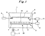
- Fig. 1 is a schematic configuration diagram showing the configuration of a vacuum vapor deposition apparatus of a first example.
- Fig. 1 shows a cross section taken along a plane perpendicular to the transport direction of a substrate in the vacuum vapor deposition apparatus.
- the vacuum vapor deposition apparatus of the first example is installed as a part (vacuum vapor deposition apparatus section) of an inline system for forming organic EL elements.
- the vacuum vapor deposition apparatus of the first example will be described below by taking formation of an organic EL element as an example; however, the vacuum vapor deposition apparatus of the first example is not limited to this, and is applicable to formation of a metal thin film of a metal material, an insulating thin film of an insulating material, and the like.
- the vacuum vapor deposition apparatus of the first example is also applicable to deposition using only one vaporization material as well as to deposition using multiple vaporization materials (multi-source simultaneous deposition; also called co-deposition in a case of two vaporization materials).
- the inline system includes multiple processing apparatuses (e.g., a vacuum vapor deposition apparatus, and the like).
- the whole system is configured by a vacuum chamber through which multiple substrates are transported continuously, each substrate being subjected to successive processes for formation of organic EL elements (e.g., formation of luminescent layers as organic thin films, formation of electrodes as metal thin films, and the like).
- organic EL elements e.g., formation of luminescent layers as organic thin films, formation of electrodes as metal thin films, and the like.
- These processes require structures for carrying in the substrates from the atmosphere side to the vacuum chamber and for carrying out the substrates from the vacuum chamber, such as a charging chamber and a discharging chamber. These structures may be obtained by known techniques, and thus illustration thereof is omitted here.
- a vacuum chamber 1 is connected to a vacuum pump 3 via a valve 2 as shown in Fig. 1 , allowing the inside of the vacuum chamber 1 to be evacuated to a high vacuum state.
- a substrate 4 on which to deposit an organic thin film is positioned on the center of an unillustrated tray. With rotation of transport rollers 6 driven by a drive source 5, the substrate 4 is transported together with the tray from the front side toward the further side of Fig. 1 .
- vaporization sources 20 to be described later are fixed at certain positions and the substrate 4 is caused to move; in contrast, the substrate 4 may be fixed at a certain position and the vaporization sources 20 may be caused to move.
- each vaporization source 20 is formed as a linear-shaped vaporization source elongated in the horizontal direction (hereinafter, referred to as a broad width direction of the substrate 4) perpendicular to the transport direction of the substrate 4, and has a length equal to or slightly greater than the length of the substrate 4 in the board width direction.
- a broad width direction of the substrate perpendicular to the transport direction of the substrate 4
- multiple vaporization sources 20 are arranged in parallel with the board width direction of the substrate 4 as shown in Figs. 5 and 6 to be described later.
- each vaporization container 8 provided is a vaporization rate detector 10 (e.g., crystal monitor head or the like) to detect the vaporization rate of the corresponding vaporization material 7 vaporized from the vaporization container 8.
- This vaporization rate detector 10 is connected to a vaporization rate controller 11.
- the vaporization rate controller 11 controls the control output to a heating power source 12 on the basis of the vaporization rate detected by the vaporization rate detector 10 so that the vaporization rate would remain at a predetermined value.
- the heating power source 12 feeds the heater 9 with the power controlled on the basis of the control output so that the vaporization rate would remain constant.
- the control described above refers to control of temperature at the time of deposition.
- each individual vaporization source 20 is provided with the above-mentioned heating mechanism and the control mechanisms.
- each vaporization container 8 is heated using the vaporization rate detector 10, the vaporization rate controller 11, the heating power source 12, and the heater 9 as described above, the vaporization material 7 contained in the vaporization container 8 is evaporated or sublimated. The vapor of the vaporization material 7 is then released in accordance with a constant vaporization rate through multiple release holes 13 to be described later.
- the board width direction of the substrate 4 is the same as the direction in which the multiple release holes 13 are arranged.
- the substrate 4 and each vaporization source 20 are caused to relatively move in the direction perpendicular to the board width direction and the direction in which the release holes 13 are arranged. Hence, the vaporization materials 7 vaporized from the respective vaporization sources 20 are mixed together and deposited on the entire surface of the substrate 4.
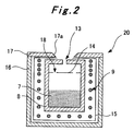
- Fig. 2 is a cross-sectional view of the vaporization source of the first example, taken along a plane perpendicular to the longitudinal direction of the linear vaporization source.
- each vaporization source has the same structure.
- the vaporization container 8 placed inside the vaporization source 20 is formed to be elongated in the board width direction of the substrate 4, and has a length equal to or slightly greater than the length of the substrate 4 in the board width direction.
- the multiple release holes 13 are provided in an upper surface (surface on the substrate 4 side) of the vaporization container 8.
- a current plate 14 having multiple passage holes 18 is placed between the release holes 13 and the vaporization material 7 inside the vaporization container 8.
- the positions of the release holes 13 and the passage holes 18 in the longitudinal direction are arranged in such a manner that the film thickness distribution of a thin film formed by deposition of the vaporization material 7 would be uniform in the board width direction of the substrate 4.
- the heater 9 is not placed above the vaporization container 8. Accordingly, in order to compensate temperature decrease in the release holes 13, the heater 9 is disposed densely on the release holes 13 side and the lower heater 9 is disposed sparsely on a lower side (on the vaporization material 7 side). Such disposition prevents temperature decrease in the release holes 13 and thus avoids clogging of the release holes 13 by the vaporization material 7.
- the heater 9 and the heating power source 12 will be further described later using Figs. 3A and 3B .
- a radiation preventive plate 15 is placed around the entire surface of the outer periphery of the heater 9 except a part immediately above the release holes 13. This radiation preventive plate 15 functions to preserve and equalize the heat of the vaporization container 8. Moreover, an outer periphery of the radiation preventive plate 15 is covered by a water-cooling jacket 16 and a heat insulating plate 17.
- the water-cooling jacket 16 has therein a passage (unillustrated) through which cooling water flows and is cooled by the cooling water.
- the heat insulating plate 17 has opening portions 17a at positions corresponding to the arrangement positions of the release holes 13 and is in contact with an upper opening portion of the water-cooling jacket 16.
- the water-cooling jacket 16 and the heat insulating plate 17 functions to prevent heat radiation to the vacuum chamber 1 and the substrate 4.
- Fig. 3A is a diagram for explaining the configuration of the heating mechanism and the control mechanism of the first example.
- Patent Literature 1 is a method by which multiple temperature control means are provided separately in the longitudinal direction and vaporization rate control is performed for each separate region.
- the heating mechanism to heat the vaporization container 8 is formed by one heating power source 12 and one heater 9, and the control mechanism therefore is formed by one vaporization rate detector 10 and one vaporization rate controller 11 as shown in Fig. 3A .
- the heating mechanism and the control mechanism serves as a single system.
- the heater 9 is formed of one hot wire wound in spirals around an outer surface of the vaporization container 8.
- the heater 9 is disposed in such a manner that its pitches would be denser on the release holes 13 side than on the vaporization container 7 side, by winding the heater 9 densely around an upper portion (the release holes 13 side) of the vaporization container 8 and sparsely around a lower portion (the vaporization material 7 side) thereof.
- Such structure allows single system heat control. Accordingly, it is possible to control the vaporization rate easily and stably over a long period of time, allowing formation of a thin film having a uniform film thickness and thus formation of an element having stable properties.
- the heater 9 since the heater 9 is wound around the outer surface of the vaporization container 8 multiple times, one heater may not provide a sufficient output if a required overall length exceeds a usable heater length. In such case, multiple heaters may be used. When multiple heaters are to be used, the heaters are similarly wound around the outer surface of the vaporization container 8. For example, as shown in Fig. 3B , two heaters may be used which are a heater 9a wound densely on an upper portion side and a heater 9b wound sparsely on a lower portion side. In this case, the heaters 9a and 9b are connected to each other in parallel or series so that power is fed thereto using one heating power source 12. This structure also allows single system heat control. Accordingly, it is possible to control the vaporization rate easily and stably over a long period of time, allowing formation of a thin film having a uniform film thickness and thus formation of an element having stable properties.
- both heaters 9a and 9b can be disposed in the longitudinal direction of the vaporization container 8. Accordingly, even in the case of using multiple heaters, an influence in heating by the difference between the heaters 9a and 9b does not appear in the longitudinal direction of the vaporization container 8. Hence, the temperature distribution of the vaporization container 8 in its longitudinal direction can be made uniform.
- Fig. 4A is a cross-sectional view of the vaporization container 8 in its longitudinal direction.
- Fig. 4B is a top view of the vaporization container 8.
- Fig. 4C is a top view of the current plate 14.
- the amount of vapor vaporized from the vaporization material 7 itself will be called a "vaporization amount”
- the amount of vapor other than that such as the amount of vapor in the release holes 13 and in the passage holes 18 will be called a "vapor amount” to make a clear distinction therebetween.
- the multiple release holes 13 are formed in an upper surface (surface on the substrate 4 side) of the vaporization container 8 linearly in the longitudinal direction of the vaporization container 8. All the release holes 13 have a circular shape with the same diameter (with the same area). The release holes 13 are arranged such that the intervals therebetween would be denser toward both end portions from the center of the vaporization container 8 in its longitudinal direction. In this way, conductance by the release hole 13 becomes larger toward both end portions of the vaporization container 8. Assuming that the intervals between the release holes 13 from each end side to the center are W 11 , W 12 , W 13 , and W 14 in Fig. 4B for example, the intervals W 13 and W 14 near the center are equivalent, and the intervals W 11 , W 12 , W 13 , and W 14 have a relationship of W 14 ⁇ W 13 > W 12 > W 11 from the center to each end side.
- the vaporization source 20 is a linear-shaped vaporization source.
- the linear vaporization source 20 may be assumed as what is obtained by arranging many point vaporization sources. For this reason, the thickness distribution, in the board width direction of the substrate 4, of a film formed by the linear vaporization source 20 can be calculated based on geometric superposition of amounts of vapor released from the many point vaporization sources. Using this fact, a vapor amount necessary for each assumptive point vaporization source on the vaporization source 20 is calculated so that the film thickness distribution in the board width direction of the substrate 4 would be uniform.
- conductance on the upper surface of the vaporization container 8 is calculated per unit length.
- conductance of each of the release holes 13 can be calculated based on the diameter and length of the release hole 13 and the average speed of vaporized molecules (see Gorou Tominaga, Hiroo Kumagai, "Shinkuu no Butsuri to Ouyou,” Shokabo Publishing Co., Ltd, 1970 , or the like for example) . Accordingly, the arrangement intervals between the release holes 13 in the longitudinal direction of the vaporization container 8 are calculated.
- Calculation of the arrangement intervals of the release holes 13 in the longitudinal direction of the vaporization container 8 indicates as follows.
- the arrangement intervals between the release holes 13 on both end sides need to be denser than the arrangement intervals between the release holes 13 on the center side (i.e., conductance per unit length needs to be larger on both end sides than on the center side), in order to make the film thickness distribution uniform in the board width direction of the substrate 4.
- the intervals have the relationship of W 14 ⁇ W 13 > W 12 > W 11 as mentioned above. It should be noted that such arrangement intervals of the release holes 13 are set under the assumption that the vapor amount of the vaporization material 7 immediately below the release holes 13 is uniform.
- a variation in temperature of the vaporization container 8 and/or a change in state of the vaporization material 7 itself may largely vary a vaporization state, which may possibly make the vaporization amount ununiform in the longitudinal direction of the vaporization container 8.
- the vaporization material 7 is an organic material
- state of the material may be changed significantly by a temperature variation.
- the vaporization amount becomes ununiform in the longitudinal direction, and, additionally, the vaporization material 7 may be left unevenly along with consumption of the vaporization material 7. This, as a result, makes the vaporization amount even more ununiform in the longitudinal direction.
- the current plate 14 having the passage holes 18 through which the vapor of the vaporization material 7 passes is provided inside the vaporization container 8 so that the vapor amounts of the vaporization material 7 immediately below the release holes 13 are made uniform.
- this configuration it is possible to handle ununiform vaporization amounts of the vaporization material 7 in the longitudinal direction.
- the structure of the current plate 14 will be described with reference to Fig. 4C .
- the current plate 14 is placed between the release holes 13 and the vaporization material 7 inside the vaporization container 8 so as to separate the release holes 13 side and the vaporization material 7 side.
- the multiple passage holes 18 are provided to penetrate through the current plate 14 and formed to be aligned in two straight lines extending in the longitudinal direction of the current plate 14. All the passage holes 18 have a circular shape with the same diameter (with the same area). The passage holes 18 are arranged such that the intervals therebetween would be denser toward both end portions from the center of the current plate 14 in its longitudinal direction. In this way, conductance by the passage holes 18 is made proportional to conductance by the release holes 13.
- the intervals between the passage holes 18 from each end side to the center are W 21 , W 22 , W 23 , W 24 , and W 25 in Fig. 4C for example, the intervals W 23 , W 24 , and W 25 near the center are mutually equivalent, and the intervals W 21 , W 22 , W 23 , W 24 , and W 25 have a relationship of W 25 ⁇ W 24 ⁇ W 23 > W 22 > W 21 from the center to each end side.
- the passage holes 18 are arranged such that the release holes 13 and the passage holes 18 are not aligned colinearly when viewed from the surface of the vaporization material 7, for the following reason.
- the vaporization material 7 may be a material that is easy to bump (splash), such as an organic material. When such material bumps, the above arrangement prevents the vapor generated by the bumping from directly passing the passage holes 18 and the release holes 13 to directly adhere to the substrate 4. Since the arrangement prevents vapor generated by bumping from directly adhering to the substrate 4, it is possible to significantly improve a product quality.
- the amounts of vapor passing through the release holes 13 on both end sides of the vaporization container 8 are smaller than the estimated amounts. This hinders improvement of the film thickness distribution in the board width direction of the substrate 4.
- the vaporization amounts of the vaporization material 7 become ununiform in the longitudinal direction. As a result, the film thickness distribution in the board width direction of the substrate 4 is deteriorated.
- the arrangement intervals between the passage holes 18 are calculated in basically the same way as the arrangement intervals between the release holes 13. For example, a vapor amount necessary for each assumptive point vaporization source on the current plate 14 is calculated so that the vapor amounts immediately below the release holes 13 would be uniform. Based on the calculated vapor amounts, conductance on the upper surface of the current plate 14 is calculated per unit length. Then, based on the calculated conductance per unit length and conductance of each of the release holes 18, the arrangement intervals between the passage holes 18 in the longitudinal direction of the current plate 14 are calculated. Calculation of the arrangement intervals between the passage holes 18 in the longitudinal direction of the current plate 14 indicates as follows.
- the arrangement intervals between the passage holes 18 on both end sides need to be denser than the arrangement intervals between the passage holes 18 on the center side (i.e., conductance per unit length needs to be larger on both end sides than on the center side), in order to make uniform the vapor amounts immediately below the release holes 13.
- the intervals have the relationship of W 25 ⁇ W 24 ⁇ W 23 > W 22 > W 21 as mentioned above. Accordingly, the arrangement intervals between the release holes 13 and the arrangement intervals between the passage holes 18 come to have the same arrangement tendency. Thereby, as conductance per unit length in the longitudinal direction, conductance by the passage holes 18 is made proportional to conductance by the release holes 13.
- the arrangement intervals of the release holes 13 having the same diameter are changed to alter conductance per unit length in the vaporization container 8.
- the arrangement intervals between the release holes 13 may be set at a fixed length, and, instead, the sizes of the release holes 13 may be changed to alter conductance per unit length.
- the arrangement intervals of the passage holes 18 having the same diameter are changed to alter conductance per unit length for the current plate 14.
- the arrangement intervals between the passage holes 18 may be set at a fixed length, and, instead, the sizes of the passage holes 18 may be changed to alter conductance per unit length.
- release holes 13 and the passage holes 18 each have a circular shape in Figs. 4B and 4C described above, but may have a square shape, an elliptic shape, a rectangular shape, or the like. Furthermore, one release hole 13 is associated with two passage holes 18 but may be associated with one or otherwise many (3 or more) passage holes 18.
- the current plate 14 is provided inside the vaporization container 8, and the release holes 13 in the vaporization container 8 and the passage holes 18 in the current plate 14 are arranged to have the positional relationship mentioned above. Accordingly, the vapor amounts immediately below the release holes 13 can be made uniform, which in turn increases the amount of vapor flow on each end side compared to that on the center side. This suppresses a decrease in film thickness at both end portions of the substrate 4 and thus makes uniform the film thickness distribution in the board width direction of the substrate 4. Consequently, a thin film having a desired uniform film thickness distribution can be obtained.
- Fig. 6A is a diagram for explaining how two vaporization sources are placed in general
- Fig. 5B is a graph showing the profile of the deposition amounts at certain positions in the transport direction regarding the placement.
- Fig. 6A is a diagram for explaining how two vaporizations sources are placed in the first example
- Fig. 6B is a graph showing the profile of the deposition amounts at certain positions in the transport direction regarding the placement.
- Fig. 7 is a diagram for explaining how three vaporization sources are placed in the first example. Note that description will be given while showing only the substrate and the vaporization containers inside the vaporization sources in Figs. 5A to 7 for simple illustration.
- vaporization containers 8a and 8b are placed to tilt in such a manner that normal lines La and Lb from the centers of release holes 13a and 13b of the vaporization containers 8a and 8b, respectively, coincides with one another on a deposition surface of the substrate 4, as shown in Fig. 5A .
- calculation of equal-thickness surfaces 19a and 19b for the vaporization containers 8a and 8b indicates as follows, each of the equal-thickness surfaces 19a and 19b being where the deposition amount of the vapor of vaporization material released from corresponding one of release holes 13a and 13b is the same per unit time.
- the equal-thickness surfaces 19a and 19b intersect with each other at a position where the deposition surface of the substrate 4 intersects with the normal lines La and Lb (also intersecting with a center line C showing the apparatus center in Fig. 5A ).
- the equal-thickness surfaces 19a and 19b are desirably spherical or ellipsoidal (see Tatsuo Asamaki, Hakumaku Sakusei no Kiso, The Nikkan Kogyo Shimbun, Ltd., 2005 , or the like for example).
- the equal-thickness surfaces 19a and 19b are depicted as ellipsoidal.
- the equal-thickness surfaces 19a and 19b are similar to how soap bubbles inflate while becoming thinner.
- the equal-thickness surfaces 19a and 19b indicate positions where adhesion of equal film thickness takes place.
- the equal-thickness surfaces are depicted as having the same shape and size. This means for example that the equal-thickness surface 19a represents a film thickness of 100 nm, the equal-thickness surface 19b represents a film thickness of 1 nm, and thus a film having a mixing ratio of 100:1 is formed.
- the equal-thickness surfaces 19a and 19b expand from the vaporization containers 8a and 8b, respectively, and come in contact with the substrate 4 before intersecting with each other on the substrate 4.
- the positions where the equal-thickness surfaces 19a and 19b first come in contact with the substrate 4 are positions where the thicknesses of the films deposited from the vaporization containers 8a and 8b become the largest.
- Fig. 5B is a graph showing deposition amounts (corresponding to film thicknesses) within such a range that the distance between the substrate 4 and the vaporization containers 8a and 8b is 1, and the distance in the transport direction is 4.
- the deposition amounts from the vaporization containers 8a and 8b are different from each other, but their largest deposition amounts are illustrated as being equal for the sake of comparison.
- the mixing ratio in the formed film is the same as a whole, the mixing ratio deviates at any position in the transport direction, and the amounts of the deviation are large.
- the substrate 4 is subjected to simultaneous deposition while moving in the transport direction T.
- the profile shown in Fig. 5B corresponds to the mixing ratio in the film thickness direction of the thin film formed by the simultaneous deposition, and the deviated mixing ratio indicates that the mixing ratio of the deposited vaporization materials vary in the film thickness direction of the deposited thin film. For this reason, the film is hardly a homogeneous thin film.
- the vaporization containers 8a and 8b are placed to tilt in such a manner that contact points of the equal-thickness surfaces 19a and 19b, at which they come in contact with the deposition surface of the substrate 4, would coincide with each other on the deposition surface of the substrate 4, as shown in Fig. 6A .
- a host material and a luminescent material as vaporization materials need to be mixed and deposited.
- the equal-thickness surface 19a and the equal-thickness surface 19b are calculated in accordance with the mixing ratio of the host material and the luminescent material.
- the equal-thickness surface 19a indicates where the deposition amount of the vapor of the host material released from the release holes 13a is the same per unit time
- the equal-thickness surface 19b indicates where the deposition amount of the vapor of the luminescent material released from the release holes 13b is the same per unit time.
- the vaporization containers 8a and 8b are placed to tilt in such a manner that contact points of the obtained equal-thickness surfaces 19a and 19b, at which they come in contact with the deposition surface of the substrate 4, would coincide with each other on the deposition surface of the substrate 4.
- the equal-thickness surfaces 19a and 19b described above can be calculated through simulations of vapor flux distributions using parameters such as the temperatures, positions, and inclinations of the vaporization containers 8a and 8b in accordance with the types of vaporization materials.
- an equal-thickness surface from one release hole 13 is a spherical or ellipsoidal matter (whose cross section is circular or elliptic) having the release hole 13 as its origin.
- the equal-thickness surfaces 19a and 19b may be regarded as continuously-connected spherical or ellipsoidal matters obtained by partially superposing the spherical or ellipsoidal matters on one another in the arrangement directions of the respective multiple release holes 13a and 13b. That is, the equal-thickness surfaces 19a and 19b may be regarded as elongated matters having circular or elliptic cross sections.
- the contact points of the equal-thickness surfaces 19a and 19b, at which they come in contact with the deposition surface of the substrate 4 coincides with each other on the deposition surface of the substrate 4 at any position in the arrangement directions of the multiple release holes 13a and 13b
- the contact points of the equal-thickness surfaces 19a and 19b, at which they come in contact with the deposition surface of the substrate 4 is regarded as substantially coinciding with each other on the deposition surface of the substrate 4 at all the positions in the arrangement directions of the multiple release holes 13a and 13b.
- the sizes of the equal-thickness surfaces 19a and 19b remain the same regardless of the types of vaporization materials or film thicknesses but differ from each other depending on the distances between the vaporization sources and the substrate.
- films can be formed with a desired mixing ratio.
- Measurement of the deposition amounts in the height direction of the substrate 4 at each position in the transport direction T shows the following.
- the deposition amounts with the vapors of the respective vaporization materials both take their largest values at a position where the deposition surface of the substrate 4 intersect with the center line C. With these positions as the peaks, the deposition amounts each decrease symmetrically.
- the mixing ratio at the center line C position is a desired mixing ratio.
- the mixing ratios at the other positions deviate by a quite small margin. Nonetheless, the deviated amounts are significantly smaller than those in Fig. 5B .
- the substrate 4 is subjected to simultaneous deposition while moving in the transport direction T.
- the first example makes it possible to keep the mixing ratio in the film thickness direction substantially constant and thus to form a homogeneous thin film, thereby enabling manufacturing of an organic EL element or the like with a higher quality.
- a position in the transport direction where the deposition amount of the vaporization material vaporized from the vaporization container 8a reaches largest in the height direction of the substrate 4 coincides, on the deposition surface of the substrate 4, with a position in the transport direction where the deposition amount of the vaporization material vaporized from the vaporization container 8b reaches largest in the height direction of the substrate 4.
- the normal lines La, Lb, and Lc from the centers of the release holes 13a, 13b, and 13c of the vaporization containers 8a, 8b, and 8c, respectively, should not coincide with one another on the deposition surface of the substrate 4. Instead, equal-thickness surfaces 19a, 19b, and 19c are calculated for the vaporization containers 8a, 8b, and 8c, respectively.
- each of the equal-thickness surfaces 19a, 19b, and 19c indicates where the deposition amount of the vapor of the vaporization material released from corresponding one of the release holes 13a, 13b, and 13c is the same per unit time. Then, the vaporization containers 8a, 8b, and 8c are placed to tilt in such a manner that contact points of the equal-thickness surfaces 19a, 19b, and 19c, at which they come in contact with the deposition surface of the substrate 4, would all coincide with one another on the deposition surface of the substrate 4.
- the mixing ratio in the film thickness direction is kept substantially constant and thus a homogeneous thin film is formed.
- an organic EL element with a higher quality can be manufactured.
- the materials in the vaporization containers 8a and 8b on both sides should be host materials whereas the material in the vaporization container 8c in the middle should be a luminescent material as dopant.
- a vaporization source shown in Fig. 8 is also applicable to the present invention. In that case, the other configurations may be the same as those described in the first example, and thus only the vaporization source is illustrated here.
- Fig. 8 is a cross-sectional view taken along a plane perpendicular to the longitudinal direction of the linear-shaped vaporization source.
- a vaporization source 20' of a second example has approximately the same structure as that of the vaporization source 20 shown in Fig. 2 .
- nozzles 21 projecting up to an upper surface of the heat insulating plate 17 are provided to an upper surface (surface on the substrate 4 side) of a vaporization container 8', and the release holes 13 are provided to penetrate through the nozzles 21.
- the position of the upper plane of each release hole 13 in its height direction is made as high as the position of the upper surface of the heat insulating plate 17 in its height direction. This eliminates a possibility of the vapor of the vaporization material 7 adhering to the heat insulating plate 17.
- opening portions 17b in the heat insulating plate 17 do not need to be tapered and, instead, are formed to penetrate vertically through the heat insulating plate 17.
- the other configurations are the same as those of the vaporization source 20 shown in Fig. 2 , and thus the same components in Fig. 8 are denoted by the same reference signs and description thereof will be omitted.
- Fig. 9 is a diagram for explaining how two vaporization sources are placed in the second example.
- Fig. 10 is a diagram for explaining how three vaporization sources are placed in the second example. Note that description will be given also in Figs. 9 and 10 while showing only the substrate and the vaporization containers inside the vaporization sources for simple illustration.
- equal-thickness surfaces 24a and 24b are calculated for the vaporization containers 8a' and 8b', respectively.
- each of the equal-thickness surfaces 24a and 24b indicates where the deposition amount of the vapor of the vaporization material released from corresponding one of nozzles 21a and 21b is the same per unit time. Then, as shown in Fig.
- vaporization containers 8a' and 8b' are placed to stand vertically and also nozzles 21a and 21b thereof are tilted in such a manner that contact points of equal-thickness surfaces 24a and 24b, at which they come in contact with the deposition surface of the substrate 4, would coincide with each other on the deposition surface of the substrate 4.
- the equal-thickness surfaces 24a and 24b are calculated for the vaporization containers 8a' and 8b', respectively. Under the same conditions, the sizes of the equal-thickness surfaces 24a and 24b remain the same regardless of the types of vaporization materials or film thicknesses but differ from each other depending on the distances between the vaporization sources and the substrate. Thus, by using the vaporization rate detectors 10 and the vaporization rate controllers 11 to detect and control the deposition amounts (vaporization rates) from the vaporization containers 8a' and 8b', respectively, films can be formed with a desired mixing. Nonetheless, it is desirable that the sizes of the equal-thickness surfaces 24a and 24b of the vaporization materials be approximately equal to each other. In this way, it is possible to place the vaporization containers 8a' and 8b' symmetrically with respect to the center line C, and also to obtain deposition amount profile as shown in Fig. 6B described above.
- the normal lines La, Lb, and Lc from the centers of the nozzles 21a, 21b, and 21c of the vaporization containers 8a', 8b', and 8c', respectively, should not coincide with one another on the deposition surface of the substrate 4. Instead, the equal-thickness surfaces 24a, 24b, and 24c are calculated for the vaporization containers 8a', 8b', and 8c', respectively.
- each of the equal-thickness surfaces 24a, 24b, and 24c indicates where the deposition amount of the vapor of the vaporization material released from corresponding one of the nozzles 21a, 21b, and 21c is the same per unit time. Then, as shown in Fig. 10 , the vaporization containers 8a', 8b', and 8c' are placed to stand vertically and also the nozzles 21a, 21b, and 21c thereof are tilted in such a manner that contact points of the equal-thickness surface 24a, 24b, and 24c, at which they come in contact with the deposition surface of the substrate 4, would all coincide with one another on the deposition surface of the substrate 4.
- the mixing ratio in the film thickness direction is kept substantially constant and thus a homogeneous thin film is formed.
- an organic EL element with a higher quality can be manufactured.
- the materials in the vaporization containers 8a' and 8b'on both sides should be host materials whereas the material in the vaporization container 8c in the middle should be a luminescent material as dopant.
- the vaporization containers 8a', 8b', and 8c' do not need to be placed in a tilted manner, and thus can be installed easily.
- a vacuum vapor deposition apparatus is suitable particularly for a case where the deposition target is a large substrate, and also suitable for a case where the vaporization materials are organic materials.
Landscapes
- Chemical & Material Sciences (AREA)
- Engineering & Computer Science (AREA)
- Chemical Kinetics & Catalysis (AREA)
- Materials Engineering (AREA)
- Mechanical Engineering (AREA)
- Metallurgy (AREA)
- Organic Chemistry (AREA)
- Manufacturing & Machinery (AREA)
- Physical Vapour Deposition (AREA)
- Electroluminescent Light Sources (AREA)
Abstract
Description
- The present invention relates to a vacuum vapor method apparatus which forms a thin film by depositing multiple vaporization materials simultaneously on a deposition target such as a substrate.
- A vacuum vapor deposition apparatus is an apparatus for forming a thin film as follows. First, a deposition target and a vaporization container containing a vaporization material are placed inside a vacuum chamber in the apparatus. Then, while the inside of the vacuum chamber is depressurized, the vaporization container is heated to melt and vaporize the vaporization material through evaporation or sublimation. The vaporized material is then deposited on a surface of the deposition target to thereby form a thin film. As a method of heating the vaporization container, the vacuum vapor deposition apparatus employs methods such as an external heating method using an external heater to heat the vaporization container containing the vaporization material. In recent years, vacuum vapor deposition apparatuses have been used not only to form metal thin films and oxide thin films using metal materials, but also to form organic thin films by depositing organic materials, as well as to form small molecular organic thin films by simultaneously depositing multiple organic materials. For example, vacuum vapor deposition apparatuses are used to form organic electroluminescent elements (hereinafter, referred to as organic EL elements) for flat panel displays.
- The vacuum vapor deposition apparatus is also capable of forming a thin film by simultaneously depositing multiple vaporization materials on a substrate or the like (simultaneous deposition). For example, when a luminescent layer is to be formed through a deposition process for an organic EL element, a host material and a luminescent material are used as the vaporization materials. These materials are simultaneously deposited to form the luminescent layer. Thus, in formation of a luminescent layer, the mixing ratio of a host material and a luminescent material is an important factor that influences the properties of the luminescent layer.
-
- {Patent Literature 1} Japanese Patent Application Publication No.
2004-095275 - {Patent Literature 2} Japanese Patent Application Publication No.
2002-348658 - {Patent Literature 3} Japanese Patent Application Publication No.
2006-57173 - {Patent Literature 4} Japanese Patent Application Publication No.
2006-249572 - {Patent Literature 5} Japanese Patent Application Publication No.
2009-127066 - As the screen sizes of flat panel displays such as liquid crystal displays increase, the substrates used therefore also increase in size. Similarly, larger substrates are desired for organic EL elements, which are also applicable to displays and illuminations. In an organic EL display, thin films need to be deposited uniformly and homogeneously on a substrate. However, the larger the substrates become, the more difficult it becomes to form uniform and homogeneous thin films. There have been increasing demands for higher panel qualities particularly in recent years, requiring further increase in the uniformity and homogeneousness.
- A conventional vacuum vapor deposition apparatus <Patent Literature 1> includes a vaporization source which allows a vaporization material to be vaporized through linearly-arranged multiple openings. The vaporized material is then deposited on a large substrate by moving the vaporization source and the substrate relative to each other, whereby a thin film having a relatively uniform film thickness is formed. In recent years, there have been demands to reduce manufacturing cost by improving the utilization of expensive organic materials, and also to improve productivity through high-rate film formation. These demands have been satisfied by reducing the distance between a vaporization source and a substrate. However, in a case of performing simultaneous deposition by arranging two linear-shaped vaporization sources side by side, it is not easy to form a homogeneous thin film with this type of apparatus. This is because a mixing ratio of deposited vaporization materials changes in the film thickness direction (details will be explained later by use of
Fig. 5 .) - The present invention has been made in view of the above circumstances, and has an object to provide a vacuum vapor deposition method capable of forming a homogeneous thin film having a constant mixing ratio of multiple vaporization materials in the film thickness direction, when mixing and depositing the vaporization materials using multiple linear-shaped vaporization sources.
- This object is solved by a vacuum vapor deposition method with the features of
claims 1 or 2. In a vacuum vapor deposition method for solving the above problem, a plurality of vaporization containers each containing a vaporization material and having a plurality of release holes arranged linearly are placed in parallel with arrangement directions of the plurality of release holes. The vaporization containers are heated to evaporate or sublimate the respective vaporization materials, and vapors of the respective materials are released through the plurality of release holes. Moreover, the vaporization materials are mixed together and deposited on an entire surface of a substrate by relatively moving the substrate and the vaporization containers in a direction perpendicular to the arrangement directions of the plurality of release holes. The apparatus is characterized in that equal-thickness surfaces (or equal film thickness surfaces) are calculated for the vaporization containers, respectively, each of the equal-thickness surfaces indicating where a deposition amount of the vapor (or film thickness) of the vaporization material released from the release holes in the corresponding vaporization container is the same per unit time. In addition, the vaporization containers are placed in such a manner that contact points of the respective equal-thickness surfaces all coincide with each other on the surface of the substrate, each of the contact points indicating where the corresponding equal-thickness surfaces come in contact with the surface of the substrate. - A vacuum vapor deposition apparatus for solving the above problem according to a second invention provides the vacuum vapor deposition method described above having the following features. In a case where the vaporization containers include nozzles projecting from the vaporization containers and where the release holes are provided to penetrate through the nozzles, the vaporization containers are placed to stand vertically and the nozzles are tilted in such a manner that the contact points of the respective equal-thickness surfaces all coincide with each other on the surface of the substrate. Here, each of the contact points indicates where the corresponding equal-thickness surfaces come in contact with the surface of the substrate.
- The vaporization containers can include therein a current plate having a plurality of passage holes through which the corresponding vapor passes. In addition, as conductance per unit length in the arrangement directions of the plurality of release holes, conductance by the passage holes is made proportional to conductance by the release holes.
- According to the invention, the vaporization containers are placed in such a manner that contact points of the equal-thickness surfaces, at which they come in contact with the surface of the substrate, would coincide with each other on the surface of the substrate. Here, each equal-thickness surface indicates where the deposition amount of the vapor of the corresponding vaporization material is the same per unit time. This allows formation of a homogeneous thin film having a substantially constant mixing ratio of the vaporization materials. As a result, an organic EL element with a higher quality is manufactured.
- According to a preferred embodiment, the vaporization containers each include therein the current plate having the multiple passage holes, and as conductance per unit length in the longitudinal directions of the vaporization containers, conductance by the passage holes is made proportional to conductance by the release holes. This allows control on the distribution of the vapor of each vaporization material in the longitudinal direction even when the vaporization state of the vaporization material is changed in the linear vaporization container in the longitudinal direction (the arrangement direction of the multiple release holes). Hence, a thin film having a more uniform film thickness distribution in the longitudinal direction can be achieved also for a large substrate. As a result, an element which is homogeneous and having uniform properties is formed.
-
- {
Fig. 1} Fig. 1 is a schematic configuration diagram showing an exemplary embodiment of a vacuum vapor deposition apparatus for carrying out the method according to the present invention. - {
Fig. 2} Fig. 2 is a cross-sectional view showing an example of a linear-shaped vaporization source of the vacuum vapor deposition apparatus for carrying out the method according to the present invention. - {
Fig. 3} Fig. 3A is a diagram for explaining a configuration of a heating mechanism and a control mechanism in a vaporization container of the vacuum vapor deposition apparatus for carrying out the method according to the present invention.Fig. 3B is a modification of the configuration. - {
Fig. 4} Figs. 4A to 4C are diagrams showing an example of the structure of the vaporization container of the vacuum vapor deposition apparatus for carrying out the method according to the present invention.Fig. 4A is a cross-sectional view of the vaporization container in its longitudinal direction. -
Fig. 4B is a top view of the vaporization container.Fig. 4C is a top view of a current plate inside the vaporization container. - {
Fig. 5} Fig. 5A is a diagram for explaining how two vaporization sources are placed in general.Fig. 5B is a graph showing the profiles of deposition amounts at certain positions in a transport direction regarding the placement. - {
Fig. 6} Fig. 6A is a diagram for explaining how two vaporization sources are placed in the vacuum vapor deposition apparatus for carrying out the method according to the present invention.Fig. 6B is a graph showing the profiles of deposition amounts at certain positions in the transport direction regarding the placement. - {
Fig. 7} Fig. 7 is a diagram for explaining how three vaporization sources are placed in the vacuum vapor deposition apparatus according to the present invention. - {
Fig. 8} Fig. 8 is a cross-sectional view showing another example (second example) of the linearly-shaped vaporization sources of the vacuum vapor deposition apparatus for carrying out the method according to the present invention. - {
Fig. 9} Fig. 9 is a diagram for explaining how two vaporization sources with nozzles are placed in the vacuum vapor deposition apparatus according to the present invention. - {
Fig. 10} Fig. 10 is a diagram for explaining how three vaporization sources with nozzles are placed in the vacuum vapor deposition apparatus for carrying out the method according to the present invention. - Embodiments of a vacuum vapor deposition apparatus for carrying out the method according to the present invention will be described in detail with reference to
Figs. 1 to 10 . -
Fig. 1 is a schematic configuration diagram showing the configuration of a vacuum vapor deposition apparatus of a first example.Fig. 1 shows a cross section taken along a plane perpendicular to the transport direction of a substrate in the vacuum vapor deposition apparatus. The vacuum vapor deposition apparatus of the first example is installed as a part (vacuum vapor deposition apparatus section) of an inline system for forming organic EL elements. Thus, the vacuum vapor deposition apparatus of the first example will be described below by taking formation of an organic EL element as an example; however, the vacuum vapor deposition apparatus of the first example is not limited to this, and is applicable to formation of a metal thin film of a metal material, an insulating thin film of an insulating material, and the like. The vacuum vapor deposition apparatus of the first example is also applicable to deposition using only one vaporization material as well as to deposition using multiple vaporization materials (multi-source simultaneous deposition; also called co-deposition in a case of two vaporization materials). - The inline system includes multiple processing apparatuses (e.g., a vacuum vapor deposition apparatus, and the like). The whole system is configured by a vacuum chamber through which multiple substrates are transported continuously, each substrate being subjected to successive processes for formation of organic EL elements (e.g., formation of luminescent layers as organic thin films, formation of electrodes as metal thin films, and the like). These processes require structures for carrying in the substrates from the atmosphere side to the vacuum chamber and for carrying out the substrates from the vacuum chamber, such as a charging chamber and a discharging chamber. These structures may be obtained by known techniques, and thus illustration thereof is omitted here.
- In the vacuum vapor deposition apparatus for forming an organic thin film for an organic EL element, for example, a vacuum chamber 1 is connected to a
vacuum pump 3 via avalve 2 as shown inFig. 1 , allowing the inside of the vacuum chamber 1 to be evacuated to a high vacuum state. Asubstrate 4 on which to deposit an organic thin film is positioned on the center of an unillustrated tray. With rotation oftransport rollers 6 driven by adrive source 5, thesubstrate 4 is transported together with the tray from the front side toward the further side ofFig. 1 . Note that in the first example,vaporization sources 20 to be described later are fixed at certain positions and thesubstrate 4 is caused to move; in contrast, thesubstrate 4 may be fixed at a certain position and thevaporization sources 20 may be caused to move. - Below a path of the
substrate 4, arranged are thevaporization sources 20 each including avaporization container 8 in which a vaporization material is contained, a heater forheating 9 placed around eachvaporization container 8, and the like. Eachvaporization source 20 is formed as a linear-shaped vaporization source elongated in the horizontal direction (hereinafter, referred to as a broad width direction of the substrate 4) perpendicular to the transport direction of thesubstrate 4, and has a length equal to or slightly greater than the length of thesubstrate 4 in the board width direction. In a case of multi-source simultaneous deposition,multiple vaporization sources 20 are arranged in parallel with the board width direction of thesubstrate 4 as shown inFigs. 5 and6 to be described later. - Above each
vaporization container 8, provided is a vaporization rate detector 10 (e.g., crystal monitor head or the like) to detect the vaporization rate of the correspondingvaporization material 7 vaporized from thevaporization container 8. Thisvaporization rate detector 10 is connected to avaporization rate controller 11. Thevaporization rate controller 11 controls the control output to aheating power source 12 on the basis of the vaporization rate detected by thevaporization rate detector 10 so that the vaporization rate would remain at a predetermined value. Theheating power source 12 feeds theheater 9 with the power controlled on the basis of the control output so that the vaporization rate would remain constant. Here, the control described above refers to control of temperature at the time of deposition. Meanwhile, in a case of controlling the temperature until the temperature of thevaporization container 8 reaches a vaporization temperature, i.e., control of temperature rising, the temperature is controlled by switching the control means for controlling theheating power source 12 to a thermocouple and a temperature controller (both unillustrated.) provided to a bottom portion of the vaporization container. In a case of multi-source simultaneous deposition, eachindividual vaporization source 20 is provided with the above-mentioned heating mechanism and the control mechanisms. - When each
vaporization container 8 is heated using thevaporization rate detector 10, thevaporization rate controller 11, theheating power source 12, and theheater 9 as described above, thevaporization material 7 contained in thevaporization container 8 is evaporated or sublimated. The vapor of thevaporization material 7 is then released in accordance with a constant vaporization rate through multiple release holes 13 to be described later. The board width direction of thesubstrate 4 is the same as the direction in which the multiple release holes 13 are arranged. Thesubstrate 4 and eachvaporization source 20 are caused to relatively move in the direction perpendicular to the board width direction and the direction in which the release holes 13 are arranged. Hence, thevaporization materials 7 vaporized from therespective vaporization sources 20 are mixed together and deposited on the entire surface of thesubstrate 4. - Next, a structure of the
vaporization source 20 will be described in detail usingFigs. 2 to 4C . -
Fig. 2 is a cross-sectional view of the vaporization source of the first example, taken along a plane perpendicular to the longitudinal direction of the linear vaporization source. In a case of multi-source simultaneous deposition, each vaporization source has the same structure. - The
vaporization container 8 placed inside thevaporization source 20 is formed to be elongated in the board width direction of thesubstrate 4, and has a length equal to or slightly greater than the length of thesubstrate 4 in the board width direction. The multiple release holes 13 are provided in an upper surface (surface on thesubstrate 4 side) of thevaporization container 8. Acurrent plate 14 having multiple passage holes 18 is placed between the release holes 13 and thevaporization material 7 inside thevaporization container 8. As will be explained using later-describedFigs. 4A to 4C , the positions of the release holes 13 and the passage holes 18 in the longitudinal direction are arranged in such a manner that the film thickness distribution of a thin film formed by deposition of thevaporization material 7 would be uniform in the board width direction of thesubstrate 4. - For installation and removal of the
vaporization container 8 as well as for the arrangement of the release holes 13, theheater 9 is not placed above thevaporization container 8. Accordingly, in order to compensate temperature decrease in the release holes 13, theheater 9 is disposed densely on the release holes 13 side and thelower heater 9 is disposed sparsely on a lower side (on thevaporization material 7 side). Such disposition prevents temperature decrease in the release holes 13 and thus avoids clogging of the release holes 13 by thevaporization material 7. Theheater 9 and theheating power source 12 will be further described later usingFigs. 3A and 3B . - In addition, a radiation
preventive plate 15 is placed around the entire surface of the outer periphery of theheater 9 except a part immediately above the release holes 13. This radiationpreventive plate 15 functions to preserve and equalize the heat of thevaporization container 8. Moreover, an outer periphery of the radiationpreventive plate 15 is covered by a water-coolingjacket 16 and aheat insulating plate 17. The water-coolingjacket 16 has therein a passage (unillustrated) through which cooling water flows and is cooled by the cooling water. Theheat insulating plate 17 has openingportions 17a at positions corresponding to the arrangement positions of the release holes 13 and is in contact with an upper opening portion of the water-coolingjacket 16. The water-coolingjacket 16 and theheat insulating plate 17 functions to prevent heat radiation to the vacuum chamber 1 and thesubstrate 4. A material having high heat conductivity, such as aluminum, is suitable for theheat insulating plate 17. Note that the openingportions 17a in theheat insulating plate 17 are each formed into a tapered shape becoming wider toward thesubstrate 4 in order to avoid the vapor of thevaporization material 7 adhering thereto. - Next, a configuration of the heating mechanism and the control mechanism in the
vaporization container 8 will be described with reference toFig. 3A. Fig. 3A is a diagram for explaining the configuration of the heating mechanism and the control mechanism of the first example. - The release holes 13 in the
vaporization container 8 are exposed to thesubstrate 4 to be subjected to deposition. Thus, if no countermeasure is taken, the temperature near the release holes 13 become lower than that inside thevaporization container 8. Moreover, when thevaporization container 8 is elongated, a temperature variation is likely to occur in the longitudinal direction. As a countermeasure, described in Patent Literature 1 is a method by which multiple temperature control means are provided separately in the longitudinal direction and vaporization rate control is performed for each separate region. However, in reality, it is extremely difficult to control the temperature on heaters by detecting the vaporization rate for each separate region, and the method requires a complicated structure. - To solve this, in the first example, the heating mechanism to heat the
vaporization container 8 is formed by oneheating power source 12 and oneheater 9, and the control mechanism therefore is formed by onevaporization rate detector 10 and onevaporization rate controller 11 as shown inFig. 3A . In this way, the heating mechanism and the control mechanism serves as a single system. Theheater 9 is formed of one hot wire wound in spirals around an outer surface of thevaporization container 8. Theheater 9 is disposed in such a manner that its pitches would be denser on the release holes 13 side than on thevaporization container 7 side, by winding theheater 9 densely around an upper portion (the release holes 13 side) of thevaporization container 8 and sparsely around a lower portion (thevaporization material 7 side) thereof. Such structure allows single system heat control. Accordingly, it is possible to control the vaporization rate easily and stably over a long period of time, allowing formation of a thin film having a uniform film thickness and thus formation of an element having stable properties. - Meanwhile, since the
heater 9 is wound around the outer surface of thevaporization container 8 multiple times, one heater may not provide a sufficient output if a required overall length exceeds a usable heater length. In such case, multiple heaters may be used. When multiple heaters are to be used, the heaters are similarly wound around the outer surface of thevaporization container 8. For example, as shown inFig. 3B , two heaters may be used which are aheater 9a wound densely on an upper portion side and aheater 9b wound sparsely on a lower portion side. In this case, theheaters heating power source 12. This structure also allows single system heat control. Accordingly, it is possible to control the vaporization rate easily and stably over a long period of time, allowing formation of a thin film having a uniform film thickness and thus formation of an element having stable properties. - In general, individual heaters differ from each other in resistance even when they have the same length. Thus, using multiple heaters requires different powers. However, by winding the
heaters vaporization container 8 for example as shown inFig. 3b , bothheaters vaporization container 8. Accordingly, even in the case of using multiple heaters, an influence in heating by the difference between theheaters vaporization container 8. Hence, the temperature distribution of thevaporization container 8 in its longitudinal direction can be made uniform. - Next, the arrangement of the release holes 13 and the passage holes 18 in the
current plate 14 in the first example will be described with reference toFigs. 4A to 4C. Fig. 4A is a cross-sectional view of thevaporization container 8 in its longitudinal direction.Fig. 4B is a top view of thevaporization container 8.Fig. 4C is a top view of thecurrent plate 14. In the following description, the amount of vapor vaporized from thevaporization material 7 itself will be called a "vaporization amount", whereas the amount of vapor other than that such as the amount of vapor in the release holes 13 and in the passage holes 18 will be called a "vapor amount" to make a clear distinction therebetween. - The multiple release holes 13 are formed in an upper surface (surface on the
substrate 4 side) of thevaporization container 8 linearly in the longitudinal direction of thevaporization container 8. All the release holes 13 have a circular shape with the same diameter (with the same area). The release holes 13 are arranged such that the intervals therebetween would be denser toward both end portions from the center of thevaporization container 8 in its longitudinal direction. In this way, conductance by therelease hole 13 becomes larger toward both end portions of thevaporization container 8. Assuming that the intervals between the release holes 13 from each end side to the center are W11, W12, W13, and W14 inFig. 4B for example, the intervals W13 and W14 near the center are equivalent, and the intervals W11, W12, W13, and W14 have a relationship of W14 ≈ W13 > W12 > W11 from the center to each end side. - The
vaporization source 20 is a linear-shaped vaporization source. Thus, as for the film thickness distribution on thesubstrate 4, the film thickness distribution in the board width direction should be taken into consideration. Thelinear vaporization source 20 may be assumed as what is obtained by arranging many point vaporization sources. For this reason, the thickness distribution, in the board width direction of thesubstrate 4, of a film formed by thelinear vaporization source 20 can be calculated based on geometric superposition of amounts of vapor released from the many point vaporization sources. Using this fact, a vapor amount necessary for each assumptive point vaporization source on thevaporization source 20 is calculated so that the film thickness distribution in the board width direction of thesubstrate 4 would be uniform. Based on the calculated vapor amounts, conductance on the upper surface of thevaporization container 8 is calculated per unit length. Once conductance is calculated per unit length, conductance of each of the release holes 13 can be calculated based on the diameter and length of therelease hole 13 and the average speed of vaporized molecules (see Gorou Tominaga, Hiroo Kumagai, "Shinkuu no Butsuri to Ouyou," Shokabo Publishing Co., Ltd, 1970, or the like for example) . Accordingly, the arrangement intervals between the release holes 13 in the longitudinal direction of thevaporization container 8 are calculated. - Calculation of the arrangement intervals of the release holes 13 in the longitudinal direction of the
vaporization container 8 indicates as follows. The arrangement intervals between the release holes 13 on both end sides need to be denser than the arrangement intervals between the release holes 13 on the center side (i.e., conductance per unit length needs to be larger on both end sides than on the center side), in order to make the film thickness distribution uniform in the board width direction of thesubstrate 4. For this reason, in the first example, the intervals have the relationship of W14 ≈ W13 > W12 > W11 as mentioned above. It should be noted that such arrangement intervals of the release holes 13 are set under the assumption that the vapor amount of thevaporization material 7 immediately below the release holes 13 is uniform. However, in reality, even when each vaporization amount per unit length of thevaporization material 7 itself is uniform, diffusion of the vapor reduces the vapor amounts of thevaporization material 7 on both end sides of thevaporization container 8 immediately below the release holes 13. Thus, even with denser arrangement intervals of the release holes 13 on both end sides (or with larger conductance on both end sides), the vapor amounts on both end sides of thevaporization container 8 are smaller than the estimated amounts. This hinders improvement of the film thickness distribution in the board width direction of thesubstrate 4. - Moreover, in a case of an
elongated vaporization container 8, a variation in temperature of thevaporization container 8 and/or a change in state of thevaporization material 7 itself may largely vary a vaporization state, which may possibly make the vaporization amount ununiform in the longitudinal direction of thevaporization container 8. Particularly, when thevaporization material 7 is an organic material, state of the material may be changed significantly by a temperature variation. In such case, the vaporization amount becomes ununiform in the longitudinal direction, and, additionally, thevaporization material 7 may be left unevenly along with consumption of thevaporization material 7. This, as a result, makes the vaporization amount even more ununiform in the longitudinal direction. - To solve this, in the first example, the
current plate 14 having the passage holes 18 through which the vapor of thevaporization material 7 passes is provided inside thevaporization container 8 so that the vapor amounts of thevaporization material 7 immediately below the release holes 13 are made uniform. With this configuration, it is possible to handle ununiform vaporization amounts of thevaporization material 7 in the longitudinal direction. Hereinafter, the structure of thecurrent plate 14 will be described with reference toFig. 4C . - The
current plate 14 is placed between the release holes 13 and thevaporization material 7 inside thevaporization container 8 so as to separate the release holes 13 side and thevaporization material 7 side. The multiple passage holes 18 are provided to penetrate through thecurrent plate 14 and formed to be aligned in two straight lines extending in the longitudinal direction of thecurrent plate 14. All the passage holes 18 have a circular shape with the same diameter (with the same area). The passage holes 18 are arranged such that the intervals therebetween would be denser toward both end portions from the center of thecurrent plate 14 in its longitudinal direction. In this way, conductance by the passage holes 18 is made proportional to conductance by the release holes 13. Assuming that the intervals between the passage holes 18 from each end side to the center are W21, W22, W23, W24, and W25 inFig. 4C for example, the intervals W23, W24, and W25 near the center are mutually equivalent, and the intervals W21, W22, W23, W24, and W25 have a relationship of W25 ≈ W24 ≈ W23 > W22 > W21 from the center to each end side. - The passage holes 18 are arranged such that the release holes 13 and the passage holes 18 are not aligned colinearly when viewed from the surface of the
vaporization material 7, for the following reason. Thevaporization material 7 may be a material that is easy to bump (splash), such as an organic material. When such material bumps, the above arrangement prevents the vapor generated by the bumping from directly passing the passage holes 18 and the release holes 13 to directly adhere to thesubstrate 4. Since the arrangement prevents vapor generated by bumping from directly adhering to thesubstrate 4, it is possible to significantly improve a product quality. - It seems that the vapor amounts of the
vaporization material 7 immediately below the release holes 13 should become uniform if the passage holes 18 are arranged to have equal intervals therebetween. However, this is also under the assumption that the vapor amounts of thevaporization material 7 below thecurrent plate 14 are uniform. In reality, immediately below thecurrent plate 14, the vapor amounts of thevaporization material 7 on both end sides of thevaporization container 8 decrease as well. Thus, the amounts of vapor passing through the passage holes 18 on both end sides of thecurrent plate 14 are smaller than the estimated amounts. As a result, even with denser arrangement intervals of the release holes 13 on both end sides (or with larger conductance on both end sides), the amounts of vapor passing through the release holes 13 on both end sides of thevaporization container 8 are smaller than the estimated amounts. This hinders improvement of the film thickness distribution in the board width direction of thesubstrate 4. Moreover, when there is a variation in temperature of thevaporization container 8, a change in state of thevaporization material 7, and/or an unevenness in thevaporization material 7, the vaporization amounts of thevaporization material 7 become ununiform in the longitudinal direction. As a result, the film thickness distribution in the board width direction of thesubstrate 4 is deteriorated. - Thus, the arrangement intervals between the passage holes 18 are calculated in basically the same way as the arrangement intervals between the release holes 13. For example, a vapor amount necessary for each assumptive point vaporization source on the
current plate 14 is calculated so that the vapor amounts immediately below the release holes 13 would be uniform. Based on the calculated vapor amounts, conductance on the upper surface of thecurrent plate 14 is calculated per unit length. Then, based on the calculated conductance per unit length and conductance of each of the release holes 18, the arrangement intervals between the passage holes 18 in the longitudinal direction of thecurrent plate 14 are calculated. Calculation of the arrangement intervals between the passage holes 18 in the longitudinal direction of thecurrent plate 14 indicates as follows. The arrangement intervals between the passage holes 18 on both end sides need to be denser than the arrangement intervals between the passage holes 18 on the center side (i.e., conductance per unit length needs to be larger on both end sides than on the center side), in order to make uniform the vapor amounts immediately below the release holes 13. For this reason, in the first example, the intervals have the relationship of W25 ≈ W24 ≈ W23> W22 > W21 as mentioned above. Accordingly, the arrangement intervals between the release holes 13 and the arrangement intervals between the passage holes 18 come to have the same arrangement tendency. Thereby, as conductance per unit length in the longitudinal direction, conductance by the passage holes 18 is made proportional to conductance by the release holes 13. - In
Fig. 4B described above, the arrangement intervals of the release holes 13 having the same diameter are changed to alter conductance per unit length in thevaporization container 8. However, the arrangement intervals between the release holes 13 may be set at a fixed length, and, instead, the sizes of the release holes 13 may be changed to alter conductance per unit length. - In
Fig. 4C described above, the arrangement intervals of the passage holes 18 having the same diameter are changed to alter conductance per unit length for thecurrent plate 14. However, the arrangement intervals between the passage holes 18 may be set at a fixed length, and, instead, the sizes of the passage holes 18 may be changed to alter conductance per unit length. - Further, the release holes 13 and the passage holes 18 each have a circular shape in
Figs. 4B and 4C described above, but may have a square shape, an elliptic shape, a rectangular shape, or the like. Furthermore, onerelease hole 13 is associated with two passage holes 18 but may be associated with one or otherwise many (3 or more) passage holes 18. - According to the above structure, the
current plate 14 is provided inside thevaporization container 8, and the release holes 13 in thevaporization container 8 and the passage holes 18 in thecurrent plate 14 are arranged to have the positional relationship mentioned above. Accordingly, the vapor amounts immediately below the release holes 13 can be made uniform, which in turn increases the amount of vapor flow on each end side compared to that on the center side. This suppresses a decrease in film thickness at both end portions of thesubstrate 4 and thus makes uniform the film thickness distribution in the board width direction of thesubstrate 4. Consequently, a thin film having a desired uniform film thickness distribution can be obtained. - In addition, in the vacuum vapor deposition apparatus of the first example, the vaporization sources are placed as shown in
Fig. 6A or7 to be described later so that the mixing ratio in a deposited thin film obtained by multi-source simultaneous deposition would remain constant in the film thickness direction.Fig. 5A is a diagram for explaining how two vaporization sources are placed in general, andFig. 5B is a graph showing the profile of the deposition amounts at certain positions in the transport direction regarding the placement.Fig. 6A is a diagram for explaining how two vaporizations sources are placed in the first example, andFig. 6B is a graph showing the profile of the deposition amounts at certain positions in the transport direction regarding the placement.Fig. 7 is a diagram for explaining how three vaporization sources are placed in the first example. Note that description will be given while showing only the substrate and the vaporization containers inside the vaporization sources inFigs. 5A to 7 for simple illustration. - In general, in a case of two vaporization sources (vaporization containers)
vaporization containers release holes vaporization containers substrate 4, as shown inFig. 5A . In a case of such placement, calculation of equal-thickness surfaces vaporization containers thickness surfaces release holes thickness surfaces substrate 4 intersects with the normal lines La and Lb (also intersecting with a center line C showing the apparatus center inFig. 5A ). - According to the cosine law, the equal-
thickness surfaces Fig. 5A , the equal-thickness surfaces thickness surfaces thickness surfaces vaporization containers thickness surface 19a represents a film thickness of 100 nm, the equal-thickness surface 19b represents a film thickness of 1 nm, and thus a film having a mixing ratio of 100:1 is formed. - From
Fig. 5A , it can be seen that the equal-thickness surfaces vaporization containers substrate 4 before intersecting with each other on thesubstrate 4. The positions where the equal-thickness surfaces substrate 4 are positions where the thicknesses of the films deposited from thevaporization containers - Measurement of the deposition amounts in the height direction of the
substrate 4 at each position in a transport direction T shows the following. As shown inFig. 5B , the deposition amounts with the vapors of the respective vaporization materials take their largest values at different positions. With these positions as the peaks, the deposition amounts each decrease approximately symmetrically. Note thatFig. 5B is a graph showing deposition amounts (corresponding to film thicknesses) within such a range that the distance between thesubstrate 4 and thevaporization containers vaporization containers Fig. 5B , although the mixing ratio in the formed film is the same as a whole, the mixing ratio deviates at any position in the transport direction, and the amounts of the deviation are large. - The
substrate 4 is subjected to simultaneous deposition while moving in the transport direction T. Thus, the profile shown inFig. 5B corresponds to the mixing ratio in the film thickness direction of the thin film formed by the simultaneous deposition, and the deviated mixing ratio indicates that the mixing ratio of the deposited vaporization materials vary in the film thickness direction of the deposited thin film. For this reason, the film is hardly a homogeneous thin film. In recent years, there have been demands to reduce manufacturing cost by improving the utilization of expensive organic materials, and also to improve productivity through high-rate film formation. These demands have been satisfied by reducing the distances between vaporization sources and a substrate. This in turn increases the amount of deviation in the mixing ratio. Because the equal-thickness surfaces are actually almost spherical, the amount of deviation in the mixing ratio appears to be even more remarkable. - On the other hand, in the first example, in a case of two vaporization sources (vaporization containers) (in a case of double-source simultaneous deposition), the
vaporization containers thickness surfaces substrate 4, would coincide with each other on the deposition surface of thesubstrate 4, as shown inFig. 6A . For example, to form a luminescent layer of an organic EL element, a host material and a luminescent material as vaporization materials need to be mixed and deposited. In this case, the equal-thickness surface 19a and the equal-thickness surface 19b are calculated in accordance with the mixing ratio of the host material and the luminescent material. Here, the equal-thickness surface 19a indicates where the deposition amount of the vapor of the host material released from therelease holes 13a is the same per unit time, and the equal-thickness surface 19b indicates where the deposition amount of the vapor of the luminescent material released from the release holes 13b is the same per unit time. Then, thevaporization containers thickness surfaces substrate 4, would coincide with each other on the deposition surface of thesubstrate 4. - The equal-
thickness surfaces vaporization containers release hole 13 is a spherical or ellipsoidal matter (whose cross section is circular or elliptic) having therelease hole 13 as its origin. Then, since themultiple release holes respective vaporization containers thickness surfaces multiple release holes thickness surfaces thickness surfaces substrate 4, coincides with each other on the deposition surface of thesubstrate 4 at any position in the arrangement directions of themultiple release holes thickness surfaces substrate 4, is regarded as substantially coinciding with each other on the deposition surface of thesubstrate 4 at all the positions in the arrangement directions of themultiple release holes - Meanwhile, under the same conditions, the sizes of the equal-
thickness surfaces vaporization rate detectors 10 and thevaporization rate controllers 11 to detect and control the deposition amounts (vaporization rates) from thevaporization containers thickness surfaces vaporization containers Fig. 6B to be described below. - Measurement of the deposition amounts in the height direction of the
substrate 4 at each position in the transport direction T shows the following. As shown inFig. 6B , the deposition amounts with the vapors of the respective vaporization materials both take their largest values at a position where the deposition surface of thesubstrate 4 intersect with the center line C. With these positions as the peaks, the deposition amounts each decrease symmetrically. The mixing ratio at the center line C position is a desired mixing ratio. The mixing ratios at the other positions deviate by a quite small margin. Nonetheless, the deviated amounts are significantly smaller than those inFig. 5B . Thesubstrate 4 is subjected to simultaneous deposition while moving in the transport direction T. Thus, the profile shown inFig. 6B corresponds to the mixing ratio in the film thickness direction of the thin film formed by the simultaneous deposition. This profile indicates that a variation in mixing ratio of the deposited vaporization materials can be significantly suppressed in the film thickness direction of the deposited thin film. In sum, the first example makes it possible to keep the mixing ratio in the film thickness direction substantially constant and thus to form a homogeneous thin film, thereby enabling manufacturing of an organic EL element or the like with a higher quality. - Here, to cause the contact points of the equal-
thickness surfaces substrate 4, to coincide with each other on the deposition surface of thesubstrate 4 may be expressed as follows. Specifically, with reference toFig. 6B for explanation, a position in the transport direction where the deposition amount of the vaporization material vaporized from thevaporization container 8a reaches largest in the height direction of thesubstrate 4 coincides, on the deposition surface of thesubstrate 4, with a position in the transport direction where the deposition amount of the vaporization material vaporized from thevaporization container 8b reaches largest in the height direction of thesubstrate 4. - Further, in a case of three vaporization sources (vaporization containers) (in a case of triple-source simultaneous deposition) as shown in
Fig. 7 , the normal lines La, Lb, and Lc from the centers of the release holes 13a, 13b, and 13c of thevaporization containers substrate 4. Instead, equal-thickness surfaces vaporization containers thickness surfaces vaporization containers thickness surfaces substrate 4, would all coincide with one another on the deposition surface of thesubstrate 4. - According to this structure, as in the case of the double-source simultaneous deposition, the mixing ratio in the film thickness direction is kept substantially constant and thus a homogeneous thin film is formed. Thereby, an organic EL element with a higher quality can be manufactured. Meanwhile, to form a luminescent layer of an organic EL element by triple-source simultaneous deposition, the materials in the
vaporization containers vaporization container 8c in the middle should be a luminescent material as dopant. - In addition to the vaporization source shown in
Fig. 2 , a vaporization source shown inFig. 8 is also applicable to the present invention. In that case, the other configurations may be the same as those described in the first example, and thus only the vaporization source is illustrated here.Fig. 8 is a cross-sectional view taken along a plane perpendicular to the longitudinal direction of the linear-shaped vaporization source. - As shown in
Fig. 8 , a vaporization source 20' of a second example has approximately the same structure as that of thevaporization source 20 shown inFig. 2 . However, in this structure,nozzles 21 projecting up to an upper surface of theheat insulating plate 17 are provided to an upper surface (surface on thesubstrate 4 side) of a vaporization container 8', and the release holes 13 are provided to penetrate through thenozzles 21. With thenozzles 21, the position of the upper plane of eachrelease hole 13 in its height direction is made as high as the position of the upper surface of theheat insulating plate 17 in its height direction. This eliminates a possibility of the vapor of thevaporization material 7 adhering to theheat insulating plate 17. Accordingly, openingportions 17b in theheat insulating plate 17 do not need to be tapered and, instead, are formed to penetrate vertically through theheat insulating plate 17. The other configurations are the same as those of thevaporization source 20 shown inFig. 2 , and thus the same components inFig. 8 are denoted by the same reference signs and description thereof will be omitted. - In addition, in the second example, the vaporization sources are placed as shown in
Fig. 9 or 10 so that the mixing ratio in a deposited thin film obtained by multi-source simultaneous deposition would remain constant in the film thickness direction.Fig. 9 is a diagram for explaining how two vaporization sources are placed in the second example.Fig. 10 is a diagram for explaining how three vaporization sources are placed in the second example. Note that description will be given also inFigs. 9 and 10 while showing only the substrate and the vaporization containers inside the vaporization sources for simple illustration. - In the second example, in a case of two vaporization sources (vaporization containers) (in a case of double-source simultaneous deposition), equal-
thickness surfaces vaporization containers 8a' and 8b', respectively. Here, each of the equal-thickness surfaces nozzles Fig. 9 ,vaporization containers 8a' and 8b' are placed to stand vertically and also nozzles 21a and 21b thereof are tilted in such a manner that contact points of equal-thickness surfaces substrate 4, would coincide with each other on the deposition surface of thesubstrate 4. - The equal-
thickness surfaces vaporization containers 8a' and 8b', respectively. Under the same conditions, the sizes of the equal-thickness surfaces vaporization rate detectors 10 and thevaporization rate controllers 11 to detect and control the deposition amounts (vaporization rates) from thevaporization containers 8a' and 8b', respectively, films can be formed with a desired mixing. Nonetheless, it is desirable that the sizes of the equal-thickness surfaces vaporization containers 8a' and 8b' symmetrically with respect to the center line C, and also to obtain deposition amount profile as shown inFig. 6B described above. - In the second example too, to cause the contact points of the equal-
thickness surfaces substrate 4, to coincide with each other on the deposition surface of thesubstrate 4 means the same as what is explained above with reference toFig. 6B . Specifically, a position in the transport direction where the deposition amount of the vaporization material vaporized from thevaporization container 8a' reaches largest in the height direction of thesubstrate 4 coincides, on the deposition surface of thesubstrate 4, with a position in the transport direction where the deposition amount of the vaporization material vaporized from thevaporization container 8b' reaches largest in the height direction of thesubstrate 4. According to this structure, the mixing ratio in the film thickness direction is kept substantially constant and thus a homogeneous thin film is formed. Thereby, an organic EL element with a higher quality can be manufactured. - Further, in a case of three vaporization sources (vaporization containers) (in a case of triple-source simultaneous deposition), the normal lines La, Lb, and Lc from the centers of the
nozzles vaporization containers 8a', 8b', and 8c', respectively, should not coincide with one another on the deposition surface of thesubstrate 4. Instead, the equal-thickness surfaces vaporization containers 8a', 8b', and 8c', respectively. Here, each of the equal-thickness surfaces nozzles Fig. 10 , thevaporization containers 8a', 8b', and 8c' are placed to stand vertically and also thenozzles thickness surface substrate 4, would all coincide with one another on the deposition surface of thesubstrate 4. - According to this structure, as in the case of the double-source simultaneous deposition, the mixing ratio in the film thickness direction is kept substantially constant and thus a homogeneous thin film is formed. Thereby, an organic EL element with a higher quality can be manufactured. Meanwhile, to form a luminescent layer of an organic EL element by triple-source simultaneous deposition, the materials in the
vaporization containers 8a' and 8b'on both sides should be host materials whereas the material in thevaporization container 8c in the middle should be a luminescent material as dopant. In the second example, thevaporization containers 8a', 8b', and 8c' do not need to be placed in a tilted manner, and thus can be installed easily. - A vacuum vapor deposition apparatus according to the present invention is suitable particularly for a case where the deposition target is a large substrate, and also suitable for a case where the vaporization materials are organic materials.
-
- 1 VACUUM CHAMBER
- 2 VALVE
- 3 VACUUM PUMP
- 4 SUBSTRATE
- 5 DRIVE SOURCE
- 6 TRANSPORT ROLLER
- 7 VAPORIZATION MATERIAL
- 8, 8a, 8b, 8a', 8b' VAPORIZATION CONTAINER
- 9 HEATER
- 10 VAPORIZATION RATE DETECTOR
- 11 VAPORIZATION RATE CONTROLLER
- 12 HEATING POWER SOURCE
- 13, 13a, 13b, 13c RELEASE HOLE
- 14 CURRENT PLATE
- 15 RADIATION PREVENTIVE PLATE
- 16 WATER-COOL ING JACKET
- 17 HEAT INSULATING PLATE
- 18 PASSAGE HOLE
- 20, 20' VAPORIZATION SOURCE
- 19a, 19b, 19c EQUAL-THICKNESS SURFACE
- 21, 21a, 21b, 21c NOZZLE
- 24a, 24b, 24c EQUAL-THICKNESS SURFACE
-
- 1. A vacuum vapor deposition apparatus in which
a plurality of vaporization containers (8a, 8b, (8c)) each containing a vaporization material (7) and having a plurality of release holes (13a, 13b, (13c)) arranged linearly are placed in parallel with arrangement directions of the plurality of release holes (13a, 13b, (13c)), and
the vaporization containers (8a, 8b, (8c)) are heated to evaporate or sublimate the respective vaporization materials (7), and vapors of the respective materials (7) are released through the plurality of release holes (13a, 13b, (13c)), as well as the vaporization materials (7) are mixed together and deposited on an entire surface of a substrate (4) by relatively moving the substrate (4) and the vaporization containers (8a, 8b, (8c)) in a direction perpendicular to the arrangement directions of the plurality of release holes (13a, 13b, (13c)), wherein:
equal-thickness surfaces (19a, 19b, (19c)) are calculated for the vaporization containers (8a, 8b, (8c)), respectively, each of the equal-thickness surfaces (19a, 19b, (19c)) indicating where a deposition amount of the vapor of the vaporization material (7) released from the release holes (13a, 13b, (13c)) in the corresponding vaporization container (8a, 8b, (8c)) is the same per unit time; and
the vaporization containers (8a, 8b, (8c)) are placed in such a manner that contact points of the respective equal-thickness surfaces (19a, 19b, (19c)) all coincide with each other on the surface of the substrate (4), each of the contact points indicating where the corresponding equal-thickness surfaces (19a, 19b, (19c)) come in contact with the surface of the substrate (4). - 2. The vacuum vapor deposition apparatus according to 1, wherein
in a case where the vaporization containers (8a', 8b', (8c')) include nozzles (21a, 21b, (21c)) projecting from the vaporization containers (8a', 8b', (8c')) and where the release holes (13) are provided to penetrate through the nozzles (21a, 21b, (21c)), the vaporization containers (8a', 8b', (8c')) are placed to stand vertically and the nozzles (21a, 21b, (21c)) are tilted in such a manner that the contact points of the respective equal-hickness surfaces (24a, 24b, (24c)) all coincide with each other on the surface of the substrate (4). - 3. The vacuum vapor deposition apparatus according to 1 or 2, wherein
the vaporization containers (8, 8') each include therein a current plate (14) having a plurality of passage holes (18) through which the corresponding vapor passes, and
as conductance per unit length in the arrangement directions of the plurality of release holes (13), conductance by the passage holes (18) is made proportional to conductance by the release holes (13).
Claims (4)
- A vacuum vapor deposition method, comprising:disposing a plurality of vaporization containers (8a, 8b, (8c)) each containing a vaporization material (7) and having a plurality of release holes (13a, 13b, (13c)) arranged linearly in arrangement directions parallel with each other in the plurality of vaporization containers (8a, 8b, (8c));moving a substrate (4) or the vaporization containers (8a, 8b, (8c)) relatively in a direction perpendicular to the arrangement directions;calculating equal-thickness surfaces (19a, 19b, (19c)) for each release hole (13a, 13b, (13c)), respectively, each of the equal-thickness surfaces (19a, 19b, (19c)) indicating where a deposition amount of a vapor of the vaporization material (7) released from each release holes (13a, 13b, (13c)) is the same per unit time; andplacing the vaporization containers (8a, 8b, (8c)) in such a manner that contact points of the respective equal-thickness surfaces (19a, 19b, (19c)) of the release holes (13a, 13b, (13c)) being faced each other in the plurality of vaporization containers (8a, 8b, (8c)), all coincide with each other on a surface of the substrate (4), each of the contact points indicating where the corresponding equal-thickness surfaces (19a, 19b, (19c)) come in contact with the surface of the substrate (4); andheating the vaporization containers (8a, 8b, (8c)) to evaporate or sublimate the respective vaporization materials (7) so that vapors of the respective materials (7) are released through the plurality of release holes (13a, 13b, (13c)), as well as the vaporization materials (7) are mixed together and deposited on an entire surface of the substrate (4).
- A vacuum vapor deposition method, comprising:disposing a plurality of vaporization containers (8a, 8b, (8c)) each containing a vaporization material (7) and having a plurality of release holes (13a, 13b, (13c)) arranged linearly in arrangement directions parallel with each other in the plurality of vaporization containers (8a, 8b, (8c));moving a substrate (4) or the vaporization containers (8a, 8b, (8c)) relatively in a direction perpendicular to the arrangement directions;placing the vaporization containers (8a, 8b, (8c)) in such a manner that positions as peaks by the release holes (13a, 13b, (13c)) being faced each other in the plurality of vaporization containers (8a, 8b, (8c)), all coincide with each other on the surface of the substrate (4), wherein each of the positions as peaks indicates a position where a deposition amount of a vapor of the vaporization material (7) released from each release holes (13a, 13b, (13c)) takes largest value on the surface of the substrate (4) with respect to a relatively moving direction of the substrate (4); andheating the vaporization containers (8a, 8b, (8c)) to evaporate or sublimate the respective vaporization materials (7) so that vapors of the respective materials (7) are released through the plurality of release holes (13a, 13b, (13c)), as well as the vaporization materials (7) are mixed together and deposited on an entire surface of the substrate (4).
- The vacuum deposition method of claim 1, wherein,
providing the release holes (13) to penetrate through nozzles (21a, 21b, (21c)) projecting from the vaporization containers (8a', 8b', (8c')),
placing the vaporization containers (8a', 8b', (8c')) to stand vertically; and
tilting the nozzles (21a, 21b, (21c)) in such a manner that the contact points of the respective equal-thickness surfaces (24a, 24b, (24c)) all coincide with each other on the surface of the substrate (4). - The vacuum deposition method according to any one of claims 1 to 3, wherein,
placing a current plate (14) inside of each of the vaporization containers (8, 8'), each of the current plates (14) having a plurality of passage holes (18) through which vapor of the respective vaporization materials (7) passes; and
forming the plurality of passage holes (18) and the plurality of release holes (13) so as that conductance per unit length in the arrangement directions by the plurality of passage holes (18) is proportional to conductance per unit length in the arrangement directions by the plurality of release hole (13).
Applications Claiming Priority (2)
| Application Number | Priority Date | Filing Date | Title |
|---|---|---|---|
| JP2009163239A JP4831841B2 (en) | 2009-07-10 | 2009-07-10 | Vacuum deposition apparatus and method |
| EP10167474A EP2284292A1 (en) | 2009-07-10 | 2010-06-28 | Vacuum vapor deposition apparatus |
Related Parent Applications (1)
| Application Number | Title | Priority Date | Filing Date |
|---|---|---|---|
| EP10167474A Division EP2284292A1 (en) | 2009-07-10 | 2010-06-28 | Vacuum vapor deposition apparatus |
Publications (2)
| Publication Number | Publication Date |
|---|---|
| EP3103893A1 true EP3103893A1 (en) | 2016-12-14 |
| EP3103893B1 EP3103893B1 (en) | 2018-06-13 |
Family
ID=42753429
Family Applications (2)
| Application Number | Title | Priority Date | Filing Date |
|---|---|---|---|
| EP16177892.3A Not-in-force EP3103893B1 (en) | 2009-07-10 | 2010-06-28 | Vacuum vapor deposition method |
| EP10167474A Withdrawn EP2284292A1 (en) | 2009-07-10 | 2010-06-28 | Vacuum vapor deposition apparatus |
Family Applications After (1)
| Application Number | Title | Priority Date | Filing Date |
|---|---|---|---|
| EP10167474A Withdrawn EP2284292A1 (en) | 2009-07-10 | 2010-06-28 | Vacuum vapor deposition apparatus |
Country Status (6)
| Country | Link |
|---|---|
| US (2) | US20110005462A1 (en) |
| EP (2) | EP3103893B1 (en) |
| JP (1) | JP4831841B2 (en) |
| KR (2) | KR20110005637A (en) |
| CN (1) | CN101949001B (en) |
| TW (1) | TWI429783B (en) |
Cited By (1)
| Publication number | Priority date | Publication date | Assignee | Title |
|---|---|---|---|---|
| EP4239699A4 (en) * | 2020-12-01 | 2024-04-24 | Hangzhou Microquanta Semiconductor Corporation Limited | METHOD FOR PRODUCING RHYTHMIC DEPOSITION OF PEROVSKITE THIN FILM, AND DEVICE |
Families Citing this family (22)
| Publication number | Priority date | Publication date | Assignee | Title |
|---|---|---|---|---|
| US20100015235A1 (en) * | 2008-04-28 | 2010-01-21 | Revalesio Corporation | Compositions and methods for treating multiple sclerosis |
| DE102010055285A1 (en) * | 2010-12-21 | 2012-06-21 | Solarion Ag Photovoltaik | Evaporator source, evaporator chamber and coating process |
| KR20140004761A (en) * | 2011-03-18 | 2014-01-13 | 도쿄엘렉트론가부시키가이샤 | Film forming apparatus, film forming method, method for manufacturing organic light emitting element, and organic light emitting element |
| JP5520871B2 (en) * | 2011-03-31 | 2014-06-11 | 株式会社日立ハイテクノロジーズ | Vapor deposition equipment |
| KR20140029529A (en) * | 2011-09-06 | 2014-03-10 | 파나소닉 주식회사 | In-line vapor deposition device |
| FR2981667B1 (en) * | 2011-10-21 | 2014-07-04 | Riber | INJECTION SYSTEM FOR DEVICE FOR DEPOSITING THIN LAYERS BY VACUUM EVAPORATION |
| KR102046441B1 (en) * | 2012-10-12 | 2019-11-20 | 삼성디스플레이 주식회사 | Depositing apparatus and method for manufacturing organic light emitting diode display using the same |
| KR101433901B1 (en) * | 2012-10-25 | 2014-09-01 | 지제이엠 주식회사 | Apparatus and method for the deposition of the organic materials |
| JP2015133444A (en) * | 2014-01-15 | 2015-07-23 | 株式会社東芝 | Semiconductor manufacturing apparatus and semiconductor device manufacturing method |
| JP6529257B2 (en) * | 2014-12-26 | 2019-06-12 | キヤノントッキ株式会社 | Vacuum evaporation system |
| TWI624554B (en) * | 2015-08-21 | 2018-05-21 | 弗里松股份有限公司 | Evaporation source |
| WO2017033053A1 (en) | 2015-08-21 | 2017-03-02 | Flisom Ag | Homogeneous linear evaporation source |
| US9812665B2 (en) * | 2015-09-02 | 2017-11-07 | Samsung Display Co., Ltd. | Display apparatus, and apparatus and method of manufacturing the same |
| KR102722614B1 (en) * | 2016-08-05 | 2024-10-28 | 삼성디스플레이 주식회사 | Linear evaporation source and deposition apparatus including the same |
| JP6576009B2 (en) * | 2017-08-28 | 2019-09-18 | キヤノントッキ株式会社 | Evaporation source container and evaporation source device |
| JP2022509259A (en) * | 2018-11-30 | 2022-01-20 | オーティーアイ ルミオニクス インコーポレーテッド | Methods and equipment for co-depositing of materials |
| JP7179635B2 (en) * | 2019-02-12 | 2022-11-29 | 株式会社アルバック | Evaporation source, vacuum processing apparatus, and deposition method |
| KR102761515B1 (en) * | 2019-02-27 | 2025-02-04 | 삼성디스플레이 주식회사 | Evaporating apparatus for deposition source and manufacturing method thereof |
| WO2021049146A1 (en) * | 2019-09-09 | 2021-03-18 | 株式会社アルバック | Vapor deposition source and vacuum processing device |
| CN117157424A (en) | 2021-02-24 | 2023-12-01 | 株式会社爱发科 | Vapor deposition source for vacuum vapor deposition device |
| JP7526157B2 (en) * | 2021-12-07 | 2024-07-31 | 長州産業株式会社 | Evaporation source and deposition device |
| JP2025507048A (en) * | 2022-03-14 | 2025-03-13 | マツクス-プランク-ゲゼルシヤフト ツール フエルデルング デル ヴイツセンシヤフテン エー フアウ | Raw material equipment and TLE system |
Citations (5)
| Publication number | Priority date | Publication date | Assignee | Title |
|---|---|---|---|---|
| JP2002348658A (en) | 2001-05-23 | 2002-12-04 | Anelva Corp | Evaporation source, thin film forming method and apparatus using the same |
| JP2004095275A (en) | 2002-08-30 | 2004-03-25 | Sony Corp | Organic electroluminescent device manufacturing equipment |
| JP2006057173A (en) | 2004-08-24 | 2006-03-02 | Tohoku Pioneer Corp | Film deposition source, vacuum film deposition apparatus and method for producing organic el panel |
| JP2006249572A (en) | 2005-03-07 | 2006-09-21 | Samsung Sdi Co Ltd | Evaporation source assembly and vapor deposition apparatus using the same |
| EP2065487A1 (en) * | 2007-11-21 | 2009-06-03 | Mitsubishi-Hitachi Metals Machinery, Inc. | In-line film-formation apparatus |
Family Cites Families (20)
| Publication number | Priority date | Publication date | Assignee | Title |
|---|---|---|---|---|
| US4217855A (en) * | 1974-10-23 | 1980-08-19 | Futaba Denshi Kogyo K.K. | Vaporized-metal cluster ion source and ionized-cluster beam deposition device |
| JPH069297A (en) * | 1991-12-09 | 1994-01-18 | Sumitomo Electric Ind Ltd | Film forming device |
| US6202591B1 (en) * | 1998-11-12 | 2001-03-20 | Flex Products, Inc. | Linear aperture deposition apparatus and coating process |
| US20030015140A1 (en) * | 2001-04-26 | 2003-01-23 | Eastman Kodak Company | Physical vapor deposition of organic layers using tubular sources for making organic light-emitting devices |
| JP4704605B2 (en) * | 2001-05-23 | 2011-06-15 | 淳二 城戸 | Continuous vapor deposition apparatus, vapor deposition apparatus and vapor deposition method |
| JP2003014923A (en) * | 2001-07-04 | 2003-01-15 | Hamamatsu Photonics Kk | Method and device for manufacturing thin film |
| KR100467805B1 (en) | 2002-01-22 | 2005-01-24 | 학교법인연세대학교 | Linear or planar type evaporator for the controllable film thickness profile |
| JP3754380B2 (en) * | 2002-02-06 | 2006-03-08 | 株式会社エイコー・エンジニアリング | Molecular beam source cell for thin film deposition and thin film deposition method |
| JP2004301255A (en) | 2003-03-31 | 2004-10-28 | Saginomiya Seisakusho Inc | Step-out detecting device for driving device, step-out detecting device for bellows pump using the same, step-out detecting device for coating device, and step-out detecting device for resist coating device |
| JP4493926B2 (en) * | 2003-04-25 | 2010-06-30 | 株式会社半導体エネルギー研究所 | Manufacturing equipment |
| US7091134B1 (en) * | 2003-06-17 | 2006-08-15 | Novellus Systems, Inc. | Deposition of integrated circuit fabrication materials using a print head |
| US7339139B2 (en) * | 2003-10-03 | 2008-03-04 | Darly Custom Technology, Inc. | Multi-layered radiant thermal evaporator and method of use |
| JP4458932B2 (en) * | 2004-05-26 | 2010-04-28 | 日立造船株式会社 | Vapor deposition equipment |
| CN1317573C (en) * | 2004-10-27 | 2007-05-23 | 上海大学 | Ultraviolet optical fiber with high transmission capacity, its manufacturing method, and deposition device containing high-hydroxyl optical fiber preform |
| DE502005001749D1 (en) * | 2005-07-28 | 2007-11-29 | Applied Materials Gmbh & Co Kg | Vapor deposition |
| JP4894193B2 (en) * | 2005-08-09 | 2012-03-14 | ソニー株式会社 | Vapor deposition apparatus and display device manufacturing system |
| JP4767000B2 (en) * | 2005-11-28 | 2011-09-07 | 日立造船株式会社 | Vacuum deposition equipment |
| JP5268249B2 (en) * | 2005-12-14 | 2013-08-21 | キヤノン株式会社 | Manufacturing method of organic light emitting device |
| CN101803460B (en) * | 2007-09-10 | 2012-01-25 | 株式会社爱发科 | Organic-material vapor generator, film deposition source, and film deposition apparatus |
| KR100928136B1 (en) * | 2007-11-09 | 2009-11-25 | 삼성모바일디스플레이주식회사 | Organic Linear Deposition Equipment |
-
2009
- 2009-07-10 JP JP2009163239A patent/JP4831841B2/en not_active Expired - Fee Related
-
2010
- 2010-06-10 TW TW099118925A patent/TWI429783B/en not_active IP Right Cessation
- 2010-06-16 US US12/816,470 patent/US20110005462A1/en not_active Abandoned
- 2010-06-23 CN CN2010102175977A patent/CN101949001B/en not_active Expired - Fee Related
- 2010-06-28 EP EP16177892.3A patent/EP3103893B1/en not_active Not-in-force
- 2010-06-28 EP EP10167474A patent/EP2284292A1/en not_active Withdrawn
- 2010-06-29 KR KR1020100061740A patent/KR20110005637A/en not_active Ceased
-
2012
- 2012-10-29 KR KR1020120120602A patent/KR101359066B1/en not_active Expired - Fee Related
-
2015
- 2015-04-17 US US14/689,389 patent/US9863034B2/en not_active Expired - Fee Related
Patent Citations (7)
| Publication number | Priority date | Publication date | Assignee | Title |
|---|---|---|---|---|
| JP2002348658A (en) | 2001-05-23 | 2002-12-04 | Anelva Corp | Evaporation source, thin film forming method and apparatus using the same |
| JP2004095275A (en) | 2002-08-30 | 2004-03-25 | Sony Corp | Organic electroluminescent device manufacturing equipment |
| JP2006057173A (en) | 2004-08-24 | 2006-03-02 | Tohoku Pioneer Corp | Film deposition source, vacuum film deposition apparatus and method for producing organic el panel |
| US20060045958A1 (en) * | 2004-08-24 | 2006-03-02 | Hirosi Abiko | Film formation source, vacuum film formation apparatus, and method of manufacturing organic EL panel |
| JP2006249572A (en) | 2005-03-07 | 2006-09-21 | Samsung Sdi Co Ltd | Evaporation source assembly and vapor deposition apparatus using the same |
| EP2065487A1 (en) * | 2007-11-21 | 2009-06-03 | Mitsubishi-Hitachi Metals Machinery, Inc. | In-line film-formation apparatus |
| JP2009127066A (en) | 2007-11-21 | 2009-06-11 | Mitsubishi-Hitachi Metals Machinery Inc | In-line film-forming apparatus |
Non-Patent Citations (2)
| Title |
|---|
| GOROU TOMINAGA; HIROO KUMAGAI: "Shinkuu no Butsuri to Ouyou", 1970, SHOKABO PUBLISHING CO., LTD |
| TATSUO ASAMAKI: "Hakumaku Sakusei no Kiso", 2005, THE NIKKAN KOGYO SHIMBUN, LTD. |
Cited By (1)
| Publication number | Priority date | Publication date | Assignee | Title |
|---|---|---|---|---|
| EP4239699A4 (en) * | 2020-12-01 | 2024-04-24 | Hangzhou Microquanta Semiconductor Corporation Limited | METHOD FOR PRODUCING RHYTHMIC DEPOSITION OF PEROVSKITE THIN FILM, AND DEVICE |
Also Published As
| Publication number | Publication date |
|---|---|
| TWI429783B (en) | 2014-03-11 |
| KR101359066B1 (en) | 2014-02-05 |
| CN101949001B (en) | 2012-10-03 |
| JP2011017059A (en) | 2011-01-27 |
| US20150218691A1 (en) | 2015-08-06 |
| KR20110005637A (en) | 2011-01-18 |
| KR20120126053A (en) | 2012-11-20 |
| TW201109467A (en) | 2011-03-16 |
| US20110005462A1 (en) | 2011-01-13 |
| EP2284292A1 (en) | 2011-02-16 |
| US9863034B2 (en) | 2018-01-09 |
| EP3103893B1 (en) | 2018-06-13 |
| CN101949001A (en) | 2011-01-19 |
| JP4831841B2 (en) | 2011-12-07 |
Similar Documents
| Publication | Publication Date | Title |
|---|---|---|
| EP3103893B1 (en) | Vacuum vapor deposition method | |
| US9663853B2 (en) | Vacuum vapor deposition apparatus | |
| JP4767000B2 (en) | Vacuum deposition equipment | |
| US7339139B2 (en) | Multi-layered radiant thermal evaporator and method of use | |
| US6830626B1 (en) | Method and apparatus for coating a substrate in a vacuum | |
| EP1683886A2 (en) | Vacuum vapor deposition apparatus | |
| KR20070080635A (en) | Organic Evaporation Boat | |
| WO2001031081A1 (en) | Method and apparatus for coating a substrate in a vacuum | |
| KR20090012087A (en) | Deposition apparatus with inclined vessel | |
| JP2004214120A (en) | Manufacturing apparatus and manufacturing method for organic electroluminescent device | |
| JP2014214379A (en) | Evaporation equipment and evaporation method for mass production | |
| KR20160007262A (en) | Linear source, and substrate processing apparatus | |
| JP2013067845A (en) | Device for heating deposition material, vapor deposition apparatus, vapor deposition method and substrate | |
| JP4026449B2 (en) | Organic electroluminescence device manufacturing equipment | |
| RU2404285C1 (en) | Installation for applying coatings in vacuum | |
| KR100629476B1 (en) | Deposition material heating device | |
| KR20140029529A (en) | In-line vapor deposition device | |
| KR20150014700A (en) | Vapor deposition apparatus and vapor deposition process using the same | |
| JP2003160857A (en) | Evaporation apparatus, thin film forming method, and display device using them | |
| KR20140060965A (en) | Apparatus of depositing thin film |
Legal Events
| Date | Code | Title | Description |
|---|---|---|---|
| PUAI | Public reference made under article 153(3) epc to a published international application that has entered the european phase |
Free format text: ORIGINAL CODE: 0009012 |
|
| 17P | Request for examination filed |
Effective date: 20160705 |
|
| AC | Divisional application: reference to earlier application |
Ref document number: 2284292 Country of ref document: EP Kind code of ref document: P |
|
| AK | Designated contracting states |
Kind code of ref document: A1 Designated state(s): AL AT BE BG CH CY CZ DE DK EE ES FI FR GB GR HR HU IE IS IT LI LT LU LV MC MK MT NL NO PL PT RO SE SI SK SM TR |
|
| GRAP | Despatch of communication of intention to grant a patent |
Free format text: ORIGINAL CODE: EPIDOSNIGR1 |
|
| INTG | Intention to grant announced |
Effective date: 20180216 |
|
| GRAS | Grant fee paid |
Free format text: ORIGINAL CODE: EPIDOSNIGR3 |
|
| GRAA | (expected) grant |
Free format text: ORIGINAL CODE: 0009210 |
|
| AC | Divisional application: reference to earlier application |
Ref document number: 2284292 Country of ref document: EP Kind code of ref document: P |
|
| AK | Designated contracting states |
Kind code of ref document: B1 Designated state(s): AL AT BE BG CH CY CZ DE DK EE ES FI FR GB GR HR HU IE IS IT LI LT LU LV MC MK MT NL NO PL PT RO SE SI SK SM TR |
|
| REG | Reference to a national code |
Ref country code: GB Ref legal event code: FG4D |
|
| REG | Reference to a national code |
Ref country code: CH Ref legal event code: EP Ref country code: AT Ref legal event code: REF Ref document number: 1008600 Country of ref document: AT Kind code of ref document: T Effective date: 20180615 |
|
| REG | Reference to a national code |
Ref country code: IE Ref legal event code: FG4D |
|
| REG | Reference to a national code |
Ref country code: DE Ref legal event code: R096 Ref document number: 602010051362 Country of ref document: DE |
|
| REG | Reference to a national code |
Ref country code: NL Ref legal event code: MP Effective date: 20180613 |
|
| REG | Reference to a national code |
Ref country code: LT Ref legal event code: MG4D |
|
| PG25 | Lapsed in a contracting state [announced via postgrant information from national office to epo] |
Ref country code: ES Free format text: LAPSE BECAUSE OF FAILURE TO SUBMIT A TRANSLATION OF THE DESCRIPTION OR TO PAY THE FEE WITHIN THE PRESCRIBED TIME-LIMIT Effective date: 20180613 Ref country code: CY Free format text: LAPSE BECAUSE OF FAILURE TO SUBMIT A TRANSLATION OF THE DESCRIPTION OR TO PAY THE FEE WITHIN THE PRESCRIBED TIME-LIMIT Effective date: 20180613 Ref country code: LT Free format text: LAPSE BECAUSE OF FAILURE TO SUBMIT A TRANSLATION OF THE DESCRIPTION OR TO PAY THE FEE WITHIN THE PRESCRIBED TIME-LIMIT Effective date: 20180613 Ref country code: BG Free format text: LAPSE BECAUSE OF FAILURE TO SUBMIT A TRANSLATION OF THE DESCRIPTION OR TO PAY THE FEE WITHIN THE PRESCRIBED TIME-LIMIT Effective date: 20180913 Ref country code: FI Free format text: LAPSE BECAUSE OF FAILURE TO SUBMIT A TRANSLATION OF THE DESCRIPTION OR TO PAY THE FEE WITHIN THE PRESCRIBED TIME-LIMIT Effective date: 20180613 Ref country code: SE Free format text: LAPSE BECAUSE OF FAILURE TO SUBMIT A TRANSLATION OF THE DESCRIPTION OR TO PAY THE FEE WITHIN THE PRESCRIBED TIME-LIMIT Effective date: 20180613 Ref country code: NO Free format text: LAPSE BECAUSE OF FAILURE TO SUBMIT A TRANSLATION OF THE DESCRIPTION OR TO PAY THE FEE WITHIN THE PRESCRIBED TIME-LIMIT Effective date: 20180913 |
|
| PG25 | Lapsed in a contracting state [announced via postgrant information from national office to epo] |
Ref country code: GR Free format text: LAPSE BECAUSE OF FAILURE TO SUBMIT A TRANSLATION OF THE DESCRIPTION OR TO PAY THE FEE WITHIN THE PRESCRIBED TIME-LIMIT Effective date: 20180914 Ref country code: LV Free format text: LAPSE BECAUSE OF FAILURE TO SUBMIT A TRANSLATION OF THE DESCRIPTION OR TO PAY THE FEE WITHIN THE PRESCRIBED TIME-LIMIT Effective date: 20180613 Ref country code: HR Free format text: LAPSE BECAUSE OF FAILURE TO SUBMIT A TRANSLATION OF THE DESCRIPTION OR TO PAY THE FEE WITHIN THE PRESCRIBED TIME-LIMIT Effective date: 20180613 |
|
| PG25 | Lapsed in a contracting state [announced via postgrant information from national office to epo] |
Ref country code: NL Free format text: LAPSE BECAUSE OF FAILURE TO SUBMIT A TRANSLATION OF THE DESCRIPTION OR TO PAY THE FEE WITHIN THE PRESCRIBED TIME-LIMIT Effective date: 20180613 |
|
| PG25 | Lapsed in a contracting state [announced via postgrant information from national office to epo] |
Ref country code: CZ Free format text: LAPSE BECAUSE OF FAILURE TO SUBMIT A TRANSLATION OF THE DESCRIPTION OR TO PAY THE FEE WITHIN THE PRESCRIBED TIME-LIMIT Effective date: 20180613 Ref country code: RO Free format text: LAPSE BECAUSE OF FAILURE TO SUBMIT A TRANSLATION OF THE DESCRIPTION OR TO PAY THE FEE WITHIN THE PRESCRIBED TIME-LIMIT Effective date: 20180613 Ref country code: SK Free format text: LAPSE BECAUSE OF FAILURE TO SUBMIT A TRANSLATION OF THE DESCRIPTION OR TO PAY THE FEE WITHIN THE PRESCRIBED TIME-LIMIT Effective date: 20180613 Ref country code: PL Free format text: LAPSE BECAUSE OF FAILURE TO SUBMIT A TRANSLATION OF THE DESCRIPTION OR TO PAY THE FEE WITHIN THE PRESCRIBED TIME-LIMIT Effective date: 20180613 Ref country code: EE Free format text: LAPSE BECAUSE OF FAILURE TO SUBMIT A TRANSLATION OF THE DESCRIPTION OR TO PAY THE FEE WITHIN THE PRESCRIBED TIME-LIMIT Effective date: 20180613 Ref country code: IS Free format text: LAPSE BECAUSE OF FAILURE TO SUBMIT A TRANSLATION OF THE DESCRIPTION OR TO PAY THE FEE WITHIN THE PRESCRIBED TIME-LIMIT Effective date: 20181013 |
|
| REG | Reference to a national code |
Ref country code: CH Ref legal event code: PL |
|
| PG25 | Lapsed in a contracting state [announced via postgrant information from national office to epo] |
Ref country code: IT Free format text: LAPSE BECAUSE OF FAILURE TO SUBMIT A TRANSLATION OF THE DESCRIPTION OR TO PAY THE FEE WITHIN THE PRESCRIBED TIME-LIMIT Effective date: 20180613 Ref country code: SM Free format text: LAPSE BECAUSE OF FAILURE TO SUBMIT A TRANSLATION OF THE DESCRIPTION OR TO PAY THE FEE WITHIN THE PRESCRIBED TIME-LIMIT Effective date: 20180613 |
|
| REG | Reference to a national code |
Ref country code: BE Ref legal event code: MM Effective date: 20180630 |
|
| REG | Reference to a national code |
Ref country code: DE Ref legal event code: R097 Ref document number: 602010051362 Country of ref document: DE |
|
| PG25 | Lapsed in a contracting state [announced via postgrant information from national office to epo] |
Ref country code: LU Free format text: LAPSE BECAUSE OF NON-PAYMENT OF DUE FEES Effective date: 20180628 Ref country code: MC Free format text: LAPSE BECAUSE OF FAILURE TO SUBMIT A TRANSLATION OF THE DESCRIPTION OR TO PAY THE FEE WITHIN THE PRESCRIBED TIME-LIMIT Effective date: 20180613 |
|
| REG | Reference to a national code |
Ref country code: IE Ref legal event code: MM4A |
|
| PLBE | No opposition filed within time limit |
Free format text: ORIGINAL CODE: 0009261 |
|
| STAA | Information on the status of an ep patent application or granted ep patent |
Free format text: STATUS: NO OPPOSITION FILED WITHIN TIME LIMIT |
|
| PG25 | Lapsed in a contracting state [announced via postgrant information from national office to epo] |
Ref country code: CH Free format text: LAPSE BECAUSE OF NON-PAYMENT OF DUE FEES Effective date: 20180630 Ref country code: LI Free format text: LAPSE BECAUSE OF NON-PAYMENT OF DUE FEES Effective date: 20180630 Ref country code: IE Free format text: LAPSE BECAUSE OF NON-PAYMENT OF DUE FEES Effective date: 20180628 |
|
| 26N | No opposition filed |
Effective date: 20190314 |
|
| GBPC | Gb: european patent ceased through non-payment of renewal fee |
Effective date: 20180913 |
|
| PG25 | Lapsed in a contracting state [announced via postgrant information from national office to epo] |
Ref country code: SI Free format text: LAPSE BECAUSE OF FAILURE TO SUBMIT A TRANSLATION OF THE DESCRIPTION OR TO PAY THE FEE WITHIN THE PRESCRIBED TIME-LIMIT Effective date: 20180613 Ref country code: BE Free format text: LAPSE BECAUSE OF NON-PAYMENT OF DUE FEES Effective date: 20180630 Ref country code: DK Free format text: LAPSE BECAUSE OF FAILURE TO SUBMIT A TRANSLATION OF THE DESCRIPTION OR TO PAY THE FEE WITHIN THE PRESCRIBED TIME-LIMIT Effective date: 20180613 |
|
| PG25 | Lapsed in a contracting state [announced via postgrant information from national office to epo] |
Ref country code: FR Free format text: LAPSE BECAUSE OF NON-PAYMENT OF DUE FEES Effective date: 20180813 |
|
| PG25 | Lapsed in a contracting state [announced via postgrant information from national office to epo] |
Ref country code: GB Free format text: LAPSE BECAUSE OF NON-PAYMENT OF DUE FEES Effective date: 20180913 |
|
| PG25 | Lapsed in a contracting state [announced via postgrant information from national office to epo] |
Ref country code: AL Free format text: LAPSE BECAUSE OF FAILURE TO SUBMIT A TRANSLATION OF THE DESCRIPTION OR TO PAY THE FEE WITHIN THE PRESCRIBED TIME-LIMIT Effective date: 20180613 |
|
| PG25 | Lapsed in a contracting state [announced via postgrant information from national office to epo] |
Ref country code: MT Free format text: LAPSE BECAUSE OF NON-PAYMENT OF DUE FEES Effective date: 20180628 |
|
| PG25 | Lapsed in a contracting state [announced via postgrant information from national office to epo] |
Ref country code: TR Free format text: LAPSE BECAUSE OF FAILURE TO SUBMIT A TRANSLATION OF THE DESCRIPTION OR TO PAY THE FEE WITHIN THE PRESCRIBED TIME-LIMIT Effective date: 20180613 |
|
| PG25 | Lapsed in a contracting state [announced via postgrant information from national office to epo] |
Ref country code: PT Free format text: LAPSE BECAUSE OF FAILURE TO SUBMIT A TRANSLATION OF THE DESCRIPTION OR TO PAY THE FEE WITHIN THE PRESCRIBED TIME-LIMIT Effective date: 20180613 |
|
| PG25 | Lapsed in a contracting state [announced via postgrant information from national office to epo] |
Ref country code: HU Free format text: LAPSE BECAUSE OF FAILURE TO SUBMIT A TRANSLATION OF THE DESCRIPTION OR TO PAY THE FEE WITHIN THE PRESCRIBED TIME-LIMIT; INVALID AB INITIO Effective date: 20100628 Ref country code: MK Free format text: LAPSE BECAUSE OF NON-PAYMENT OF DUE FEES Effective date: 20180613 |
|
| PGFP | Annual fee paid to national office [announced via postgrant information from national office to epo] |
Ref country code: DE Payment date: 20200617 Year of fee payment: 11 |
|
| PGFP | Annual fee paid to national office [announced via postgrant information from national office to epo] |
Ref country code: AT Payment date: 20200526 Year of fee payment: 11 |
|
| REG | Reference to a national code |
Ref country code: AT Ref legal event code: UEP Ref document number: 1008600 Country of ref document: AT Kind code of ref document: T Effective date: 20180613 |
|
| REG | Reference to a national code |
Ref country code: DE Ref legal event code: R119 Ref document number: 602010051362 Country of ref document: DE |
|
| REG | Reference to a national code |
Ref country code: AT Ref legal event code: MM01 Ref document number: 1008600 Country of ref document: AT Kind code of ref document: T Effective date: 20210628 |
|
| PG25 | Lapsed in a contracting state [announced via postgrant information from national office to epo] |
Ref country code: DE Free format text: LAPSE BECAUSE OF NON-PAYMENT OF DUE FEES Effective date: 20220101 Ref country code: AT Free format text: LAPSE BECAUSE OF NON-PAYMENT OF DUE FEES Effective date: 20210628 |