EP3103202B1 - Dekodierung eines kombinierten amplitudenmodulierten und frequenzmodulierten signals - Google Patents
Dekodierung eines kombinierten amplitudenmodulierten und frequenzmodulierten signals Download PDFInfo
- Publication number
- EP3103202B1 EP3103202B1 EP15702811.9A EP15702811A EP3103202B1 EP 3103202 B1 EP3103202 B1 EP 3103202B1 EP 15702811 A EP15702811 A EP 15702811A EP 3103202 B1 EP3103202 B1 EP 3103202B1
- Authority
- EP
- European Patent Office
- Prior art keywords
- frequency
- states
- signal
- local oscillator
- bandwidth
- Prior art date
- Legal status (The legal status is an assumption and is not a legal conclusion. Google has not performed a legal analysis and makes no representation as to the accuracy of the status listed.)
- Active
Links
Images


Classifications
-
- H—ELECTRICITY
- H04—ELECTRIC COMMUNICATION TECHNIQUE
- H04B—TRANSMISSION
- H04B10/00—Transmission systems employing electromagnetic waves other than radio-waves, e.g. infrared, visible or ultraviolet light, or employing corpuscular radiation, e.g. quantum communication
- H04B10/60—Receivers
- H04B10/61—Coherent receivers
- H04B10/612—Coherent receivers for optical signals modulated with a format different from binary or higher-order PSK [X-PSK], e.g. QAM, DPSK, FSK, MSK, ASK
-
- H—ELECTRICITY
- H04—ELECTRIC COMMUNICATION TECHNIQUE
- H04B—TRANSMISSION
- H04B10/00—Transmission systems employing electromagnetic waves other than radio-waves, e.g. infrared, visible or ultraviolet light, or employing corpuscular radiation, e.g. quantum communication
- H04B10/60—Receivers
- H04B10/61—Coherent receivers
- H04B10/616—Details of the electronic signal processing in coherent optical receivers
-
- H—ELECTRICITY
- H04—ELECTRIC COMMUNICATION TECHNIQUE
- H04B—TRANSMISSION
- H04B10/00—Transmission systems employing electromagnetic waves other than radio-waves, e.g. infrared, visible or ultraviolet light, or employing corpuscular radiation, e.g. quantum communication
- H04B10/60—Receivers
- H04B10/61—Coherent receivers
- H04B10/65—Intradyne, i.e. coherent receivers with a free running local oscillator having a frequency close but not phase-locked to the carrier signal
-
- H—ELECTRICITY
- H04—ELECTRIC COMMUNICATION TECHNIQUE
- H04B—TRANSMISSION
- H04B10/00—Transmission systems employing electromagnetic waves other than radio-waves, e.g. infrared, visible or ultraviolet light, or employing corpuscular radiation, e.g. quantum communication
- H04B10/60—Receivers
- H04B10/61—Coherent receivers
- H04B10/615—Arrangements affecting the optical part of the receiver
-
- H—ELECTRICITY
- H04—ELECTRIC COMMUNICATION TECHNIQUE
- H04B—TRANSMISSION
- H04B10/00—Transmission systems employing electromagnetic waves other than radio-waves, e.g. infrared, visible or ultraviolet light, or employing corpuscular radiation, e.g. quantum communication
- H04B10/60—Receivers
- H04B10/61—Coherent receivers
- H04B10/616—Details of the electronic signal processing in coherent optical receivers
- H04B10/6164—Estimation or correction of the frequency offset between the received optical signal and the optical local oscillator
Definitions
- the present disclosure relates to encoding and decoding a combined amplitude modulated (AM) and frequency modulated (FM) signal.
- a communication system is the generation, transmission, reception and decoding of information, which may be represented as a series of "0"-states and "1"-states; and is extremely important for society.
- frequency chirping may occur. This is an effect causing the optical wavelength (or frequency) to be dependent on the optical power. In other words, the wavelength (or frequency) of a "0"-state will differ from that of the "1"-state.
- Frequency chirp in communication systems are considered undesirable and far from optimal, as it limits transmission distance due to chromatic dispersion in the transmission fiber which converts the chirp-induced frequency broadening to time-broadening which causes neighboring symbols to overlap and therefore to be erroneously decoded. As a consequence, frequency chirped modulation is not preferred in optical communication systems. Rather, modulators or lasers are made such that frequency chirping is suppressed enough to be used for optical communication systems.
- Chirp-free operation requires either chirp-managed lasers or external modulators; both of which come with high price and increased power consumption and heat.
- modulators or lasers with frequency chirping come with low cost. There is therefore an economical asset if frequency chirped modulators can be tolerated better in for example optical communication systems.
- Direct detection is the detection of amplitude only whereas coherent detection is the detection of both amplitude and phase.
- Coherent detection has many advantages over direct detection, including higher sensitivity than direct detection and is therefore increasingly preferred in long-reach (core network) communication systems where transceiver cost is shared by a high number of users opposed to metro and access networks which are very sensitive to transceiver cost.
- Coherent detection requires, however, information of the carrier phase as the signal is demodulated by a local oscillator (LO) controlled by a phase-locked loop that serves as an absolute phase reference. Operation with phase locked loops puts strict requirements on the system side. Two well-known requirements for phase locked loops are:
- phase locked loop can be made either in the optical (analog) domain or in the digital domain with digital signal processing (DSP). Regardless of how the phase locked loop is implemented, coherent detection is always required to operate with high cost lasers with narrow optical line widths.
- Emura K. et al. discloses a coherent optical receiver for detection of ASK and FSK optical signals, wherein rectification of the detected signal is carried out bv means of envelope detection.
- the present disclosure relates to a communication system using and exploiting frequency chirping. Specifically, the present disclosure relates to a communication system that provides encoding and decoding in a communication system, where a phase-locked loop may be possible to eliminate, and thus provide a low cost solution for optical communications systems.
- the present disclosure describes signalling employing a combined amplitude modulation (AM) and frequency modulation (FM), such as obtained with a frequency chirped laser, and decoding this combined AM and FM encoded signal, comprising the steps of: combining said encoded optical signal with light from a local oscillator configured with a local oscillator frequency; converting the combined local oscillator and encoded optical signal into one or more electrical signals by means of at least one opto-electrical converter having a predefined frequency bandwidth, thereby providing an amplified and encoded electrical signal having one or more encoded signal current(s), where one type of states have a higher oscillation frequency than other type of states; rectifying the encoded signal current(s), thereby obtaining an encoded power spectrum, wherein said power spectrum has different states, such as "0"-states and "1"-states, with different power levels such that they can be discriminated, said local oscillator frequency is defined by a positive local oscillator frequency-offset from the frequency of one of the states in said encoded optical signal,
- the present disclosure describes signalling, comprising the steps of encoding the optical signal by amplitude and frequency modulation, and decoding the combined AM and FM signal, and wherein the encoding or decoding of a combined AM and FM signal is using two or more levels.
- Two levels such as “0"-states and “1" states are typically used, such that the different states are separated in frequency and amplitude, but a communication systems may also employ an alphabet comprising more than two states. This is typically denoted “advanced modulation format", “higher-order modulation format” or "multilevel modulation format".
- the advantage is that by using more than two states, it is possible to encode more than one bit of information into a single symbol.
- a system employing four amplitude levels will be able to encode two bits pr. symbol
- a system employing four frequency levels will be able to encode two bits per symbol
- a system which independently employs four amplitude and four frequency levels will be able to encode four bits pr. symbol.
- the information may also be encoded in the phase of the carrier, in the polarization of the carrier, as variations in pulse-width or as variations in pulse position.
- the present disclosure also provides a detector system for decoding a combined AM and FM encoded optical signal comprising at least two different types of states, such as "0"-states and "1 "-states, comprising: a local oscillator configured with a local oscillator frequency; a coupling device configured for coupling the encoded optical signal with light from the local oscillator; one or more opto-electrical converter(s) having a predefined frequency bandwidth, configured for providing an amplified and encoded electrical signal having one or more encoded signal current(s) where one type of states have a higher oscillation frequency than another type of states; a rectifier configured for rectification of said signal current(s) to provide a power spectrum, wherein said power spectrum has different states, such as "0"-states and "1 "-states, with different power levels such that they can be discriminated, said local oscillator frequency is defined by a positive local oscillator frequency-offset from the frequency of one of the states in said encoded optical signal, and said local oscillator frequency-
- the detector may comprise a low pass filter configured for reducing the residual power of one type of states relatively to another type of state, such as "0"-states and "1 "-states, with different power levels which can be discriminated more easily.
- the present disclosure further relates to an optical communication system comprising at least one transmitter and at least one receiver comprising the herein disclosed detector system.
- phase locked loop of a local oscillator Since coherent detection per se requires a phase locked loop of a local oscillator, the present disclosure may be seen as different from coherent (synchronous) detection.
- the present disclosure may rather be defined as asynchronous detection, meaning that the local oscillator may be operating without a phase locked loop or may be operating without being synchronized to the signal.
- coherent detection systems include some kind of phase locked loops, either analog or digital, the present disclosure does not require neither analog nor digital phase locked loops.
- One advantage of the present disclosure is thus the ability to eliminate the need of analog/digital phase locked loops.
- the phase-locked loop may be eliminated by taking advantage of frequency chirping.
- the present disclosure uses a signal that is both amplitude and frequency modulated, such as obtained with a frequency chirped modulator, and such that this, in combination with the decoding of the combined AM and FM signal, may eliminate the need for a phase locked loop.
- the FM is responsible for splitting the levels into different frequencies
- the AM is responsible for splitting the levels into different powers.
- combining AM and FM signalling implies that the encoded signal is given additional information about the different states encoded by the FM signal. It is the combination of rectification and the combined AM and FM signal that may eliminate the need for phase locked loop.
- the present disclosure exploits frequency chirping and provides an optimal solution to frequency chirped communication systems with increased receiver sensitivity, wavelength (channel) selectivity, and improved transmission performance.
- the present disclosure relates to a communication system that provides the advantages of coherent detection, i.e. increased receiver sensitivity, wavelength (channel) selectivity, and improved transmission performance.
- the present disclosure relates to a communication system without the drawbacks of coherent detection; the present disclosure works with frequency chirped modulation and does not require a phase locked loop, neither analogue nor digital.
- the present disclosure may provide a method and a system for asynchronous detection using a vertical cavity surface emitting laser (VCSEL) as local oscillator (for decoding) and a directly modulated VCSEL as transmitter or modulator (for encoding).
- VCSEL vertical cavity surface emitting laser
- Using a local oscillator operating without a phase locked loop, may allow for a method and a system, where no need is for a complex algorithm or hardware for phase-locked loops to be implemented.
- a local oscillator operating with a phase locked loop it is possible to use a local oscillator operating with a phase locked loop. Using it like this, the receiver becomes a coherent detector. Using a local oscillator operating with a phase locked loop and the combined AM and FM transmission may still provide a system and a method which yield improved chromatic dispersion tolerance and improved extinction ratio. It is therefore not a requirement that the local oscillator is operating without a phase locked loop, but rather an advantage.
- the step of converting the optical signal into one or more electrical signals is providing by means of at least one opto-electrical converter having a predefined frequency bandwidth.
- directly modulated devices may provide the ability to operate at a limited amplitude extinction ratio at the transmitter. As some of the residual power in one state may be further reduced or removed by low pass filtering, the present disclosure may be more tolerant to limited amplitude extinction ratio.
- One advantage of the present disclosure may be the ability to operate with the high dynamic frequency chirping of directly modulated lasers. Since the chirp-induced spectral broadening may be removed by the process of coupling with the LO, rectification and low-pass filtering, the achievable transmission distance using chirped lasers may be improved. Another advantage of the present disclosure may be the ability to reduce the chromatic dispersion effected spectrum. Thus the chromatic dispersion tolerance may be improved over direct detection methods. Another advantage of the present disclosure may be the ability to eliminate the need of analog/digital dispersion compensation.
- the typical effect of a low pass filter is to remove ripples from a signal, and hence the role of the low pass filter may also be to clean the signal as in a conventional configuration.
- it is the low pass filter in combination with the combined AM and FM signal that allows for the ability to operate at a limited amplitude extinction ratio and also the ability to operate with the high dynamic frequency chirping of directly modulated lasers.
- Low pass filtering may be applied digitally or analogically.
- Threshold detection may be implemented by using a threshold detection module, also called a decision circuit. Threshold detection may be applied digitally or analogically.
- the coupling device may be a 3 dB coupler, a 6dB coupler or a 90-degree hybrid or similar device.
- Various couplers or hybrids are possible to use, but the 3 dB coupler is in general simpler than a 90-degree hybrid, and hence a 3 dB coupler may be preferable.
- the one or more optical-electrical converters may be photo diodes.
- the rectifier is a device configured for performing rectification.
- the rectifier and the rectification is a part of the decoding. Rectification may be applied digitally or analogically. Using a rectifier may provide reduced computational complexity and/or hardware and accordingly the overall cost. For example, the rectifier may be used without an analog/digital (A/D) converter.
- A/D analog/digital
- One advantage of the present disclosure is thus the ability to eliminate the need of analog/digital (A/D) converters.
- Rectification may be performed as half-wave rectification such that either the positive or negative part of the signal is removed.
- Half-wave rectification may be possible with a gate with a non-linear transfer function. A gate may be biased such that the e.g. negative part of the signal is lower than the threshold of the gate.
- Rectification may also be performed as full-wave rectification such as a squaring element, where all negative values are converted to positive values.
- rectification may be squaring. This may be implemented in hardware or software.
- an analogue/digital converter may be implemented before processed in a digital signal processer (DSP).
- DSP digital signal processer
- An alternative to squaring may be obtained by Hilbert transforming the signal.
- Examples of analogue rectifiers include XOR gates, and diode bridges. Both the XOR gates and the diode bridges allow for real-time signal processing without DSP, and may thus be preferred over a DSP.
- One advantage of the present disclosure may be that it provides a performance improvement similar to that of coherent detection being able to operate with 10-15 dB lower input than with direct detection. It is due to the amplification from the local oscillator that this performance may be achieved.
- the signal is encoded by one or more simultaneous AM and FM device, such as a frequency chirped laser and/or direct modulated laser, in particular a DML or a VCSEL.
- the transmitter is configured to generate a combined AM and FM signal by one or more combined AM and FM device(s), such as a frequency chirped laser, in particular a DML or a VCSEL.
- Both DMLs and VCSELs have a broad linewidth and in general low cost.
- the signal is encoded by one or more separate AM device(s) and one or more separate FM device(s) such that this allows for use of more advanced modulation formats with more amplitude and frequency levels.
- the transmitter is configured to generate a combined AM and FM signal by one or more separate AM devices and by one or more separate FM devices.
- the frequency modulation is responsible for the different states are converted to different frequencies, whereas the amplitude modulation is responsible for separating the different states in amplitude, thereby conveniently supplying further information of the different states as conventional systems do not include.
- the different frequencies are separated by a frequency separation, also called a FM shift.
- the FM shift is defined as the frequency separation between the two states of the frequency modulated (FM) signal.
- the FM shift is the difference between the "0"-states and the "1"-state of the combined AM-FM signal, i.e. the optical signal.
- the frequency modulation is configured such that the frequency separation, i.e. the FM shift, between the states in the optical signal is less than 15 GHz, or less than 14 GHz, or less than 13 GHz , or less than 12 GHz, or less than 11 GHz, or less than 10 GHz..
- the frequency modulation is configured such that the frequency separation between the states in the optical signal is dependent on the frequency bandwidth of the opto-electrical converter.
- the frequency modulation is configured such that the frequency separation between the states in the optical signal is proportional with a proportionality factor to the frequency bandwidth of the opto-electrical converter.
- the proportionality factor is between 0.2 and 1.4, such as between 0.4 and 1.2, such as between 0.8 and 1.2, such as between 0.9 and 1.1, such as 1.
- the proportionally factor is dependent on the transmission distance.
- the proportionally factor is dependent on the transmission speed, defined by the data transfer speed, measured in Gbps.
- the signal is an optical signal.
- the signal may be an RF signal.
- the signal may be a signal in free space or in an optical fibre.
- the signal may comprise one or more wavelength channels.
- the signal for example the optical signal is configured with an AM extinction ratio between 3 dB and 6 dB, preferably between 4 dB and 5 dB, more preferably approximately 4.5 dB.
- an AM extinction ratio between 3 dB and 6 dB, preferably between 4 dB and 5 dB, more preferably approximately 4.5 dB.
- the local oscillator is an uncooled laser, such as a DML and/or VCSEL. Whereas uncooled lasers are low cost, a high cost temperature controlled laser may also be used as the local oscillator.
- the local oscillator may be tuned to a frequency or a wavelength of the signal. This can either be an in-band or an out-of-band configuration. In an in-band configuration, the LO is tuned to a frequency or wavelength within a spectrum of the signal. In an out-of-band configuration, the LO is tuned to a frequency or wavelength outside a spectrum of the signal. In this way, wavelength selectivity may be achieved using the local oscillator. Using the local oscillator as a wavelength selector implies that the present disclosure can be used without filters.
- wavelength channels may be filtered by one or more optical filters.
- the state By tuning the local oscillator to a frequency, where one type of state is located, the state may be up-converted to a frequency which may be lower than another up-converted state.
- the signal may in general be up-converted to a frequency which is equal to the instantaneous frequency difference between that of the signal and the LO.
- the tuning may be system dependent; in particular the tuning may be dependent on the temperature.
- a tuning to a given state may include tuning the LO to frequency or wavelength inside or outside the spectrum.
- the local oscillator may be used as wavelength selectivity means, similar to coherent detection, thereby eliminating the need of an optical filter before the detector.
- the local oscillator has a frequency higher than one of the states, where one of the states is a state with the highest amplitude.
- the local oscillator frequency-offset is greater than the bandwidth of the opto-electrical converter.
- the local oscillator frequency-offset is selected to be between 1 and 1.5 times the bandwidth of the opto-electrical converter, most preferably approximately 1.2 times the bandwidth of the opto-electrical converter. In the meaning of approximately, is here to be understood a deviation of up to 20%.
- error detection may advantageously be implemented for system verification.
- Error detection may be implemented using an error detection module, such as a bit-error-rate-tester.
- polarization independence it may be preferable to obtain polarization independence, for example if implemented in commercial systems.
- Several methods exist to obtain polarization independence One method may be to use a polarization diversity receiver, which may include splitting the signal and light from the local oscillator into two orthogonal polarizations, thereby obtaining four channels, and then combining these four channels.
- Another way to obtain polarization independence may be to use polarization scrambling.
- Various other methods may be used.
- a third way to obtain polarization independence may be by adaptive polarization control, implying aligning the polarization of the signal to that of the light.
- polarization independence may be obtained by aligning the polarization of the light to that of the signal.
- this may be done automatically. This could for example be achieved by scanning and controlling the polarization of the LO. Alternatively, it may be achieved by scanning and automatically controlling the polarization of the signal, where the scanning and controlling may include a maximization of the combined signal. In a manual configuration, the polarization of the signal or light may be polarized to that of the light or signal using a manual polarization controller.
- Fig. 1 shows an embodiment of a spectrum of a combined AM and FM signal before light from the local oscillator is combined with the signal.
- the spectrum has two peaks corresponding to a "0"-state 0 and a "1"-state 1.
- the "0"-state 0 is separated from the “1” 1 state both in frequency and amplitude.
- the extinction ratio is the power ratio between the "0"-state and the "1"-state.
- Fig. 2 shows an embodiment of a spectrum of a combined AM and FM signal before and after light from the local oscillator is combined with the signal, also called beating.
- the local oscillator is tuned to a frequency, where the "1"-state 1 is located.
- the LO is tuned close but not exactly to the "1"-state 1.
- the "1"-state is up-converted to a frequency which is lower than the up-converted "0"-state 0.
- the extinction ratio is the power ratio between the "0"-state 0 and the "1"-state 1.
- the "0"-state is lowered, thereby giving an improved extinction ratio.
- the signal is in the "1"-state 1
- the amplitude is high
- the oscillation frequency is low.
- the amplitude is low and the oscillation frequency is high.
- Fig. 3 shows an embodiment of a signal level before rectification. This signal is obtained using a 90 degree hybrid such that the signal comprises in-phase and quadrature components. From this signal, the in-phase and quadrature components of the signal do not by themselves give information about the signal.
- Fig. 4 shows an embodiment of a signal level after rectification and low pass filtering.
- This signal is obtained using a 90 degree hybrid such that the signal comprises in-phase and quadrature components.
- the in-phase and quadrature is combined to a single signal and then rectified. From this signal, the rectified signal gives information about the signal.
- Information regarding "0"-state and "1"-state is meaningful and can be determined using threshold detection.
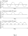
- Fig. 5 shows embodiments of half-wave and full-wave rectification of an RF signal. Using half-wave rectification implies that half of the signal is erased.
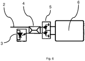
- FIG. 6 shows an embodiment of the present disclosure.
- a combined AM/FM encoded signal 2 is together with light from a local oscillator 3, combined into a coupler 4 into two electro-optical converters 5, which convert the signal into two electrical signals and passes them further into a rectifier 6, where the electrical signals are decoded.
- Example 7 Detuning of local oscillator using a photodiode with the same bandwidth as the bitrate of the system (back-to-back):
- Fig. 7 shows an example of how the bit error rate (BER) depends on the receiver input power for various local oscillator frequencies.
- the example as shown is modelled. In this example, the relationship is shown for a back-to-back.
- the bandwidth of the photodiode is 5GHz, which is equal to the bitrate of the system (5 Gbps).
- Optimum values of the LO frequency and drive amplitude are found. The drive amplitude is fixed at this optimum, and the LO frequency is varied around its optimum value. Accordingly, the receiver sensitivity at a BER of 10e-9 can for example be found for a given detuning.
- the opto-electrical converter in this case the photodiode, has a predefined frequency bandwidth.
- the predefined frequency bandwidth for the photodiode is proportional to the bitrate of system, and in this example, the proportionality factor is 1.
- Example 8 Detuning of local oscillator using a photodiode with a bandwidth of 1.5 times the bitrate of the system (back-to-back):
- Fig. 8 shows an example of how the bit error rate (BER) depends on the receiver input power for various local oscillator frequencies.
- the example as shown is modelled. In this example, the relationship is shown for a back-to-back.
- the bandwidth of the photodiode is 7.5GHz, which is 1.5 times the bitrate of the system (5 Gbps).
- Optimum values of the LO frequency and drive amplitude are found. The drive amplitude is fixed at this optimum, and the LO frequency is varied around its optimum value. Accordingly, the receiver sensitivity at a BER of 10e-9 can for example be found for a given detuning.
- the opto-electrical converter in this case the photodiode, has a predefined frequency bandwidth.
- the predefined frequency bandwidth for the photodiode is proportional to the bitrate of system, and in this example, the proportionality factor is 1.5.
- Example 9 Detuning of local oscillator using a photodiode with the same bandwidth as the bitrate of the system (100 km SSMF):
- Fig. 9 shows an example of how the bit error rate (BER) depends on the receiver input power for various local oscillator frequencies.
- the example as shown is modelled. In this example, the relationship is shown for a back-to-back.
- the bandwidth of the photodiode is 5GHz, which is equal to the bitrate of the system (5 Gbps).
- Optimum values of the LO frequency and drive amplitude are found. The drive amplitude is fixed at this optimum, and the LO frequency is varied around its optimum value. Accordingly, the receiver sensitivity at a BER of 10e-9 can for example be found for a given detuning.
- the opto-electrical converter in this case the photodiode, has a predefined frequency bandwidth.
- the predefined frequency bandwidth for the photodiode is proportional to the bitrate of system, and in this example, the proportionality factor is 1.
- Example 10 Detuning of local oscillator using a photodiode with a bandwidth of 1.5 times the bitrate of the system (100 km SSMF):
- Fig. 10 shows an example of how the bit error rate (BER) depends on the receiver input power for various local oscillator frequencies.
- the example as shown is modelled. In this example, the relationship is shown for a back-to-back.
- the bandwidth of the photodiode is 7.5GHz, which is 1.5 times the bitrate of the system (5 Gbps).
- Optimum values of the LO frequency and drive amplitude are found. The drive amplitude is fixed at this optimum, and the LO frequency is varied around its optimum value. Accordingly, the receiver sensitivity at a BER of 10e-9 can for example be found for a given detuning.
- the opto-electrical converter in this case the photodiode, has a predefined frequency bandwidth.
- the predefined frequency bandwidth for the photodiode is proportional to the bitrate of system, and in this example, the proportionality factor is 1.5.
- Fig. 11 shows an example of how the receiver sensitivity at a BER of 10e-9 depends on the LO detuning.
- the example as shown is modelled._In this example, the dependency is based on the data from Fig. 7-10 .
- This example shows that using a photodiode with a bandwidth of 1.5 times the bit rate of the system improves receiver sensitivity. This improvement is more pronounced in the low-dispersion (back-to-back) case.
- this example has shown that LO detuning is increased by increasing the photodiode bandwidth. Further, dispersion shifts the LO detuning from being symmetric around the optimum LO frequency towards being more tolerant to positive than to negative detuning values.
- the 1-dB tolerances are listed in the table below the graph.
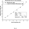
- Example 12 Frequency modulation (FM shift) vs VCSEL drive amplitude:
- Fig. 12 shows an example of how the FM shift depends on the peak-to-peak voltage of the data signal used to drive the VCSEL.
- the example as shown is modelled.
- the relationship is independent on the bitrate.
- Fig. 13 shows an example of how the AM extinction ratio depends on the peak-to-peak voltage of the data signal used to drive the VCSEL. The example as shown is modelled. As can be seen from the graph in Fig. 13 , there is a linear relationship between the AM extinction ratio and the drive amplitude of the VCSEL. It has been found that the relationship is independent on the bitrate.
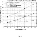
- Fig. 14 shows an example of the optimum drive amplitude and resultant FM shift at 5 Gbps back-to-back and after 100 km SSMF transmission as a function of PD bandwidth.
- the example as shown is modelled. It can be seen that for low dispersion (back-to-back), the optimum FM shift is almost equal to the bandwidth. For high dispersion (100 km SSMF), the optimum FM shift is almost constant with increasing PD bandwidth. The advantage of a high FM shift is countered by an increasing dispersion penalty due to the increased optical signal bandwidth for high FM shift.
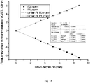
- Fig. 15 shown an example of how the frequency of the zero-level (F0) and one-level (F1) depends on the drive amplitude.
- the example as shown is modelled.
- Both F0 and F1 depend linearly on the drive amplitude.
- F1 moves towards higher frequencies, whereas F0 moves to lower frequencies.
- the center frequency in-between moves slightly towards lower frequencies. This is due the adiabatic chirp caused by the heating of the VCSEL due to the RMS power of the VCSEL drive signal.
- the center frequency shift is eliminated by temperature controlling VCSEL.
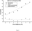
- Fig. 16 shows an example of how the optimum LO frequency-offset from the signal center frequency and F1 varies with the drive amplitude for a 5 Gbps and 7.5 Ghz photodiode (back-to-back).
- the example as shown is modelled. It can be seen that the LO should be tuned to have a constant offset from F1 irrespective of the drive amplitude and thereby also independent on the FM shift.
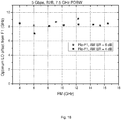
- Fig. 17 shows an example of how the optimum LO frequency-offset from the signal center frequency and F1 varies with the drive amplitude for a 5 Gbps and 7.5 GHz photodiode (100 km SSMF).
- the example as shown is modelled._It can be seen that the LO frequency is almost the same for all drive amplitudes and therefore for all values of the FM shift. In other words, this example shows the opposite of the example given in example 16. From this example, it can be seen that the optimum LO frequency is dependent dispersion.
- Example 18 Optimum LO frequency-offset from F1 as a function of FM shift using a photodiode bandwidth of 1.5 times the bitrate (back-to-back, 5Gbps):
- Fig. 18 shows how the optimum LO frequency-offset from F1 depends on the FM shift using a photodiode bandwidth of 1.5 times the bitrate for a back-to-back system.
- the example as shown is modelled. Results for different fixed AM extinction ratios are also included in the modelled results.
- the frequency of the local oscillator is selected to have a predefined offset from, preferably higher than, the frequency of one of the states in the encoded optical signal, preferably the state with the highest amplitude.
- the offset is dependent on the bandwidth of the opto-electrical converter. In this example, the bandwidth of the opto-electrical converter is 7.5 GHz, and the offset is between 7-9 GHz.
- the offset is selected to be between 0.9 and 1.2 times the bandwidth of the opto-electrical converter. From this example, it can be seen that optimum LO frequency-offset varies little with the FM shift. In other words, the offset is varying little in the range between approximately 1 and 1.5 times the bandwidth of the opto-electrical converter. In this example, it has been shown that for low dispersion, the optimum LO frequency-offset is independent of the AM extinction ration.
- Example 19 Optimum LO frequency-offset from F1 as a function of FM shift using a photodiode bandwidth of 2 times the bitrate (back-to-back, 5Gbps):
- Fig. 19 shows how the optimum LO frequency-offset from F1 depends on the FM shift using a photodiode bandwidth of 2 times the bitrate for a back-to-back system.
- the example as shown is modelled. Results for different fixed AM extinction ratios are also included in the modelled results.
- the frequency of the local oscillator is selected to have a predefined offset from, preferably higher than, the frequency of one of the states in the encoded optical signal, preferably the state with the highest amplitude.
- the offset is dependent on the bandwidth of the opto-electrical converter. In this example, the bandwidth of the opto-electrical converter is 10 GHz, and the offset is between 9.5-12.5 GHz.
- the offset is selected to be between 0.95 and 1.25 times the bandwidth of the opto-electrical converter. From this example, it can be seen that optimum LO frequency-offset varies little with the FM shift. In other words, the offset is varying little in the range between approximately 1 and 1.5 times the bandwidth of the opto-electrical converter. In this example, it has been shown that for low dispersion, the optimum LO frequency-offset is independent of the AM extinction ration.
- Example 20 Optimum LO frequency-offset from F1 as a function of FM shift using a photodiode bandwidth of 1.5 times the bitrate (40 km SSMF, 5Gbps):
- Fig. 20 shows how the optimum LO frequency-offset from F1 depends on the FM shift using a photodiode bandwidth of 1.5 times the bitrate for a 40 km SSMF system.
- the example as shown is modelled._Results for different fixed AM extinction ratios are also included in the modelled results.
- the frequency of the local oscillator is selected to have a predefined offset from, preferably higher than, the frequency of one of the states in the encoded optical signal, preferably the state with the highest amplitude.
- the offset is dependent on the bandwidth of the opto-electrical converter. In this example, the bandwidth of the opto-electrical converter is 7.5 GHz, and the offset is between ca. 7-10 GHz.
- the offset is selected to be between 0.9 and 1.35 times the bandwidth of the opto-electrical converter. From this example, it can be seen that optimum LO frequency-offset varies little with the FM shift. In other words, the offset is varying little in the range between approximately 1 and 1.5 times the bandwidth of the opto-electrical converter. In this example, it has been shown that for relatively low dispersion, the optimum LO frequency-offset is independent of the AM extinction ration.
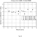
- Example 21 Optimum LO frequency-offset from F1 as a function of FM shift using a photodiode bandwidth of 2 times the bitrate (40 km SSMF, 5Gbps):
- Fig. 21 shows how the optimum LO frequency-offset from F1 depends on the FM shift using a photodiode bandwidth of 2 times the bitrate for a 40 km SSMF system.
- the example as shown is modelled._Results for different fixed AM extinction ratios are also included in the modelled results.
- the frequency of the local oscillator is selected to have a predefined offset from, preferably higher than, the frequency of one of the states in the encoded optical signal, preferably the state with the highest amplitude.
- the offset is dependent on the bandwidth of the opto-electrical converter. In this example, the bandwidth of the opto-electrical converter is 10 GHz, and the offset is between ca. 9-13 GHz.
- the offset is selected to be between 0.9 and 1.3 times the bandwidth of the opto-electrical converter. From this example, it can be seen that optimum LO frequency-offset varies little with the FM shift. In other words, the offset is varying little in the range between approximately 1 and 1.5 times the bandwidth of the opto-electrical converter. In this example, it has been shown that for relatively low dispersion, the optimum LO frequency-offset is independent of the AM extinction ration.
- Example 22 Optimum LO frequency-offset from F1 as a function of FM shift using a photodiode bandwidth of 1.5 times the bitrate (80 km SSMF, 5Gbps):
- Fig. 22 shows how the optimum LO frequency-offset from F1 depends on the FM shift using a photodiode bandwidth of 1.5 times the bitrate for a 80 km SSMF system.
- the example as shown is modelled. Results for different fixed AM extinction ratios are also included in the modelled results.
- the frequency of the local oscillator is selected to have a predefined offset from, preferably higher than, the frequency of one of the states in the encoded optical signal, preferably the state with the highest amplitude.
- the offset is dependent on the bandwidth of the opto-electrical converter. In this example, the bandwidth of the opto-electrical converter is 7.5 GHz, and the offset is between ca. 5-9 GHz.
- the offset is selected to be between 0.6 and 1.2 times the bandwidth of the opto-electrical converter. From this example, it can be seen that optimum LO frequency-offset varies little with the FM shift. In other words, the offset is in this example varying little in the range between approximately 0.5 and 1.5 times the bandwidth of the opto-electrical converter.
- Example 23 Optimum LO frequency-offset from F1 as a function of FM shift using a photodiode bandwidth of 2 times the bitrate (80 km SSMF, 5Gbps):
- Fig. 23 shows how the optimum LO frequency-offset from F1 depends on the FM shift using a photodiode bandwidth of 2 times the bitrate for a 80 km SSMF system.
- the example as shown is modelled. Results for different fixed AM extinction ratios are also included in the modelled results.
- the frequency of the local oscillator is selected to have a predefined offset from, preferably higher than, the frequency of one of the states in the encoded optical signal, preferably the state with the highest amplitude.
- the offset is dependent on the bandwidth of the opto-electrical converter. In this example, the bandwidth of the opto-electrical converter is 10 GHz, and the offset is between ca. 7-12 GHz.
- the offset is selected to be between 0.7 and 1.2 times the bandwidth of the opto-electrical converter. From this example, it can be seen that optimum LO frequency-offset varies little with the FM shift. In other words, the offset is in this example varying little in the range between approximately 0.5 and 1.5 times the bandwidth of the opto-electrical converter.
- Example 24 Optimum LO frequency-offset from F1 as a function of FM shift using a photodiode bandwidth of 1.5 times the bitrate (back-to-back, 10 Gbps):
- Fig. 24 shows how the optimum LO frequency-offset from F1 depends on the FM shift using a photodiode bandwidth of 1.5 times the bitrate for a back-to-back system.
- the example as shown is modelled. Results for different fixed AM extinction ratios are also included in the modelled results.
- the frequency of the local oscillator is selected to have a predefined offset from, preferably higher than, the frequency of one of the states in the encoded optical signal, preferably the state with the highest amplitude.
- the offset is dependent on the bandwidth of the opto-electrical converter. In this example, the bandwidth of the opto-electrical converter is 15 GHz, and the offset is between ca. 15-21 GHz.
- the offset is selected to be between 1 and 1.4 times the bandwidth of the opto-electrical converter. From this example, it can be seen that optimum LO frequency-offset varies little with the FM shift. In other words, the offset is in this example varying little in the range between 1 and 1.5 times the bandwidth of the opto-electrical converter.
- Example 25 Optimum LO frequency-offset from F1 as a function of FM shift using a photodiode bandwidth of 2 times the bitrate (back-to-back, 10Gbps):
- Fig. 25 shows how the optimum LO frequency-offset from F1 depends on the FM shift using a photodiode bandwidth of 2 times the bitrate for a back-to-back system.
- the example as shown is modelled. Results for different fixed AM extinction ratios are also included in the modelled results.
- the frequency of the local oscillator is selected to have a predefined offset from, preferably higher than, the frequency of one of the states in the encoded optical signal, preferably the state with the highest amplitude.
- the offset is dependent on the bandwidth of the opto-electrical converter. In this example, the bandwidth of the opto-electrical converter is 20 GHz, and the offset is between ca. 18-29 GHz.
- the offset is selected to be between 0.9 and 1.5 times the bandwidth of the opto-electrical converter. From this example, it can be seen that optimum LO frequency-offset varies little with the FM shift. In other words, the offset is in this example varying little in the range between approximately 1 and 1.5 times the bandwidth of the opto-electrical converter.
- Example 26 Optimum LO frequency-offset from F1 as a function of FM shift using a photodiode bandwidth of 1.5 times the bitrate (40 km SSMF, 10Gbps):
- Fig. 26 shows how the optimum LO frequency-offset from F1 depends on the FM shift using a photodiode bandwidth of 1.5 times the bitrate for a 40 km SSMF system.
- the example as shown is modelled. Results for different fixed AM extinction ratios are also included in the modelled results.
- the frequency of the local oscillator is selected to have a predefined offset from, preferably higher than, the frequency of one of the states in the encoded optical signal, preferably the state with the highest amplitude.
- the offset is dependent on the bandwidth of the opto-electrical converter. In this example, the bandwidth of the opto-electrical converter is 15 GHz, and the offset is between ca. 13-21 GHz.
- the offset is selected to be between roughly 0.9 and 1.4 times the bandwidth of the opto-electrical converter. From this example, it can be seen that optimum LO frequency-offset varies little with the FM shift. In other words, the offset is in this example varying little in the range between approximately 1 and 1.5 times the bandwidth of the opto-electrical converter.
- Example 27 Optimum LO frequency-offset from F1 as a function of FM shift using a photodiode bandwidth of 2 times the bitrate (40 km SSMF, 10Gbps):
- Fig. 27 shows how the optimum LO frequency-offset from F1 depends on the FM shift using a photodiode bandwidth of 2 times the bitrate for a 40 km SSMF system.
- the example as shown is modelled. Results for different fixed AM extinction ratios are also included in the modelled results.
- the frequency of the local oscillator is selected to have a predefined offset from, preferably higher than, the frequency of one of the states in the encoded optical signal, preferably the state with the highest amplitude.
- the offset is dependent on the bandwidth of the opto-electrical converter. In this example, the bandwidth of the opto-electrical converter is 20 GHz, and the offset is between ca. 22-32 GHz.
- the offset is selected to be between roughly 1.1 and 1.6 times the bandwidth of the opto-electrical converter. From this example, it can be seen that optimum LO frequency-offset varies little with the FM shift. In other words, the offset is in this example varying little in the range between approximately 1 and 1.6 times the bandwidth of the opto-electrical converter.
- Example 28 Optimum FM shift as a function of photo-detector bandwidth and transmission distance (5 Gbps):
- Fig. 28 shows an example of how the optimum FM shift depends on the photo-detector bandwidth and transmission distance for 5 Gbps systems.
- the frequency modulation is configured such that the frequency separation between the states in the optical signal is dependent on the frequency bandwidth of the opto-electrical converter, in particular the frequency modulation is configured such that the frequency separation between the states in the optical signal is proportional with a proportionality factor to the frequency bandwidth of the opto-electrical converter.
- the proportionality factor is approximately 1.2
- the proportionality factor is approximately 1
- for a 80 km SSMF system the proportionality factor is approximately 0.8.
- dispersion decreases the optimum FM-shift.
- Fig. 29 shows an example of how the optimum FM shift depends on the photo-detector bandwidth and transmission distance for 10 Gbps systems.
- the frequency modulation is configured such that the frequency separation between the states in the optical signal is dependent on the frequency bandwidth of the opto-electrical converter
- the frequency modulation is configured such that the frequency separation between the states in the optical signal is proportional with a proportionality factor to the frequency bandwidth of the opto-electrical converter.
- the proportionality factor is approximately 0.8
- the proportionality factor is approximately 0.4.
Landscapes
- Physics & Mathematics (AREA)
- Electromagnetism (AREA)
- Engineering & Computer Science (AREA)
- Computer Networks & Wireless Communication (AREA)
- Signal Processing (AREA)
- Optical Communication System (AREA)
- Synchronisation In Digital Transmission Systems (AREA)
Claims (27)
- Verfahren zur Dekodierung eines kodierten optischen Signals (2), umfassend mindestens zwei unterschiedliche Zustände, wie etwa "0"-Zustände (0) und "1"-Zustände (1), wobei das optische Signal frequenz- und amplitudenmoduliert ist, sodass die unterschiedlichen Zustände in Frequenz und Amplitude getrennt sind, wobei das Verfahren die folgenden Schritte umfasst:• Kombinieren des kodierten optischen Signals mit Licht von einem Lokaloszillator (3), der mit einer Lokaloszillatorfrequenz konfiguriert ist;• Umwandeln des kombinierten Lokaloszillators und des kodierten optischen Signals in ein oder mehrere elektrische Signale mithilfe von mindestens einem optoelektrischen Wandler (5), der eine vordefinierte Frequenzbandbreite aufweist, wodurch ein verstärktes und kodiertes elektrisches Signal bereitgestellt wird, das einen kodierten Signalstrom oder mehrere kodierte Signalströme aufweist, wobei eine Art von Zuständen eine höhere Schwingfrequenz aufweist als eine andere Art von Zuständen;• Gleichrichten des kodierten Signalstroms bzw. der kodierten Signalströme, wodurch ein kodiertes Leistungsspektrum erhalten wird, wobei das Leistungsspektrum unterschiedliche Zustände, wie etwa "0"-Zustände (0) und "1"-Zustände (1), mit unterschiedlichen Leistungspegeln aufweist, sodass sie unterschieden werden können,wobei die Lokaloszillatorfrequenz durch einen positiven Lokaloszillatorfrequenzversatz von der Frequenz von einem der Zustände in dem kodierten optischen Signal definiert ist, dadurch gekennzeichnet, dass
der Lokaloszillatorfrequenzversatz so ausgewählt ist, dass er zwischen dem 1- und 1,5-Fachen der vordefinierten Frequenzbandbreite des optoelektrischen Wandlers (5) liegt. - Verfahren nach Anspruch 1, wobei das Leistungsspektrum durch einen Tiefpassfilter gefiltert wird, wodurch die Restleistung von einer Art von Zuständen in Bezug auf eine andere Art eines Zustands verringert wird.
- Verfahren nach einem der vorhergehenden Ansprüche, wobei das Leistungsspektrum mit einer Schwellendetektion angewendet wird, sodass unterschiedliche Zustände, wie etwa "0"-Zustände (0) und "1"-Zustände (1), automatisch detektiert werden.
- Verfahren nach einem der vorhergehenden Ansprüche, wobei der eine der Zustände ein Zustand mit der höchsten Amplitude ist.
- Verfahren nach einem der vorhergehenden Ansprüche, wobei der Lokaloszillator (3) ohne eine Phasenregelschleife betrieben wird.
- Verfahren nach einem der vorhergehenden Ansprüche, wobei der Lokaloszillatorfrequenzversatz größer ist als die Bandbreite des optoelektrischen Wandlers (5).
- Verfahren nach einem der vorhergehenden Ansprüche, wobei der Lokaloszillatorfrequenzversatz ausgewählt ist, um etwa dem 1,2-Fachen der Bandbreite des optoelektrischen Wandlers (5) zu entsprechen.
- Verfahren zum Übertragen eines optischen Signals, umfassend die folgenden Schritte:• Kodieren des optischen Signals durch eine Amplituden- und Frequenzmodulation, und• Dekodieren des kombinierten AM- und FM-Signals nach einem der Ansprüche 1-7,und wobei bei dem Kodieren oder Dekodieren eines kombinierten AM- und FM-Signals zwei oder mehr Pegel verwendet werden.
- Verfahren nach Anspruch 8, wobei das Signal durch eine oder mehrere simultane AM- und FM-Vorrichtungen, wie etwa einen frequenzgechirpten Laser, insbesondere einen DML oder VCSEL, kodiert wird.
- Verfahren nach Anspruch 8, wobei das Signal durch eine oder mehrere getrennte AM-Vorrichtung(en) und eine oder mehrere getrennte FM-Vorrichtung(en) kodiert wird.
- Verfahren nach einem der vorhergehenden Ansprüche 8-10, wobei das optische Signal mit einem AM-Extinktionsverhältnis zwischen 3 dB und 6 dB, vorzugsweise zwischen 4 dB und 5 dB, vorzugsweiser etwa 4,5 dB konfiguriert ist.
- Verfahren nach einem der vorhergehenden Ansprüche 8-11, wobei die Frequenzmodulation so konfiguriert ist, dass die Frequenztrennung zwischen den Zuständen in dem optischen Signal kleiner ist als 15 GHz, oder kleiner als 14 GHz, oder kleiner als 13 GHz, oder kleiner als 12 GHz, oder kleiner als 11 GHz, oder kleiner als 10 GHz.
- Verfahren nach einem der vorhergehenden Ansprüche 8-12, wobei die Frequenzmodulation so konfiguriert ist, dass die Frequenztrennung zwischen den Zuständen in dem optischen Signal von der Frequenzbandbreite des optoelektrischen Wandlers abhängt.
- Verfahren nach einem der vorhergehenden Ansprüche 8-13, wobei die Frequenzmodulation so konfiguriert ist, dass die Frequenztrennung zwischen den Zuständen in dem optischen Signal mit einem Proportionalitätsfaktor zu der Frequenzbandbreite des optoelektrischen Wandlers (5) proportional ist.
- Verfahren nach Anspruch 14, wobei der Proportionalitätsfaktor zwischen 0,2 und 1,4, wie etwa zwischen 0,4 und 1,2, wie etwa zwischen 0,8 und 1,2, wie etwa zwischen 0,9 und 1,1, wie etwa bei 1, liegt.
- Detektorsystem zur Dekodierung eines kombinierten kodierten optischen AM- und FM-Signals (2), umfassend mindestens zwei unterschiedliche Arten von Zuständen, wie etwa "0"-Zustände (0) und "1"-Zustände (1), umfassend:• einen Lokaloszillator (3), der mit einer Lokaloszillatorfrequenz konfiguriert ist;• eine Kopplungsvorrichtung (4), die konfiguriert ist, um das kodierte optische Signal (2) mit Licht von dem Lokaloszillator zu koppeln;• einen oder mehrere optoelektrische Wandler (5), die eine vordefinierte Frequenzbandbreite aufweisen, die konfiguriert sind, um ein verstärktes und kodiertes elektrisches Signal bereitzustellen, das einen kodierten Signalstrom oder mehrere kodierte Signalströme aufweist, wobei eine Art von Zuständen eine höhere Schwingfrequenz aufweist als eine andere Art von Zuständen;• einen Gleichrichter (6), der für eine Gleichrichtung des Signalstroms bzw. der Signalströme konfiguriert ist, um ein Leistungsspektrum bereitzustellen, wobei das Leistungsspektrum unterschiedliche Zustände, wie etwa "0"-Zustände (0) und "1"-Zustände (1), mit unterschiedlichen Leistungspegeln aufweist, sodass sie unterschieden werden können,wobei die Lokaloszillatorfrequenz durch einen positiven Lokaloszillatorfrequenzversatz von der Frequenz von einem der Zustände in dem kodierten optischen Signal definiert ist, dadurch gekennzeichnet, dass
der Lokaloszillatorfrequenzversatz so ausgewählt ist, dass er zwischen dem 1- und 1,5-Fachen der vordefinierten Frequenzbandbreite des optoelektrischen Wandlers (5) liegt. - Detektorsystem nach Anspruch 16, ferner umfassend einen Tiefpassfilter, der konfiguriert ist, um die Restleistung von einer Art von Zuständen in Bezug auf eine andere Art eines Zustands zu verringern, sodass "0"-Zustände (0) und "1"-Zustände (1) mit unterschiedlichen Leistungspegeln einfacher unterschieden werden können.
- Detektorsystem nach Ansprüche 16-17, ferner umfassend ein Schwellendetektionsmodul, das für die Schwellendetektion des Leistungsspektrums konfiguriert ist, sodass unterschiedliche Zustände, wie etwa "0"-Zustände (0) und "1"-Zustände (1), automatisch detektiert werden.
- Detektorsystem nach Ansprüche 17-18, wobei der Lokaloszillator (3) ein ungekühlter Laser, wie etwa ein DML und/oder VCSEL, ist.
- Detektorsystem nach Ansprüche 17-18, wobei der Lokaloszillator (3) ein temperaturgesteuerter Laser, wie etwa ein DML und/oder VCSEL, ist.
- Detektorsystem nach Ansprüche 16-20, wobei der eine der Zustände ein Zustand mit der höchsten Amplitude ist.
- Detektorsystem nach Ansprüche 16-21, wobei der Lokaloszillatorfrequenzversatz größer ist als die Bandbreite des optoelektrischen Wandlers bzw. der optoelektrischen Wandler (5).
- Detektorsystem nach Ansprüche 16-21, wobei der Lokaloszillatorfrequenzversatz ausgewählt ist, um etwa dem 1,2-Fachen der Bandbreite des optoelektrischen Wandlers bzw. der optoelektrischen Wandler (5) zu entsprechen.
- Optisches Kommunikationssystem, umfassend mindestens einen Sender und mindestens einen Empfänger, umfassend das Detektorsystem nach einem der Ansprüche 16-23.
- Optisches Kommunikationssystem nach Anspruch 24, wobei der Sender konfiguriert ist, um ein kombiniertes AM- und FM-Signal durch eine oder mehrere kombinierte AM- und FM-Vorrichtung(en), wie etwa einen frequenzgechirpten Laser, insbesondere einen DML oder einen VCSEL, zu generieren.
- Optisches Kommunikationssystem nach Ansprüche 24-25, wobei der Sender konfiguriert ist, um ein kombiniertes AM-und FM-Signal durch eine oder mehrere getrennte AM-Vorrichtungen und durch eine oder mehrere getrennte FM-Vorrichtungen zu generieren.
- Optisches Kommunikationssystem nach Ansprüche 24-26, wobei der Sender konfiguriert ist, um das Verfahren nach einem der Ansprüche 8-15 durchzuführen und/oder wobei der Empfänger konfiguriert ist, um das Verfahren nach einem der Ansprüche 1-7 durchzuführen.
Priority Applications (2)
| Application Number | Priority Date | Filing Date | Title |
|---|---|---|---|
| EP18162794.4A EP3399671A1 (de) | 2014-02-07 | 2015-02-06 | Decodierung eines kombinierten amplitudenmodulierten und frequenzmodulierten signals |
| PL15702811T PL3103202T3 (pl) | 2014-02-07 | 2015-02-06 | Dekodowanie sygnału modulowanego metodą połączonej modulacji amplitudy i częstotliwości |
Applications Claiming Priority (2)
| Application Number | Priority Date | Filing Date | Title |
|---|---|---|---|
| EP14154237 | 2014-02-07 | ||
| PCT/EP2015/052535 WO2015118118A1 (en) | 2014-02-07 | 2015-02-06 | Decoding a combined amplitude modulated and frequency modulated signal |
Related Child Applications (1)
| Application Number | Title | Priority Date | Filing Date |
|---|---|---|---|
| EP18162794.4A Division EP3399671A1 (de) | 2014-02-07 | 2015-02-06 | Decodierung eines kombinierten amplitudenmodulierten und frequenzmodulierten signals |
Publications (2)
| Publication Number | Publication Date |
|---|---|
| EP3103202A1 EP3103202A1 (de) | 2016-12-14 |
| EP3103202B1 true EP3103202B1 (de) | 2018-03-21 |
Family
ID=50070389
Family Applications (2)
| Application Number | Title | Priority Date | Filing Date |
|---|---|---|---|
| EP15702811.9A Active EP3103202B1 (de) | 2014-02-07 | 2015-02-06 | Dekodierung eines kombinierten amplitudenmodulierten und frequenzmodulierten signals |
| EP18162794.4A Ceased EP3399671A1 (de) | 2014-02-07 | 2015-02-06 | Decodierung eines kombinierten amplitudenmodulierten und frequenzmodulierten signals |
Family Applications After (1)
| Application Number | Title | Priority Date | Filing Date |
|---|---|---|---|
| EP18162794.4A Ceased EP3399671A1 (de) | 2014-02-07 | 2015-02-06 | Decodierung eines kombinierten amplitudenmodulierten und frequenzmodulierten signals |
Country Status (13)
| Country | Link |
|---|---|
| US (2) | US10014952B2 (de) |
| EP (2) | EP3103202B1 (de) |
| JP (1) | JP6706205B2 (de) |
| CN (1) | CN106134108B (de) |
| BR (1) | BR112016018210B1 (de) |
| CA (1) | CA2937056C (de) |
| DK (1) | DK3103202T3 (de) |
| ES (1) | ES2671781T3 (de) |
| MX (1) | MX361685B (de) |
| PL (1) | PL3103202T3 (de) |
| PT (1) | PT3103202T (de) |
| RU (1) | RU2668279C2 (de) |
| WO (1) | WO2015118118A1 (de) |
Families Citing this family (7)
| Publication number | Priority date | Publication date | Assignee | Title |
|---|---|---|---|---|
| EP3103202B1 (de) * | 2014-02-07 | 2018-03-21 | Danmarks Tekniske Universitet | Dekodierung eines kombinierten amplitudenmodulierten und frequenzmodulierten signals |
| WO2016161638A1 (zh) * | 2015-04-10 | 2016-10-13 | 华为技术有限公司 | 一种相干光源频偏估计和补偿的相干接收机、方法和系统 |
| US9960846B2 (en) * | 2015-07-14 | 2018-05-01 | LGS Innovations LLC | Free-space optical communication system and method in scattering environments |
| KR20190127783A (ko) | 2017-03-21 | 2019-11-13 | 비프로스트 커뮤니케이션즈 에이피에스 | 고성능 광수신기를 포함한 광학 통신 시스템, 장치 및 방법 |
| CN113132020B (zh) * | 2019-12-31 | 2023-07-28 | 华为技术有限公司 | 相干光接收装置和采用相干光接收装置的光系统 |
| EP4282093B1 (de) * | 2021-01-20 | 2025-02-12 | Danmarks Tekniske Universitet | Direkte detektion von modulierten kohärenten optischen signalen mittels einer struktur mit fano-resonanz |
| US11848703B2 (en) * | 2021-09-21 | 2023-12-19 | Apple Inc. | Communication devices and methods for direct detection and photonics receiver |
Family Cites Families (21)
| Publication number | Priority date | Publication date | Assignee | Title |
|---|---|---|---|---|
| US14952A (en) * | 1856-05-27 | Thegraphio co | ||
| AU551885B2 (en) | 1983-11-15 | 1986-05-15 | Yoshida Kogyo K.K. | Recovery of scrap thermoplastics |
| US4759080A (en) * | 1983-11-16 | 1988-07-19 | Nec Corporation | Coherent optical communication system with FSK heterodyne or homodyne detection and little influence by distortion of a modulated optical signal |
| JPS60107626A (ja) * | 1983-11-16 | 1985-06-13 | Nec Corp | 光ヘテロダイン・ホモダイン通信方法 |
| JPS6149530A (ja) * | 1984-08-17 | 1986-03-11 | Nec Corp | 光ヘテロダイン通信方法 |
| GB2172766B (en) | 1985-03-21 | 1988-12-21 | Stc Plc | Optical receiver |
| DE3621734A1 (de) | 1986-06-28 | 1988-01-07 | Standard Elektrik Lorenz Ag | Optischer ueberlagerungsempfaenger |
| US4829598A (en) | 1987-01-22 | 1989-05-09 | Siemens Aktiengesellschaft | Optical receiver with an optical coupler and an electronic amplifier |
| JPH02162330A (ja) | 1988-12-16 | 1990-06-21 | Hitachi Ltd | 偏波ダイバシティ光受信方法とその装置および中間周波数安定化方法 |
| RU2097927C1 (ru) * | 1995-05-31 | 1997-11-27 | Евгений Григорьевич Крапошин | Система передачи информации |
| US5760941A (en) * | 1996-02-29 | 1998-06-02 | Rice University | System and method for performing optical code division multiple access communication using bipolar codes |
| RU2124236C1 (ru) * | 1997-01-22 | 1998-12-27 | Тульский государственный университет | Способ воспроизведения информации |
| EP1249112B1 (de) * | 2000-01-17 | 2009-03-25 | Broadcom Corporation | Hochgeschwindigkeitsübertragungssystem für optische kanäle |
| US7373091B2 (en) | 2003-09-25 | 2008-05-13 | Lucent Technologies Inc. | Multicasting optical switch fabric and method of detection based on novel heterodyne receiver |
| US7747169B2 (en) * | 2006-12-22 | 2010-06-29 | Alcatel-Lucent Usa Inc. | Adaptive polarization tracking and equalization in coherent optical receivers |
| JP5278001B2 (ja) * | 2009-01-29 | 2013-09-04 | 富士通株式会社 | 光通信システムおよび光受信器 |
| CN101938438B (zh) | 2009-06-30 | 2014-02-19 | 华为技术有限公司 | 一种光信号产生和接收的方法、装置和光传输系统 |
| WO2012153220A1 (en) * | 2011-05-06 | 2012-11-15 | Koninklijke Philips Electronics N.V. | Lighting device and receiver |
| US9136948B2 (en) | 2011-07-27 | 2015-09-15 | Cisco Technology, Inc. | Electrical modulator driver circuit for generating multi-level drive signals for QAM optical transmission |
| JP6010955B2 (ja) * | 2012-03-22 | 2016-10-19 | 日本電気株式会社 | コヒーレント光受信機および光受信方法 |
| EP3103202B1 (de) * | 2014-02-07 | 2018-03-21 | Danmarks Tekniske Universitet | Dekodierung eines kombinierten amplitudenmodulierten und frequenzmodulierten signals |
-
2015
- 2015-02-06 EP EP15702811.9A patent/EP3103202B1/de active Active
- 2015-02-06 US US15/117,048 patent/US10014952B2/en active Active
- 2015-02-06 CN CN201580007636.1A patent/CN106134108B/zh active Active
- 2015-02-06 MX MX2016010129A patent/MX361685B/es active IP Right Grant
- 2015-02-06 WO PCT/EP2015/052535 patent/WO2015118118A1/en not_active Ceased
- 2015-02-06 PL PL15702811T patent/PL3103202T3/pl unknown
- 2015-02-06 RU RU2016132119A patent/RU2668279C2/ru active
- 2015-02-06 DK DK15702811.9T patent/DK3103202T3/en active
- 2015-02-06 CA CA2937056A patent/CA2937056C/en active Active
- 2015-02-06 ES ES15702811.9T patent/ES2671781T3/es active Active
- 2015-02-06 EP EP18162794.4A patent/EP3399671A1/de not_active Ceased
- 2015-02-06 BR BR112016018210-3A patent/BR112016018210B1/pt active IP Right Grant
- 2015-02-06 PT PT157028119T patent/PT3103202T/pt unknown
- 2015-02-06 JP JP2016550765A patent/JP6706205B2/ja active Active
-
2018
- 2018-05-29 US US15/991,762 patent/US10516488B2/en active Active
Also Published As
| Publication number | Publication date |
|---|---|
| ES2671781T3 (es) | 2018-06-08 |
| PL3103202T3 (pl) | 2018-07-31 |
| MX2016010129A (es) | 2017-04-06 |
| EP3103202A1 (de) | 2016-12-14 |
| RU2016132119A3 (de) | 2018-05-17 |
| CA2937056A1 (en) | 2015-08-13 |
| US10014952B2 (en) | 2018-07-03 |
| RU2016132119A (ru) | 2018-03-13 |
| RU2668279C2 (ru) | 2018-09-28 |
| US20180278338A1 (en) | 2018-09-27 |
| EP3399671A1 (de) | 2018-11-07 |
| CA2937056C (en) | 2021-04-06 |
| CN106134108B (zh) | 2019-12-24 |
| JP6706205B2 (ja) | 2020-06-03 |
| PT3103202T (pt) | 2018-06-06 |
| WO2015118118A1 (en) | 2015-08-13 |
| BR112016018210A2 (pt) | 2017-08-08 |
| BR112016018210B1 (pt) | 2023-11-21 |
| DK3103202T3 (en) | 2018-06-14 |
| US10516488B2 (en) | 2019-12-24 |
| US20160352432A1 (en) | 2016-12-01 |
| MX361685B (es) | 2018-12-13 |
| CN106134108A (zh) | 2016-11-16 |
| JP2017511032A (ja) | 2017-04-13 |
Similar Documents
| Publication | Publication Date | Title |
|---|---|---|
| US10516488B2 (en) | Decoding a combined amplitude modulated and frequency modulated signal | |
| US10608747B2 (en) | Optical communication systems, devices, and methods including high performance optical receivers | |
| EP1727301B1 (de) | Optisches üebrtragungssystem, optische übertragungseinrichtung und optische empfangseinrichtung eines optischen übertragungssystems | |
| CN110380779A (zh) | 用于脉冲振幅调制信号的振幅相干检测 | |
| JP2011514771A (ja) | 光学レシーバのための位相制御回路及び方法 | |
| US8373921B2 (en) | Methods and systems for modulating and demodulating millimeter-wave signals | |
| Forestieri et al. | High-speed optical communications systems for future WDM centralized radio access networks | |
| EP3155733B1 (de) | Optischer sendeempfänger | |
| Kasai et al. | The use of a Nyquist filter for reducing an optical signal bandwidth in a coherent QAM optical transmission | |
| Xu et al. | Coherent Optics for Access Networks: From P2P to P2MP | |
| HK40014239B (en) | Optical communication systems, devices, and methods including high performance optical receivers | |
| HK40014239A (en) | Optical communication systems, devices, and methods including high performance optical receivers |
Legal Events
| Date | Code | Title | Description |
|---|---|---|---|
| PUAI | Public reference made under article 153(3) epc to a published international application that has entered the european phase |
Free format text: ORIGINAL CODE: 0009012 |
|
| STAA | Information on the status of an ep patent application or granted ep patent |
Free format text: STATUS: REQUEST FOR EXAMINATION WAS MADE |
|
| 17P | Request for examination filed |
Effective date: 20160907 |
|
| AK | Designated contracting states |
Kind code of ref document: A1 Designated state(s): AL AT BE BG CH CY CZ DE DK EE ES FI FR GB GR HR HU IE IS IT LI LT LU LV MC MK MT NL NO PL PT RO RS SE SI SK SM TR |
|
| AX | Request for extension of the european patent |
Extension state: BA ME |
|
| DAX | Request for extension of the european patent (deleted) | ||
| GRAP | Despatch of communication of intention to grant a patent |
Free format text: ORIGINAL CODE: EPIDOSNIGR1 |
|
| STAA | Information on the status of an ep patent application or granted ep patent |
Free format text: STATUS: GRANT OF PATENT IS INTENDED |
|
| INTG | Intention to grant announced |
Effective date: 20170912 |
|
| GRAS | Grant fee paid |
Free format text: ORIGINAL CODE: EPIDOSNIGR3 |
|
| GRAA | (expected) grant |
Free format text: ORIGINAL CODE: 0009210 |
|
| STAA | Information on the status of an ep patent application or granted ep patent |
Free format text: STATUS: THE PATENT HAS BEEN GRANTED |
|
| AK | Designated contracting states |
Kind code of ref document: B1 Designated state(s): AL AT BE BG CH CY CZ DE DK EE ES FI FR GB GR HR HU IE IS IT LI LT LU LV MC MK MT NL NO PL PT RO RS SE SI SK SM TR |
|
| REG | Reference to a national code |
Ref country code: GB Ref legal event code: FG4D |
|
| REG | Reference to a national code |
Ref country code: CH Ref legal event code: EP |
|
| REG | Reference to a national code |
Ref country code: AT Ref legal event code: REF Ref document number: 982178 Country of ref document: AT Kind code of ref document: T Effective date: 20180415 |
|
| REG | Reference to a national code |
Ref country code: IE Ref legal event code: FG4D |
|
| REG | Reference to a national code |
Ref country code: DE Ref legal event code: R096 Ref document number: 602015009080 Country of ref document: DE |
|
| REG | Reference to a national code |
Ref country code: PT Ref legal event code: SC4A Ref document number: 3103202 Country of ref document: PT Date of ref document: 20180606 Kind code of ref document: T Free format text: AVAILABILITY OF NATIONAL TRANSLATION Effective date: 20180529 |
|
| REG | Reference to a national code |
Ref country code: ES Ref legal event code: FG2A Ref document number: 2671781 Country of ref document: ES Kind code of ref document: T3 Effective date: 20180608 |
|
| REG | Reference to a national code |
Ref country code: DK Ref legal event code: T3 Effective date: 20180608 |
|
| REG | Reference to a national code |
Ref country code: SE Ref legal event code: TRGR |
|
| REG | Reference to a national code |
Ref country code: NL Ref legal event code: MP Effective date: 20180321 |
|
| PG25 | Lapsed in a contracting state [announced via postgrant information from national office to epo] |
Ref country code: HR Free format text: LAPSE BECAUSE OF FAILURE TO SUBMIT A TRANSLATION OF THE DESCRIPTION OR TO PAY THE FEE WITHIN THE PRESCRIBED TIME-LIMIT Effective date: 20180321 Ref country code: NO Free format text: LAPSE BECAUSE OF FAILURE TO SUBMIT A TRANSLATION OF THE DESCRIPTION OR TO PAY THE FEE WITHIN THE PRESCRIBED TIME-LIMIT Effective date: 20180621 Ref country code: FI Free format text: LAPSE BECAUSE OF FAILURE TO SUBMIT A TRANSLATION OF THE DESCRIPTION OR TO PAY THE FEE WITHIN THE PRESCRIBED TIME-LIMIT Effective date: 20180321 Ref country code: LT Free format text: LAPSE BECAUSE OF FAILURE TO SUBMIT A TRANSLATION OF THE DESCRIPTION OR TO PAY THE FEE WITHIN THE PRESCRIBED TIME-LIMIT Effective date: 20180321 Ref country code: CY Free format text: LAPSE BECAUSE OF FAILURE TO SUBMIT A TRANSLATION OF THE DESCRIPTION OR TO PAY THE FEE WITHIN THE PRESCRIBED TIME-LIMIT Effective date: 20180321 |
|
| REG | Reference to a national code |
Ref country code: LT Ref legal event code: MG4D |
|
| REG | Reference to a national code |
Ref country code: AT Ref legal event code: MK05 Ref document number: 982178 Country of ref document: AT Kind code of ref document: T Effective date: 20180321 |
|
| PG25 | Lapsed in a contracting state [announced via postgrant information from national office to epo] |
Ref country code: LV Free format text: LAPSE BECAUSE OF FAILURE TO SUBMIT A TRANSLATION OF THE DESCRIPTION OR TO PAY THE FEE WITHIN THE PRESCRIBED TIME-LIMIT Effective date: 20180321 Ref country code: GR Free format text: LAPSE BECAUSE OF FAILURE TO SUBMIT A TRANSLATION OF THE DESCRIPTION OR TO PAY THE FEE WITHIN THE PRESCRIBED TIME-LIMIT Effective date: 20180622 Ref country code: RS Free format text: LAPSE BECAUSE OF FAILURE TO SUBMIT A TRANSLATION OF THE DESCRIPTION OR TO PAY THE FEE WITHIN THE PRESCRIBED TIME-LIMIT Effective date: 20180321 Ref country code: BG Free format text: LAPSE BECAUSE OF FAILURE TO SUBMIT A TRANSLATION OF THE DESCRIPTION OR TO PAY THE FEE WITHIN THE PRESCRIBED TIME-LIMIT Effective date: 20180621 |
|
| PG25 | Lapsed in a contracting state [announced via postgrant information from national office to epo] |
Ref country code: RO Free format text: LAPSE BECAUSE OF FAILURE TO SUBMIT A TRANSLATION OF THE DESCRIPTION OR TO PAY THE FEE WITHIN THE PRESCRIBED TIME-LIMIT Effective date: 20180321 Ref country code: EE Free format text: LAPSE BECAUSE OF FAILURE TO SUBMIT A TRANSLATION OF THE DESCRIPTION OR TO PAY THE FEE WITHIN THE PRESCRIBED TIME-LIMIT Effective date: 20180321 Ref country code: AL Free format text: LAPSE BECAUSE OF FAILURE TO SUBMIT A TRANSLATION OF THE DESCRIPTION OR TO PAY THE FEE WITHIN THE PRESCRIBED TIME-LIMIT Effective date: 20180321 Ref country code: NL Free format text: LAPSE BECAUSE OF FAILURE TO SUBMIT A TRANSLATION OF THE DESCRIPTION OR TO PAY THE FEE WITHIN THE PRESCRIBED TIME-LIMIT Effective date: 20180321 |
|
| PG25 | Lapsed in a contracting state [announced via postgrant information from national office to epo] |
Ref country code: AT Free format text: LAPSE BECAUSE OF FAILURE TO SUBMIT A TRANSLATION OF THE DESCRIPTION OR TO PAY THE FEE WITHIN THE PRESCRIBED TIME-LIMIT Effective date: 20180321 Ref country code: CZ Free format text: LAPSE BECAUSE OF FAILURE TO SUBMIT A TRANSLATION OF THE DESCRIPTION OR TO PAY THE FEE WITHIN THE PRESCRIBED TIME-LIMIT Effective date: 20180321 Ref country code: SK Free format text: LAPSE BECAUSE OF FAILURE TO SUBMIT A TRANSLATION OF THE DESCRIPTION OR TO PAY THE FEE WITHIN THE PRESCRIBED TIME-LIMIT Effective date: 20180321 Ref country code: SM Free format text: LAPSE BECAUSE OF FAILURE TO SUBMIT A TRANSLATION OF THE DESCRIPTION OR TO PAY THE FEE WITHIN THE PRESCRIBED TIME-LIMIT Effective date: 20180321 |
|
| REG | Reference to a national code |
Ref country code: DE Ref legal event code: R097 Ref document number: 602015009080 Country of ref document: DE |
|
| PLBE | No opposition filed within time limit |
Free format text: ORIGINAL CODE: 0009261 |
|
| STAA | Information on the status of an ep patent application or granted ep patent |
Free format text: STATUS: NO OPPOSITION FILED WITHIN TIME LIMIT |
|
| 26N | No opposition filed |
Effective date: 20190102 |
|
| PG25 | Lapsed in a contracting state [announced via postgrant information from national office to epo] |
Ref country code: IT Free format text: LAPSE BECAUSE OF FAILURE TO SUBMIT A TRANSLATION OF THE DESCRIPTION OR TO PAY THE FEE WITHIN THE PRESCRIBED TIME-LIMIT Effective date: 20180321 |
|
| PG25 | Lapsed in a contracting state [announced via postgrant information from national office to epo] |
Ref country code: SI Free format text: LAPSE BECAUSE OF FAILURE TO SUBMIT A TRANSLATION OF THE DESCRIPTION OR TO PAY THE FEE WITHIN THE PRESCRIBED TIME-LIMIT Effective date: 20180321 |
|
| REG | Reference to a national code |
Ref country code: CH Ref legal event code: PL |
|
| PG25 | Lapsed in a contracting state [announced via postgrant information from national office to epo] |
Ref country code: MC Free format text: LAPSE BECAUSE OF FAILURE TO SUBMIT A TRANSLATION OF THE DESCRIPTION OR TO PAY THE FEE WITHIN THE PRESCRIBED TIME-LIMIT Effective date: 20180321 Ref country code: LU Free format text: LAPSE BECAUSE OF NON-PAYMENT OF DUE FEES Effective date: 20190206 |
|
| REG | Reference to a national code |
Ref country code: BE Ref legal event code: MM Effective date: 20190228 |
|
| REG | Reference to a national code |
Ref country code: IE Ref legal event code: MM4A |
|
| PG25 | Lapsed in a contracting state [announced via postgrant information from national office to epo] |
Ref country code: CH Free format text: LAPSE BECAUSE OF NON-PAYMENT OF DUE FEES Effective date: 20190228 Ref country code: LI Free format text: LAPSE BECAUSE OF NON-PAYMENT OF DUE FEES Effective date: 20190228 |
|
| PG25 | Lapsed in a contracting state [announced via postgrant information from national office to epo] |
Ref country code: PT Free format text: LAPSE BECAUSE OF NON-PAYMENT OF DUE FEES Effective date: 20191106 Ref country code: IE Free format text: LAPSE BECAUSE OF NON-PAYMENT OF DUE FEES Effective date: 20190206 |
|
| PG25 | Lapsed in a contracting state [announced via postgrant information from national office to epo] |
Ref country code: BE Free format text: LAPSE BECAUSE OF NON-PAYMENT OF DUE FEES Effective date: 20190228 |
|
| PG25 | Lapsed in a contracting state [announced via postgrant information from national office to epo] |
Ref country code: TR Free format text: LAPSE BECAUSE OF FAILURE TO SUBMIT A TRANSLATION OF THE DESCRIPTION OR TO PAY THE FEE WITHIN THE PRESCRIBED TIME-LIMIT Effective date: 20180321 |
|
| PG25 | Lapsed in a contracting state [announced via postgrant information from national office to epo] |
Ref country code: MT Free format text: LAPSE BECAUSE OF NON-PAYMENT OF DUE FEES Effective date: 20190206 |
|
| PG25 | Lapsed in a contracting state [announced via postgrant information from national office to epo] |
Ref country code: PT Free format text: LAPSE BECAUSE OF NON-PAYMENT OF DUE FEES Effective date: 20191106 |
|
| PGRI | Patent reinstated in contracting state [announced from national office to epo] |
Ref country code: PT Effective date: 20200622 |
|
| PG25 | Lapsed in a contracting state [announced via postgrant information from national office to epo] |
Ref country code: IS Free format text: LAPSE BECAUSE OF FAILURE TO SUBMIT A TRANSLATION OF THE DESCRIPTION OR TO PAY THE FEE WITHIN THE PRESCRIBED TIME-LIMIT Effective date: 20180721 |
|
| PG25 | Lapsed in a contracting state [announced via postgrant information from national office to epo] |
Ref country code: HU Free format text: LAPSE BECAUSE OF FAILURE TO SUBMIT A TRANSLATION OF THE DESCRIPTION OR TO PAY THE FEE WITHIN THE PRESCRIBED TIME-LIMIT; INVALID AB INITIO Effective date: 20150206 |
|
| PG25 | Lapsed in a contracting state [announced via postgrant information from national office to epo] |
Ref country code: MK Free format text: LAPSE BECAUSE OF FAILURE TO SUBMIT A TRANSLATION OF THE DESCRIPTION OR TO PAY THE FEE WITHIN THE PRESCRIBED TIME-LIMIT Effective date: 20180321 |
|
| P01 | Opt-out of the competence of the unified patent court (upc) registered |
Effective date: 20230427 |
|
| PGFP | Annual fee paid to national office [announced via postgrant information from national office to epo] |
Ref country code: PT Payment date: 20250205 Year of fee payment: 11 |
|
| PGFP | Annual fee paid to national office [announced via postgrant information from national office to epo] |
Ref country code: GB Payment date: 20251218 Year of fee payment: 12 |
|
| PGFP | Annual fee paid to national office [announced via postgrant information from national office to epo] |
Ref country code: FR Payment date: 20251128 Year of fee payment: 12 |
|
| PGFP | Annual fee paid to national office [announced via postgrant information from national office to epo] |
Ref country code: SE Payment date: 20251210 Year of fee payment: 12 |
|
| PGFP | Annual fee paid to national office [announced via postgrant information from national office to epo] |
Ref country code: PL Payment date: 20251208 Year of fee payment: 12 |
|
| PGFP | Annual fee paid to national office [announced via postgrant information from national office to epo] |
Ref country code: ES Payment date: 20260310 Year of fee payment: 12 |
|
| PGFP | Annual fee paid to national office [announced via postgrant information from national office to epo] |
Ref country code: DE Payment date: 20251210 Year of fee payment: 12 Ref country code: DK Payment date: 20260213 Year of fee payment: 12 |