EP3096366B1 - Halbleiterverpackungsanordnung mit thermischer recyclingfunktion - Google Patents
Halbleiterverpackungsanordnung mit thermischer recyclingfunktion Download PDFInfo
- Publication number
- EP3096366B1 EP3096366B1 EP15173493.6A EP15173493A EP3096366B1 EP 3096366 B1 EP3096366 B1 EP 3096366B1 EP 15173493 A EP15173493 A EP 15173493A EP 3096366 B1 EP3096366 B1 EP 3096366B1
- Authority
- EP
- European Patent Office
- Prior art keywords
- semiconductor die
- thermoelectric device
- device chip
- electrical energy
- semiconductor package
- Prior art date
- Legal status (The legal status is an assumption and is not a legal conclusion. Google has not performed a legal analysis and makes no representation as to the accuracy of the status listed.)
- Active
Links
Images

Classifications
-
- H—ELECTRICITY
- H02—GENERATION; CONVERSION OR DISTRIBUTION OF ELECTRIC POWER
- H02J—CIRCUIT ARRANGEMENTS OR SYSTEMS FOR SUPPLYING OR DISTRIBUTING ELECTRIC POWER; SYSTEMS FOR STORING ELECTRIC ENERGY
- H02J7/00—Circuit arrangements for charging or depolarising batteries or for supplying loads from batteries
-
- H—ELECTRICITY
- H10—SEMICONDUCTOR DEVICES; ELECTRIC SOLID-STATE DEVICES NOT OTHERWISE PROVIDED FOR
- H10N—ELECTRIC SOLID-STATE DEVICES NOT OTHERWISE PROVIDED FOR
- H10N10/00—Thermoelectric devices comprising a junction of dissimilar materials, i.e. devices exhibiting Seebeck or Peltier effects
- H10N10/10—Thermoelectric devices comprising a junction of dissimilar materials, i.e. devices exhibiting Seebeck or Peltier effects operating with only the Peltier or Seebeck effects
- H10N10/17—Thermoelectric devices comprising a junction of dissimilar materials, i.e. devices exhibiting Seebeck or Peltier effects operating with only the Peltier or Seebeck effects characterised by the structure or configuration of the cell or thermocouple forming the device
-
- H10P74/277—
-
- H10W70/60—
-
- H10W76/12—
-
- H10W76/43—
-
- H10W90/00—
-
- H10W90/701—
-
- H10W40/28—
-
- H10W70/635—
-
- H10W72/07252—
-
- H10W72/07253—
-
- H10W72/07254—
-
- H10W72/227—
-
- H10W72/237—
-
- H10W72/244—
-
- H10W72/247—
-
- H10W72/865—
-
- H10W72/884—
-
- H10W74/00—
-
- H10W74/142—
-
- H10W90/722—
-
- H10W90/724—
-
- H10W90/732—
-
- H10W90/734—
-
- H10W90/754—
-
- H10W90/792—
Definitions
- the present invention relates to a semiconductor package assembly, and in particular to a portable electronic system with a thermal recycling function.
- Portable devices have been developed to satisfy the requirements of low power consumption, high density, and high power efficiency.
- the heat dissipation problem limits the development of portable devices.
- LTE long-term-evolution
- the higher power consumption produces a higher rising temperature of the chips.
- the rising temperature of the chips results in heat dissipation problems, a reduced lifetime, and the slower transmission speeds.
- JP 2000 014026 A describes an electronic device comprising a plate and a thermoelectric converter located beneath a semiconductor chip, wherein the plate and the thermoelectric converter are disposed on a same side of the semiconductor chip.
- a system for converting waste heat of an electrical device into electricity.
- the system comprises a heat generating component, a thermoelectric device coupled with the heat generating component, a charge storage device electrically coupled with the thermoelectric device, and a real-time parasitic component electrically coupled with the thermoelectric device and the charge storage device.
- An exemplary embodiment of a portable electronic system includes a semiconductor package.
- the semiconductor package includes a substrate.
- a semiconductor die is coupled to the substrate.
- a thermoelectric device chip is disposed close to the semiconductor die, coupled to the substrate.
- the thermoelectric device chip is configured to detect a heat energy generated from the semiconductor die and to convert the heat energy into a recycled electrical energy.
- a power system is coupled to the semiconductor package, configured to store the recycled electrical energy wherein the substrate and the thermoelectric device chip are disposed on opposite sides of the semiconductor die.
- thermoelectric device chip disposed close to the semiconductor die, coupled to the substrate, configured to detect a heat energy generated from the semiconductor die and to convert the heat energy into a recycled electrical energy
- a power system coupled to the semiconductor package, configured to store the recycled electrical energy
- the substrate and the thermoelectric device chip are disposed on opposite sides of the semiconductor die; includes detecting a heat energy generated by operating the semiconductor die using the thermoelectric device chip.
- the semiconductor die and the thermoelectric device chip are packaged within the semiconductor package. The heat energy is converted into a recycled electrical energy using the thermoelectric device chip. The recycled electrical energy is charged to the power system configured to distribute an electrical power to the semiconductor die.
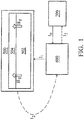
- FIG. 1 is a functional diagram of a portable electronic system showing the electrical energy transmission in accordance with some embodiments of the disclosure.
- FIG. 2 is a cross-sectional view of a semiconductor package assembly including a wire bond ball-grid-array (BGA) semiconductor package and a thermoelectric device chip integrated within in accordance with some embodiments of the disclosure.
- BGA ball-grid-array
- FIG. 1 is a functional diagram of a portable electronic system showing the electrical and thermal energies transmission in accordance with some embodiments of the disclosure.
- the portable electronic system comprises a semiconductor package assembly 500, a power system 600 and a battery 700.
- the semiconductor package assembly 500 comprises a semiconductor die 502 and a thermoelectric device chip 504 both packaged as a thermal energy recycling semiconductor package.
- the power system 600 is coupled to the semiconductor package assembly 500 and the battery 700.
- the battery 700 serves as a power source to output an electrical energy as a current I 0 and supply to the power system 600.
- the power system 600 is configured to distribute an electrical power as a current I 1 from the current I 0 to the semiconductor package assembly 500 for the operation of semiconductor die 502.
- the semiconductor die 502 generates a heat energy H T by the operation of the semiconductor die 502.
- the thermoelectric device chip 504 is configured to detect the heat energy H T generated from the semiconductor die 502 and to convert the heat energy H T into a recycled electrical energy and then output as a current I 2 to the power system 600.
- the power system 600 is also configured to store the recycled electrical energy as a stored recycled electrical energy and output as a current I 3 to charge the battery 700. Accordingly, the portable electronic system allows the heat energy generated from the semiconductor die 502 of the thermal energy recycling semiconductor package to be converted into a recycled electrical energy to be stored in the power system 600 and charge the battery 700.
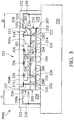
- FIG. 2 is a cross-sectional view of a semiconductor package assembly 500a.
- the semiconductor package assembly 500a includes a wire-bond ball-grid-array (BGA) semiconductor package 550a and a thermoelectric device chip 504 integrated within in accordance with some embodiments of the disclosure.
- the semiconductor package assembly 500a comprises a base 250, the wire-bond BGA semiconductor package 550a and a shielding case 232.
- the power system and the battery shown in FIG. 1 are not repeated for brevity.
- the base 250 for example a printed circuit board (PCB), may be formed of polypropylene (PP). It should also be noted that the base 250 can be a single layer or a multilayer structure.
- a plurality of conductive traces (not shown) and pads (not shown) is disposed on a device-attach surface 252 of the base 250.
- the conductive traces may comprise signal trace segments or ground trace segments, which are used for the input/output (I/O) connections of the BGA semiconductor package 550a.
- the pads are disposed on the device-attach surface 252, connecting to different terminals of the conductive traces. The pads are used for the wire-bond BGA semiconductor package 550a and the power system 600 as shown in FIG. 1 mounted directly thereon.
- the wire-bond BGA semiconductor package 550a is mounted on the device-attach surface 252 of the base 250 by a bonding process.
- the wire-bond BGA semiconductor package 550a is a package of large power consumption.
- the wire-bond BGA semiconductor package 550a may comprise a system-on-chip (SOC) package, a modem package, a radio-frequency (RF) module package including a power amplifier or a power management integrated circuit package.
- the SOC package may comprise a logic package.
- the wire-bond BGA semiconductor package 550a comprises a substrate 200, semiconductor dies 502a and 502b and a thermoelectric device chip 504a.
- the substrate 200 has a device-attach surface 201 and a bump-attach surface 203 opposite to the device-attach surface.
- the substrate 200 may comprise circuits 222, 224, 226, 228 and pads 202, 204, 206, 208, 222, 224, 226 and 228.
- the pads 202, 204, 206 and 208 are respectively disposed on the top of circuitries 222, 224, 226 and 228 close to the device-attach surface 201.
- the pads 222, 224, 226 and 228 are respectively disposed on the bottom of the circuitries 222, 224, 226 and 228 close to the bump-attach surface 203.
- the circuitries 222, 224, 226 and 228 of the wire-bond BGA semiconductor package 550a are interconnected with the circuitry of the base 200 via a plurality of conductive structures 240 disposed on the bump-attach surface 203 of the substrate 200. Also, the conductive structures 240 are in contact with the base 250.
- the conductive structures 240 may comprise a conductive bump structure such as a copper bump or a solder bump structure, a conductive pillar structure, a conductive wire structure, or a conductive paste structure.
- the semiconductor die 502a and 502b there are two semiconductor dies 502a and 502b attached to the substrate 200.
- the semiconductor die 502a is disposed on the device-attach surface 201 through an adhesion 501.
- the semiconductor die 502b is disposed on the semiconductor die 502a through an adhesion 503.
- the number of semiconductor dies is not limited to the disclosed embodiment.
- the semiconductor dies 502a and 502b may comprise a central processing unit (CPU), a graphics processing unit (GPU), a modem package, a power amplifier or a power management integrated circuit (PMIC) or any combination thereof.
- the semiconductor dies 502a and 502b are coupled to the pads 226 and 224 of the substrate 200 through bonding wires 508 and 506, respectively.
- thermoelectric device chip 504a is disposed over the semiconductor dies 502a and 502b, but separated from the semiconductor dies 502a and 502b through the molding compound 522. That is to say, the substrate 200 and the thermoelectric device chip 504a are disposed on opposite sides of the semiconductor dies 502a and 502b.
- the molding compound 522 covers the substrate 200 and surrounds the semiconductor dies 502a and 502b and thermoelectric device chip 504a, leaving a top surface 512 of the thermoelectric device chip 504a, a sidewall 230 and the bump-attach surface 203 of the substrate 200 exposed.
- the thermoelectric device chip 504a is arranged in a way that the top surface 512 is exposed to air, and the bottom surface 510 covered by the molding compound 522 is close to the semiconductor die 502b.
- the thermoelectric device chip 504a is configured to detect a heat energy (H T shown in FIG. 1 ) generated from the semiconductor dies 502a and 502b during operation.
- the heat energy results in a significant temperature difference between the top surface 512 and the bottom surface 510 of the thermoelectric device chip 504a. More specifically, the temperature of the bottom surface 510 is higher than that of the top surface 512 during operation of the semiconductor dies 502a and 502b.
- the thermoelectric device chip 504a can convert the detected temperature difference into an voltage difference between the top surface 512 and the bottom surface 510 of the thermoelectric device chip 504a.
- the thermoelectric device chip 504a comprises pads 514 and 516 coupled to the pads 222 and 228 of the substrate 200 by through mold vias (TMVs) 518 and 520 formed through the molding compound 522, respectively.
- the pads 514 and 516 are used to transmit an output current (I 2 shown in FIG. 1 ) translated from the voltage difference to the power system 600 as shown in FIG.
- thermoelectric device chip 504a senses the heat energy and converts into the current, the heat energy generated from the semiconductor dies 502a and 502b mainly dissipates through a path comprising the pads 204 and 206, the circuits 224 and 226 and the corresponding conductive structures 240.
- the shielding case 232 is disposed on the base 250.
- the shielding case 232 surrounds the wire-bond BGA semiconductor package 550a.
- the shielding case 232 has an opening 233 on the wire-bond BGA semiconductor package 550a, leaving the thermoelectric device chip 504a exposed by of the shielding case 232.
- An inner sidewall 234 of the shielding case 232 is spaced apart from a sidewall 524 of the wire-bond BGA semiconductor package 550a by a distance D.
- a space 238 surrounded by a sidewall 524 of the molding compound, the sidewall 230 of the substrate 200, the shielding case 232 and the base 250 is filled with air for the heat isolation function.
- the shielding case 232 may be formed by metal materials.
- an insulation film 236 may be conformably disposed on the inner sidewall 234 of the shielding case 232 for the improvement of the heat isolation function.
- FIG. 3 is a cross-sectional view of a semiconductor package assembly 500b including a flip-chip ball-grid-array (BGA) semiconductor package 550b and a thermoelectric device chip 504b integrated within in accordance with some embodiments of the disclosure. Elements of the embodiments hereinafter that are the same or similar as those previously described with reference to FIGS. 1 and 2 , are not repeated for brevity.
- the differences between the semiconductor package assembly 500a and semiconductor package assembly 500b comprise the flip-chip BGA semiconductor package 550b is fabricated using the flip-chip technology. Accordingly, a semiconductor die 502c of the flip-chip BGA semiconductor package 550b may be designed to be in contact with a thermoelectric device chip 504b packaged within.
- the flip-chip BGA semiconductor package 550b is a package of large power consumption with a function similar to the wire-bond BGA semiconductor package 550a.
- the flip-chip BGA semiconductor package 550b comprises at least one semiconductor die 502c turned upside down and mounted on the substrate 200 using the flip-chip technology. More specifically, the semiconductor die 502c has a top surface 507 and a bottom surface 505. The top surface 507 of the semiconductor die 502c is coupled to the pad 226 of the substrate 200 using solder balls 530 disposed thereon. The bottom surface 505 of the semiconductor die 502c is coupled to the thermoelectric device chip 504b using pads 528 disposed on. In this embodiment, the pads 528 of the semiconductor die 502c is in contact with corresponding pads 526 of the thermoelectric device chip 504b.
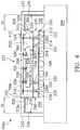
- FIG. 4 is a cross-sectional view of a semiconductor package assembly including a flip-chip ball-grid-array (BGA) semiconductor package 550c and a thermoelectric device chip 504c integrated within in accordance with some embodiments of the disclosure. Elements of the embodiments hereinafter that are the same or similar as those previously described with reference to FIGS. 1-3 , are not repeated for brevity.
- the semiconductor package assembly 500c and semiconductor package assembly 500b is that the semiconductor package assembly 500c comprises a semiconductor die 502c of the flip-chip BGA semiconductor package 550c may be designed to be separated from a thermoelectric device chip 504b packaged within.
- the flip-chip BGA semiconductor package 550c is a package of large power consumption with a function similar to the flip-chip BGA semiconductor package 550b.
- the semiconductor die 502c of the flip-chip BGA semiconductor package 550c has a top surface 507 and a bottom surface 505.
- the top surface 507 of the semiconductor die 502c is coupled to the pad 226 of the substrate 200 using solder balls 530 disposed thereon.
- the bottom surface 505 of the semiconductor die 502c is coupled to the thermoelectric device chip 504b using pads 528 disposed on.
- the pads 528 of the semiconductor die 502c is separated from corresponding pads 526 of the thermoelectric device chip 504c by conductive bumps 530.
- the pads 528 of the semiconductor die 502c and the pads 526 of the thermoelectric device chip 504c are in contact with the corresponding conductive bumps 530.
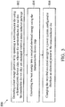
- FIG. 5 is a flow chart showing a method 800 for converting a thermal energy into an electrical energy in a portable electronic system as shown in FIG. 1 .
- the thermoelectric device chip 504 is used to detect a heat energy H T generated by operating a semiconductor die 502.
- the semiconductor die 502 and the thermoelectric device chip 504 are packaged within a semiconductor package, for example, the wire-bond BGA semiconductor package 550a and the flip-chip BGA semiconductor packages 550b-550c as shown in FIGS. 2-4 .
- FIGS. 1 the thermoelectric device chip 504 is used to detect a heat energy H T generated by operating a semiconductor die 502.
- the semiconductor die 502 and the thermoelectric device chip 504 are packaged within a semiconductor package, for example, the wire-bond BGA semiconductor package 550a and the flip-chip BGA semiconductor packages 550b-550c as shown in FIGS. 2-4 .
- each of the thermoelectric device chips 504a-504c has the bottom surface 510 close to the semiconductor die 502b-502c and the top surface 512 opposite to the bottom surface 510.
- Each of the thermoelectric device chips 504a-504c is arranged in such a way that the top surface 512 is exposed to air, and the bottom surface 510 is covered by the molding compound 522.
- the temperature of the bottom surface 510 is higher than that of the top surface 512 while operating the semiconductor dies 500a-500c (step 802).
- step 804 the heat energy H T is converted into a recycled electrical energy using the thermoelectric device chip 504 and then output as the current I 2 as shown in FIG. 1 .
- step 806 the recycled electrical energy (as the current I 2 ) is charged to a power system 600 as shown in FIG. 1 .
- the power system 600 is configured to distribute an electrical power to the semiconductor die 500 as shown in FIG. 1 .
- the step 806 further includes transmitting the recycled electrical energy to a charger of the power system 600 as shown in FIG. 1 , so that the charger stored the recycled electrical energy as a stored recycled electrical energy.
- the step 806 further includes translating the stored recycled electrical energy into the current I 2 to charge the battery 700 after transmitting the recycled electrical energy to a charger of the power system 600 as shown in FIG. 1 .
- Embodiments provide a portable electronic system with the thermal recycling function.
- the portable electronic system includes a thermal energy recycling semiconductor package having at least one semiconductor die with large power consumption and a thermoelectric device chip disposed close thereto.
- the portable electronic system allows the heat energy generated from the semiconductor die of the thermal energy recycling semiconductor package to be converted into a recycled electrical energy to be stored in the power system and charge the battery. Accordingly, the heat energy generated from the semiconductor die can be recycled to an electrical energy to provide to the portable electronic system.
Landscapes
- Engineering & Computer Science (AREA)
- Power Engineering (AREA)
- Microelectronics & Electronic Packaging (AREA)
- Computer Hardware Design (AREA)
- Physics & Mathematics (AREA)
- Condensed Matter Physics & Semiconductors (AREA)
- General Physics & Mathematics (AREA)
- Manufacturing & Machinery (AREA)
- Cooling Or The Like Of Semiconductors Or Solid State Devices (AREA)
- Automation & Control Theory (AREA)
- Structures Or Materials For Encapsulating Or Coating Semiconductor Devices Or Solid State Devices (AREA)
- Wire Bonding (AREA)
Claims (13)
- Tragbares elektronisches System, umfassend:
ein Halbleiterpaket (550a-550c), umfassend:ein Substrat (200);ein Halbleiter-Die (502, 502a-502c), das mit dem Substrat gekoppelt ist; undeinen Thermoelektrische-Vorrichtungs-Chip (504, 504a-504c), der nahe dem mit dem Substrat gekoppelten Halbleiter-Die angeordnet und konfiguriert ist, eine Wärmeenergie (HT) zu detektieren, die von dem Halbleiter-Die erzeugt wird, und die Wärmeenergie in eine recycelte elektrische Energie umzuwandeln; und ein Stromversorgungssystem (power system) (600), das mit dem Halbleiterpaket gekoppelt und konfiguriert ist, die recycelte elektrische Energie zu speichern;wobei das Substrat (200) und der Thermoelektrische-Vorrichtungs-Chip (504, 504a-504c) auf gegenüberliegenden Seiten des Halbleiter-Die (502, 502a-502c) angeordnet sind. - Tragbares elektronisches System nach Anspruch 1, ferner umfassend eine Batterie (700), die mit dem Stromversorgungssystem gekoppelt und konfiguriert ist, eine elektrische Energie an das Stromversorgungssystem zu liefern und mit einer gespeicherten recycelten elektrischen Energie von dem Stromversorgungssystem geladen zu werden.
- Tragbares elektronisches System nach Anspruch 1 oder 2, ferner umfassend eine Basis (250), wobei das Halbleiterpaket auf der Basis angebracht ist.
- Tragbares elektronisches System nach Anspruch 3, ferner umfassend ein Abschirmgehäuse (232), das auf der Basis angeordnet ist und das Halbleiterpaket umgibt, und wobei der Thermoelektrische-Vorrichtungs-Chip durch eine Öffnung (233) des Abschirmgehäuses freigelegt ist.
- Tragbares elektronisches System nach Anspruch 4, wobei eine innere Seitenwand (234) des Abschirmgehäuses von einer Seitenwand (524) des Halbleiterpakets um einen Abstand (D) beabstandet ist.
- Tragbares elektronisches System nach Anspruch 5, wobei ein Raum (238), der von der Seitenwand des Halbleiterpakets, dem Abschirmgehäuse und der Basis umgeben ist, mit Luft gefüllt ist.
- Tragbares elektronisches System nach Anspruch 5 oder 6, ferner umfassend einen Isolierungsfilm (236), der an der inneren Seitenwand des Abschirmgehäuses angeordnet ist.
- Tragbares elektronisches System nach einem der vorstehenden Ansprüche, wobei das Halbleiter-Die (502c) eine obere Fläche (507) und eine untere Fläche (505) aufweist, das Halbleiter-Die mit dem Substrat unter Verwendung von Lötkugeln (530) gekoppelt ist, die auf der oberen Fläche angeordnet sind, und das Halbleiter-Die mit dem Thermoelektrische-Vorrichtungs-Chip unter Verwendung von Pads (528) gekoppelt ist, die an der unteren Fläche angeordnet sind.
- Tragbares elektronisches System nach Anspruch 4,
wobei der Thermoelektrische-Vorrichtungs-Chip (504, 504a-504c) auf das Halbleiter-Die geschichtet ist, wobei das Abschirmgehäuse eine obere Fläche des Thermoelektrische-Vorrichtungs-Chips nicht abdeckt; und
wobei das Stromversorgungssystem (600) auf der Basis angebracht ist. - Tragbares elektronische System nach Anspruch 9, ferner umfassend eine Formmasse (522), die das Substrat abdeckt und das Halbleiter-Die und den Thermoelektrische-Vorrichtungs-Chip umgibt, was die obere Fläche (512) des Thermoelektrische-Vorrichtungs-Chips, eine Seitenwand (230) und eine untere Fläche (203) des Substrats freigelegt lässt.
- Verfahren (800) zum Umwandeln einer Wärmeenergie in eine elektrische Energie in einem tragbaren elektronischen System, wobei das tragbare elektronische System folgendes umfasst:
ein Halbleiterpaket (550a-550c), umfassend:ein Substrat (200);ein Halbleiter-Die (502, 502a-502c), das mit dem Substrat gekoppelt ist; undeinen Thermoelektrische-Vorrichtungs-Chip (504, 504a-504c), der nahe dem mit dem Substrat gekoppelten Halbleiter-Die angeordnet und konfiguriert ist, eine Wärmeenergie (HT) zu detektieren, die von dem Halbleiter-Die erzeugt wird, und die Wärmeenergie in eine recycelte elektrische Energie umzuwandeln; undein Stromversorgungssystem (power system) (600), das mit dem Halbleiterpaket gekoppelt und konfiguriert ist, die recycelte elektrische Energie zu speichern;wobei das Substrat (200) und der Thermoelektrische-Vorrichtungs-Chip (504, 504a-504c) auf gegenüberliegenden Seiten des Halbleiter-Die (502, 502a-502c) angeordnet sind;wobei das Verfahren folgendes umfasst:Detektieren einer Wärmeenergie, die durch Betreiben des Halbleiter-Die erzeugt wird, unter Verwendung des Thermoelektrische-Vorrichtungs-Chips, wobei das Halbleiter-Die und der Thermoelektrische-Vorrichtungs-Chip in das Halbleiterpaket (802) gepackt sind;Umwandeln der Wärmeenergie in eine recycelte elektrische Energie unter Verwendung des Thermoelektrische-Vorrichtungs-Chips (804); undLaden der recycelten elektrischen Energie in das Stromversorgungssystem, das konfiguriert ist, elektrische Leistung an das Halbleiter-Die (806) zu verteilen. - Verfahren nach Anspruch 11, wobei das Laden der recycelten elektrischen Energie in das Stromversorgungssystem ferner umfasst:
Übertragen der recycelten elektrischen Energie in eine Ladevorrichtung des Stromversorgungssystems (600), sodass die Ladevorrichtung die recycelte elektrische Energie als eine gespeicherte recycelte elektrische Energie speichert. - Verfahren nach Anspruch 11 oder 12, wobei der Thermoelektrische-Vorrichtungs-Chip eine erste Fläche (510) nahe des Halbleiter-Die und eine zweite Fläche (512) gegenüber der ersten Fläche aufweist, wobei eine Temperatur der ersten Fläche während des Betriebs des Halbleiter-Die höher ist als die der zweiten Fläche.
Applications Claiming Priority (1)
| Application Number | Priority Date | Filing Date | Title |
|---|---|---|---|
| US14/717,159 US9837595B2 (en) | 2015-05-20 | 2015-05-20 | Semiconductor package assembly with thermal recycling function |
Publications (3)
| Publication Number | Publication Date |
|---|---|
| EP3096366A2 EP3096366A2 (de) | 2016-11-23 |
| EP3096366A3 EP3096366A3 (de) | 2016-12-28 |
| EP3096366B1 true EP3096366B1 (de) | 2019-05-01 |
Family
ID=53487256
Family Applications (1)
| Application Number | Title | Priority Date | Filing Date |
|---|---|---|---|
| EP15173493.6A Active EP3096366B1 (de) | 2015-05-20 | 2015-06-24 | Halbleiterverpackungsanordnung mit thermischer recyclingfunktion |
Country Status (3)
| Country | Link |
|---|---|
| US (1) | US9837595B2 (de) |
| EP (1) | EP3096366B1 (de) |
| CN (1) | CN106169451B (de) |
Cited By (1)
| Publication number | Priority date | Publication date | Assignee | Title |
|---|---|---|---|---|
| US11705756B2 (en) | 2020-04-22 | 2023-07-18 | Board Of Trustees Of The University Of Arkansas | Device for ambient thermal and vibration energy harvesting |
Families Citing this family (12)
| Publication number | Priority date | Publication date | Assignee | Title |
|---|---|---|---|---|
| WO2015014563A1 (en) * | 2013-07-30 | 2015-02-05 | Harman Becker Automotive Systems Gmbh | Electronic module |
| US10665579B2 (en) * | 2016-02-16 | 2020-05-26 | Xilinx, Inc. | Chip package assembly with power management integrated circuit and integrated circuit die |
| US10600948B1 (en) * | 2016-11-28 | 2020-03-24 | Intel Corporation | Package with thermoelectric power feedback loop |
| US10504816B2 (en) | 2017-09-06 | 2019-12-10 | Google Llc | Thermoelectric cooler (TEC) for spot cooling of 2.5D/3D IC packages |
| AU2019278835B2 (en) | 2018-05-30 | 2025-04-24 | Board Of Trustees Of The University Of Arkansas | Energy harvesting devices and sensors, and methods of making and use thereof |
| US11784108B2 (en) | 2019-08-06 | 2023-10-10 | Intel Corporation | Thermal management in integrated circuit packages |
| US20210043543A1 (en) * | 2019-08-06 | 2021-02-11 | Intel Corporation | Thermal management in integrated circuit packages |
| US12007170B2 (en) | 2019-08-06 | 2024-06-11 | Intel Corporation | Thermal management in integrated circuit packages |
| US11830787B2 (en) | 2019-08-06 | 2023-11-28 | Intel Corporation | Thermal management in integrated circuit packages |
| KR102835611B1 (ko) * | 2020-05-08 | 2025-07-16 | 삼성전자주식회사 | 반도체 패키지 및 이를 포함한 전자 장치 |
| CN112333978B (zh) * | 2020-10-19 | 2023-06-06 | Oppo广东移动通信有限公司 | 散热组件及电子设备、散热控制方法 |
| US12302769B2 (en) * | 2023-06-08 | 2025-05-13 | Limitless Space Institute | Casimir power cell |
Family Cites Families (8)
| Publication number | Priority date | Publication date | Assignee | Title |
|---|---|---|---|---|
| JP3219055B2 (ja) | 1998-06-26 | 2001-10-15 | 日本電気株式会社 | 電子装置 |
| GB2495126B (en) | 2009-04-15 | 2015-03-18 | Hewlett Packard Development Co | Generating and using electricity derived from waste heat of an electrical appliance |
| CN101931347B (zh) * | 2010-07-23 | 2014-07-30 | 惠州Tcl移动通信有限公司 | 提升能耗效率的方法及其移动终端和热电转换模块的用途 |
| JP5564455B2 (ja) | 2011-03-17 | 2014-07-30 | 富士フイルム株式会社 | 熱電発電装置及び携帯型電子機器 |
| US20140176041A1 (en) * | 2012-12-20 | 2014-06-26 | Nvidia Corporation | Semiconductor thermoelectric module charger for mobile computing device |
| US20140252531A1 (en) * | 2013-03-07 | 2014-09-11 | Qualcomm Incorporated | Systems and methods for harvesting dissipated heat from integrated circuits (ics) in electronic devices into electrical energy for providing power for the electronic devices |
| DE102013222163A1 (de) | 2013-10-31 | 2015-05-21 | Robert Bosch Gmbh | Elektrische Schaltung und Verfahren zur Herstellung einer elektrischen Schaltung |
| US9491865B1 (en) * | 2015-04-24 | 2016-11-08 | Unimicron Technology Corp. | Circuit board and method for manufacturing the same |
-
2015
- 2015-05-20 US US14/717,159 patent/US9837595B2/en active Active
- 2015-06-24 EP EP15173493.6A patent/EP3096366B1/de active Active
-
2016
- 2016-05-19 CN CN201610332811.0A patent/CN106169451B/zh active Active
Non-Patent Citations (1)
| Title |
|---|
| None * |
Cited By (2)
| Publication number | Priority date | Publication date | Assignee | Title |
|---|---|---|---|---|
| US11705756B2 (en) | 2020-04-22 | 2023-07-18 | Board Of Trustees Of The University Of Arkansas | Device for ambient thermal and vibration energy harvesting |
| US12381418B2 (en) | 2020-04-22 | 2025-08-05 | Board Of Trustees Of The University Of Arkansas | Device for ambient thermal and vibration energy harvesting |
Also Published As
| Publication number | Publication date |
|---|---|
| CN106169451A (zh) | 2016-11-30 |
| US20160343929A1 (en) | 2016-11-24 |
| CN106169451B (zh) | 2019-01-22 |
| EP3096366A2 (de) | 2016-11-23 |
| EP3096366A3 (de) | 2016-12-28 |
| US9837595B2 (en) | 2017-12-05 |
Similar Documents
| Publication | Publication Date | Title |
|---|---|---|
| EP3096366B1 (de) | Halbleiterverpackungsanordnung mit thermischer recyclingfunktion | |
| US11728292B2 (en) | Semiconductor package assembly having a conductive electromagnetic shield layer | |
| US11658090B2 (en) | Semiconductor package system | |
| US12406899B2 (en) | Semiconductor package system | |
| EP3007225B1 (de) | Halbleitergehäuseanordnung | |
| US20140133105A1 (en) | Method of embedding cpu/gpu/logic chip into a substrate of a package-on-package structure | |
| US20160005675A1 (en) | Double sided cooling chip package and method of manufacturing the same | |
| US10950554B2 (en) | Semiconductor packages with electromagnetic interference shielding layer and methods of forming the same | |
| EP3091573A2 (de) | Halbleiter-chippackungsanordnung mit verbesserter wärmeableitungsleistung | |
| CN108269797A (zh) | 电子装置封装 | |
| CN101594730B (zh) | 具有导热结构的电路板 | |
| US11600607B2 (en) | Semiconductor module including multiple power management semiconductor packages | |
| KR20120019091A (ko) | 멀티-칩 패키지 및 그의 제조 방법 | |
| KR20140113029A (ko) | 열전소자가 배치된 히트 슬러그 및 이를 구비하는 반도체 패키지 | |
| US9390992B2 (en) | Semiconductor packages including a metal layer between first and second semiconductor chips | |
| US20080093733A1 (en) | Chip package and manufacturing method thereof | |
| US10582617B2 (en) | Method of fabricating a circuit module | |
| US8288847B2 (en) | Dual die semiconductor package | |
| US20240379534A1 (en) | Electronic package, manufacturing method for the same, and electronic structure | |
| US20120168936A1 (en) | Multi-chip stack package structure and fabrication method thereof | |
| KR20190130444A (ko) | 반도체 패키지 시스템 | |
| CN115939060A (zh) | 包含直接接触热路径的设备及其制造方法 | |
| KR20200073643A (ko) | 반도체 패키지 및 반도체 패키지의 제조 방법 | |
| KR20090080879A (ko) | 웨이퍼 레벨 칩 스케일 패키지 및 그의 제조 방법 | |
| CN104218034A (zh) | 半导体封装 |
Legal Events
| Date | Code | Title | Description |
|---|---|---|---|
| PUAI | Public reference made under article 153(3) epc to a published international application that has entered the european phase |
Free format text: ORIGINAL CODE: 0009012 |
|
| AK | Designated contracting states |
Kind code of ref document: A2 Designated state(s): AL AT BE BG CH CY CZ DE DK EE ES FI FR GB GR HR HU IE IS IT LI LT LU LV MC MK MT NL NO PL PT RO RS SE SI SK SM TR |
|
| AX | Request for extension of the european patent |
Extension state: BA ME |
|
| PUAL | Search report despatched |
Free format text: ORIGINAL CODE: 0009013 |
|
| AK | Designated contracting states |
Kind code of ref document: A3 Designated state(s): AL AT BE BG CH CY CZ DE DK EE ES FI FR GB GR HR HU IE IS IT LI LT LU LV MC MK MT NL NO PL PT RO RS SE SI SK SM TR |
|
| AX | Request for extension of the european patent |
Extension state: BA ME |
|
| RIC1 | Information provided on ipc code assigned before grant |
Ipc: H01L 23/38 20060101ALI20161118BHEP Ipc: H01L 35/28 20060101AFI20161118BHEP |
|
| STAA | Information on the status of an ep patent application or granted ep patent |
Free format text: STATUS: REQUEST FOR EXAMINATION WAS MADE |
|
| 17P | Request for examination filed |
Effective date: 20170628 |
|
| RBV | Designated contracting states (corrected) |
Designated state(s): AL AT BE BG CH CY CZ DE DK EE ES FI FR GB GR HR HU IE IS IT LI LT LU LV MC MK MT NL NO PL PT RO RS SE SI SK SM TR |
|
| GRAP | Despatch of communication of intention to grant a patent |
Free format text: ORIGINAL CODE: EPIDOSNIGR1 |
|
| STAA | Information on the status of an ep patent application or granted ep patent |
Free format text: STATUS: GRANT OF PATENT IS INTENDED |
|
| INTG | Intention to grant announced |
Effective date: 20181212 |
|
| GRAS | Grant fee paid |
Free format text: ORIGINAL CODE: EPIDOSNIGR3 |
|
| GRAA | (expected) grant |
Free format text: ORIGINAL CODE: 0009210 |
|
| STAA | Information on the status of an ep patent application or granted ep patent |
Free format text: STATUS: THE PATENT HAS BEEN GRANTED |
|
| AK | Designated contracting states |
Kind code of ref document: B1 Designated state(s): AL AT BE BG CH CY CZ DE DK EE ES FI FR GB GR HR HU IE IS IT LI LT LU LV MC MK MT NL NO PL PT RO RS SE SI SK SM TR |
|
| REG | Reference to a national code |
Ref country code: GB Ref legal event code: FG4D |
|
| REG | Reference to a national code |
Ref country code: CH Ref legal event code: EP Ref country code: AT Ref legal event code: REF Ref document number: 1128103 Country of ref document: AT Kind code of ref document: T Effective date: 20190515 |
|
| REG | Reference to a national code |
Ref country code: DE Ref legal event code: R096 Ref document number: 602015029174 Country of ref document: DE |
|
| REG | Reference to a national code |
Ref country code: IE Ref legal event code: FG4D |
|
| REG | Reference to a national code |
Ref country code: NL Ref legal event code: MP Effective date: 20190501 |
|
| REG | Reference to a national code |
Ref country code: LT Ref legal event code: MG4D |
|
| PG25 | Lapsed in a contracting state [announced via postgrant information from national office to epo] |
Ref country code: FI Free format text: LAPSE BECAUSE OF FAILURE TO SUBMIT A TRANSLATION OF THE DESCRIPTION OR TO PAY THE FEE WITHIN THE PRESCRIBED TIME-LIMIT Effective date: 20190501 Ref country code: AL Free format text: LAPSE BECAUSE OF FAILURE TO SUBMIT A TRANSLATION OF THE DESCRIPTION OR TO PAY THE FEE WITHIN THE PRESCRIBED TIME-LIMIT Effective date: 20190501 Ref country code: NO Free format text: LAPSE BECAUSE OF FAILURE TO SUBMIT A TRANSLATION OF THE DESCRIPTION OR TO PAY THE FEE WITHIN THE PRESCRIBED TIME-LIMIT Effective date: 20190801 Ref country code: ES Free format text: LAPSE BECAUSE OF FAILURE TO SUBMIT A TRANSLATION OF THE DESCRIPTION OR TO PAY THE FEE WITHIN THE PRESCRIBED TIME-LIMIT Effective date: 20190501 Ref country code: HR Free format text: LAPSE BECAUSE OF FAILURE TO SUBMIT A TRANSLATION OF THE DESCRIPTION OR TO PAY THE FEE WITHIN THE PRESCRIBED TIME-LIMIT Effective date: 20190501 Ref country code: SE Free format text: LAPSE BECAUSE OF FAILURE TO SUBMIT A TRANSLATION OF THE DESCRIPTION OR TO PAY THE FEE WITHIN THE PRESCRIBED TIME-LIMIT Effective date: 20190501 Ref country code: LT Free format text: LAPSE BECAUSE OF FAILURE TO SUBMIT A TRANSLATION OF THE DESCRIPTION OR TO PAY THE FEE WITHIN THE PRESCRIBED TIME-LIMIT Effective date: 20190501 Ref country code: PT Free format text: LAPSE BECAUSE OF FAILURE TO SUBMIT A TRANSLATION OF THE DESCRIPTION OR TO PAY THE FEE WITHIN THE PRESCRIBED TIME-LIMIT Effective date: 20190901 Ref country code: NL Free format text: LAPSE BECAUSE OF FAILURE TO SUBMIT A TRANSLATION OF THE DESCRIPTION OR TO PAY THE FEE WITHIN THE PRESCRIBED TIME-LIMIT Effective date: 20190501 |
|
| PG25 | Lapsed in a contracting state [announced via postgrant information from national office to epo] |
Ref country code: RS Free format text: LAPSE BECAUSE OF FAILURE TO SUBMIT A TRANSLATION OF THE DESCRIPTION OR TO PAY THE FEE WITHIN THE PRESCRIBED TIME-LIMIT Effective date: 20190501 Ref country code: LV Free format text: LAPSE BECAUSE OF FAILURE TO SUBMIT A TRANSLATION OF THE DESCRIPTION OR TO PAY THE FEE WITHIN THE PRESCRIBED TIME-LIMIT Effective date: 20190501 Ref country code: GR Free format text: LAPSE BECAUSE OF FAILURE TO SUBMIT A TRANSLATION OF THE DESCRIPTION OR TO PAY THE FEE WITHIN THE PRESCRIBED TIME-LIMIT Effective date: 20190802 Ref country code: BG Free format text: LAPSE BECAUSE OF FAILURE TO SUBMIT A TRANSLATION OF THE DESCRIPTION OR TO PAY THE FEE WITHIN THE PRESCRIBED TIME-LIMIT Effective date: 20190801 |
|
| REG | Reference to a national code |
Ref country code: AT Ref legal event code: MK05 Ref document number: 1128103 Country of ref document: AT Kind code of ref document: T Effective date: 20190501 |
|
| PG25 | Lapsed in a contracting state [announced via postgrant information from national office to epo] |
Ref country code: IS Free format text: LAPSE BECAUSE OF FAILURE TO SUBMIT A TRANSLATION OF THE DESCRIPTION OR TO PAY THE FEE WITHIN THE PRESCRIBED TIME-LIMIT Effective date: 20190901 |
|
| PG25 | Lapsed in a contracting state [announced via postgrant information from national office to epo] |
Ref country code: CZ Free format text: LAPSE BECAUSE OF FAILURE TO SUBMIT A TRANSLATION OF THE DESCRIPTION OR TO PAY THE FEE WITHIN THE PRESCRIBED TIME-LIMIT Effective date: 20190501 Ref country code: MC Free format text: LAPSE BECAUSE OF FAILURE TO SUBMIT A TRANSLATION OF THE DESCRIPTION OR TO PAY THE FEE WITHIN THE PRESCRIBED TIME-LIMIT Effective date: 20190501 Ref country code: SK Free format text: LAPSE BECAUSE OF FAILURE TO SUBMIT A TRANSLATION OF THE DESCRIPTION OR TO PAY THE FEE WITHIN THE PRESCRIBED TIME-LIMIT Effective date: 20190501 Ref country code: AT Free format text: LAPSE BECAUSE OF FAILURE TO SUBMIT A TRANSLATION OF THE DESCRIPTION OR TO PAY THE FEE WITHIN THE PRESCRIBED TIME-LIMIT Effective date: 20190501 Ref country code: EE Free format text: LAPSE BECAUSE OF FAILURE TO SUBMIT A TRANSLATION OF THE DESCRIPTION OR TO PAY THE FEE WITHIN THE PRESCRIBED TIME-LIMIT Effective date: 20190501 Ref country code: DK Free format text: LAPSE BECAUSE OF FAILURE TO SUBMIT A TRANSLATION OF THE DESCRIPTION OR TO PAY THE FEE WITHIN THE PRESCRIBED TIME-LIMIT Effective date: 20190501 Ref country code: RO Free format text: LAPSE BECAUSE OF FAILURE TO SUBMIT A TRANSLATION OF THE DESCRIPTION OR TO PAY THE FEE WITHIN THE PRESCRIBED TIME-LIMIT Effective date: 20190501 |
|
| REG | Reference to a national code |
Ref country code: CH Ref legal event code: PL |
|
| REG | Reference to a national code |
Ref country code: DE Ref legal event code: R097 Ref document number: 602015029174 Country of ref document: DE |
|
| PG25 | Lapsed in a contracting state [announced via postgrant information from national office to epo] |
Ref country code: SM Free format text: LAPSE BECAUSE OF FAILURE TO SUBMIT A TRANSLATION OF THE DESCRIPTION OR TO PAY THE FEE WITHIN THE PRESCRIBED TIME-LIMIT Effective date: 20190501 Ref country code: IT Free format text: LAPSE BECAUSE OF FAILURE TO SUBMIT A TRANSLATION OF THE DESCRIPTION OR TO PAY THE FEE WITHIN THE PRESCRIBED TIME-LIMIT Effective date: 20190501 |
|
| PLBE | No opposition filed within time limit |
Free format text: ORIGINAL CODE: 0009261 |
|
| STAA | Information on the status of an ep patent application or granted ep patent |
Free format text: STATUS: NO OPPOSITION FILED WITHIN TIME LIMIT |
|
| REG | Reference to a national code |
Ref country code: BE Ref legal event code: MM Effective date: 20190630 |
|
| PG25 | Lapsed in a contracting state [announced via postgrant information from national office to epo] |
Ref country code: TR Free format text: LAPSE BECAUSE OF FAILURE TO SUBMIT A TRANSLATION OF THE DESCRIPTION OR TO PAY THE FEE WITHIN THE PRESCRIBED TIME-LIMIT Effective date: 20190501 |
|
| 26N | No opposition filed |
Effective date: 20200204 |
|
| PG25 | Lapsed in a contracting state [announced via postgrant information from national office to epo] |
Ref country code: PL Free format text: LAPSE BECAUSE OF FAILURE TO SUBMIT A TRANSLATION OF THE DESCRIPTION OR TO PAY THE FEE WITHIN THE PRESCRIBED TIME-LIMIT Effective date: 20190501 Ref country code: IE Free format text: LAPSE BECAUSE OF NON-PAYMENT OF DUE FEES Effective date: 20190624 |
|
| PG25 | Lapsed in a contracting state [announced via postgrant information from national office to epo] |
Ref country code: SI Free format text: LAPSE BECAUSE OF FAILURE TO SUBMIT A TRANSLATION OF THE DESCRIPTION OR TO PAY THE FEE WITHIN THE PRESCRIBED TIME-LIMIT Effective date: 20190501 Ref country code: LI Free format text: LAPSE BECAUSE OF NON-PAYMENT OF DUE FEES Effective date: 20190630 Ref country code: CH Free format text: LAPSE BECAUSE OF NON-PAYMENT OF DUE FEES Effective date: 20190630 Ref country code: LU Free format text: LAPSE BECAUSE OF NON-PAYMENT OF DUE FEES Effective date: 20190624 Ref country code: BE Free format text: LAPSE BECAUSE OF NON-PAYMENT OF DUE FEES Effective date: 20190630 |
|
| PG25 | Lapsed in a contracting state [announced via postgrant information from national office to epo] |
Ref country code: CY Free format text: LAPSE BECAUSE OF FAILURE TO SUBMIT A TRANSLATION OF THE DESCRIPTION OR TO PAY THE FEE WITHIN THE PRESCRIBED TIME-LIMIT Effective date: 20190501 |
|
| PG25 | Lapsed in a contracting state [announced via postgrant information from national office to epo] |
Ref country code: MT Free format text: LAPSE BECAUSE OF FAILURE TO SUBMIT A TRANSLATION OF THE DESCRIPTION OR TO PAY THE FEE WITHIN THE PRESCRIBED TIME-LIMIT Effective date: 20190501 Ref country code: HU Free format text: LAPSE BECAUSE OF FAILURE TO SUBMIT A TRANSLATION OF THE DESCRIPTION OR TO PAY THE FEE WITHIN THE PRESCRIBED TIME-LIMIT; INVALID AB INITIO Effective date: 20150624 |
|
| PG25 | Lapsed in a contracting state [announced via postgrant information from national office to epo] |
Ref country code: MK Free format text: LAPSE BECAUSE OF FAILURE TO SUBMIT A TRANSLATION OF THE DESCRIPTION OR TO PAY THE FEE WITHIN THE PRESCRIBED TIME-LIMIT Effective date: 20190501 |
|
| REG | Reference to a national code |
Ref country code: DE Ref legal event code: R079 Ref document number: 602015029174 Country of ref document: DE Free format text: PREVIOUS MAIN CLASS: H01L0035280000 Ipc: H10N0010100000 |
|
| P01 | Opt-out of the competence of the unified patent court (upc) registered |
Effective date: 20230607 |
|
| PGFP | Annual fee paid to national office [announced via postgrant information from national office to epo] |
Ref country code: DE Payment date: 20250429 Year of fee payment: 11 |
|
| PGFP | Annual fee paid to national office [announced via postgrant information from national office to epo] |
Ref country code: GB Payment date: 20250501 Year of fee payment: 11 |
|
| PGFP | Annual fee paid to national office [announced via postgrant information from national office to epo] |
Ref country code: FR Payment date: 20250508 Year of fee payment: 11 |