EP3096353A1 - Rf amplifier output circuit device with integrated current path, and methods of manufacture thereof - Google Patents
Rf amplifier output circuit device with integrated current path, and methods of manufacture thereof Download PDFInfo
- Publication number
- EP3096353A1 EP3096353A1 EP16169901.2A EP16169901A EP3096353A1 EP 3096353 A1 EP3096353 A1 EP 3096353A1 EP 16169901 A EP16169901 A EP 16169901A EP 3096353 A1 EP3096353 A1 EP 3096353A1
- Authority
- EP
- European Patent Office
- Prior art keywords
- ceramic
- electrode
- conductor
- capacitor
- coupled
- Prior art date
- Legal status (The legal status is an assumption and is not a legal conclusion. Google has not performed a legal analysis and makes no representation as to the accuracy of the status listed.)
- Granted
Links
Images


Classifications
-
- H—ELECTRICITY
- H03—ELECTRONIC CIRCUITRY
- H03F—AMPLIFIERS
- H03F1/00—Details of amplifiers with only discharge tubes, only semiconductor devices or only unspecified devices as amplifying elements
- H03F1/56—Modifications of input or output impedances, not otherwise provided for
- H03F1/565—Modifications of input or output impedances, not otherwise provided for using inductive elements
-
- H—ELECTRICITY
- H03—ELECTRONIC CIRCUITRY
- H03F—AMPLIFIERS
- H03F1/00—Details of amplifiers with only discharge tubes, only semiconductor devices or only unspecified devices as amplifying elements
- H03F1/56—Modifications of input or output impedances, not otherwise provided for
-
- H—ELECTRICITY
- H01—ELECTRIC ELEMENTS
- H01F—MAGNETS; INDUCTANCES; TRANSFORMERS; SELECTION OF MATERIALS FOR THEIR MAGNETIC PROPERTIES
- H01F27/00—Details of transformers or inductances, in general
- H01F27/28—Coils; Windings; Conductive connections
- H01F27/2804—Printed windings
-
- H—ELECTRICITY
- H01—ELECTRIC ELEMENTS
- H01G—CAPACITORS; CAPACITORS, RECTIFIERS, DETECTORS, SWITCHING DEVICES OR LIGHT-SENSITIVE DEVICES, OF THE ELECTROLYTIC TYPE
- H01G4/00—Fixed capacitors; Processes of their manufacture
- H01G4/002—Details
- H01G4/005—Electrodes
-
- H—ELECTRICITY
- H01—ELECTRIC ELEMENTS
- H01G—CAPACITORS; CAPACITORS, RECTIFIERS, DETECTORS, SWITCHING DEVICES OR LIGHT-SENSITIVE DEVICES, OF THE ELECTROLYTIC TYPE
- H01G4/00—Fixed capacitors; Processes of their manufacture
- H01G4/002—Details
- H01G4/018—Dielectrics
- H01G4/06—Solid dielectrics
- H01G4/08—Inorganic dielectrics
- H01G4/12—Ceramic dielectrics
-
- H—ELECTRICITY
- H01—ELECTRIC ELEMENTS
- H01G—CAPACITORS; CAPACITORS, RECTIFIERS, DETECTORS, SWITCHING DEVICES OR LIGHT-SENSITIVE DEVICES, OF THE ELECTROLYTIC TYPE
- H01G4/00—Fixed capacitors; Processes of their manufacture
- H01G4/30—Stacked capacitors
-
- H—ELECTRICITY
- H01—ELECTRIC ELEMENTS
- H01G—CAPACITORS; CAPACITORS, RECTIFIERS, DETECTORS, SWITCHING DEVICES OR LIGHT-SENSITIVE DEVICES, OF THE ELECTROLYTIC TYPE
- H01G4/00—Fixed capacitors; Processes of their manufacture
- H01G4/38—Multiple capacitors, i.e. structural combinations of fixed capacitors
- H01G4/385—Single unit multiple capacitors, e.g. dual capacitor in one coil
-
- H—ELECTRICITY
- H01—ELECTRIC ELEMENTS
- H01L—SEMICONDUCTOR DEVICES NOT COVERED BY CLASS H10
- H01L23/00—Details of semiconductor or other solid state devices
- H01L23/58—Structural electrical arrangements for semiconductor devices not otherwise provided for, e.g. in combination with batteries
- H01L23/64—Impedance arrangements
- H01L23/66—High-frequency adaptations
-
- H—ELECTRICITY
- H01—ELECTRIC ELEMENTS
- H01L—SEMICONDUCTOR DEVICES NOT COVERED BY CLASS H10
- H01L24/00—Arrangements for connecting or disconnecting semiconductor or solid-state bodies; Methods or apparatus related thereto
-
- H—ELECTRICITY
- H01—ELECTRIC ELEMENTS
- H01L—SEMICONDUCTOR DEVICES NOT COVERED BY CLASS H10
- H01L24/00—Arrangements for connecting or disconnecting semiconductor or solid-state bodies; Methods or apparatus related thereto
- H01L24/01—Means for bonding being attached to, or being formed on, the surface to be connected, e.g. chip-to-package, die-attach, "first-level" interconnects; Manufacturing methods related thereto
- H01L24/42—Wire connectors; Manufacturing methods related thereto
- H01L24/47—Structure, shape, material or disposition of the wire connectors after the connecting process
- H01L24/49—Structure, shape, material or disposition of the wire connectors after the connecting process of a plurality of wire connectors
-
- H—ELECTRICITY
- H03—ELECTRONIC CIRCUITRY
- H03F—AMPLIFIERS
- H03F1/00—Details of amplifiers with only discharge tubes, only semiconductor devices or only unspecified devices as amplifying elements
- H03F1/32—Modifications of amplifiers to reduce non-linear distortion
- H03F1/3241—Modifications of amplifiers to reduce non-linear distortion using predistortion circuits
-
- H—ELECTRICITY
- H03—ELECTRONIC CIRCUITRY
- H03F—AMPLIFIERS
- H03F3/00—Amplifiers with only discharge tubes or only semiconductor devices as amplifying elements
- H03F3/189—High frequency amplifiers, e.g. radio frequency amplifiers
-
- H—ELECTRICITY
- H03—ELECTRONIC CIRCUITRY
- H03F—AMPLIFIERS
- H03F3/00—Amplifiers with only discharge tubes or only semiconductor devices as amplifying elements
- H03F3/189—High frequency amplifiers, e.g. radio frequency amplifiers
- H03F3/19—High frequency amplifiers, e.g. radio frequency amplifiers with semiconductor devices only
- H03F3/195—High frequency amplifiers, e.g. radio frequency amplifiers with semiconductor devices only in integrated circuits
-
- H—ELECTRICITY
- H03—ELECTRONIC CIRCUITRY
- H03F—AMPLIFIERS
- H03F3/00—Amplifiers with only discharge tubes or only semiconductor devices as amplifying elements
- H03F3/20—Power amplifiers, e.g. Class B amplifiers, Class C amplifiers
- H03F3/21—Power amplifiers, e.g. Class B amplifiers, Class C amplifiers with semiconductor devices only
- H03F3/213—Power amplifiers, e.g. Class B amplifiers, Class C amplifiers with semiconductor devices only in integrated circuits
-
- H—ELECTRICITY
- H03—ELECTRONIC CIRCUITRY
- H03H—IMPEDANCE NETWORKS, e.g. RESONANT CIRCUITS; RESONATORS
- H03H7/00—Multiple-port networks comprising only passive electrical elements as network components
- H03H7/38—Impedance-matching networks
-
- H—ELECTRICITY
- H05—ELECTRIC TECHNIQUES NOT OTHERWISE PROVIDED FOR
- H05K—PRINTED CIRCUITS; CASINGS OR CONSTRUCTIONAL DETAILS OF ELECTRIC APPARATUS; MANUFACTURE OF ASSEMBLAGES OF ELECTRICAL COMPONENTS
- H05K1/00—Printed circuits
- H05K1/02—Details
- H05K1/11—Printed elements for providing electric connections to or between printed circuits
- H05K1/111—Pads for surface mounting, e.g. lay-out
-
- H—ELECTRICITY
- H01—ELECTRIC ELEMENTS
- H01F—MAGNETS; INDUCTANCES; TRANSFORMERS; SELECTION OF MATERIALS FOR THEIR MAGNETIC PROPERTIES
- H01F27/00—Details of transformers or inductances, in general
- H01F27/28—Coils; Windings; Conductive connections
- H01F27/2804—Printed windings
- H01F2027/2809—Printed windings on stacked layers
-
- H—ELECTRICITY
- H01—ELECTRIC ELEMENTS
- H01G—CAPACITORS; CAPACITORS, RECTIFIERS, DETECTORS, SWITCHING DEVICES OR LIGHT-SENSITIVE DEVICES, OF THE ELECTROLYTIC TYPE
- H01G4/00—Fixed capacitors; Processes of their manufacture
- H01G4/40—Structural combinations of fixed capacitors with other electric elements, the structure mainly consisting of a capacitor, e.g. RC combinations
-
- H—ELECTRICITY
- H01—ELECTRIC ELEMENTS
- H01L—SEMICONDUCTOR DEVICES NOT COVERED BY CLASS H10
- H01L2223/00—Details relating to semiconductor or other solid state devices covered by the group H01L23/00
- H01L2223/58—Structural electrical arrangements for semiconductor devices not otherwise provided for
- H01L2223/64—Impedance arrangements
- H01L2223/66—High-frequency adaptations
- H01L2223/6605—High-frequency electrical connections
- H01L2223/6611—Wire connections
-
- H—ELECTRICITY
- H01—ELECTRIC ELEMENTS
- H01L—SEMICONDUCTOR DEVICES NOT COVERED BY CLASS H10
- H01L2223/00—Details relating to semiconductor or other solid state devices covered by the group H01L23/00
- H01L2223/58—Structural electrical arrangements for semiconductor devices not otherwise provided for
- H01L2223/64—Impedance arrangements
- H01L2223/66—High-frequency adaptations
- H01L2223/6644—Packaging aspects of high-frequency amplifiers
- H01L2223/6655—Matching arrangements, e.g. arrangement of inductive and capacitive components
-
- H—ELECTRICITY
- H01—ELECTRIC ELEMENTS
- H01L—SEMICONDUCTOR DEVICES NOT COVERED BY CLASS H10
- H01L2223/00—Details relating to semiconductor or other solid state devices covered by the group H01L23/00
- H01L2223/58—Structural electrical arrangements for semiconductor devices not otherwise provided for
- H01L2223/64—Impedance arrangements
- H01L2223/66—High-frequency adaptations
- H01L2223/6661—High-frequency adaptations for passive devices
-
- H—ELECTRICITY
- H01—ELECTRIC ELEMENTS
- H01L—SEMICONDUCTOR DEVICES NOT COVERED BY CLASS H10
- H01L2224/00—Indexing scheme for arrangements for connecting or disconnecting semiconductor or solid-state bodies and methods related thereto as covered by H01L24/00
- H01L2224/01—Means for bonding being attached to, or being formed on, the surface to be connected, e.g. chip-to-package, die-attach, "first-level" interconnects; Manufacturing methods related thereto
- H01L2224/02—Bonding areas; Manufacturing methods related thereto
- H01L2224/04—Structure, shape, material or disposition of the bonding areas prior to the connecting process
- H01L2224/05—Structure, shape, material or disposition of the bonding areas prior to the connecting process of an individual bonding area
- H01L2224/0554—External layer
- H01L2224/0555—Shape
- H01L2224/05552—Shape in top view
- H01L2224/05553—Shape in top view being rectangular
-
- H—ELECTRICITY
- H01—ELECTRIC ELEMENTS
- H01L—SEMICONDUCTOR DEVICES NOT COVERED BY CLASS H10
- H01L2224/00—Indexing scheme for arrangements for connecting or disconnecting semiconductor or solid-state bodies and methods related thereto as covered by H01L24/00
- H01L2224/01—Means for bonding being attached to, or being formed on, the surface to be connected, e.g. chip-to-package, die-attach, "first-level" interconnects; Manufacturing methods related thereto
- H01L2224/42—Wire connectors; Manufacturing methods related thereto
- H01L2224/47—Structure, shape, material or disposition of the wire connectors after the connecting process
- H01L2224/48—Structure, shape, material or disposition of the wire connectors after the connecting process of an individual wire connector
- H01L2224/4805—Shape
- H01L2224/4809—Loop shape
- H01L2224/48091—Arched
-
- H—ELECTRICITY
- H01—ELECTRIC ELEMENTS
- H01L—SEMICONDUCTOR DEVICES NOT COVERED BY CLASS H10
- H01L2224/00—Indexing scheme for arrangements for connecting or disconnecting semiconductor or solid-state bodies and methods related thereto as covered by H01L24/00
- H01L2224/01—Means for bonding being attached to, or being formed on, the surface to be connected, e.g. chip-to-package, die-attach, "first-level" interconnects; Manufacturing methods related thereto
- H01L2224/42—Wire connectors; Manufacturing methods related thereto
- H01L2224/47—Structure, shape, material or disposition of the wire connectors after the connecting process
- H01L2224/48—Structure, shape, material or disposition of the wire connectors after the connecting process of an individual wire connector
- H01L2224/481—Disposition
- H01L2224/4811—Connecting to a bonding area of the semiconductor or solid-state body located at the far end of the body with respect to the bonding area outside the semiconductor or solid-state body
-
- H—ELECTRICITY
- H01—ELECTRIC ELEMENTS
- H01L—SEMICONDUCTOR DEVICES NOT COVERED BY CLASS H10
- H01L2224/00—Indexing scheme for arrangements for connecting or disconnecting semiconductor or solid-state bodies and methods related thereto as covered by H01L24/00
- H01L2224/01—Means for bonding being attached to, or being formed on, the surface to be connected, e.g. chip-to-package, die-attach, "first-level" interconnects; Manufacturing methods related thereto
- H01L2224/42—Wire connectors; Manufacturing methods related thereto
- H01L2224/47—Structure, shape, material or disposition of the wire connectors after the connecting process
- H01L2224/48—Structure, shape, material or disposition of the wire connectors after the connecting process of an individual wire connector
- H01L2224/481—Disposition
- H01L2224/48135—Connecting between different semiconductor or solid-state bodies, i.e. chip-to-chip
- H01L2224/48137—Connecting between different semiconductor or solid-state bodies, i.e. chip-to-chip the bodies being arranged next to each other, e.g. on a common substrate
-
- H—ELECTRICITY
- H01—ELECTRIC ELEMENTS
- H01L—SEMICONDUCTOR DEVICES NOT COVERED BY CLASS H10
- H01L2224/00—Indexing scheme for arrangements for connecting or disconnecting semiconductor or solid-state bodies and methods related thereto as covered by H01L24/00
- H01L2224/01—Means for bonding being attached to, or being formed on, the surface to be connected, e.g. chip-to-package, die-attach, "first-level" interconnects; Manufacturing methods related thereto
- H01L2224/42—Wire connectors; Manufacturing methods related thereto
- H01L2224/47—Structure, shape, material or disposition of the wire connectors after the connecting process
- H01L2224/48—Structure, shape, material or disposition of the wire connectors after the connecting process of an individual wire connector
- H01L2224/481—Disposition
- H01L2224/48151—Connecting between a semiconductor or solid-state body and an item not being a semiconductor or solid-state body, e.g. chip-to-substrate, chip-to-passive
- H01L2224/48153—Connecting between a semiconductor or solid-state body and an item not being a semiconductor or solid-state body, e.g. chip-to-substrate, chip-to-passive the body and the item being arranged next to each other, e.g. on a common substrate
- H01L2224/48195—Connecting between a semiconductor or solid-state body and an item not being a semiconductor or solid-state body, e.g. chip-to-substrate, chip-to-passive the body and the item being arranged next to each other, e.g. on a common substrate the item being a discrete passive component
-
- H—ELECTRICITY
- H01—ELECTRIC ELEMENTS
- H01L—SEMICONDUCTOR DEVICES NOT COVERED BY CLASS H10
- H01L2224/00—Indexing scheme for arrangements for connecting or disconnecting semiconductor or solid-state bodies and methods related thereto as covered by H01L24/00
- H01L2224/01—Means for bonding being attached to, or being formed on, the surface to be connected, e.g. chip-to-package, die-attach, "first-level" interconnects; Manufacturing methods related thereto
- H01L2224/42—Wire connectors; Manufacturing methods related thereto
- H01L2224/47—Structure, shape, material or disposition of the wire connectors after the connecting process
- H01L2224/49—Structure, shape, material or disposition of the wire connectors after the connecting process of a plurality of wire connectors
- H01L2224/491—Disposition
- H01L2224/49105—Connecting at different heights
- H01L2224/49109—Connecting at different heights outside the semiconductor or solid-state body
-
- H—ELECTRICITY
- H01—ELECTRIC ELEMENTS
- H01L—SEMICONDUCTOR DEVICES NOT COVERED BY CLASS H10
- H01L2224/00—Indexing scheme for arrangements for connecting or disconnecting semiconductor or solid-state bodies and methods related thereto as covered by H01L24/00
- H01L2224/01—Means for bonding being attached to, or being formed on, the surface to be connected, e.g. chip-to-package, die-attach, "first-level" interconnects; Manufacturing methods related thereto
- H01L2224/42—Wire connectors; Manufacturing methods related thereto
- H01L2224/47—Structure, shape, material or disposition of the wire connectors after the connecting process
- H01L2224/49—Structure, shape, material or disposition of the wire connectors after the connecting process of a plurality of wire connectors
- H01L2224/491—Disposition
- H01L2224/4912—Layout
- H01L2224/49175—Parallel arrangements
-
- H—ELECTRICITY
- H01—ELECTRIC ELEMENTS
- H01L—SEMICONDUCTOR DEVICES NOT COVERED BY CLASS H10
- H01L24/00—Arrangements for connecting or disconnecting semiconductor or solid-state bodies; Methods or apparatus related thereto
- H01L24/01—Means for bonding being attached to, or being formed on, the surface to be connected, e.g. chip-to-package, die-attach, "first-level" interconnects; Manufacturing methods related thereto
- H01L24/42—Wire connectors; Manufacturing methods related thereto
- H01L24/47—Structure, shape, material or disposition of the wire connectors after the connecting process
- H01L24/48—Structure, shape, material or disposition of the wire connectors after the connecting process of an individual wire connector
-
- H—ELECTRICITY
- H01—ELECTRIC ELEMENTS
- H01L—SEMICONDUCTOR DEVICES NOT COVERED BY CLASS H10
- H01L2924/00—Indexing scheme for arrangements or methods for connecting or disconnecting semiconductor or solid-state bodies as covered by H01L24/00
- H01L2924/0001—Technical content checked by a classifier
- H01L2924/00014—Technical content checked by a classifier the subject-matter covered by the group, the symbol of which is combined with the symbol of this group, being disclosed without further technical details
-
- H—ELECTRICITY
- H01—ELECTRIC ELEMENTS
- H01L—SEMICONDUCTOR DEVICES NOT COVERED BY CLASS H10
- H01L2924/00—Indexing scheme for arrangements or methods for connecting or disconnecting semiconductor or solid-state bodies as covered by H01L24/00
- H01L2924/0001—Technical content checked by a classifier
- H01L2924/00015—Technical content checked by a classifier the subject-matter covered by the group, the symbol of which is combined with the symbol of this group, being disclosed as prior art
-
- H—ELECTRICITY
- H01—ELECTRIC ELEMENTS
- H01L—SEMICONDUCTOR DEVICES NOT COVERED BY CLASS H10
- H01L2924/00—Indexing scheme for arrangements or methods for connecting or disconnecting semiconductor or solid-state bodies as covered by H01L24/00
- H01L2924/10—Details of semiconductor or other solid state devices to be connected
- H01L2924/11—Device type
- H01L2924/13—Discrete devices, e.g. 3 terminal devices
- H01L2924/1304—Transistor
- H01L2924/1306—Field-effect transistor [FET]
- H01L2924/13091—Metal-Oxide-Semiconductor Field-Effect Transistor [MOSFET]
-
- H—ELECTRICITY
- H01—ELECTRIC ELEMENTS
- H01L—SEMICONDUCTOR DEVICES NOT COVERED BY CLASS H10
- H01L2924/00—Indexing scheme for arrangements or methods for connecting or disconnecting semiconductor or solid-state bodies as covered by H01L24/00
- H01L2924/19—Details of hybrid assemblies other than the semiconductor or other solid state devices to be connected
- H01L2924/1901—Structure
- H01L2924/1904—Component type
- H01L2924/19041—Component type being a capacitor
-
- H—ELECTRICITY
- H01—ELECTRIC ELEMENTS
- H01L—SEMICONDUCTOR DEVICES NOT COVERED BY CLASS H10
- H01L2924/00—Indexing scheme for arrangements or methods for connecting or disconnecting semiconductor or solid-state bodies as covered by H01L24/00
- H01L2924/19—Details of hybrid assemblies other than the semiconductor or other solid state devices to be connected
- H01L2924/191—Disposition
- H01L2924/19101—Disposition of discrete passive components
- H01L2924/19105—Disposition of discrete passive components in a side-by-side arrangement on a common die mounting substrate
-
- H—ELECTRICITY
- H03—ELECTRONIC CIRCUITRY
- H03F—AMPLIFIERS
- H03F2200/00—Indexing scheme relating to amplifiers
- H03F2200/222—A circuit being added at the input of an amplifier to adapt the input impedance of the amplifier
-
- H—ELECTRICITY
- H03—ELECTRONIC CIRCUITRY
- H03F—AMPLIFIERS
- H03F2200/00—Indexing scheme relating to amplifiers
- H03F2200/451—Indexing scheme relating to amplifiers the amplifier being a radio frequency amplifier
-
- H—ELECTRICITY
- H05—ELECTRIC TECHNIQUES NOT OTHERWISE PROVIDED FOR
- H05K—PRINTED CIRCUITS; CASINGS OR CONSTRUCTIONAL DETAILS OF ELECTRIC APPARATUS; MANUFACTURE OF ASSEMBLAGES OF ELECTRICAL COMPONENTS
- H05K2201/00—Indexing scheme relating to printed circuits covered by H05K1/00
- H05K2201/10—Details of components or other objects attached to or integrated in a printed circuit board
- H05K2201/10007—Types of components
- H05K2201/10015—Non-printed capacitor
-
- H—ELECTRICITY
- H05—ELECTRIC TECHNIQUES NOT OTHERWISE PROVIDED FOR
- H05K—PRINTED CIRCUITS; CASINGS OR CONSTRUCTIONAL DETAILS OF ELECTRIC APPARATUS; MANUFACTURE OF ASSEMBLAGES OF ELECTRICAL COMPONENTS
- H05K2201/00—Indexing scheme relating to printed circuits covered by H05K1/00
- H05K2201/10—Details of components or other objects attached to or integrated in a printed circuit board
- H05K2201/10007—Types of components
- H05K2201/10022—Non-printed resistor
-
- H—ELECTRICITY
- H05—ELECTRIC TECHNIQUES NOT OTHERWISE PROVIDED FOR
- H05K—PRINTED CIRCUITS; CASINGS OR CONSTRUCTIONAL DETAILS OF ELECTRIC APPARATUS; MANUFACTURE OF ASSEMBLAGES OF ELECTRICAL COMPONENTS
- H05K2201/00—Indexing scheme relating to printed circuits covered by H05K1/00
- H05K2201/10—Details of components or other objects attached to or integrated in a printed circuit board
- H05K2201/10007—Types of components
- H05K2201/1003—Non-printed inductor
-
- H—ELECTRICITY
- H05—ELECTRIC TECHNIQUES NOT OTHERWISE PROVIDED FOR
- H05K—PRINTED CIRCUITS; CASINGS OR CONSTRUCTIONAL DETAILS OF ELECTRIC APPARATUS; MANUFACTURE OF ASSEMBLAGES OF ELECTRICAL COMPONENTS
- H05K2201/00—Indexing scheme relating to printed circuits covered by H05K1/00
- H05K2201/10—Details of components or other objects attached to or integrated in a printed circuit board
- H05K2201/10007—Types of components
- H05K2201/10166—Transistor
Definitions
- Embodiments of the subject matter described herein relate generally to packaged semiconductor devices, and more particularly to packaged, radio frequency (RF) semiconductor devices that include impedance matching circuits.
- RF radio frequency
- RF transistor devices are commonly used in RF communication infrastructure amplifiers. These RF transistor devices typically include one or more input leads, one or more output leads, one or more transistors, one or more bias leads, and various bondwires coupling the leads to the transistor(s). In some cases, input and output circuits also may be contained within the same package that contains the device's transistor(s).
- an in-package input circuit (e.g., including an input impedance matching circuit) may be coupled between a device's input lead and a control terminal (e.g., the gate) of a transistor
- an in-package output circuit (e.g., including an output impedance matching circuit) may be coupled between a current conducting terminal (e.g., the drain) of a transistor and a device's output lead.
- an RF device's output circuit also may include a baseband decoupling circuit configured to provide an RF ground down to envelope frequencies.
- the ISBW of the device is limited by the low frequency resonance (LFR) caused by interaction between the device's bias feeds and components of such a baseband decoupling circuit.
- LFR low frequency resonance
- RF transistor devices have been developed with limited LFRs in the range of about 450 megahertz (MHz) or less, which supports ISBWs in the range of about 150 MHz or less. Although these devices are sufficient for some applications, the desire for wider RF bandwidth amplifiers continues to increase. Accordingly, high-power RF transistor devices are needed that include output circuits that are capable of higher LFRs and ISBWs, which support such wider RF bandwidth amplifiers.
- a device comprising: first and second parallel opposed surfaces; first and second parallel opposed sides extending between the first and second surfaces; a first ceramic capacitor formed from a first stack that includes a first electrode, a second electrode, and at least one first ceramic layer between the first and second electrodes, wherein the at least one first ceramic layer is formed from a first ceramic material that has a first quality factor, and wherein the first and second electrodes are parallel with the first and second surfaces of the device; a second ceramic capacitor formed from a second stack that includes a third electrode, a fourth electrode, and at least one second ceramic layer between the third and fourth electrodes, wherein the at least one second ceramic layer is formed from a second ceramic material that has a second quality factor, wherein the second quality factor is higher than the first quality factor, and wherein the third and fourth electrodes are parallel with the first and second surfaces of the device; and a conductive current path structure that includes a lateral conductor, a first vertical conductor proximate to the first side of the device,
- the first and second ceramic materials, the first, second, third, and fourth electrodes, and the lateral conductor may be co-fired together to form a monolithic device.
- the device may further comprise: a conductive layer over the first surface of the device, wherein the conductive layer forms a portion of a ground node and is configured to be attached to a substrate, wherein the first and second vertical conductors extend across the at least one first ceramic layer from the lateral conductor to the first surface of the device, and wherein the first and second vertical conductors are electrically coupled to the conductive layer.
- the device may further comprise: a first contact pad exposed at the first surface of the device and proximate to the first side of the device, wherein the first contact pad is configured to support attachment of a first bondwire to the first contact pad; and a second contact pad exposed at the first surface of the device and proximate to the second side of the device, wherein the second contact pad is configured to support attachment of a second bondwire to the second contact pad, wherein the first and second vertical conductors extend across the at least one second ceramic layer from the lateral conductor to the first surface of the device, wherein the first vertical conductor is electrically coupled to the first contact pad, and wherein the second vertical conductor is electrically coupled to the second contact pad.
- the device may further comprise: a first conductive layer over the first surface of the device, wherein the first conductive layer is configured to function as a ground electrode plate of a conductor-backed transmission line, and wherein the third electrode and the lateral conductor are a same conductive element that is configured to carry forward current in the conductor-backed transmission line.
- the first vertical conductor may include a plurality of first conductive vias proximate to the first side of the device; and the second vertical conductor may include a plurality of second conductive vias proximate to the second side of the device.
- the first vertical conductor may include conductive material coupled to the first side of the device; and the second vertical conductor may include conductive material coupled to the second side of the device.
- the second electrode and the fourth electrode may be electrically coupled to a ground node for the device.
- the first electrode and the third electrode may be electrically coupled to a radio frequency (RF) cold point node for the device.
- RF radio frequency
- the device may further comprise: an inductor coupled in series with the first ceramic capacitor between the RF cold point node and the ground node; and a resistor coupled in series with the inductor and the first ceramic capacitor between the RF cold point node and the ground node.
- the inductor may comprise: a multilayer ceramic inductor formed from a plurality of serially-coupled inductor segments formed from multiple conductive layers that are separated from each other by the second ceramic material, wherein a first terminal of the multilayer ceramic inductor is electrically coupled to the first electrode, and a second terminal of the multilayer ceramic inductor is electrically coupled to the third electrode.
- the resistor may be selected from a thick film resistor, a thin film resistor, and a discrete resistor.
- the device may further comprise: a third ceramic capacitor, wherein the third ceramic capacitor is formed from a fifth electrode plate, a sixth electrode plate, and a third ceramic layer between the fifth and sixth electrode plates, wherein the third ceramic layer is formed from the second ceramic material.
- the first ceramic material may have a first dielectric constant in a range of 300 to 2000, and the second ceramic material has a second dielectric constant in a range of 10 to 200.
- a packaged radio frequency (RF) amplifier device comprising: a device substrate that includes a voltage reference plane; an input lead coupled to the device substrate; an output lead coupled to the device substrate; a transistor coupled to the device substrate, the transistor having a control terminal, a first current carrying terminal, and a second current carrying terminal, wherein the control terminal is electrically coupled to the input lead; a first output impedance matching circuit coupled to the device substrate and electrically coupled between the first current carrying terminal and the output lead, wherein the first output impedance matching circuit includes a multi-dielectric ceramic device that includes first and second parallel opposed surfaces, first and second parallel opposed sides extending between the first and second surfaces, a first ceramic capacitor formed from a first stack that includes a first electrode, a second electrode, and at least one first ceramic layer between the first and second electrodes, wherein the at least one first ceramic layer is formed from a first ceramic material that has a first quality factor, and wherein the first and second electrodes are parallel with the first and second surfaces of the device
- the amplifier device may further comprise: a conductive layer over the first surface of the multi-dielectric ceramic device, wherein the conductive layer forms a portion of a ground node and is attached to the device substrate, wherein the first and second vertical conductors extend across the at least one first ceramic layer from the lateral conductor to the first surface of the multi-dielectric ceramic device, and wherein the first and second vertical conductors are electrically coupled to the conductive layer.
- the amplifier device may further comprising: a first set of bondwires electrically coupled between the first current carrying terminal and the third electrode of the second ceramic capacitor; and a second set of bondwires electrically coupled between the first current carrying terminal and the output lead.
- the first and second vertical conductors may extend across the at least one second ceramic layer from the lateral conductor to the first surface of the multi-dielectric ceramic device, and wherein the amplifier device may further comprise: a first contact pad exposed at the first surface of the multi-dielectric ceramic device and proximate to the first side of the multi-dielectric ceramic device, wherein the first vertical conductor is electrically coupled to the first contact pad; a first set of bondwires electrically coupled between the first current carrying terminal and the first contact pad; a second contact pad exposed at the first surface of the multi-dielectric ceramic device and proximate to the second side of the multi-dielectric ceramic device, wherein the second vertical conductor is electrically coupled to the second contact pad; and a second set of bondwires electrically coupled between the second contact pad and the output lead.
- a method of forming a radio frequency (RF) device comprising: forming a stack that includes a first electrode, a second electrode, at least one first ceramic layer between the first and second electrodes, a third electrode, a fourth electrode, at least one second ceramic layer between the third and fourth electrodes, and lateral conductor between the first and second ceramic layers, wherein the at least one first ceramic layer is formed from a first ceramic material that has a first quality factor, and wherein the at least one second ceramic layer is formed from a second ceramic material that has a second quality factor, wherein the second quality factor is greater than the first quality factor; forming a first vertical conductor that extends from a first end of the lateral conductor to a first surface of the stack, wherein the first vertical conductor is proximate to a first side of the stack; forming a second vertical conductor that extends from a second end of the lateral conductor to the first surface of the stack, wherein the second vertical conductor is prox
- Conductive features of the multi-dielectric ceramic device may correspond to an RF cold point node and a ground node, and the method may further comprise: coupling an inductor in series with the first ceramic capacitor between the RF cold point node and the ground node; and coupling a resistor in series with the inductor and the first ceramic capacitor between the RF cold point node and the ground node.
- the method may further comprise: forming a conductive layer over a first surface of the multi-dielectric ceramic device, wherein the conductive layer forms a portion of a ground node, wherein the first and second vertical conductors extend across the at least one first ceramic layer from the lateral conductor to the first surface of the multi-dielectric ceramic device, and wherein the first and second vertical conductors are electrically coupled to the conductive layer.
- the method may further comprise: coupling the multi-dielectric ceramic device to a device substrate that includes a voltage reference plane; coupling an input lead, an output lead, and a transistor to the device substrate, wherein the transistor includes a control terminal, a first current carrying terminal, and a second current carrying terminal; electrically coupling the control terminal to the input lead; electrically coupling the first current carrying terminal and the third electrode of the second ceramic capacitor; and electrically coupling the first current carrying terminal and the output lead.
- the method may further comprise: forming a first contact pad at the first surface of the multi-dielectric ceramic device and proximate to the first side of the stack; forming a second contact pad exposed at the first surface of the multi-dielectric ceramic device and proximate to the second side of the stack; and wherein the first and second vertical conductors extend across the at least one second ceramic layer from the lateral conductor to the first surface of the stack, wherein the first vertical conductor is electrically coupled to the first contact pad, and wherein the second vertical conductor is electrically coupled to the second contact pad.
- the method may further comprise: coupling the multi-dielectric ceramic device to a device substrate that includes a voltage reference plane; coupling an input lead, an output lead, and a transistor to the device substrate, wherein the transistor includes a control terminal, a first current carrying terminal, and a second current carrying terminal; electrically coupling the control terminal to the input lead; electrically coupling the first current carrying terminal and the first contact pad; and electrically coupling the second contact pad and the output lead.
- a conventional RF amplifier device includes an active device (e.g., a transistor), an input impedance matching circuit coupled between an input to the RF amplifier device and an input to the active device, and an output circuit (including an output impedance matching circuit) coupled between an output of the active device and an output of the RF amplifier device.
- an active device e.g., a transistor
- an output circuit including an output impedance matching circuit
- Embodiments of RF amplifier devices discussed herein also include a baseband decoupling circuit in the output circuit, which is configured to provide an RF ground down to envelope frequencies.
- These RF amplifier device embodiments include output circuit components that may support wider RF bandwidth amplifiers than are achievable using conventional components, while meeting various performance requirements and other criteria.
- LFR low frequency resonance
- ISBW instantaneous signal bandwidth
- embodiments may enable transmission of signals with a 200 megahertz (MHz) or above ISBW, which corresponds to low LFRs of approximately 600 MHz or greater.
- LFR to ISBW ratio could be from 2.4:1 to 5:1, depending on the system used for linearization (e.g., the digital pre-distortion (DPD) system).
- DPD digital pre-distortion
- a baseband decoupling circuit with a relatively large capacitance value referred to herein as an envelope capacitance or "C env "
- C env is used to achieve an increased LFR (and thus increased ISBW).
- C env is implemented as a ceramic capacitor, which has a high capacitance value with a relatively small form factor.
- C env may be coupled with (e.g., co-fired with) one or more other ceramic capacitors of the output circuit.
- C env includes relatively low quality factor (Q) (e.g., high dielectric constant), ceramic material between its electrodes, and the other ceramic capacitors include relatively high Q (e.g., low dielectric constant) ceramic material between their electrodes.
- Q quality factor
- capacitors of the baseband decoupling circuit and the output impedance matching circuit are implemented in a ceramic device (referred to herein as "multi-dielectric ceramic device") that includes one or more first capacitors implemented in a dielectric material having a first Q, and one or more second capacitors implemented in a dielectric material having a different Q.
- Embodiments also include packaged RF transistor devices that include such multi-dielectric ceramic devices, and RF amplifiers that include such packaged RF transistor devices.
- the transistor and components of the output circuit are mounted on a conductive substrate or flange, and forward current between the transistor and the output lead is carried through bondwires between the transistor and the output lead.
- Reverse current is carried in an opposite direction across the surface of the conductive substrate.
- eddy currents develop during operation in the space between the forward-current-carrying bondwires and the reverse-current-carrying substrate surface.
- the devices may experience significant power loss through the low-Q material at the carrier frequencies.
- embodiments of the inventive subject matter include a current path structure that circumscribes the low Q material (e.g., dielectric materials included in C env ), thus substantially reducing or eliminating power losses through that low-Q material.
- the current path structure substantially eliminates the presence of relatively lossy low-Q material between the device's forward and return current paths.
- a "reverse current path structure” is configured to carry reverse current, and it is physically positioned between C env and the forward current path.
- a "forward current path structure” is configured to carry forward current, and it is physically positioned between C env and the reverse current path.
- an embodiment of a multi-dielectric ceramic device may include capacitors for both an envelope frequency termination circuit and an output impedance matching circuit, where the capacitors for each type of circuit include different Q factor materials between their respective electrodes.
- the multi-dielectric ceramic devices include a current path structure located between the capacitor dielectrics, where the current path structure circumscribes the relatively low-Q material of C env .
- the current path structure is configured to carry either reverse current or forward current, and to reduce or eliminate eddy currents (and thus losses) through the relatively low-Q material. This allows for a relatively high LFR (and thus a relatively wide ISBW), while reducing losses from eddy currents between the forward and reverse paths.
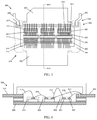
- FIG. 1 is a schematic diagram of an RF amplifier device 100.
- Device 100 includes an input lead 102, an input impedance matching circuit 110, a transistor 120, an output impedance matching circuit 130, an envelope frequency termination circuit 150, and an output lead 104, in an embodiment.
- the output impedance matching circuit 130 and the envelope frequency termination circuit 150 may be referred to collectively as an "output circuit.”
- transistor 120 and various elements of the input and output impedance matching circuits 110, 130 and the envelope frequency termination circuit 150 are shown as singular components, the depiction is for the purpose of ease of explanation only.
- transistor 120 and/or certain elements of the input and output impedance matching circuits 110, 130 and the envelope frequency termination circuit 150 each may be implemented as multiple components (e.g., connected in parallel or in series with each other), and examples of such embodiments are illustrated in the other Figures and described later.
- embodiments may include single-path devices (e.g., including a single input lead, output lead, transistor, etc.), dual-path devices (e.g., including two input leads, output leads, transistors, etc.), and/or multi-path devices (e.g., including two or more input leads, output leads, transistors, etc.).
- the number of input/output leads may not be the same as the number of transistors (e.g., there may be multiple transistors operating in parallel for a given set of input/output leads).
- Input lead 102 and output lead 104 each include a conductor, which is configured to enable the device 100 to be electrically coupled with external circuitry (not shown). More specifically, input and output leads 102, 104 are physically located between the exterior and the interior of the device's package. Input impedance matching circuit 110 is electrically coupled between the input lead 102 and a first terminal of transistor 120, which is also located within the device's interior, and output impedance matching circuit 130 and envelope frequency termination circuit 150 are electrically coupled between a second terminal of transistor 120 and the output lead 104.
- transistor 120 is the primary active component of device 100.
- Transistor 120 includes a control terminal and two current conducting terminals, where the current conducting terminals are spatially and electrically separated by a variable-conductivity channel.
- transistor 120 may be a field effect transistor (FET) (such as a metal oxide semiconductor FET (MOSFET)) or a high electron mobility transistor (HEMT), each of which includes a gate (control terminal), a drain (a first current conducting terminal), and a source (a second current conducting terminal).
- FET field effect transistor
- HEMT high electron mobility transistor
- transistor 120 may be a bipolar junction transistor (BJT).
- references herein to a "gate,” “drain,” and “source,” are not intended to be limiting, as each of these designations has analogous features for a BJT implementation (e.g., a base, collector, and emitter, respectively).
- the gate of transistor 120 is coupled to the input impedance matching circuit 110, the drain of transistor 120 is coupled to the output impedance matching circuit 130 and the envelope frequency termination circuit 150, and the source of transistor 120 is coupled to ground (or another voltage reference).
- the current between the current conducting terminals of transistor 120 may be modulated.
- Input impedance matching circuit 110 is configured to raise the impedance of device 100 to a higher (e.g., intermediate or higher) impedance level (e.g., in a range from about 2 to about 10 Ohms or higher). This is advantageous in that it allows the printed circuit board level (PCB-level) matching interface from a driver stage to have an impedance that can be achieved in high-volume manufacturing with minimal loss and variation (e.g., a "user friendly" matching interface).
- Input impedance matching circuit 110 is coupled between the input lead 102 and the control terminal (e.g., gate) of the transistor 120.
- input impedance matching circuit 110 is a low pass circuit, which includes two inductive elements 112, 116 (e.g., two sets of bondwires) and a shunt capacitor 114.
- a first inductive element 112 e.g., a first set of bondwires
- a second inductive element 116 e.g., a second set of bondwires
- the second terminal of capacitor 114 is coupled to ground (or another voltage reference).
- the combination of inductive elements 112, 116 and shunt capacitor 114 functions as a low-pass filter.
- the series combination of inductive elements 112, 116 may have a value in a range between about 50 picohenries (pH) to about 3 nanohenries (nH), and shunt capacitor 114 may have a value in a range between about 2 picofarads (pF) to about 100 pF.
- Output impedance matching circuit 130 is configured to match the output impedance of device 100 with the input impedance of an external circuit or component (not shown) that may be coupled to output lead 104. Output impedance matching circuit 130 is coupled between the first current conducting terminal (e.g., drain) of transistor 120 and the output lead 104. According to an embodiment, output impedance matching circuit 130 includes three inductive elements 132, 136, 140 (e.g., three sets of bondwires) and two capacitors 134, 138. Output impedance matching circuit 130 includes a high-pass matching circuit 131 (including inductive element 132 and capacitor 134) and a low-pass matching circuit 135 (including inductive elements 136, 140 and capacitor 138), in an embodiment.
- inductive elements 136, 140 e.g., third and fourth sets of bondwires
- L LP1 and L LP2 are coupled in series between the first current conducting terminal (e.g., drain) of transistor 120 and the output lead 104, with node 137 between inductive elements 136, 140.
- Capacitor 138 also referred to herein as “C LP”
- C LP has a first terminal coupled to node 137, and a second terminal coupled to a ground node 157, which in turn may be coupled to ground (or to another voltage reference).
- the combination of inductive elements 136, 140 and capacitor 138 functions as a first (low-pass) matching stage.
- the series combination of inductive elements 136, 140 may have a value in a range between about 40 pH to about 3 nH, and capacitor 138 may have a value in a range between about 2 pF to about 80 pF, although these components may have values outside of these ranges, as well.
- capacitor 138 may be replaced with a conductor-backed, low impedance transmission line, which includes a forward current carrying path (e.g., lateral conductor 1132, FIG. 11 ) and a ground plane (e.g., conductive layer 1157, FIG. 11 ) that are separated by dielectric material (e.g., dielectric layer(s) 1138, FIG. 11 ). Because there would be some capacitive interaction between the forward current carrying path and the ground plane, such a conductor-backed transmission line theoretically could be referred to as a capacitor (or a ceramic capacitor when the dielectric material is a ceramic).
- a conductor-backed, low impedance transmission line which includes a forward current carrying path (e.g., lateral conductor 1132, FIG. 11 ) and a ground plane (e.g., conductive layer 1157, FIG. 11 ) that are separated by dielectric material (e.g., dielectric layer(s) 1138, FIG. 11 ). Because there would be some capacitive interaction between the forward
- inductive element 132 e.g., a fifth set of bondwires
- L shunt first terminal of capacitor 134
- C shunt first terminal of capacitor 134
- a second terminal of capacitor 134 is coupled to a ground node 157.
- inductive element 132 may have a value in a range between about 80 pH to about 3 nH
- capacitor 134 may have a value in a range between about 50 pF to about 500 pF, although these components may have values outside of these ranges, as well.
- Envelope frequency termination circuit 150 is coupled between the RF cold point (at node 151) and ground node 157, in an embodiment. Envelope frequency termination circuit 150 functions to improve the low frequency resonance of device 100 caused by the interaction between the output impedance matching circuit 130 and the bias feeds by presenting a high impedance at RF frequencies. Envelope frequency termination circuit 150 essentially is "invisible" from a matching standpoint, as it only effects the output impedance at envelope frequencies (i.e., envelope frequency termination circuit 150 provides terminations for the envelope frequencies of device 100).
- envelope frequency termination circuit 150 includes a resistor 152, an inductance 154, and a capacitor 156 coupled in series.
- a first terminal of resistor 152 referred to herein as an “envelope resistor” or “R env ,” is coupled to node 151 (i.e., the RF cold point).
- a second terminal of envelope resistor 152 is coupled to a first terminal of inductance 154, revered to herein as an "envelope inductor” or "L env. "
- a second terminal of inductance 154 is coupled to capacitor 156, referred to herein as an "envelope capacitor” or "C env.
- a second terminal of the envelope capacitor 156 is coupled to the ground node 157, in an embodiment.
- Envelope resistor 152 may have a value in a range between about 0.1 Ohm to about 2 Ohm
- envelope inductance 154 may have a value that is less than about 25 - 500 pH
- envelope capacitor 156 may have a value in a range between about 5 nanofarads (nF) to about 1 microfarad ( ⁇ F), although these components may have values outside of these ranges, as well.
- envelope inductance 154 is shown to include a single lumped element in FIG.
- envelope inductance 154 actually may be made up of one or more distinct inductors (e.g., inductor 754, 1054, FIGs 7 , 10 ) and additional small inductances associated with other conductive features (e.g., conductive vias and portions of conductive traces) present in the conductive path between RF cold point node 151 and ground node 157.
- inductors e.g., inductor 754, 1054, FIGs 7 , 10
- additional small inductances associated with other conductive features e.g., conductive vias and portions of conductive traces
- capacitors 134, 138, 156, envelope resistor 152, and envelope inductor 154 may be integrally formed portions of the aforementioned multi-dielectric ceramic device (e.g., multi-dielectric ceramic device 700, FIG. 7 ), as indicated by the dashed box 160 encompassing these components.
- the multi-dielectric ceramic device may include two capacitors (e.g., capacitors 134 and 156, or capacitors 156 and 138) with different dielectric materials between their respective electrodes.
- Inclusion of the third capacitor, inductor 154, and/or resistor 152 provide for increased integration of the components of the output circuit, with potential benefits in terms of smaller device size, lower device cost, and/or improved device performance.
- FIG. 2 is a top view of an example of a packaged RF amplifier device 200 that embodies the circuit of FIG. 1 , in accordance with an example embodiment. More particularly, the interconnected electrical components and elements of device 200 may be modeled by the schematic diagram of FIG. 1 . For enhanced understanding, FIG. 2 should be viewed in parallel with FIG. 3 , which is a cross-sectional, side view of the RF amplifier device 200 of FIG. 2 along line 3-3.
- Device 200 includes an input lead 202 (e.g., input lead 102, FIG. 1 ), an output lead 204 (e.g., output lead 104, FIG. 1 ), bias leads 205, a flange 206, an isolation structure 208, and three parallel amplification paths (i.e., three parallel instantiations of circuit 100, FIG. 1 ) electrically coupled between the input and output leads 202, 204.
- Each amplification path includes an input impedance matching circuit 210 (e.g., input impedance matching circuit 110, FIG. 1 ), a transistor 220 (e.g., transistor 120, FIG. 1 ), an output impedance matching circuit 230 (e.g., output impedance matching circuit 130, FIG.
- envelope frequency termination circuit 250 e.g., envelope frequency termination circuit 150, FIG. 1 .
- portions of the output impedance matching circuit 230 and the envelope frequency termination circuit 250 are implemented in a multi-dielectric ceramic device 260, in accordance with an embodiment.
- Flange 206 includes a rigid electrically-conductive substrate, which has a thickness that is sufficient to provide structural support for other components and elements of device 200.
- flange 206 may function as a heat sink for transistors 220 and other devices mounted on flange 206.
- Flange 206 has a top and bottom surface and a substantially-rectangular perimeter that corresponds to the perimeter of the device 200. In FIG. 2 , only a central portion of the top surface of flange 206 is visible through an opening in isolation structure 208. At least the surface of flange 206 is formed from a layer of conductive material, and possibly all of flange 206 is formed from bulk conductive material. Alternatively, flange 206 may have one or more layers of non-conductive material below its top surface. Either way, flange 206 has a conductive top surface. When device 200 is incorporated into a larger electrical system, flange 206 may be used to provide a ground reference for the device 200.
- Isolation structure 208 is formed from a rigid, electrically insulating material (i.e., a material with a dielectric constant in a range from about 3.0 to about 10.0, although materials with higher or lower dielectric constants may be used), and has a top surface and an opposed bottom surface.
- the term "isolation structure,” as used herein, refers to a structure that provides electrical isolation between conductive features of a device (e.g., between leads 202, 204 and flange 206).
- isolation structure 208 may be formed from inorganic materials (e.g., ceramic such as aluminum oxide, aluminum nitride, and so on) and/or organic materials (e.g., one or more polymers or printed circuit board (PCB) materials).
- isolation structure 208 comprises PCB materials (e.g., the isolation structure 208 essentially includes a single or multi-layer PCB)
- conductive layers e.g., copper layers
- a conductive layer on the top surface of the isolation structure 208 may be patterned and etched to form a leadframe (including leads 202, 204) for the device 200, and a conductive layer on the bottom surface of the isolation structure 208 may be coupled to the flange 206.
- conductive layers may be excluded from the top and/or bottom surface of the isolation structure 208.
- leads e.g., leads 202, 204 may be coupled to the isolation structure 208 using metallurgic connection or epoxy (or other adhesive materials), and/or the isolation structure 208 may be coupled to the flange 206 using metallurgic connection or epoxy (or other adhesive materials). In still other embodiments, the isolation structure 208 may be milled at the portion of its top surface to which a lead is attached.
- Isolation structure 208 has a frame shape, in an embodiment, which includes a substantially enclosed, four-sided structure with a central opening. Isolation structure 208 may have a substantially rectangular shape, as shown in FIG. 2 , or isolation structure 208 may have another shape (e.g., annular ring, oval, and so on). Isolation structure 208 may be formed as a single, integral structure, or isolation structure 208 may be formed as a combination of multiple members. For example, in an alternate embodiment, isolation structure 208 may include multiple portions that contact each other or that are spatially separated from each other (e.g., isolation structure 208 may have one portion isolating input lead 202 from flange 206, and another portion isolating output lead 204 from flange 206). In addition, isolation structure 208 may be formed from a homogenous material, or isolation structure 208 may be formed from multiple layers.
- the input and output leads 202, 204 and the bias leads 205 are mounted on a top surface of the isolation structure 208 on opposed sides of the central opening, and thus the input and output leads 202, 204 and the bias leads 205 are elevated above the top surface of the flange 206, and are electrically isolated from the flange 206.
- the leads 202, 204, 205 may be soldered or otherwise attached to metallization (not shown) on a top surface of isolation structure 208 (e.g., a metallurgic connection).
- the leads 202, 204, 205 are oriented in order to allow for attachment of bondwires (e.g., bondwires 212, 240) between the leads 202, 204, 205 and components and elements within the central opening of isolation structure 208.
- bondwires e.g., bondwires 212, 240
- bias leads 205 are electrically coupled together with a bar-shaped conductor 207, which also is coupled to the top surface of isolation structure 208.
- conductor 207 includes metallization on a top surface of isolation structure 208. Proximal ends of bias leads 205 are coupled to opposite ends of conductor 207, in an embodiment. Bondwires (not shown) are electrically coupled between conductor 207 and a bias point (e.g., cold point node 151,251, FIGs 1 , 2 ).
- Bias leads 205 extend from the device 200, once packaged, so that their distal ends are exposed and may be coupled to a PCB of a larger system to receive a bias voltage. Accordingly, inclusion of bias leads 205 eliminates the need for bias leads on the PCB itself. According to an embodiment, each bias lead 205 has a length corresponding to lambda/4, although each bias lead 205 may have a different length, as well.
- An advantage of including bias leads 205 as part of device 200 is that the bias leads 205 remove the need for quarter wave bias feeds, as additional large value de-coupling capacitors may be connected between the bias leads 205 and ground as the bias leads 205 exit the device package.
- Another embodiment may include a four-lead device with an input lead, an output lead, and two bias leads coupled to the input impedance matching circuit.
- Yet another embodiment includes a six-lead device with an input lead, an output lead, two bias leads coupled to the output impedance matching circuit and two bias leads coupled to the input impedance matching circuit.
- only a single bias lead may be coupled to the input and/or output impedance matching circuits (e.g., particularly for embodiments in which there are more than two RF leads, such as in dual-path and multi-path devices).
- Transistors 220 and various elements 214, 260 of the input and output impedance matching circuits 210, 230 and the envelope frequency termination circuit 250 are mounted on a generally central portion of the top surface of a flange 206 that is exposed through the opening in isolation structure 208.
- the transistors 220 and elements 214, 260 of the input and output impedance matching circuits 210, 230 and the envelope frequency termination circuit 250 may be coupled to flange 206 using conductive epoxy, solder, solder bumps, sintering, and/or eutectic bonds.
- an "active device area” corresponds to a portion of a device on which one or more active devices (e.g., transistor 220) are mounted (e.g., the portion of the conductive surface of flange 206 that exposed through the opening in isolation structure 208).
- Each of transistors 220 has a control terminal (e.g., a gate) and two current conducting terminals (e.g., a drain and a source).
- the control terminal of each transistor 220 is coupled to the input lead 202 through an input impedance matching circuit 210 (e.g., input impedance matching circuit 110, FIG. 1 ).
- one current conducting terminal (e.g., the drain) of each transistor 220 is coupled to the output lead 204 through an output impedance matching circuit 230 (e.g., output impedance matching circuit 130, FIG. 1 ), and the other current conducting terminal (e.g., the source) is coupled to the flange 206 (e.g., to a ground reference node for the device 200).
- each input impedance matching circuit 210 includes two inductive elements 212, 216 (e.g., inductive elements 112, 116, FIG. 1 ) and a capacitor 214 (e.g., capacitor 114, FIG. 1 ).
- Each inductive element 212, 216 is formed from a plurality of parallel, closely-spaced sets of bondwires.
- a first inductive element 212 e.g., inductive element 112, FIG. 1
- a second inductive element 216 e.g., inductive element 116, FIG.
- Capacitor 214 may be, for example, a discrete silicon capacitor (e.g., comprised of a silicon substrate with a top surface corresponding to a first terminal, and a bottom surface corresponding to a second terminal), a discrete ceramic capacitor, or another type of capacitor. Bondwires 212, 216 are attached to a conductive top plate at the top surface of capacitor 214.
- each output impedance matching circuit 230 includes three inductive elements 232, 236, 240 (e.g., L shunt 132, L LP1 136, and L LP2 140, FIG. 1 ) and two capacitors (e.g., C shunt 134 and C LP 138, FIG. 1 ), where the capacitors form portions of multi-dielectric ceramic device 260, in an embodiment.
- each inductive element 232, 236, 240 is formed from a plurality of parallel, closely-spaced sets of bondwires.
- shunt inductive element 232 e.g., L shunt 132, FIG.
- first bond pad 251 e.g., corresponding to RF cold point node 151, FIG. 1 .
- the first bond pad 251 is electrically coupled to a shunt capacitor (e.g., C shunt 134, FIG. 1 ) within the multi-dielectric ceramic device 260.
- a first series inductive element 236 e.g., L LP1 136, FIG.
- a second bond pad 237 (e.g., corresponding to node 137, FIG. 1 ) on the top surface of the multi-dielectric ceramic device 260.
- the second bond pad 237 is electrically coupled to a low pass matching capacitor (e.g., C LP 138, FIG. 1 ) within the multi-dielectric ceramic device 260.
- a second series inductive element 240 (e.g., L LP2 140, FIG. 1 ) is coupled between the second bond pad 237 and the output lead 204. Second terminals of the shunt and LP-match capacitors within the multi-dielectric ceramic device 260 are coupled to the flange 206 (e.g., to ground).
- device 200 is incorporated in an air cavity package, in which transistors 220 and various impedance matching and envelope frequency termination elements are located within an enclosed air cavity 312.
- the air cavity is bounded by flange 206, isolation structure 208, and a cap 310 overlying and in contact with the isolation structure 208 and leads 202, 204.
- a device may be incorporated into an overmolded package (i.e., a package in which the electrical components within the active device area are encapsulated with a non-conductive molding compound, and in which portions of the leads 202, 204 also may be encompassed by the molding compound).
- the output impedance matching circuit 130, 230 includes a high-pass shunt circuit 131 and a low-pass, LP-match circuit 135 (e.g., including inductive elements 136, 140 or bondwires 236, 240 and capacitor 138).
- the low-pass matching circuit 135 may be replaced with a differently-configured matching circuit.
- FIG. 4 is a schematic diagram of an RF amplifier 400 with a second matching circuit 435 (e.g., a low-pass matching circuit with a very high frequency resonance) forming a portion of its output impedance matching circuit 430, in accordance with another example embodiment.
- RF amplifier 400 may be substantially similar to the amplifier 100 of FIG. 1 , and like reference numbers are used in both drawings to indicate elements that may be substantially the same between the two embodiments.
- inductive element 436 is coupled directly between the first current conducting terminal (e.g., drain) of transistor 120 and the output lead 104.
- the high-pass matching circuit 435 which includes a “bond back” or “BB” inductive element 440 coupled in series with a BB capacitor 438, is coupled between the output lead 104 and the ground node 152. More specifically, L BB 440 is coupled between the output lead 104 and a node 437, and C BB 438 is coupled between node 437 and the ground node 157.
- L series 436 may have a value in a range between about 50 pH to about 3 nH
- L BB 440 may have a value in a range between about 50 pH to about 500 pH
- C BB 438 may have a value in a range between about 2 pF to about 50 pF, although these components may have values outside of these ranges, as well.
- capacitors 134, 438, 156, envelope resistor 152, and envelope inductor 154 may be integrally formed portions of the aforementioned multi-dielectric ceramic device (e.g., multi-dielectric ceramic device 700, FIG. 7 ), as indicated by the dashed box 460 encompassing these components.
- the multi-dielectric ceramic device may include two capacitors (e.g., capacitors 134 and 156, or capacitors 156 and 438) with different dielectric materials between their respective electrodes.
- FIG. 5 is a top view of an example of a packaged RF amplifier device 500 that embodies the circuit of FIG. 4 , in accordance with an example embodiment. More particularly, the interconnected electrical components and elements of device 500 may be modeled by the schematic diagram of FIG. 4 . For enhanced understanding, FIG. 5 should be viewed in parallel with FIG. 6 , which is a cross-sectional, side view of the RF amplifier device 500 of FIG. 5 along line 6-6.
- packaged RF amplifier device 500 may be substantially similar to the device 200 of FIGs 2 and 3 , and like reference numbers are used in both drawings to indicate elements that may be substantially the same between the two embodiments.
- each output impedance matching circuit 530 includes three inductive elements 232, 536, 540 (e.g., L shunt 132, L series 436, and L BB 440, FIG. 4 ) and two capacitors (e.g., C shunt 134 and C BB 438, FIG. 4 ), where the capacitors form portions of multi-dielectric ceramic device 560 (e.g., multi-dielectric ceramic device 460, FIG. 4 ), in an embodiment.
- each inductive element 232, 536, 540 is formed from a plurality of parallel, closely-spaced sets of bondwires.
- shunt inductive element 232 e.g., L shunt 132, FIG.
- a series inductive element 536 (e.g., L series 436, FIG. 4 ) includes a plurality of bondwires coupled between the first current conducting terminal of transistor 220 and the output lead 204.
- a bond back inductive element 540 (e.g., L BB 440, FIG. 4 ) is coupled between the output lead 204 and a second bond pad 237 (e.g., corresponding to node 437, FIG. 4 ) on the top surface of the multi-dielectric ceramic device 260.
- the second bond pad 437 is electrically coupled to a bond back capacitor (e.g., C BB 438, FIG. 4 ) within the multi-dielectric ceramic device 560.
- Second terminals of the shunt and bond back capacitors within the multi-dielectric ceramic device 560 are coupled to the flange 206 (e.g., to ground).
- FIG. 7 is a top view of a multi-dielectric ceramic device 700 (e.g., device 160, 260, 460, 560, FIGs 1-5 ) suitable for use in an output circuit (e.g., an out impedance matching circuit 130, 230, 430, 530 and envelope frequency termination circuit 150, 250, FIGs 1-5 ) in a packaged RF amplifier device (e.g., device 200, 400, FIGs 2 , 4 ), in accordance with an example embodiment.
- FIG. 7 should be viewed in conjunction with FIGs 8 and 9 , which illustrate cross-sectional, side views of multi-dielectric ceramic device 700 along lines 8-8 and 9-9, respectively.
- Multi-dielectric ceramic device 700 includes several of passive components of an output circuit, such as the components encompassed by box 160, FIG. 1 or by box 460, FIG. 4 .
- the bondwires 732, 736, 740 ( FIG. 8 ) coupled to multi-ceramic device 700 are analogous to the inductive components 132, 136, 140, respectively, and bondwires 232, 236, 240, respectively, of FIGs 1 and 2 .
- bondwires alternatively could be coupled to multi-ceramic device 700 in a manner that is analogous, instead, to the inductive components 132, 440 and bondwires 232, 540 of FIGs 4 and 5 .
- multi-ceramic device 700 may be used in either circuit configuration, although the values of some of the components may be altered based on the circuit configuration.
- multi-dielectric ceramic device 700 includes a first shunt capacitor 734 (e.g., C shunt 134, FIGs 1 , 4 ), a second shunt capacitor 738 (e.g., C LP 138 or C bb 438, FIGs 1 , 4 ), an envelope resistor 752 (e.g., R env 152, FIGs 1 , 4 ), an envelope inductor 754 (e.g., L env 154, FIGs 1 , 4 ), and an envelope capacitor 756 (e.g., C env 156, FIGs 1 , 4 ).
- a first shunt capacitor 734 e.g., C shunt 134, FIGs 1 , 4
- a second shunt capacitor 738 e.g., C LP 138 or C bb 438, FIGs 1 , 4
- an envelope resistor 752 e.g., R env 152, FIGs 1 , 4
- dashed boxes 734, 738, 754, 756 indicate the approximate area of each electrode plate for capacitors 734, 738, 756, and dashed box 754 indicates the approximate area occupied by each inductor layer of inductor 754.
- dashed box 754 indicates the approximate area occupied by each inductor layer of inductor 754.
- multi-dielectric ceramic device 700 has a substantially rectangular footprint, with first, second, third, and fourth sides 770, 771, 772, 773 that extend between first and second opposed surfaces 802, 804 (referred to as top and bottom surfaces herein, respectively).
- device 700 includes one or more first contact pads 751 (e.g., corresponding to RF cold point node 151, FIGs 1 , 4 ) exposed at the top surface 802, and one or more second contact pads 737 (e.g., corresponding to node 137, 437, FIGs 1 , 4 ) that also are exposed at the top surface 802.
- a layer of passivation 864 may overlie portions of the top surface 802 other than the contact pads 751, 737. Further, a conductive layer 857 (e.g., corresponding to ground node 157, FIGs 1 , 4 ) is coupled to the bottom surface 804 of the device 700.
- Contact pads 751, 737 include bondwire landing sites, indicated with "X"s, which are configured to enable bondwires (e.g., bondwires 732, 736, 740) to be coupled to the contact pads 751, 737.
- device 700 includes a plurality of passive components, as mentioned above, that are electrically coupled between the contact pads 751, 737 and the conductive layer 857.
- the passive components are formed as portions of a plurality of first ceramic layers 810-816, second ceramic layers 860-863, and conductive layers 820-825, 870-873 that are sandwiched between the ceramic layers 810-816, 860-863.
- the ceramic layers 810-816, 860-863 and conductive layers 820-825, 870-873 are co-fired together using a relatively low temperature process (e.g., device 700 is a low temperature co-fired ceramic (LTCC) device).
- LTCC low temperature co-fired ceramic
- multi-dielectric ceramic device 700 is a monolithic device, in an embodiment.
- the first ceramic layers 810-816 include a first ceramic material that has a first dielectric constant and a first Q factor
- the second ceramic layers 860-863 include a second ceramic material that has a second dielectric constant and a second Q factor that are different from the first dielectric constant and first Q factor.
- the dielectric constants and Q factors may be voltage and/or frequency and/or temperature dependent.
- the first dielectric material is a relatively lossy material (e.g., low Q factor) with a relatively high dielectric constant (e.g., in a range of about 300-2000, such as about 1000), and the second dielectric material is a low loss material (e.g., high Q factor) with a relatively low dielectric constant (e.g., in a range of about 8 to about 200, such as about 80).
- the first ceramic layers 810-816 may include relatively low-Q, high dielectric constant material(s), such as barium titanate (BaTiO3), relaxor ferroelectric, other alkaline earth titanates, or other relatively low-Q materials.
- the second ceramic layers 860-863 may include relatively high-Q, low dielectric constant material(s), such as aluminum nitrate (AlN), titanium dioxide, magnesium silicate, or other relatively high-Q materials.
- the first and second ceramic layers 810-816, 860-863 may include various additives, which may affect voltage and temperature stability of the materials, and/or may affect other material characteristics.
- Conductive layers 820-825, 830, 857, and 870-873 may be formed from any of a variety of metals and/or metal alloys.
- conductive layers 820-825, 830, 857, and 870-873 may be formed from one or more materials selected from a noble metal, palladium, gold, platinum, silver, nickel, tin-lead, alloys or combinations thereof, and other suitable materials.
- conductive layers 820-825, 830, 857, and 870-873 are formed from a material with a melting point that is higher than firing and/or sintering temperatures that are reached during fabrication of the multi-dielectric ceramic device 700 (e.g., a conductive material that yields a continuous conductive film after sintering or firing, and which does not diffuse into or react with the ceramic dielectric).
- conductive vias 835, 855, 831, 851, 834, 833 electrically couple portions of the conductive layers 820-825, 830, 857, and 870-873, thus providing interconnection of the various components within device 700.
- the conductive vias 835, 855, 831, 851, 834, 833 may be formed from the same or different materials from the conductive layers 820-825, 830, 857, and 870-873.
- the first shunt capacitor 734 (e.g., C shunt 134, FIGs 1 , 4 ) is a multi-layer capacitor formed from portions of conductive layers 870-873, ceramic layers 861-863, and vias 835, 834. More specifically, portions of conductive layers 871 and 873 that are electrically coupled through vias 834 correspond to plates of a first electrode of capacitor 734, and portions of conductive layers 870 and 872 that are electrically coupled through vias 835 correspond to plates of a second electrode of capacitor 734.
- the first and second electrode plates are interleaved with each other, with portions of ceramic layers 861-863 (or ceramic material 865) electrically separating the electrode plates of the first electrode from the electrode plates of the second electrode.
- Conductive layers 871 and 873 may be electrically connected to each other through vias 834, and conductive layers 870 and 872 (or the second electrode plates of capacitor 734) may be electrically connected to each other through vias 835, as shown in FIGs 8 and 9 .
- first and second electrode plates alternate in the stack, the set of alternate electrodes that forms the first electrode are coupled with a first termination (e.g., vias 834), and the set of alternate electrodes that forms the second electrode are coupled with a second termination (e.g., vias 835).
- some or all of conductive layers 870-873 may extend to one of the sides 770, 771, 773 of device 700, and conductive material coupled to (e.g., deposited on) the sides 770, 771, 773 and in contact with the edges of conductive layers 870-873 may provide electrical connectivity between the first and second electrode plates.
- vias 835, 834 may be more generally referred to as "vertical conductors," which term encompasses embodiments that use conductive structures other than vias.
- a portion of the uppermost conductive layer 873 serves as a contact pad 751 (e.g., corresponding to RF cold point node 151, FIGs 1 , 4 ).
- This contact pad 751 may have dual functions as both a connection point for bondwires 732 (e.g., inductive element 132 or bondwires 232, FIGs 1-6 ) and the uppermost electrode plate of the first electrode of capacitor 734.
- contact pad 751 may be implemented as a distinct element, in an alternate embodiment (i.e., contact pad 751 may not be positioned or configured to function as an electrode plate, in an alternate embodiment).
- contact pad 751 is electrically coupled to the first electrode of capacitor 734 (i.e., portions of conductive layers 871, 873 and vias 834).
- the second electrode of capacitor 734 i.e., portions of conductive layers 870, 872 and vias 835) is electrically coupled to the bottom conductive layer 857 (e.g., to ground node 157, FIGs 1 , 4 ) through vias 835, 833.
- vias 835 and 833 are shown to be aligned in FIGs 8 and 9 , vias 835 and 833 alternatively may be offset from each other in the vertical direction.
- capacitor 734 is a multi-layer capacitor (i.e., a capacitor in which at least one electrode is implemented in the form of a plurality of electrically-coupled electrode plates that are interleaved with electrode plate(s) of the other electrode).
- capacitor 734 may include more or fewer interleaved electrode plates than are illustrated, or just one electrode plate for each electrode.
- capacitor 734 may be described as a ceramic capacitor formed from a stack that includes a first electrode, a second electrode, and a first ceramic material 865 between the first and second electrodes.
- the first ceramic material 865 (from which ceramic layers 861-863 are formed) has a first dielectric constant and a first quality factor.
- the second shunt capacitor 738 (e.g., C LP 138 or C bb 438, FIGs 1 , 4 ). As indicated most clearly in FIG. 7 , shunt capacitor 738 is implemented as six capacitors in parallel with each other. In alternate embodiments, shunt capacitor 738 may be implemented using a single capacitor, or using more or fewer than six parallel and/or series coupled capacitors. According to an embodiment, the second shunt capacitor 738 is formed from portions of conductive layers 870 and 873, and ceramic layers 861-863. More specifically, a portion of conductive layer 873 corresponds to a first electrode plate of capacitor 738, and a portion of conductive layer 870 corresponds to a second electrode plate of capacitor 738. Portions of ceramic layers 861-863 (or ceramic material 866) electrically separate the first and second electrode plates.
- a portion of the uppermost conductive layer 873 corresponds to contact pad 737 (e.g., corresponding to node 137, 437, FIGs 1 , 4 ).
- This contact pad 737 may have dual functions as both a connection point for bondwires 736 and/or 740 (e.g., inductive elements 136, 140, 440 or bondwires 236, 240, 540, FIGs 1-6 ) and the first electrode of capacitor 738.
- contact pad 737 may be implemented as a distinct element, in an alternate embodiment (i.e., contact pad 737 may not be positioned or configured to function as an electrode plate, in an alternate embodiment).
- contact pad 737 is electrically coupled to the first electrode of capacitor 738 (e.g., a portion of conductive layer 873).
- the second electrode of capacitor 738 e.g., a portion of conductive layer 870
- the bottom conductive layer 857 e.g., to ground node 157, FIGs 1 , 4 .
- capacitor 738 is a two-layer capacitor (i.e., a capacitor in which each electrode is implemented in the form of a single electrode plate).
- capacitor 738 may be implemented as a multi-layer capacitor (i.e., including multiple interleaved electrode plates).
- capacitor 738 may be described as a ceramic capacitor formed from a stack that includes a first electrode, a second electrode, and ceramic material (e.g., ceramic material 866) between the first and second electrodes.
- ceramic material 866 is the same as ceramic material 865, which separates the electrodes of capacitor 734.
- ceramic material 866 may include different materials from ceramic material 865.
- the envelope capacitor 756 (e.g., C env 156, FIGs 1 , 4 ) is a multi-layer capacitor formed from portions of conductive layers 820-825, ceramic layers 811-815, and vias 855, 831, 833. More specifically, portions of conductive layers 821, 823, 825 that are electrically coupled through vias 855 correspond to plates of a first electrode of capacitor 756, and portions of conductive layers 820, 822, 824 that are electrically coupled through vias 831, 833 correspond to plates of a second electrode of capacitor 756.
- the first and second electrode plates are interleaved with each other, with portions of ceramic layers 811-815 (or ceramic material 817) electrically separating the electrode plates of the first electrode from the electrode plates of the second electrode.
- Conductive layers 821, 823, 825 may be electrically connected to each other through vias 855, and conductive layers 820, 822, 824 (or the second electrode plates of capacitor 756) may be electrically connected to each other through vias 831, 833, as shown in FIGs 8 and 9 .
- conductive layers 820-825 may extend to one of the sides 770-774 of device 700, and conductive material coupled to (e.g., deposited on) the sides 770-774 and in contact with the edges of conductive layers 820-825 may provide electrical connectivity between the first and second electrode plates.
- vias 855, 831, 833 may be more generally referred to as "vertical conductors," which term encompasses embodiments that use conductive structures other than vias.
- the first electrode of capacitor 756 i.e., portions of conductive layers 821, 823, 825) are electrically coupled to the contact pad 751 through the series combination of envelope resistor 752, envelope inductor 754 and vias 855.
- the second electrode of capacitor 756 i.e., portions of conductive layers 820, 822, 824 is electrically coupled to the bottom conductive layer 857 (e.g., to ground node 157, FIGs 1 , 4 ) through vias 831 and 833.
- capacitor 756 is a multi-layer capacitor. In alternate embodiments, capacitor 756 may include more or fewer interleaved electrode plates than are illustrated, or just one electrode plate for each electrode. In any event, capacitor 756 may be described as a ceramic capacitor formed from a stack that includes a first electrode, a second electrode, and a second ceramic material 817 between the first and second electrodes. As discussed previously, the second ceramic material 817 (from which ceramic layers 811-815 are formed) has a second dielectric constant and a second quality factor that are different from the first dielectric constant and the first quality factor of the first ceramic material 865, 866 included in capacitors 734, 738. According to an embodiment, ceramic material 817 has a significantly lower Q (and possibly a higher dielectric constant) than ceramic material 865, 866.
- an embodiment of a baseband termination circuit includes a series combination of an envelope resistor 752 (e.g., R env 152, FIGs 1 , 4 ), an envelope inductor 754 (e.g., L env 154, FIGs 1 , 4 ), and envelope capacitor 756 (e.g., C env 156, FIGs 1 , 4 ).
- an envelope resistor 752 e.g., R env 152, FIGs 1 , 4
- an envelope inductor 754 e.g., L env 154, FIGs 1 , 4
- envelope capacitor 756 e.g., C env 156, FIGs 1 , 4
- envelope resistor 752 is coupled to the top surface 802 of device 700, and is electrically coupled between contact pad 751 (e.g., RF cold point node 151, FIGs 1 , 4 ) and a first terminal 753 ofthe envelope inductor 754 (e.g., node 153, FIGs 1 , 4 ).
- contact pad 751 e.g., RF cold point node 151, FIGs 1 , 4
- first terminal 753 ofthe envelope inductor 754 e.g., node 153, FIGs 1 , 4
- envelope resistor 752 is a thick- or thin-film resistor that is formed on the surface 802 of the device 700.
- envelope resistor 752 may be a discrete component mounted to surface 802.
- envelope inductor 754 (e.g., L env 154, FIGs 1 , 4 ) is implemented as two inductors in parallel with each other.
- the envelope inductor 754 may be implemented using a single inductor, or using more than two parallel and/or series coupled inductors.
- the envelope inductor 754 includes one or more multi-layer inductors, each formed from portions of conductive layers 870-873, ceramic layers 861-863, and vias 851, 852, 853.
- conductive layers 870-873 are electrically coupled through vias 851-853 in a manner that results in an undulating or zig-zag path between the first terminal 753 ofthe envelope inductor 754 (e.g., node 153, FIGs 1 , 4 ) and the second terminal 854 of the envelope inductor 754.
- envelope inductor 754 is formed from a plurality of serially-coupled inductor segments formed from multiple conductive layers 870-873 that are separated from each other by the ceramic material of ceramic layers 861-863.
- the second terminal 854 of the envelope inductor 754 is electrically coupled to the first electrode of envelope capacitor 756 through vias 855.
- some or all of conductive layers 870-873 may extend to one ofthe sides 770-774 of device 700, and conductive material coupled to (e.g., deposited on) the sides 770-774 and in contact with the edges of conductive layers 870-873 may provide electrical connectivity between the portions of layers 870-873 that form the envelope inductor 754.
- envelope inductor 754 is a multi-layer inductor.
- envelope inductor 754 may be a discrete component mounted to surface 802, or may be formed from a plurality of bondwires that are interconnected in series with envelope resistor 752 between contact pad 751 (e.g., the RF cold point node 151, FIGs 1 , 4 ) and envelope capacitor 756.
- FIGs 1 , 4 , and 6-8 depict the baseband termination circuit as including a series combination of envelope resistor 152, 752, envelope inductor 154, 754, and envelope capacitor 156, 756, in that order, the envelope resistor 152, 752, envelope inductor 154, 754, and envelope capacitor 156, 756 could be series coupled in different orders, in alternate embodiments.
- forward current (indicated by dashed line 880) is carried through bondwires 736 and 740 over device 700.
- Reverse current (indicated by dashed line 881), in contrast, is carried through a reverse current path structure that also is included as a part of device 700. More specifically, the main reverse current path structure includes a first vertical conductor (e.g., in the form of vias 831), a lateral conductor 832, and a second vertical conductor (e.g., in the form of vias 833).
- the first vertical conductor is located proximate to a side 772 of device 700 that the reverse current 881 would impinge upon first during operation (e.g., the side 772 of device 700 closest to the output lead(s) 204, FIGs 2, 3 , 5, 6 ).
- the second vertical conductor is located proximate to an opposite side 770 of device 700 (e.g., the side 770 of device 700 closest to the transistors 220, FIGs 2, 3 , 5, 6 ).
- proximate to in reference to the positions of the first and second vertical conductors with respect to sides 770, 772 means at, on, or below sides 770, 772.
- “Below,” in reference to the previous sentence, means a distance from the sides 770, 772 that does not exceed 20 percent of the total distance between sides 770, 772, in an embodiment. In a further embodiment, “below” means a distance from the sides 770, 772 that does not exceed 10 percent of the total distance between sides 770, 772.
- the first vertical conductor extends across ceramic layers 810-816 from a first side of the lateral conductor 832 (i.e., the side of lateral conductor 832 proximate to side 772 of device 700) to surface 804 of device 700, and the first vertical conductor is electrically coupled to conductive layer 857.
- the term “extends across” may mean “extends through” or “extends over a surface of,” in various embodiments.
- the first vertical conductor includes vias 831, which also function to electrically couple terminals of capacitors 738 and 756 to conductive layer 857.
- vias 831 and conductive layer 857 serve as a common node (e.g., a ground node 157, FIGs 1 , 4 ) for capacitors 738, 756 and lateral conductor 832.
- the first vertical conductor may include one or more conductive structures that are not coupled to capacitors 738, 756, but which nonetheless extend from the first side of the lateral conductor 832 to surface 804 and conductive layer 857.
- the first vertical conductor may include one or more dedicated vias other than the vias 831 that are electrically coupled to capacitors 738, 756.
- the lateral conductor 832 may extend to side 772 of the device 700, and the first vertical conductor may include conductive material that is coupled to (e.g., deposited on) side 772 in contact with the lateral conductor 832, and which extends to surface 804 and conductive layer 857.
- FIG. 7 depicts six vias 831 corresponding to the first vertical conductor, other embodiments may include more or fewer vias.
- the second vertical conductor extends across ceramic layers 810-816 from a second side of the lateral conductor 832 (i.e., the side of lateral conductor 832 proximate to side 770 of device 700) to surface 804 of device 700, and the second vertical conductor is electrically coupled to conductive layer 857.
- the second vertical conductor includes vias 833, which also function to electrically couple terminals of capacitors 734 and 756 to conductive layer 857. Accordingly, vias 833 and conductive layer 857 also serve as a common node (e.g., a ground node 157, FIGs 1 , 4 ) for capacitors 734, 756 and lateral conductor 832.
- the second vertical conductor may include one or more conductive structures that are not coupled to capacitors 734, 756, but which nonetheless extend from the second side of the lateral conductor 832 to surface 804 and conductive layer 857.
- the second vertical conductor may include one or more dedicated vias other than the vias 833 that are electrically coupled to capacitors 734, 756.
- the lateral conductor 832 may extend to side 770 of the device 700, and the second vertical conductor may include conductive material that is coupled to (e.g., deposited on) side 770 in contact with the lateral conductor 832, and which extends to surface 804 and conductive layer 857.
- FIG. 7 depicts six vias 833 corresponding to the second vertical conductor, other embodiments may include more or fewer vias.
- the lateral conductor 832 includes a portion of conductive layer 830, which extends between and is electrically coupled to the first and second vertical conductors (e.g., vias 831 and 833). Essentially, the lateral conductor 832 is parallel with the electrodes of capacitors 734, 738, and 756, and extends in an orthogonal direction from the first and second vertical conductors. According to an embodiment, the lateral conductor 832 is located between the ceramic materials 817, 865 that separate the electrodes of capacitors 756 and 734. Accordingly, the lateral conductor 832 may be considered to be located between capacitors 734 (and/or 738) and 756.
- the horizontal area occupied by the lateral conductor 832 is approximately the same as the horizontal area occupied by the electrodes of envelope capacitor 756 (e.g., the area indicated by dashed box 756, FIG. 7 ).
- the lateral conductor 832 may be a continuous portion of conductive layer 830 (e.g., a sheet) across substantially the entire area of the electrodes of envelope capacitor 756, except for voids that enable vias 855 to extend between envelope inductor 754 and envelope capacitor 756 without being shorted to the lateral conductor 832 and the ground node (e.g., conductive layer 857).
- the lateral conductor 832 may include a plurality of conductors that extend between and electrically couple vias 831 and 833.
- the reverse current path structure (including the first and second vertical conductors (e.g., vias 831, 833) and lateral conductor 832) provides a continuous conductive path between surface 804 toward side 772 of device 700, up and across the span of the lateral conductor 832, and down to surface 804 toward side 770 of device 700.
- the reverse current path structure circumscribes most of the relatively low-Q ceramic material 817 included in C env 756 (i.e., portions of ceramic layers 811-815).
- the reverse current path structure is physically positioned between C env 756 and the forward current path 880 (or between C env 756 and C shunt 734).
- the reverse current path structure substantially eliminates the presence of relatively lossy high dielectric material (e.g., ceramic material 817) between the device's forward path 880 and the portion of the return current path 881 that is carried by the reverse current path structure.
- a multi-dielectric ceramic device includes a forward current path structure that is configured to carry forward current. Similar to the previously described embodiment, the forward current path structure is physically positioned between C env and the reverse current path, and the forward current path structure is configured to bypass most or all of the relatively lossy ceramic material of C env . Such an embodiment is described in more detail below in conjunction with FIGs 10 and 11 .
- FIG. 10 is a top view of a multi-dielectric ceramic device 1000 (e.g., device 160, 260, 460, 560, FIGs 1-5 ) suitable for use in an output circuit (e.g., an out impedance matching circuit 130, 230, 430, 530 and envelope frequency termination circuit 150, 250, FIGs 1-5 ) in a packaged RF amplifier device (e.g., device 200, 400, FIGs 2 , 4 ), in accordance with another example embodiment.
- FIG. 10 should be viewed in conjunction with FIG. 11 , which illustrates a cross-sectional, side view of multi-dielectric ceramic device 1000 along line 11-11.
- Multi-dielectric ceramic device 1000 includes several of passive components of an output circuit, such as the components encompassed by box 160, FIG. 1 or by box 460, FIG. 4 .
- the bondwires 1032, 1036, 1040 ( FIG. 11 ) coupled to multi-ceramic device 1000 are analogous to the inductive components 132, 136, 140, respectively, and bondwires 232, 236, 240, respectively, of FIGs 1 and 2 .
- bondwires alternatively could be coupled to multi-ceramic device 1000 in a manner that is analogous, instead, to the inductive components 132, 440 and bondwires 232, 540 of FIGs 4 and 5 .
- multi-ceramic device 1000 may be used in either circuit configuration, although the values of some of the components may be altered based on the circuit configuration.
- multi-dielectric ceramic device 1000 includes a first shunt capacitor 1034 (e.g., C shunt 134, FIGs 1 , 4 ), a second shunt capacitor 1038 (e.g., C LP 138 or C bb 438, FIGs 1 , 4 ), an envelope resistor 1052 (e.g., R env 152, FIGs 1 , 4 ), an envelope inductor 1054 (e.g., L env 154, FIGs 1 , 4 ), and an envelope capacitor 1056 (e.g., C env 156, FIGs 1 , 4 ).
- a first shunt capacitor 1034 e.g., C shunt 134, FIGs 1 , 4
- a second shunt capacitor 1038 e.g., C LP 138 or C bb 438, FIGs 1 , 4
- an envelope resistor 1052 e.g., R env 152, FIGs 1 , 4
- dashed boxes 1034, 1038, 1054, 1056 indicate the approximate area of each electrode plate for capacitors 1034, 1038, 1056
- dashed box 1054 indicates the approximate area occupied by each inductor layer of inductor 1054.
- the cross-sectional arrangements of the electrode plates and inductor layers are more evident in FIG. 11 . The interconnection of each of the passive components will be described in more detail later.
- multi-dielectric ceramic device 1000 has a substantially rectangular footprint, with first, second, third, and fourth sides 1070, 1071, 1072, 1073 that extend between first and second opposed surfaces 1102, 1104 (referred to as top and bottom surfaces herein, respectively).
- device 1000 includes one or more first contact pads 1051 (e.g., corresponding to RF cold point node 151, FIGs 1 , 4 ), one or more second contact pads 1037 (e.g., corresponding to node 137, 437, FIGs 1 , 4 ), and one or more third contact pads 1030, each of which is exposed at the top surface 1102.
- a layer of passivation 1164 may overlie portions of the top surface 1102 other than the contact pads 1051, 1037, 1030. Further, a conductive layer 1157 (e.g., corresponding to ground node 157, FIGs 1 , 4 ) is coupled to the bottom surface 1104 of the device 1000.
- Contact pads 1051, 1037, 1030 include bondwire landing sites, indicated with "X"s, which are configured to enable bondwires (e.g., bondwires 1032, 1040, 1036, respectively) to be coupled to the contact pads 1051, 1037, 1030.
- device 1000 includes a plurality of passive components, as mentioned above, that are electrically coupled between the contact pads 1051, 1037 and the conductive layer 1157.
- the passive components are formed as portions of a plurality of first ceramic layers 1110-1116, second ceramic layers 1160-1163, third ceramic layer(s) 1138, and conductive layers 1120-1125, 1130, 1170-1173 that are sandwiched between the ceramic layers 1110-1116, 1160-1163, 1138.
- the ceramic layers 1110-1116, 1160-1163, 1138 and conductive layers 1120-1125, 1130, 1170-1173 are co-fired together using a relatively low temperature process (e.g., device 1000 is a monolithic LTCC device).
- the first ceramic layers 1110-1116 include a first ceramic material that has a first dielectric constant and a first Q factor
- the second ceramic layers 1160-1163 include a second ceramic material that has a second dielectric constant and a second Q factor that are different from the first dielectric constant and first Q factor
- the third ceramic layers 1138 include a third ceramic material that has a third dielectric constant and a third Q factor.
- the second and third ceramic layers 1160-1163, 1138 include the same ceramic material (i.e., the second and third ceramic materials are the same), although they may include different ceramic materials, as well.
- the dielectric constants and Q factors may be voltage and/or frequency and/or temperature dependent.
- the first dielectric material is a relatively lossy material (e.g., low Q factor) with a relatively high dielectric constant (e.g., in a range of about 300-2000, such as about 1000), and the second and third dielectric materials are low loss materials (e.g., high Q factor) with relatively low dielectric constants (e.g., in a range of about 10 to about 200, such as about 110).
- the first ceramic layers 1110-1116 may include relatively low-Q, high dielectric constant material(s), such as barium titanate (BaTiO3), relaxor ferroelectric, other alkaline earth titanates, or other relatively low-Q materials.
- the second and third ceramic layers 1160-1163, 1138 may include relatively high-Q, low dielectric constant material(s), such as AlN, titanium dioxide, magnesium silicate, or other relatively high-Q materials.
- the first, second, and third ceramic layers 1110-1116, 1160-1163, 1138 may include various additives, which may affect voltage and temperature stability of the materials, and/or may affect other material characteristics.
- Conductive layers 1120-1125, 1130, 1157, and 1170-1173 may be formed from any of a variety of metals and/or metal alloys.
- conductive layers 1120-1125, 1130, 1157, and 1170-1173 may be formed from one or more materials selected from a noble metal, palladium, gold, platinum, silver, nickel, tin-lead, alloys or combinations thereof, and other suitable materials.
- conductive vias 1131, 1133-1135, and 1151-1155 electrically couple portions of the conductive layers 1120-1125, 1130, 1157, and 1170-1173, thus providing interconnection of the various components within device 1000.
- the first shunt capacitor 1034 (e.g., C shunt 134, FIGs 1 , 4 ) is a multi-layer capacitor formed from portions of conductive layers 1170-1173, ceramic layers 1161-1163, and vias 1134, 1135. More specifically, portions of conductive layers 1171 and 1173 that are electrically coupled through vias 1134 correspond to plates of a first electrode of capacitor 1034, and portions of conductive layers 1170 and 1172 that are electrically coupled through vias 1135 correspond to plates of a second electrode of capacitor 1034.
- the first and second electrode plates are interleaved with each other, with portions of ceramic layers 1161-1163 (or ceramic material 1165) electrically separating the electrode plates of the first electrode from the electrode plates of the second electrode.
- Conductive layers 1171 and 1173 may be electrically connected to each other through vias 1134, and conductive layers 1170 and 1172 (or the second electrode plates of capacitor 1034) may be electrically connected to each other through vias 1135, as shown in FIG. 11 .
- some or all of conductive layers 1170-1173 may extend to one of the sides 1070, 1071, 1073 of device 1000, and conductive material coupled to (e.g., deposited on) the sides 1070, 1071, 1073 and in contact with the edges of conductive layers 1170-1173 may provide electrical connectivity between the first and second electrode plates. Accordingly, vias 1134, 1135.
- a portion of the uppermost conductive layer 1173 serves as a contact pad 1051 (e.g., corresponding to RF cold point node 151, FIGs 1 , 4 ).
- This contact pad 1051 may have dual functions as both a connection point for bondwires 1032 (e.g., inductive element 132 or bondwires 232, FIGs 1-6 ) and the uppermost electrode plate of the first electrode of capacitor 1034.
- contact pad 1051 may be implemented as a distinct element, in an alternate embodiment (i.e., contact pad 1051 may not be positioned or configured to function as an electrode plate, in an alternate embodiment).
- contact pad 1051 is electrically coupled to the first electrode of capacitor 1034 (i.e., portions of conductive layers 1171, 1173 and vias 1134).
- the second electrode of capacitor 1034 i.e., portions of conductive layers 1170, 1172 and vias 1135) is electrically coupled to the bottom conductive layer 1157 (e.g., to ground node 157, FIGs 1 , 4 ) through vias 1135.
- capacitor 1034 is a multi-layer capacitor. In alternate embodiments, capacitor 1034 may include more interleaved electrode plates than is illustrated, or just one electrode plate for each electrode. In any event, capacitor 1034 may be described as a ceramic capacitor formed from a stack that includes a first electrode, a second electrode, and a first ceramic material 1165 between the first and second electrodes. As discussed previously, the first ceramic material 1165 (from which ceramic layers 1161-1163 are formed) has a first dielectric constant and a first quality factor.
- the second shunt capacitor 1038 (e.g., C LP 138 or C bb 438, FIGs 1 , 4 ). As indicated most clearly in FIG. 10 , shunt capacitor 1038 is implemented as a single capacitor. In alternate embodiments, shunt capacitor 1038 may be implemented using multiple parallel and/or series coupled capacitors. According to an embodiment, the second shunt capacitor 1038 is formed from portions of conductive layers 1130 and 1157, and ceramic layers 1138. More specifically, a portion of conductive layer 1130 corresponds to a first electrode plate of capacitor 1038, and a portion of conductive layer 1157 corresponds to a second electrode plate of capacitor 1038.
- Portions of ceramic layers 1138 electrically separate the first and second electrode plates.
- first and second electrode plates of capacitor 1038 may be relatively large, as illustrated in FIGs 10 and 11 , the first and second electrode plates could be designed to be smaller, as well, in order to design in a desired capacitive value for capacitor 1038.
- the thickness of layers 1138 also could be adjusted to achieve a desired capacitive value.
- layer 1130 also provides a portion of a forward current path structure. Therefore, layer 1130 has a dual purpose (e.g., as the top plate of capacitor 1038 and as the portion of the forward current path structure).
- the top plate of capacitor 1038 may be implemented using a different layer from layer 1130.
- the bottom plate of capacitor 1138 may be implemented using a different layer from layer 1157 (e.g., a conductive layer that is separated from layer 1157 by one or more ceramic layers, and electrically connected to layer 1157 through one of more conductive vias or other conductive structures).
- the first electrode of capacitor 1038 (e.g., the portion of layer 1130 that corresponds to the top plate of capacitor 1038) is electrically coupled to contact pads 1030, 1037 through conductive vias 1131, 1133, respectively. According to an embodiment, contact pads 1030, 1037 are formed from portions of the uppermost conductive layer 1173.
- the second electrode of capacitor 1038 (e.g., a portion of conductive layer 1157) is electrically coupled to the bottom conductive layer 1157 (e.g., to ground node 157, FIGs 1 , 4 ).
- capacitor 1038 is a two-layer capacitor (i.e., a capacitor in which each electrode is implemented in the form of a single electrode plate).
- capacitor 1038 may be implemented as a multi-layer capacitor (i.e., including multiple interleaved electrode plates).
- capacitor 1038 may be described as a ceramic capacitor formed from a stack that includes a first electrode, a second electrode, and ceramic material (e.g., ceramic material 1166) between the first and second electrodes.
- ceramic material 1166 is the same as ceramic material 1165, which separates the electrodes of capacitor 1034.
- ceramic material 1166 may include different materials from ceramic material 1165.
- the elements of second shunt capacitor 1038 may be configured to function more as a conductor-backed, low impedance transmission line, rather than strictly a capacitive element.
- conductive layer 1130 (or the first electrode of capacitor 1038) may be configured to convey the forward signal of the transmission line, and conductive layer 1157 may be configured to function as the ground electrode plate of the transmission line.
- the envelope capacitor 1056 (e.g., C env 156, FIGs 1 , 4 ) is a multi-layer capacitor formed from portions of conductive layers 1120-1125, ceramic layers 1111-1115, and vias 1135, 1155. More specifically, portions of conductive layers 1121, 1123, 1125 that are electrically coupled through vias 1155 correspond to plates of a first electrode of capacitor 1056, and portions of conductive layers 1120, 1122, 1124 that are electrically coupled through vias 1135 correspond to plates of a second electrode of capacitor 1056.
- the first and second electrode plates are interleaved with each other, with portions of ceramic layers 1111-1115 (or ceramic material 1117) electrically separating the electrode plates of the first electrode from the electrode plates of the second electrode.
- Conductive layers 1121, 1123, 1125 may be electrically connected to each other through vias 1155, and conductive layers 1120, 1122, 1124 (or the second electrode plates of capacitor 1056) may be electrically connected to each other through vias 1135, as shown in FIG. 11 .
- conductive layers 1120-1125 may extend to one of the sides 1070-1074 of device 1000, and conductive material coupled to (e.g., deposited on) the sides 1070-1074 and in contact with the edges of conductive layers 1120-1125 may provide electrical connectivity between the first and second electrode plates. Accordingly, vias 1135, 1155 may be more generally referred to as "vertical conductors.”
- the first electrode of capacitor 1056 i.e., portions of conductive layers 1121, 1123, 1125
- the second electrode of capacitor 1056 i.e., portions of conductive layers 1120, 1122, 1124
- the bottom conductive layer 1157 e.g., to ground node 157, FIGs 1 , 4
- capacitor 1056 is a multi-layer capacitor. In alternate embodiments, capacitor 1056 may include more or fewer interleaved electrode plates than are illustrated, or just one electrode plate for each electrode. In any event, capacitor 1056 may be described as a ceramic capacitor formed from a stack that includes a first electrode, a second electrode, and a second ceramic material 1117 between the first and second electrodes. As discussed previously, the second ceramic material 1117 (from which ceramic layers 1111-1115 are formed) has a second dielectric constant and a second quality factor that are different from the dielectric constant(s) and the quality factor(s) of the ceramic material(s) 1165, 1166 included in capacitors 1034, 1038. According to an embodiment, ceramic material 1117 has a significantly lower Q (and higher dielectric constant) than ceramic material(s) 1165, 1166.
- an embodiment of a baseband termination circuit includes a series combination of an envelope resistor 1052 (e.g., R env 152, FIGs 1 , 4 ), an envelope inductor 1054 (e.g., L env 154, FIGs 1 , 4 ), and envelope capacitor 1056 (e.g., C env 156, FIGs 1 , 4 ).
- an envelope resistor 1052 e.g., R env 152, FIGs 1 , 4
- an envelope inductor 1054 e.g., L env 154, FIGs 1 , 4
- envelope capacitor 1056 e.g., C env 156, FIGs 1 , 4
- envelope resistor 1052 is coupled to the top surface 1102 of device 1000, and is electrically coupled between contact pad 1051 (e.g., RF cold point node 151, FIGs 1 , 4 ) and a first terminal 1053 of the envelope inductor 1054 (e.g., node 153, FIGs 1 , 4 ).
- contact pad 1051 e.g., RF cold point node 151, FIGs 1 , 4
- first terminal 1053 of the envelope inductor 1054 e.g., node 153, FIGs 1 , 4
- envelope resistor 1052 is a thick- or thin-film resistor that is formed on the surface 1102 of the device 1000.
- envelope resistor 1052 may be a discrete component mounted to surface 1102.
- envelope inductor 1054 (e.g., L env 154, FIGs 1 , 4 ) is implemented as two inductors in parallel with each other.
- the envelope inductor 1054 may be implemented using a single inductor, or using more than two parallel and/or series coupled inductors.
- the envelope inductor 1054 includes one or more multi-layer inductors, each formed from portions of conductive layers 1170-1173, ceramic layers 1161-1163, and vias 1151, 1152, 1153.
- conductive layers 1170-1173 are electrically coupled through vias 1151-1153 in a manner that results in an undulating or zig-zag path between the first terminal 1053 of the envelope inductor 1054 (e.g., node 153, FIGs 1 , 4 ) and the second terminal 1154 of the envelope inductor 1054.
- the second terminal 1154 of the envelope inductor 1054 is electrically coupled to the first electrode of envelope capacitor 1056 through vias 1155.
- some or all of conductive layers 1170-1173 may extend to one of the sides 1070-1074 of device 1000, and conductive material coupled to (e.g., deposited on) the sides 1070-1074 and in contact with the edges of conductive layers 1170-1173 may provide electrical connectivity between the portions of layers 1170-1173 that form the envelope inductor 1054.
- envelope inductor 1054 is a multi-layer inductor.
- envelope inductor 1054 may be a discrete component mounted to surface 1102, or may be formed from a plurality of bondwires that are interconnected in series with envelope resistor 1052 between contact pad 1051 (e.g., the RF cold point node 151, FIGs 1 , 4 ) and envelope capacitor 1056.
- FIGs 10 and 11 depict the baseband termination circuit as including a series combination of envelope resistor 1052, envelope inductor 1054, and envelope capacitor 1056, in that order, the envelope resistor 1052, envelope inductor 1054, and envelope capacitor 1056 could be series coupled in different orders, in alternate embodiments.
- reverse current (indicated by dashed line 1181) is conveyed laterally through conductive layer 1157 from side 1072 to side 1070 of device.
- Forward current (indicated by dashed line 1180), in contrast, is carried through a forward current path structure that also is included as a part of device 1000. More specifically, the forward current path structure includes a first vertical conductor (e.g., in the form of vias 1131), a lateral conductor 1132, and a second vertical conductor (e.g., in the form of vias 1133). According to an embodiment, the first vertical conductor is located proximate to a side 1070 of device 1000 closest to the transistors (e.g., transistors 220, FIGs 2, 3 , 5, 6 ). Conversely, the second vertical conductor is located proximate to an opposite side 1072 of device 1000 (e.g., the side 1072 of device 1000 closest to the output lead(s) 204, FIGs 2, 3 , 5, 6 ).
- the first vertical conductor is located proximate to a side 1070 of device 1000 closest to the transistors (e.g., transistors 220, FIGs 2, 3 , 5, 6
- the first vertical conductor extends across ceramic layers 1110-1116 and 1160-1163 from a first side of the lateral conductor 1132 (i.e., the side of lateral conductor 1132 proximate to side 1070 of device 1000) to surface 1102 of device 1000, and the first vertical conductor is electrically coupled to contact pad 1030.
- the first vertical conductor includes vias 1131.
- the lateral conductor 1132 may extend to side 1070 of the device 1000, and the first vertical conductor may include conductive material that is coupled to (e.g., deposited on) side 1070 in contact with the lateral conductor 1132, and which extends to surface 1102 and contact pad 1030.
- FIG. 10 depicts six vias 1131 corresponding to the first vertical conductor, other embodiments may include more or fewer vias.
- the second vertical conductor extends across ceramic layers 1110-1116 and 1160-1163 from a second side of the lateral conductor 1132 (i.e., the side of lateral conductor 1132 proximate to side 1072 of device 1000) to surface 1102 of device 1000, and the second vertical conductor is electrically coupled to contact pad 1037.
- the second vertical conductor includes vias 1133.
- the lateral conductor 1132 may extend to side 1072 of the device 1000, and the second vertical conductor may include conductive material that is coupled to (e.g., deposited on) side 1072 in contact with the lateral conductor 1132, and which extends to surface 1102 and contact pad 1037.
- FIG. 10 depicts six vias 1133 corresponding to the second vertical conductor, other embodiments may include more or fewer vias.
- the lateral conductor 1132 includes a portion of conductive layer 1130, which extends between and is electrically coupled to the first and second vertical conductors (e.g., vias 1131 and 1133). Essentially, the lateral conductor 1132 is parallel with the electrodes of capacitors 1034 and 1056, and extends in an orthogonal direction from the first and second vertical conductors. According to an embodiment, the lateral conductor 1132 is located below the ceramic material 1117 of capacitor 1056. Accordingly, the lateral conductor 1132 may be considered to be located between capacitor 1056 and conductive layer 1157.
- the lateral conductor 1132 is formed from the same conductive layer 1130 as the top plate of capacitor 1038, and more specifically the lateral conductor 1132 and the top plate of capacitor 1038 are formed from the same portion(s) of conductive layer 1130.
- the portion(s) of layer 1130 from which lateral conductor 1132 and the top plate of capacitor 1038 are formed has the dual purpose of carrying forward current and functioning as a capacitor electrode.
- the portion(s) of layer 1130 from which lateral conductor 1132 are formed primarily functions to carry forward current.
- the horizontal area occupied by the lateral conductor 1132 may be a continuous portion of conductive layer 1130 (e.g., a sheet) across substantially the entire area of the electrodes of envelope capacitor 1056, except for voids that enable vias 1135 to extend from envelope capacitor 1056 to the ground node (e.g., conductive layer 1157) without being shorted to the lateral conductor 1132.
- the lateral conductor 1132 may include a plurality of conductors that extend between and electrically couple vias 1131 and 1133.
- conductive layer 1130 may be configured as a plurality of transmission lines of a conductor-backed transmission line, where conductive layer 1130 is configured to carry forward current, and conductive layer 1157 is configured as the ground electrode plate.
- the forward current path structure (including the first and second vertical conductors (e.g., vias 1131, 1133) and lateral conductor 1132) provides a continuous conductive path between surface 1102 toward side 1070 of device 1000, down and across the span of the lateral conductor 1132, and up to surface 1102 toward side 1072 of device 1000.
- the forward current path structure circumscribes most of the relatively low-Q ceramic material 1117 included in C env 1056 (i.e., portions of ceramic layers 1111-1115).
- the forward current path structure is physically positioned between C env 1056 and the reverse current path 1181 (or between C env 1056 and conductive layer 1157).
- the forward current 1180 travels through the forward current path structure, rather than traveling over the top surface 1102 of device 1000. Although eddy currents still may develop between the reverse current path 1181 and the forward current path 1180, those eddy currents would not significantly impinge upon the relatively lossy ceramic material 1117, and thus those eddy currents would not induce significant losses through the ceramic material 1117.
- the forward current path structure substantially eliminates the presence of relatively lossy high dielectric material (e.g., ceramic material 1117) between the device's forward path 1180 and the return current path 1181.
- FIG. 12 is a flowchart of a method of manufacturing a multi-dielectric ceramic device (e.g., devices 700, 1000, FIGs 7-11 ) and a packaged RF device (e.g., device 200, 500, FIGs 2 , 5 ) that includes one or more multi-dielectric ceramic devices, in accordance with an example embodiment.
- the method may begin, in block 1202, by forming one or more multi-dielectric ceramic devices (e.g., devices 700, 1000, FIGs 7-11 ).
- thick- or thin-film capacitor electrodes may be screen printed onto sheets of dielectric material (e.g., ceramic layers 810-816, 860-863, 1110-1116, 1160-1163 in a green form), where the dielectric material sheets include openings corresponding to via holes.
- Conductive material is deposited in the via holes, which are aligned to produce vias (e.g., vias 831, 833, 834, 835, 851, 855, 1131, 1133, 1133, 1155) that will interconnect the various conductive layers as intended.
- the sheets are then aligned and stacked under pressure.
- the above process alternatively could be described as forming a stack that includes a first electrode, a second electrode, at least one first ceramic layer between the first and second electrodes, a third electrode, a fourth electrode, at least one second ceramic layer between the third and fourth electrodes, and lateral conductor between the first and second ceramic layers, where the at least one first ceramic layer is formed from a first ceramic material that has a first dielectric constant, and the at least one second ceramic layer is formed from a second ceramic material that has a second dielectric constant that is less than the first dielectric constant.
- the first and second vertical conductors are formed so that they extend from opposite ends of the lateral conductor to a surface of the stack.
- the stack is then dried, cut to size, and sintered or "co-fired" (e.g., at temperatures in a range of 1200 degrees Celsius (C) to 1500 degrees C) to form a monolithic device that includes multiple ceramic capacitors and a conductive current path structure, as previously described. Additional processes may be carried out during fabrication of the multi-dielectric ceramic devices, as would be understood by those of skill in the art, based on the description herein.
- an isolation structure e.g., isolation structure 208, FIG. 2
- a device substrate e.g., flange 206
- one or more active devices e.g., transistors 220
- input impedance matching circuit elements e.g., capacitors 214
- multi-dielectric ceramic devices e.g., devices 700, 1000, FIGs 7-11
- Leads e.g., input and output leads 202, 204, and bias leads 205 are coupled to the top surface of the isolation structure (e.g., to metallization on the top surface of the isolation structure).
- a conductive layer on the top surface of the isolation structure may be patterned and etched to form a leadframe (e.g., prior to coupling the isolation structure to the flange).
- the isolation structure may be excluded, and the substrate and leads may form portions of a leadframe.
- the input lead(s), input capacitor(s), transistor(s), multi-dielectric ceramic device(s), and output lead(s) are electrically coupled together.
- the electrical connections may be made using bondwires between the various device components and elements, as discussed previously.
- the device is capped (e.g., with cap 310) or encapsulated (e.g., with mold compound, not illustrated).
- the device may then be incorporated into a larger electrical system.
- the device (or multiple instances thereof) may be incorporated into any of a variety of amplifier systems, including but not limited to a Doherty amplifier, a class A, B, AB, C, D, E or F amplifier, and so on.
- embodiments of the inventive subject matter overcome this issue by including a current path structure that circumscribes the low-Q material (e.g., dielectric materials included in C env ), thus substantially reducing or eliminating losses through that low-Q material.
- FIG. 13 is a chart comparing device power loss across a range of frequencies for a device without a current path structure and a device with a current path structure, according to an embodiment. More specifically, trace 1302 plots an S parameter simulation of a device without a current path structure, indicating power loss exceeding 5 decibels (dB) between frequencies in a range of 2.6 gigahertz (GHz) to 3.1 GHz. Conversely, trace 1304 plots an S parameter simulation of a device with a current path structure, according to an embodiment, indicating significantly less loss within the same frequency range.
- dB decibels
- An embodiment of a device includes first and second parallel opposed surfaces, and first and second parallel opposed sides extending between the first and second surfaces.
- the device also includes first and second ceramic capacitors and a conductive current path structure.
- the first ceramic capacitor is formed from a first stack that includes a first electrode, a second electrode, and at least one first ceramic layer between the first and second electrodes.
- the at least one first ceramic layer is formed from a first ceramic material that has a first quality factor, and the first and second electrodes are parallel with the first and second surfaces of the device.
- the second ceramic capacitor is formed from a second stack that includes a third electrode, a fourth electrode, and at least one second ceramic layer between the third and fourth electrodes.
- the at least one second ceramic layer is formed from a second ceramic material that has a second quality factor, where the second quality factor is higher than the first quality factor.
- the third and fourth electrodes are parallel with the first and second surfaces of the device.
- the conductive current path structure includes a lateral conductor, a first vertical conductor proximate to the first side of the device, and a second vertical conductor proximate to the second side of the device.
- the lateral conductor is parallel with the first and second surfaces of the device, and is located between the first and second ceramic layers.
- the first vertical conductor extends from a first end of the lateral conductor to the first surface of the device, and the second vertical conductor extends from a second end of the lateral conductor to the first surface of the device.
- the first and second ceramic materials, the first, second, third, and fourth electrodes, and the lateral conductor are co-fired together to form a monolithic device.
- An embodiment of a packaged RF amplifier device includes a device substrate that includes a voltage reference plane, an input lead coupled to the device substrate, an output lead coupled to the device substrate, a transistor coupled to the device substrate, and a first output impedance matching circuit coupled to the device substrate.
- the transistor has a control terminal, a first current carrying terminal, and a second current carrying terminal, where the control terminal is electrically coupled to the input lead.
- the first output impedance matching circuit is coupled to the device substrate and is electrically coupled between the first current carrying terminal and the output lead.
- the first output impedance matching circuit includes a multi-dielectric ceramic device that includes first and second parallel opposed surfaces, and first and second parallel opposed sides extending between the first and second surfaces.
- the device also includes first and second ceramic capacitors and a conductive current path structure.
- the first ceramic capacitor is formed from a first stack that includes a first electrode, a second electrode, and at least one first ceramic layer between the first and second electrodes.
- the at least one first ceramic layer is formed from a first ceramic material that has a first quality factor, and the first and second electrodes are parallel with the first and second surfaces of the device.
- the second ceramic capacitor is formed from a second stack that includes a third electrode, a fourth electrode, and at least one second ceramic layer between the third and fourth electrodes.
- the at least one second ceramic layer is formed from a second ceramic material that has a second quality factor, where the second quality factor is higher than the first quality factor.
- the third and fourth electrodes are parallel with the first and second surfaces of the device.
- the conductive current path structure includes a lateral conductor, a first vertical conductor proximate to the first side of the device, and a second vertical conductor proximate to the second side of the device.
- the lateral conductor is parallel with the first and second surfaces of the device, and is located between the first and second ceramic layers.
- the first vertical conductor extends from a first end of the lateral conductor to the first surface of the device, and the second vertical conductor extends from a second end of the lateral conductor to the first surface of the device.
- An embodiment of a method of forming an RF device includes forming a stack that includes a first electrode, a second electrode, at least one first ceramic layer between the first and second electrodes, a third electrode, a fourth electrode, at least one second ceramic layer between the third and fourth electrodes, and lateral conductor between the first and second ceramic layers.
- the at least one first ceramic layer is formed from a first ceramic material that has a first quality factor
- the at least one second ceramic layer is formed from a second ceramic material that has a second quality factor, where the second quality factor is greater than the first quality factor.
- the method further includes forming a first vertical conductor that extends from a first end of the lateral conductor to a first surface of the stack, where the first vertical conductor is proximate to a first side of the stack, and forming a second vertical conductor that extends from a second end of the lateral conductor to the first surface of the stack, where the second vertical conductor is proximate to a second side of the stack.
- the method further includes co-firing the stack to form a multi-dielectric ceramic device, where the multi-dielectric ceramic device includes a first ceramic capacitor that includes the first and second electrodes and the at least one first ceramic layer, a second ceramic capacitor that includes the third and fourth electrodes and the at least one second ceramic layer, and a conductive current path structure that includes the lateral conductor, the first vertical conductor, and the second vertical conductor.
- the multi-dielectric ceramic device includes a first ceramic capacitor that includes the first and second electrodes and the at least one first ceramic layer, a second ceramic capacitor that includes the third and fourth electrodes and the at least one second ceramic layer, and a conductive current path structure that includes the lateral conductor, the first vertical conductor, and the second vertical conductor.
- node means any internal or external reference point, connection point, junction, signal line, conductive element, or the like, at which a given signal, logic level, voltage, data pattern, current, or quantity is present.
- two or more nodes may be realized by one physical element (and two or more signals can be multiplexed, modulated, or otherwise distinguished even though received or output at a common node).
Abstract
Description
- Embodiments of the subject matter described herein relate generally to packaged semiconductor devices, and more particularly to packaged, radio frequency (RF) semiconductor devices that include impedance matching circuits.
- High power, radio frequency (RF) transistor devices are commonly used in RF communication infrastructure amplifiers. These RF transistor devices typically include one or more input leads, one or more output leads, one or more transistors, one or more bias leads, and various bondwires coupling the leads to the transistor(s). In some cases, input and output circuits also may be contained within the same package that contains the device's transistor(s). More specifically, an in-package input circuit (e.g., including an input impedance matching circuit) may be coupled between a device's input lead and a control terminal (e.g., the gate) of a transistor, and an in-package output circuit (e.g., including an output impedance matching circuit) may be coupled between a current conducting terminal (e.g., the drain) of a transistor and a device's output lead.
- Instantaneous signal bandwidth (ISBW) is becoming a major requirement for RF communication infrastructure amplifiers, and thus for the high-power RF transistor devices included in such amplifiers. Along with an impedance matching circuit, an RF device's output circuit also may include a baseband decoupling circuit configured to provide an RF ground down to envelope frequencies. Generally, the ISBW of the device is limited by the low frequency resonance (LFR) caused by interaction between the device's bias feeds and components of such a baseband decoupling circuit. In recent years, RF transistor devices have been developed with limited LFRs in the range of about 450 megahertz (MHz) or less, which supports ISBWs in the range of about 150 MHz or less. Although these devices are sufficient for some applications, the desire for wider RF bandwidth amplifiers continues to increase. Accordingly, high-power RF transistor devices are needed that include output circuits that are capable of higher LFRs and ISBWs, which support such wider RF bandwidth amplifiers.
- According to a first aspect, there is provided a device comprising: first and second parallel opposed surfaces; first and second parallel opposed sides extending between the first and second surfaces; a first ceramic capacitor formed from a first stack that includes a first electrode, a second electrode, and at least one first ceramic layer between the first and second electrodes, wherein the at least one first ceramic layer is formed from a first ceramic material that has a first quality factor, and wherein the first and second electrodes are parallel with the first and second surfaces of the device; a second ceramic capacitor formed from a second stack that includes a third electrode, a fourth electrode, and at least one second ceramic layer between the third and fourth electrodes, wherein the at least one second ceramic layer is formed from a second ceramic material that has a second quality factor, wherein the second quality factor is higher than the first quality factor, and wherein the third and fourth electrodes are parallel with the first and second surfaces of the device; and a conductive current path structure that includes a lateral conductor, a first vertical conductor proximate to the first side of the device, and a second vertical conductor proximate to the second side of the device, wherein the lateral conductor is parallel with the first and second surfaces of the device, and is located between the first and second ceramic layers, the first vertical conductor extends from a first end of the lateral conductor to the first surface of the device, and the second vertical conductor extends from a second end of the lateral conductor to the first surface of the device.
- The first and second ceramic materials, the first, second, third, and fourth electrodes, and the lateral conductor may be co-fired together to form a monolithic device. The device may further comprise: a conductive layer over the first surface of the device, wherein the conductive layer forms a portion of a ground node and is configured to be attached to a substrate, wherein the first and second vertical conductors extend across the at least one first ceramic layer from the lateral conductor to the first surface of the device, and wherein the first and second vertical conductors are electrically coupled to the conductive layer. The device may further comprise: a first contact pad exposed at the first surface of the device and proximate to the first side of the device, wherein the first contact pad is configured to support attachment of a first bondwire to the first contact pad; and a second contact pad exposed at the first surface of the device and proximate to the second side of the device, wherein the second contact pad is configured to support attachment of a second bondwire to the second contact pad, wherein the first and second vertical conductors extend across the at least one second ceramic layer from the lateral conductor to the first surface of the device, wherein the first vertical conductor is electrically coupled to the first contact pad, and wherein the second vertical conductor is electrically coupled to the second contact pad.
- The device may further comprise: a first conductive layer over the first surface of the device, wherein the first conductive layer is configured to function as a ground electrode plate of a conductor-backed transmission line, and wherein the third electrode and the lateral conductor are a same conductive element that is configured to carry forward current in the conductor-backed transmission line. The first vertical conductor may include a plurality of first conductive vias proximate to the first side of the device; and the second vertical conductor may include a plurality of second conductive vias proximate to the second side of the device. The first vertical conductor may include conductive material coupled to the first side of the device; and the second vertical conductor may include conductive material coupled to the second side of the device. The second electrode and the fourth electrode may be electrically coupled to a ground node for the device. The first electrode and the third electrode may be electrically coupled to a radio frequency (RF) cold point node for the device.
- The device may further comprise: an inductor coupled in series with the first ceramic capacitor between the RF cold point node and the ground node; and a resistor coupled in series with the inductor and the first ceramic capacitor between the RF cold point node and the ground node. The inductor may comprise: a multilayer ceramic inductor formed from a plurality of serially-coupled inductor segments formed from multiple conductive layers that are separated from each other by the second ceramic material, wherein a first terminal of the multilayer ceramic inductor is electrically coupled to the first electrode, and a second terminal of the multilayer ceramic inductor is electrically coupled to the third electrode. The resistor may be selected from a thick film resistor, a thin film resistor, and a discrete resistor.
- The device may further comprise: a third ceramic capacitor, wherein the third ceramic capacitor is formed from a fifth electrode plate, a sixth electrode plate, and a third ceramic layer between the fifth and sixth electrode plates, wherein the third ceramic layer is formed from the second ceramic material. The first ceramic material may have a first dielectric constant in a range of 300 to 2000, and the second ceramic material has a second dielectric constant in a range of 10 to 200.
- According to a second aspect, there is provided a packaged radio frequency (RF) amplifier device comprising: a device substrate that includes a voltage reference plane; an input lead coupled to the device substrate; an output lead coupled to the device substrate; a transistor coupled to the device substrate, the transistor having a control terminal, a first current carrying terminal, and a second current carrying terminal, wherein the control terminal is electrically coupled to the input lead; a first output impedance matching circuit coupled to the device substrate and electrically coupled between the first current carrying terminal and the output lead, wherein the first output impedance matching circuit includes a multi-dielectric ceramic device that includes first and second parallel opposed surfaces, first and second parallel opposed sides extending between the first and second surfaces, a first ceramic capacitor formed from a first stack that includes a first electrode, a second electrode, and at least one first ceramic layer between the first and second electrodes, wherein the at least one first ceramic layer is formed from a first ceramic material that has a first quality factor, and wherein the first and second electrodes are parallel with the first and second surfaces of the device, a second ceramic capacitor formed from a second stack that includes a third electrode, a fourth electrode, and at least one second ceramic layer between the third and fourth electrodes, wherein the at least one second ceramic layer is formed from a second ceramic material that has a second quality factor, wherein the second quality factor is greater than the first quality factor, and wherein the third and fourth electrodes are parallel with the first and second surfaces of the multi-dielectric ceramic device, and a conductive current path structure that includes a lateral conductor, a first vertical conductor proximate to the first side of the multi-dielectric ceramic device, and a second vertical conductor proximate to the second side of the multi-dielectric ceramic device, wherein the lateral conductor is parallel with the first and second surfaces of the multi-dielectric ceramic device, and is located between the first and second ceramic layers, the first vertical conductor extends from a first end of the lateral conductor to the first surface of the multi-dielectric ceramic device, and the second vertical conductor extends from a second end of the lateral conductor to the first surface of the multi-dielectric ceramic device.
- The amplifier device may further comprise: a conductive layer over the first surface of the multi-dielectric ceramic device, wherein the conductive layer forms a portion of a ground node and is attached to the device substrate, wherein the first and second vertical conductors extend across the at least one first ceramic layer from the lateral conductor to the first surface of the multi-dielectric ceramic device, and wherein the first and second vertical conductors are electrically coupled to the conductive layer. The amplifier device may further comprising: a first set of bondwires electrically coupled between the first current carrying terminal and the third electrode of the second ceramic capacitor; and a second set of bondwires electrically coupled between the first current carrying terminal and the output lead. The first and second vertical conductors may extend across the at least one second ceramic layer from the lateral conductor to the first surface of the multi-dielectric ceramic device, and wherein the amplifier device may further comprise: a first contact pad exposed at the first surface of the multi-dielectric ceramic device and proximate to the first side of the multi-dielectric ceramic device, wherein the first vertical conductor is electrically coupled to the first contact pad;a first set of bondwires electrically coupled between the first current carrying terminal and the first contact pad; a second contact pad exposed at the first surface of the multi-dielectric ceramic device and proximate to the second side of the multi-dielectric ceramic device, wherein the second vertical conductor is electrically coupled to the second contact pad; and a second set of bondwires electrically coupled between the second contact pad and the output lead.
- According to a third aspect, there is provided a method of forming a radio frequency (RF) device, the method comprising: forming a stack that includes a first electrode, a second electrode, at least one first ceramic layer between the first and second electrodes, a third electrode, a fourth electrode, at least one second ceramic layer between the third and fourth electrodes, and lateral conductor between the first and second ceramic layers, wherein the at least one first ceramic layer is formed from a first ceramic material that has a first quality factor, and wherein the at least one second ceramic layer is formed from a second ceramic material that has a second quality factor, wherein the second quality factor is greater than the first quality factor; forming a first vertical conductor that extends from a first end of the lateral conductor to a first surface of the stack, wherein the first vertical conductor is proximate to a first side of the stack; forming a second vertical conductor that extends from a second end of the lateral conductor to the first surface of the stack, wherein the second vertical conductor is proximate to a second side of the stack; and co-firing the stack to form a multi-dielectric ceramic device, wherein the multi-dielectric ceramic device includes a first ceramic capacitor that includes the first and second electrodes and the at least one first ceramic layer, a second ceramic capacitor that includes the third and fourth electrodes and the at least one second ceramic layer, and a conductive current path structure that includes the lateral conductor, the first vertical conductor, and the second vertical conductor.
- Conductive features of the multi-dielectric ceramic device may correspond to an RF cold point node and a ground node, and the method may further comprise: coupling an inductor in series with the first ceramic capacitor between the RF cold point node and the ground node; and coupling a resistor in series with the inductor and the first ceramic capacitor between the RF cold point node and the ground node. The method may further comprise: forming a conductive layer over a first surface of the multi-dielectric ceramic device, wherein the conductive layer forms a portion of a ground node, wherein the first and second vertical conductors extend across the at least one first ceramic layer from the lateral conductor to the first surface of the multi-dielectric ceramic device, and wherein the first and second vertical conductors are electrically coupled to the conductive layer. The method may further comprise: coupling the multi-dielectric ceramic device to a device substrate that includes a voltage reference plane; coupling an input lead, an output lead, and a transistor to the device substrate, wherein the transistor includes a control terminal, a first current carrying terminal, and a second current carrying terminal; electrically coupling the control terminal to the input lead; electrically coupling the first current carrying terminal and the third electrode of the second ceramic capacitor; and electrically coupling the first current carrying terminal and the output lead.
- The method may further comprise: forming a first contact pad at the first surface of the multi-dielectric ceramic device and proximate to the first side of the stack; forming a second contact pad exposed at the first surface of the multi-dielectric ceramic device and proximate to the second side of the stack; and wherein the first and second vertical conductors extend across the at least one second ceramic layer from the lateral conductor to the first surface of the stack, wherein the first vertical conductor is electrically coupled to the first contact pad, and wherein the second vertical conductor is electrically coupled to the second contact pad. The method may further comprise: coupling the multi-dielectric ceramic device to a device substrate that includes a voltage reference plane; coupling an input lead, an output lead, and a transistor to the device substrate, wherein the transistor includes a control terminal, a first current carrying terminal, and a second current carrying terminal; electrically coupling the control terminal to the input lead; electrically coupling the first current carrying terminal and the first contact pad; and electrically coupling the second contact pad and the output lead.
- A more complete understanding of the subject matter may be derived by referring to the detailed description and claims when considered in conjunction with the following figures, wherein like reference numbers refer to similar elements throughout the figures.
-
FIG. 1 is a schematic diagram of an RF amplifier with input and output circuits, in accordance with an example embodiment; -
FIG. 2 is a top view of an example of a packaged RF amplifier device that embodies the circuit ofFIG. 1 , in accordance with an example embodiment; -
FIG. 3 is a cross-sectional, side view of the RF amplifier device ofFIG. 2 along line 3-3; -
FIG. 4 is a schematic diagram of an RF amplifier with input and output circuits, in accordance with another example embodiment; -
FIG. 5 is a top view of an example of a packaged RF amplifier device that embodies the circuit ofFIG. 4 , in accordance with an example embodiment; -
FIG. 6 is a cross-sectional, side view of the RF amplifier device ofFIG. 5 along line 6-6; -
FIG. 7 is a top view of an example of a multi-dielectric ceramic device that includes multiple capacitors of an output circuit, in accordance with an example embodiment; -
FIG. 8 is a cross-sectional, side view of the multi-dielectric ceramic device ofFIG. 7 along line 8-8; -
FIG. 9 is a cross-sectional, side view of the multi-dielectric ceramic device ofFIG. 7 along line 9-9; -
FIG. 10 is a top view of an example of a multi-dielectric ceramic device that includes multiple capacitors of an output circuit, in accordance with another example embodiment; -
FIG. 11 is a cross-sectional, side view of the multi-dielectric ceramic device ofFIG. 10 along line 11-11; -
FIG. 12 is a flowchart of a method of manufacturing a packaged RF device with a multi-dielectric ceramic device, in accordance with an example embodiment; and -
FIG. 13 is a chart comparing device loss across a range of frequencies for a device without a current path structure and a device with a current path structure, according to an embodiment. - A conventional RF amplifier device includes an active device (e.g., a transistor), an input impedance matching circuit coupled between an input to the RF amplifier device and an input to the active device, and an output circuit (including an output impedance matching circuit) coupled between an output of the active device and an output of the RF amplifier device. Embodiments of RF amplifier devices discussed herein also include a baseband decoupling circuit in the output circuit, which is configured to provide an RF ground down to envelope frequencies. These RF amplifier device embodiments include output circuit components that may support wider RF bandwidth amplifiers than are achievable using conventional components, while meeting various performance requirements and other criteria. For example, assuming a 3:1 ratio of low frequency resonance (LFR) to instantaneous signal bandwidth (ISBW), embodiments may enable transmission of signals with a 200 megahertz (MHz) or above ISBW, which corresponds to low LFRs of approximately 600 MHz or greater. In other cases, the LFR to ISBW ratio could be from 2.4:1 to 5:1, depending on the system used for linearization (e.g., the digital pre-distortion (DPD) system).
- In various embodiments, a baseband decoupling circuit with a relatively large capacitance value, referred to herein as an envelope capacitance or "Cenv", is used to achieve an increased LFR (and thus increased ISBW). According to an embodiment, Cenv is implemented as a ceramic capacitor, which has a high capacitance value with a relatively small form factor. According to a further embodiment, Cenv may be coupled with (e.g., co-fired with) one or more other ceramic capacitors of the output circuit. In such an embodiment, Cenv includes relatively low quality factor (Q) (e.g., high dielectric constant), ceramic material between its electrodes, and the other ceramic capacitors include relatively high Q (e.g., low dielectric constant) ceramic material between their electrodes. Said another way, capacitors of the baseband decoupling circuit and the output impedance matching circuit are implemented in a ceramic device (referred to herein as "multi-dielectric ceramic device") that includes one or more first capacitors implemented in a dielectric material having a first Q, and one or more second capacitors implemented in a dielectric material having a different Q. Embodiments also include packaged RF transistor devices that include such multi-dielectric ceramic devices, and RF amplifiers that include such packaged RF transistor devices.
- In a conventional high-power RF transistor device, the transistor and components of the output circuit are mounted on a conductive substrate or flange, and forward current between the transistor and the output lead is carried through bondwires between the transistor and the output lead. Reverse current, on the other hand, is carried in an opposite direction across the surface of the conductive substrate. In this configuration, eddy currents develop during operation in the space between the forward-current-carrying bondwires and the reverse-current-carrying substrate surface. In devices in which these eddy currents pass though low-Q material (e.g., high dielectric constant material) positioned between the forward and reverse current paths, the devices may experience significant power loss through the low-Q material at the carrier frequencies.
- To overcome this issue, embodiments of the inventive subject matter include a current path structure that circumscribes the low Q material (e.g., dielectric materials included in Cenv), thus substantially reducing or eliminating power losses through that low-Q material. In other words, the current path structure substantially eliminates the presence of relatively lossy low-Q material between the device's forward and return current paths. More specifically, in one embodiment, a "reverse current path structure" is configured to carry reverse current, and it is physically positioned between Cenv and the forward current path. In another embodiment, a "forward current path structure" is configured to carry forward current, and it is physically positioned between Cenv and the reverse current path.
- As indicated above, an embodiment of a multi-dielectric ceramic device may include capacitors for both an envelope frequency termination circuit and an output impedance matching circuit, where the capacitors for each type of circuit include different Q factor materials between their respective electrodes. According to a further embodiment, the multi-dielectric ceramic devices include a current path structure located between the capacitor dielectrics, where the current path structure circumscribes the relatively low-Q material of Cenv. The current path structure is configured to carry either reverse current or forward current, and to reduce or eliminate eddy currents (and thus losses) through the relatively low-Q material. This allows for a relatively high LFR (and thus a relatively wide ISBW), while reducing losses from eddy currents between the forward and reverse paths.
-
FIG. 1 is a schematic diagram of anRF amplifier device 100.Device 100 includes aninput lead 102, an inputimpedance matching circuit 110, atransistor 120, an outputimpedance matching circuit 130, an envelopefrequency termination circuit 150, and anoutput lead 104, in an embodiment. The outputimpedance matching circuit 130 and the envelopefrequency termination circuit 150 may be referred to collectively as an "output circuit." Althoughtransistor 120 and various elements of the input and outputimpedance matching circuits frequency termination circuit 150 are shown as singular components, the depiction is for the purpose of ease of explanation only. Those of skill in the art would understand, based on the description herein, thattransistor 120 and/or certain elements of the input and outputimpedance matching circuits frequency termination circuit 150 each may be implemented as multiple components (e.g., connected in parallel or in series with each other), and examples of such embodiments are illustrated in the other Figures and described later. For example, embodiments may include single-path devices (e.g., including a single input lead, output lead, transistor, etc.), dual-path devices (e.g., including two input leads, output leads, transistors, etc.), and/or multi-path devices (e.g., including two or more input leads, output leads, transistors, etc.). Further, the number of input/output leads may not be the same as the number of transistors (e.g., there may be multiple transistors operating in parallel for a given set of input/output leads). The description oftransistor 120 and various elements of the input and outputimpedance matching circuits frequency termination circuit 150, below, thus are not intended to limit the scope of the inventive subject matter only to the illustrated embodiments. -
Input lead 102 andoutput lead 104 each include a conductor, which is configured to enable thedevice 100 to be electrically coupled with external circuitry (not shown). More specifically, input and output leads 102, 104 are physically located between the exterior and the interior of the device's package. Inputimpedance matching circuit 110 is electrically coupled between theinput lead 102 and a first terminal oftransistor 120, which is also located within the device's interior, and outputimpedance matching circuit 130 and envelopefrequency termination circuit 150 are electrically coupled between a second terminal oftransistor 120 and theoutput lead 104. - According to an embodiment,
transistor 120 is the primary active component ofdevice 100.Transistor 120 includes a control terminal and two current conducting terminals, where the current conducting terminals are spatially and electrically separated by a variable-conductivity channel. For example,transistor 120 may be a field effect transistor (FET) (such as a metal oxide semiconductor FET (MOSFET)) or a high electron mobility transistor (HEMT), each of which includes a gate (control terminal), a drain (a first current conducting terminal), and a source (a second current conducting terminal). Alternatively,transistor 120 may be a bipolar junction transistor (BJT). Accordingly, references herein to a "gate," "drain," and "source," are not intended to be limiting, as each of these designations has analogous features for a BJT implementation (e.g., a base, collector, and emitter, respectively). According to an embodiment, and using nomenclature typically applied to MOSFETs in a non-limiting manner, the gate oftransistor 120 is coupled to the inputimpedance matching circuit 110, the drain oftransistor 120 is coupled to the outputimpedance matching circuit 130 and the envelopefrequency termination circuit 150, and the source oftransistor 120 is coupled to ground (or another voltage reference). Through the variation of control signals provided to the gate oftransistor 120, the current between the current conducting terminals oftransistor 120 may be modulated. - Input
impedance matching circuit 110 is configured to raise the impedance ofdevice 100 to a higher (e.g., intermediate or higher) impedance level (e.g., in a range from about 2 to about 10 Ohms or higher). This is advantageous in that it allows the printed circuit board level (PCB-level) matching interface from a driver stage to have an impedance that can be achieved in high-volume manufacturing with minimal loss and variation (e.g., a "user friendly" matching interface). Inputimpedance matching circuit 110 is coupled between theinput lead 102 and the control terminal (e.g., gate) of thetransistor 120. According to an embodiment, inputimpedance matching circuit 110 is a low pass circuit, which includes twoinductive elements 112, 116 (e.g., two sets of bondwires) and ashunt capacitor 114. A first inductive element 112 (e.g., a first set of bondwires) is coupled betweeninput lead 102 and a first terminal ofcapacitor 114, and a second inductive element 116 (e.g., a second set of bondwires) is coupled between the first terminal ofcapacitor 114 and the control terminal oftransistor 120. The second terminal ofcapacitor 114 is coupled to ground (or another voltage reference). The combination ofinductive elements shunt capacitor 114 functions as a low-pass filter. According to an embodiment, the series combination ofinductive elements shunt capacitor 114 may have a value in a range between about 2 picofarads (pF) to about 100 pF. - Output
impedance matching circuit 130 is configured to match the output impedance ofdevice 100 with the input impedance of an external circuit or component (not shown) that may be coupled tooutput lead 104. Outputimpedance matching circuit 130 is coupled between the first current conducting terminal (e.g., drain) oftransistor 120 and theoutput lead 104. According to an embodiment, outputimpedance matching circuit 130 includes threeinductive elements capacitors impedance matching circuit 130 includes a high-pass matching circuit 131 (includinginductive element 132 and capacitor 134) and a low-pass matching circuit 135 (includinginductive elements - In the low-
pass matching circuit 135,inductive elements 136, 140 (e.g., third and fourth sets of bondwires), also referred to herein as "LLP1" and LLP2", are coupled in series between the first current conducting terminal (e.g., drain) oftransistor 120 and theoutput lead 104, withnode 137 betweeninductive elements Capacitor 138, also referred to herein as "CLP", has a first terminal coupled tonode 137, and a second terminal coupled to aground node 157, which in turn may be coupled to ground (or to another voltage reference). The combination ofinductive elements capacitor 138 functions as a first (low-pass) matching stage. According to an embodiment, the series combination ofinductive elements capacitor 138 may have a value in a range between about 2 pF to about 80 pF, although these components may have values outside of these ranges, as well. - In an alternate embodiment,
capacitor 138 may be replaced with a conductor-backed, low impedance transmission line, which includes a forward current carrying path (e.g.,lateral conductor 1132,FIG. 11 ) and a ground plane (e.g.,conductive layer 1157,FIG. 11 ) that are separated by dielectric material (e.g., dielectric layer(s) 1138,FIG. 11 ). Because there would be some capacitive interaction between the forward current carrying path and the ground plane, such a conductor-backed transmission line theoretically could be referred to as a capacitor (or a ceramic capacitor when the dielectric material is a ceramic). - In the high-
pass matching circuit 131, inductive element 132 (e.g., a fifth set of bondwires), also referred to as "Lshunt", is coupled between the first current conducting terminal oftransistor 120 and a first terminal ofcapacitor 134, also referred to as "Cshunt". A second terminal ofcapacitor 134 is coupled to aground node 157. The combination ofinductive element 132 andcapacitor 134 functions as a second (high-pass) matching stage. According to an embodimentinductive element 132 may have a value in a range between about 80 pH to about 3 nH, andcapacitor 134 may have a value in a range between about 50 pF to about 500 pF, although these components may have values outside of these ranges, as well. - An RF "cold point" is present at the
node 151 betweeninductive element 132 andcapacitor 134, where the RF cold point represents a high impedance point in the circuit to signals having RF frequencies. Envelopefrequency termination circuit 150 is coupled between the RF cold point (at node 151) andground node 157, in an embodiment. Envelopefrequency termination circuit 150 functions to improve the low frequency resonance ofdevice 100 caused by the interaction between the outputimpedance matching circuit 130 and the bias feeds by presenting a high impedance at RF frequencies. Envelopefrequency termination circuit 150 essentially is "invisible" from a matching standpoint, as it only effects the output impedance at envelope frequencies (i.e., envelopefrequency termination circuit 150 provides terminations for the envelope frequencies of device 100). - According to an embodiment, envelope
frequency termination circuit 150 includes aresistor 152, aninductance 154, and acapacitor 156 coupled in series. A first terminal ofresistor 152, referred to herein as an "envelope resistor" or "Renv," is coupled to node 151 (i.e., the RF cold point). Atnode 153, a second terminal ofenvelope resistor 152 is coupled to a first terminal ofinductance 154, revered to herein as an "envelope inductor" or "Lenv." Atnode 155, a second terminal ofinductance 154 is coupled tocapacitor 156, referred to herein as an "envelope capacitor" or "Cenv." A second terminal of theenvelope capacitor 156 is coupled to theground node 157, in an embodiment.Envelope resistor 152 may have a value in a range between about 0.1 Ohm to about 2 Ohm,envelope inductance 154 may have a value that is less than about 25 - 500 pH, andenvelope capacitor 156 may have a value in a range between about 5 nanofarads (nF) to about 1 microfarad (µF), although these components may have values outside of these ranges, as well. Althoughenvelope inductance 154 is shown to include a single lumped element inFIG. 1 ,envelope inductance 154 actually may be made up of one or more distinct inductors (e.g.,inductor FIGs 7 ,10 ) and additional small inductances associated with other conductive features (e.g., conductive vias and portions of conductive traces) present in the conductive path between RFcold point node 151 andground node 157. - As will be described in more detail later, some or all of
capacitors envelope resistor 152, andenvelope inductor 154 may be integrally formed portions of the aforementioned multi-dielectric ceramic device (e.g., multi-dielectricceramic device 700,FIG. 7 ), as indicated by the dashedbox 160 encompassing these components. At a minimum, the multi-dielectric ceramic device may include two capacitors (e.g.,capacitors capacitors 156 and 138) with different dielectric materials between their respective electrodes. Inclusion of the third capacitor,inductor 154, and/orresistor 152 provide for increased integration of the components of the output circuit, with potential benefits in terms of smaller device size, lower device cost, and/or improved device performance. -
FIG. 2 is a top view of an example of a packagedRF amplifier device 200 that embodies the circuit ofFIG. 1 , in accordance with an example embodiment. More particularly, the interconnected electrical components and elements ofdevice 200 may be modeled by the schematic diagram ofFIG. 1 . For enhanced understanding,FIG. 2 should be viewed in parallel withFIG. 3 , which is a cross-sectional, side view of theRF amplifier device 200 ofFIG. 2 along line 3-3. -
Device 200 includes an input lead 202 (e.g.,input lead 102,FIG. 1 ), an output lead 204 (e.g.,output lead 104,FIG. 1 ), bias leads 205, aflange 206, anisolation structure 208, and three parallel amplification paths (i.e., three parallel instantiations ofcircuit 100,FIG. 1 ) electrically coupled between the input and output leads 202, 204. Each amplification path includes an input impedance matching circuit 210 (e.g., inputimpedance matching circuit 110,FIG. 1 ), a transistor 220 (e.g.,transistor 120,FIG. 1 ), an output impedance matching circuit 230 (e.g., outputimpedance matching circuit 130,FIG. 1 ), and an envelope frequency termination circuit 250 (e.g., envelopefrequency termination circuit 150,FIG. 1 ). As will be described in more detail below, portions of the outputimpedance matching circuit 230 and the envelopefrequency termination circuit 250 are implemented in a multi-dielectricceramic device 260, in accordance with an embodiment. -
Flange 206 includes a rigid electrically-conductive substrate, which has a thickness that is sufficient to provide structural support for other components and elements ofdevice 200. In addition,flange 206 may function as a heat sink fortransistors 220 and other devices mounted onflange 206.Flange 206 has a top and bottom surface and a substantially-rectangular perimeter that corresponds to the perimeter of thedevice 200. InFIG. 2 , only a central portion of the top surface offlange 206 is visible through an opening inisolation structure 208. At least the surface offlange 206 is formed from a layer of conductive material, and possibly all offlange 206 is formed from bulk conductive material. Alternatively,flange 206 may have one or more layers of non-conductive material below its top surface. Either way,flange 206 has a conductive top surface. Whendevice 200 is incorporated into a larger electrical system,flange 206 may be used to provide a ground reference for thedevice 200. -
Isolation structure 208 is formed from a rigid, electrically insulating material (i.e., a material with a dielectric constant in a range from about 3.0 to about 10.0, although materials with higher or lower dielectric constants may be used), and has a top surface and an opposed bottom surface. The term "isolation structure," as used herein, refers to a structure that provides electrical isolation between conductive features of a device (e.g., between leads 202, 204 and flange 206). For example,isolation structure 208 may be formed from inorganic materials (e.g., ceramic such as aluminum oxide, aluminum nitride, and so on) and/or organic materials (e.g., one or more polymers or printed circuit board (PCB) materials). In an embodiment in whichisolation structure 208 comprises PCB materials (e.g., theisolation structure 208 essentially includes a single or multi-layer PCB), conductive layers (e.g., copper layers) may be included on the top and bottom surfaces of the isolation structure. In a further embodiment, a conductive layer on the top surface of theisolation structure 208 may be patterned and etched to form a leadframe (including leads 202, 204) for thedevice 200, and a conductive layer on the bottom surface of theisolation structure 208 may be coupled to theflange 206. In other embodiments, conductive layers may be excluded from the top and/or bottom surface of theisolation structure 208. In such embodiments, leads (e.g., leads 202, 204) may be coupled to theisolation structure 208 using metallurgic connection or epoxy (or other adhesive materials), and/or theisolation structure 208 may be coupled to theflange 206 using metallurgic connection or epoxy (or other adhesive materials). In still other embodiments, theisolation structure 208 may be milled at the portion of its top surface to which a lead is attached. -
Isolation structure 208 has a frame shape, in an embodiment, which includes a substantially enclosed, four-sided structure with a central opening.Isolation structure 208 may have a substantially rectangular shape, as shown inFIG. 2 , orisolation structure 208 may have another shape (e.g., annular ring, oval, and so on).Isolation structure 208 may be formed as a single, integral structure, orisolation structure 208 may be formed as a combination of multiple members. For example, in an alternate embodiment,isolation structure 208 may include multiple portions that contact each other or that are spatially separated from each other (e.g.,isolation structure 208 may have one portion isolating input lead 202 fromflange 206, and another portion isolatingoutput lead 204 from flange 206). In addition,isolation structure 208 may be formed from a homogenous material, orisolation structure 208 may be formed from multiple layers. - The input and output leads 202, 204 and the bias leads 205 are mounted on a top surface of the
isolation structure 208 on opposed sides of the central opening, and thus the input and output leads 202, 204 and the bias leads 205 are elevated above the top surface of theflange 206, and are electrically isolated from theflange 206. For example, theleads leads bondwires 212, 240) between theleads isolation structure 208. - According to an embodiment, bias leads 205 are electrically coupled together with a bar-shaped
conductor 207, which also is coupled to the top surface ofisolation structure 208. According to a particular embodiment,conductor 207 includes metallization on a top surface ofisolation structure 208. Proximal ends of bias leads 205 are coupled to opposite ends ofconductor 207, in an embodiment. Bondwires (not shown) are electrically coupled betweenconductor 207 and a bias point (e.g., cold point node 151,251,FIGs 1 ,2 ). - Bias leads 205 extend from the
device 200, once packaged, so that their distal ends are exposed and may be coupled to a PCB of a larger system to receive a bias voltage. Accordingly, inclusion of bias leads 205 eliminates the need for bias leads on the PCB itself. According to an embodiment, eachbias lead 205 has a length corresponding to lambda/4, although eachbias lead 205 may have a different length, as well. An advantage of including bias leads 205 as part ofdevice 200 is that the bias leads 205 remove the need for quarter wave bias feeds, as additional large value de-coupling capacitors may be connected between the bias leads 205 and ground as the bias leads 205 exit the device package. - Another embodiment may include a four-lead device with an input lead, an output lead, and two bias leads coupled to the input impedance matching circuit. Yet another embodiment includes a six-lead device with an input lead, an output lead, two bias leads coupled to the output impedance matching circuit and two bias leads coupled to the input impedance matching circuit. In still other embodiments, only a single bias lead may be coupled to the input and/or output impedance matching circuits (e.g., particularly for embodiments in which there are more than two RF leads, such as in dual-path and multi-path devices).
-
Transistors 220 andvarious elements impedance matching circuits frequency termination circuit 250 are mounted on a generally central portion of the top surface of aflange 206 that is exposed through the opening inisolation structure 208. For example, thetransistors 220 andelements impedance matching circuits frequency termination circuit 250 may be coupled toflange 206 using conductive epoxy, solder, solder bumps, sintering, and/or eutectic bonds. As used herein, an "active device area" corresponds to a portion of a device on which one or more active devices (e.g., transistor 220) are mounted (e.g., the portion of the conductive surface offlange 206 that exposed through the opening in isolation structure 208). - Each of
transistors 220 has a control terminal (e.g., a gate) and two current conducting terminals (e.g., a drain and a source). The control terminal of eachtransistor 220 is coupled to theinput lead 202 through an input impedance matching circuit 210 (e.g., inputimpedance matching circuit 110,FIG. 1 ). In addition, one current conducting terminal (e.g., the drain) of eachtransistor 220 is coupled to theoutput lead 204 through an output impedance matching circuit 230 (e.g., outputimpedance matching circuit 130,FIG. 1 ), and the other current conducting terminal (e.g., the source) is coupled to the flange 206 (e.g., to a ground reference node for the device 200). - In the
device 200 ofFIG. 2 , each inputimpedance matching circuit 210 includes twoinductive elements 212, 216 (e.g.,inductive elements FIG. 1 ) and a capacitor 214 (e.g.,capacitor 114,FIG. 1 ). Eachinductive element inductive element 112,FIG. 1 ) includes a plurality of bondwires coupled betweeninput lead 202 and a first terminal of capacitor 214 (e.g.,capacitor 114,FIG. 1 ), and a second inductive element 216 (e.g.,inductive element 116,FIG. 1 ) includes a plurality of bondwires coupled between the first terminal ofcapacitor 214 and the control terminal oftransistor 220. The second terminal ofcapacitor 214 is coupled to the flange 206 (e.g., to ground).Capacitor 214 may be, for example, a discrete silicon capacitor (e.g., comprised of a silicon substrate with a top surface corresponding to a first terminal, and a bottom surface corresponding to a second terminal), a discrete ceramic capacitor, or another type of capacitor.Bondwires capacitor 214. - In the
device 200 ofFIG. 2 , each outputimpedance matching circuit 230 includes threeinductive elements L shunt 132,L LP1 136, andL LP2 140,FIG. 1 ) and two capacitors (e.g.,C shunt 134 andC LP 138,FIG. 1 ), where the capacitors form portions of multi-dielectricceramic device 260, in an embodiment. Again, eachinductive element L shunt 132,FIG. 1 ) includes a plurality of bondwires coupled between the first current conducting terminal (e.g., the drain) oftransistor 220 and a first bond pad 251 (e.g., corresponding to RFcold point node 151,FIG. 1 ) on a top surface of the multi-dielectricceramic device 260. Thefirst bond pad 251 is electrically coupled to a shunt capacitor (e.g.,C shunt 134,FIG. 1 ) within the multi-dielectricceramic device 260. A first series inductive element 236 (e.g.,L LP1 136,FIG. 1 ) includes a plurality of bondwires coupled between the first current conducting terminal oftransistor 220 and a second bond pad 237 (e.g., corresponding tonode 137,FIG. 1 ) on the top surface of the multi-dielectricceramic device 260. Thesecond bond pad 237 is electrically coupled to a low pass matching capacitor (e.g.,C LP 138,FIG. 1 ) within the multi-dielectricceramic device 260. Finally, a second series inductive element 240 (e.g.,L LP2 140,FIG. 1 ) is coupled between thesecond bond pad 237 and theoutput lead 204. Second terminals of the shunt and LP-match capacitors within the multi-dielectricceramic device 260 are coupled to the flange 206 (e.g., to ground). - According to an embodiment,
device 200 is incorporated in an air cavity package, in whichtransistors 220 and various impedance matching and envelope frequency termination elements are located within anenclosed air cavity 312. Basically, the air cavity is bounded byflange 206,isolation structure 208, and acap 310 overlying and in contact with theisolation structure 208 and leads 202, 204. In other embodiments, a device may be incorporated into an overmolded package (i.e., a package in which the electrical components within the active device area are encapsulated with a non-conductive molding compound, and in which portions of theleads - In the embodiments discussed in conjunction with
FIGs 1-3 , the outputimpedance matching circuit pass shunt circuit 131 and a low-pass, LP-match circuit 135 (e.g., includinginductive elements bondwires pass matching circuit 135 may be replaced with a differently-configured matching circuit. For example,FIG. 4 is a schematic diagram of anRF amplifier 400 with a second matching circuit 435 (e.g., a low-pass matching circuit with a very high frequency resonance) forming a portion of its outputimpedance matching circuit 430, in accordance with another example embodiment. Except for the replacement of low-pass matching circuit 135 with matchingcircuit 435, and the replacement ofinductive element 136 withinductive element 436,RF amplifier 400 may be substantially similar to theamplifier 100 ofFIG. 1 , and like reference numbers are used in both drawings to indicate elements that may be substantially the same between the two embodiments. - In
device 400,inductive element 436, or "Lseries", is coupled directly between the first current conducting terminal (e.g., drain) oftransistor 120 and theoutput lead 104. In addition, the high-pass matching circuit 435, which includes a "bond back" or "BB"inductive element 440 coupled in series with aBB capacitor 438, is coupled between theoutput lead 104 and theground node 152. More specifically,L BB 440 is coupled between theoutput lead 104 and anode 437, andC BB 438 is coupled betweennode 437 and theground node 157. According to an embodiment,L series 436 may have a value in a range between about 50 pH to about 3 nH,L BB 440 may have a value in a range between about 50 pH to about 500 pH, andC BB 438 may have a value in a range between about 2 pF to about 50 pF, although these components may have values outside of these ranges, as well. - Some or all of
capacitors envelope resistor 152, andenvelope inductor 154 may be integrally formed portions of the aforementioned multi-dielectric ceramic device (e.g., multi-dielectricceramic device 700,FIG. 7 ), as indicated by the dashedbox 460 encompassing these components. At a minimum, the multi-dielectric ceramic device may include two capacitors (e.g.,capacitors capacitors 156 and 438) with different dielectric materials between their respective electrodes. -
FIG. 5 is a top view of an example of a packagedRF amplifier device 500 that embodies the circuit ofFIG. 4 , in accordance with an example embodiment. More particularly, the interconnected electrical components and elements ofdevice 500 may be modeled by the schematic diagram ofFIG. 4 . For enhanced understanding,FIG. 5 should be viewed in parallel withFIG. 6 , which is a cross-sectional, side view of theRF amplifier device 500 ofFIG. 5 along line 6-6. Except for the replacement of low-pass matching circuit 135 with low-pass matching circuit 435, and the replacement ofinductive element 136 withinductive element 436, packagedRF amplifier device 500 may be substantially similar to thedevice 200 ofFIGs 2 and 3 , and like reference numbers are used in both drawings to indicate elements that may be substantially the same between the two embodiments. - In the
device 500 ofFIG. 5 , each outputimpedance matching circuit 530 includes threeinductive elements L shunt 132,L series 436, andL BB 440,FIG. 4 ) and two capacitors (e.g.,C shunt 134 andC BB 438,FIG. 4 ), where the capacitors form portions of multi-dielectric ceramic device 560 (e.g., multi-dielectricceramic device 460,FIG. 4 ), in an embodiment. Again, eachinductive element L shunt 132,FIG. 4 ) includes a plurality of bondwires coupled between the first current conducting terminal (e.g., the drain) oftransistor 220 and a first bond pad 251 (e.g., corresponding to RFcold point node 151,FIG. 4 ) on a top surface of the multi-dielectricceramic device 560. Thefirst bond pad 251 is electrically coupled to a shunt capacitor (e.g.,C shunt 134,FIG. 4 ) within the multi-dielectricceramic device 560. A series inductive element 536 (e.g.,L series 436,FIG. 4 ) includes a plurality of bondwires coupled between the first current conducting terminal oftransistor 220 and theoutput lead 204. A bond back inductive element 540 (e.g.,L BB 440,FIG. 4 ) is coupled between theoutput lead 204 and a second bond pad 237 (e.g., corresponding tonode 437,FIG. 4 ) on the top surface of the multi-dielectricceramic device 260. Thesecond bond pad 437 is electrically coupled to a bond back capacitor (e.g.,C BB 438,FIG. 4 ) within the multi-dielectricceramic device 560. Second terminals of the shunt and bond back capacitors within the multi-dielectricceramic device 560 are coupled to the flange 206 (e.g., to ground). - Embodiments of multi-dielectric ceramic devices that may be included in the output circuits of the above-described RF amplifier devices will now be described in detail.
FIG. 7 is a top view of a multi-dielectric ceramic device 700 (e.g.,device FIGs 1-5 ) suitable for use in an output circuit (e.g., an outimpedance matching circuit frequency termination circuit FIGs 1-5 ) in a packaged RF amplifier device (e.g.,device FIGs 2 ,4 ), in accordance with an example embodiment. For enhanced understanding,FIG. 7 should be viewed in conjunction withFIGs 8 and 9 , which illustrate cross-sectional, side views of multi-dielectricceramic device 700 along lines 8-8 and 9-9, respectively. - Multi-dielectric
ceramic device 700 includes several of passive components of an output circuit, such as the components encompassed bybox 160,FIG. 1 or bybox 460,FIG. 4 . Thebondwires FIG. 8 ) coupled tomulti-ceramic device 700 are analogous to theinductive components bondwires FIGs 1 and2 . However, those of skill in the art would understand, based on the description herein, that bondwires alternatively could be coupled tomulti-ceramic device 700 in a manner that is analogous, instead, to theinductive components bondwires FIGs 4 and5 . Accordingly,multi-ceramic device 700 may be used in either circuit configuration, although the values of some of the components may be altered based on the circuit configuration. - In the illustrated embodiment, multi-dielectric
ceramic device 700 includes a first shunt capacitor 734 (e.g.,C shunt 134,FIGs 1 ,4 ), a second shunt capacitor 738 (e.g.,C LP 138 orC bb 438,FIGs 1 ,4 ), an envelope resistor 752 (e.g.,R env 152,FIGs 1 ,4 ), an envelope inductor 754 (e.g.,L env 154,FIGs 1 ,4 ), and an envelope capacitor 756 (e.g.,C env 156,FIGs 1 ,4 ). InFIG. 7 , the horizontal areas occupied by the capacitive and inductive components are indicated by dashedboxes boxes capacitors box 754 indicates the approximate area occupied by each inductor layer ofinductor 754. The cross-sectional arrangements of the electrode plates and inductor layers are more evident inFIGs 8 and 9 . The interconnection of each of the passive components will be described in more detail later. - According to an embodiment, multi-dielectric
ceramic device 700 has a substantially rectangular footprint, with first, second, third, andfourth sides opposed surfaces 802, 804 (referred to as top and bottom surfaces herein, respectively). To provide electrical connectivity with the components of thedevice 700,device 700 includes one or more first contact pads 751 (e.g., corresponding to RFcold point node 151,FIGs 1 ,4 ) exposed at thetop surface 802, and one or more second contact pads 737 (e.g., corresponding tonode FIGs 1 ,4 ) that also are exposed at thetop surface 802. A layer ofpassivation 864 may overlie portions of thetop surface 802 other than thecontact pads ground node 157,FIGs 1 ,4 ) is coupled to thebottom surface 804 of thedevice 700. Contactpads bondwires contact pads - In addition,
device 700 includes a plurality of passive components, as mentioned above, that are electrically coupled between thecontact pads conductive layer 857. According to an embodiment, the passive components are formed as portions of a plurality of first ceramic layers 810-816, second ceramic layers 860-863, and conductive layers 820-825, 870-873 that are sandwiched between the ceramic layers 810-816, 860-863. In a particular embodiment, the ceramic layers 810-816, 860-863 and conductive layers 820-825, 870-873 are co-fired together using a relatively low temperature process (e.g.,device 700 is a low temperature co-fired ceramic (LTCC) device). Accordingly, multi-dielectricceramic device 700 is a monolithic device, in an embodiment. - The first ceramic layers 810-816 include a first ceramic material that has a first dielectric constant and a first Q factor, and the second ceramic layers 860-863 include a second ceramic material that has a second dielectric constant and a second Q factor that are different from the first dielectric constant and first Q factor. The dielectric constants and Q factors may be voltage and/or frequency and/or temperature dependent. According to an embodiment, the first dielectric material is a relatively lossy material (e.g., low Q factor) with a relatively high dielectric constant (e.g., in a range of about 300-2000, such as about 1000), and the second dielectric material is a low loss material (e.g., high Q factor) with a relatively low dielectric constant (e.g., in a range of about 8 to about 200, such as about 80). For example, the first ceramic layers 810-816 may include relatively low-Q, high dielectric constant material(s), such as barium titanate (BaTiO3), relaxor ferroelectric, other alkaline earth titanates, or other relatively low-Q materials. Conversely, the second ceramic layers 860-863 may include relatively high-Q, low dielectric constant material(s), such as aluminum nitrate (AlN), titanium dioxide, magnesium silicate, or other relatively high-Q materials. In addition to the aforementioned materials, the first and second ceramic layers 810-816, 860-863 may include various additives, which may affect voltage and temperature stability of the materials, and/or may affect other material characteristics.
- Conductive layers 820-825, 830, 857, and 870-873 may be formed from any of a variety of metals and/or metal alloys. For example, conductive layers 820-825, 830, 857, and 870-873 may be formed from one or more materials selected from a noble metal, palladium, gold, platinum, silver, nickel, tin-lead, alloys or combinations thereof, and other suitable materials. Desirably, conductive layers 820-825, 830, 857, and 870-873 are formed from a material with a melting point that is higher than firing and/or sintering temperatures that are reached during fabrication of the multi-dielectric ceramic device 700 (e.g., a conductive material that yields a continuous conductive film after sintering or firing, and which does not diffuse into or react with the ceramic dielectric). According to an embodiment,
conductive vias device 700. Theconductive vias - Each passive component will now be discussed in detail, along with a discussion of the interconnections between the passive components. According to an embodiment, the first shunt capacitor 734 (e.g.,
C shunt 134,FIGs 1 ,4 ) is a multi-layer capacitor formed from portions of conductive layers 870-873, ceramic layers 861-863, and vias 835, 834. More specifically, portions ofconductive layers vias 834 correspond to plates of a first electrode ofcapacitor 734, and portions ofconductive layers vias 835 correspond to plates of a second electrode ofcapacitor 734. The first and second electrode plates are interleaved with each other, with portions of ceramic layers 861-863 (or ceramic material 865) electrically separating the electrode plates of the first electrode from the electrode plates of the second electrode.Conductive layers 871 and 873 (or the first electrode plates of capacitor 734) may be electrically connected to each other throughvias 834, andconductive layers 870 and 872 (or the second electrode plates of capacitor 734) may be electrically connected to each other throughvias 835, as shown inFIGs 8 and 9 . In other words, the first and second electrode plates alternate in the stack, the set of alternate electrodes that forms the first electrode are coupled with a first termination (e.g., vias 834), and the set of alternate electrodes that forms the second electrode are coupled with a second termination (e.g., vias 835). In an alternate embodiment, rather than usingvias sides device 700, and conductive material coupled to (e.g., deposited on) thesides - A portion of the uppermost
conductive layer 873 serves as a contact pad 751 (e.g., corresponding to RFcold point node 151,FIGs 1 ,4 ). Thiscontact pad 751 may have dual functions as both a connection point for bondwires 732 (e.g.,inductive element 132 orbondwires 232,FIGs 1-6 ) and the uppermost electrode plate of the first electrode ofcapacitor 734. However,contact pad 751 may be implemented as a distinct element, in an alternate embodiment (i.e.,contact pad 751 may not be positioned or configured to function as an electrode plate, in an alternate embodiment). Either way,contact pad 751 is electrically coupled to the first electrode of capacitor 734 (i.e., portions ofconductive layers conductive layers ground node 157,FIGs 1 ,4 ) throughvias vias FIGs 8 and 9 ,vias - As illustrated,
capacitor 734 is a multi-layer capacitor (i.e., a capacitor in which at least one electrode is implemented in the form of a plurality of electrically-coupled electrode plates that are interleaved with electrode plate(s) of the other electrode). In alternate embodiments,capacitor 734 may include more or fewer interleaved electrode plates than are illustrated, or just one electrode plate for each electrode. In any event,capacitor 734 may be described as a ceramic capacitor formed from a stack that includes a first electrode, a second electrode, and a firstceramic material 865 between the first and second electrodes. As discussed previously, the first ceramic material 865 (from which ceramic layers 861-863 are formed) has a first dielectric constant and a first quality factor. - Reference is now made to the second shunt capacitor 738 (e.g.,
C LP 138 orC bb 438,FIGs 1 ,4 ). As indicated most clearly inFIG. 7 ,shunt capacitor 738 is implemented as six capacitors in parallel with each other. In alternate embodiments,shunt capacitor 738 may be implemented using a single capacitor, or using more or fewer than six parallel and/or series coupled capacitors. According to an embodiment, thesecond shunt capacitor 738 is formed from portions ofconductive layers conductive layer 873 corresponds to a first electrode plate ofcapacitor 738, and a portion ofconductive layer 870 corresponds to a second electrode plate ofcapacitor 738. Portions of ceramic layers 861-863 (or ceramic material 866) electrically separate the first and second electrode plates. - A portion of the uppermost
conductive layer 873 corresponds to contact pad 737 (e.g., corresponding tonode FIGs 1 ,4 ). Thiscontact pad 737 may have dual functions as both a connection point forbondwires 736 and/or 740 (e.g.,inductive elements bondwires FIGs 1-6 ) and the first electrode ofcapacitor 738. However,contact pad 737 may be implemented as a distinct element, in an alternate embodiment (i.e.,contact pad 737 may not be positioned or configured to function as an electrode plate, in an alternate embodiment). Either way,contact pad 737 is electrically coupled to the first electrode of capacitor 738 (e.g., a portion of conductive layer 873). Conversely, the second electrode of capacitor 738 (e.g., a portion of conductive layer 870) is electrically coupled to the bottom conductive layer 857 (e.g., toground node 157,FIGs 1 ,4 ) throughvias 831. - As illustrated,
capacitor 738 is a two-layer capacitor (i.e., a capacitor in which each electrode is implemented in the form of a single electrode plate). In alternate embodiments,capacitor 738 may be implemented as a multi-layer capacitor (i.e., including multiple interleaved electrode plates). In any event,capacitor 738 may be described as a ceramic capacitor formed from a stack that includes a first electrode, a second electrode, and ceramic material (e.g., ceramic material 866) between the first and second electrodes. According to an embodiment,ceramic material 866 is the same asceramic material 865, which separates the electrodes ofcapacitor 734. In an alternate embodiment,ceramic material 866 may include different materials fromceramic material 865. - Reference is now made to the
envelope capacitor 756. According to an embodiment, the envelope capacitor 756 (e.g.,C env 156,FIGs 1 ,4 ) is a multi-layer capacitor formed from portions of conductive layers 820-825, ceramic layers 811-815, and vias 855, 831, 833. More specifically, portions ofconductive layers vias 855 correspond to plates of a first electrode ofcapacitor 756, and portions ofconductive layers vias capacitor 756. The first and second electrode plates are interleaved with each other, with portions of ceramic layers 811-815 (or ceramic material 817) electrically separating the electrode plates of the first electrode from the electrode plates of the second electrode.Conductive layers vias 855, andconductive layers vias FIGs 8 and 9 . In an alternate embodiment, rather than usingvias device 700, and conductive material coupled to (e.g., deposited on) the sides 770-774 and in contact with the edges of conductive layers 820-825 may provide electrical connectivity between the first and second electrode plates. Accordingly, vias 855, 831, 833 may be more generally referred to as "vertical conductors," which term encompasses embodiments that use conductive structures other than vias. - As will be described in more detail later, the first electrode of capacitor 756 (i.e., portions of
conductive layers contact pad 751 through the series combination ofenvelope resistor 752,envelope inductor 754 andvias 855. Conversely, the second electrode of capacitor 756 (i.e., portions ofconductive layers ground node 157,FIGs 1 ,4 ) throughvias - As illustrated,
capacitor 756 is a multi-layer capacitor. In alternate embodiments,capacitor 756 may include more or fewer interleaved electrode plates than are illustrated, or just one electrode plate for each electrode. In any event,capacitor 756 may be described as a ceramic capacitor formed from a stack that includes a first electrode, a second electrode, and a secondceramic material 817 between the first and second electrodes. As discussed previously, the second ceramic material 817 (from which ceramic layers 811-815 are formed) has a second dielectric constant and a second quality factor that are different from the first dielectric constant and the first quality factor of the firstceramic material capacitors ceramic material 817 has a significantly lower Q (and possibly a higher dielectric constant) thanceramic material - As discussed previously, an embodiment of a baseband termination circuit (e.g.,
baseband termination circuit 150,FIGs 1 ,4 ) includes a series combination of an envelope resistor 752 (e.g.,R env 152,FIGs 1 ,4 ), an envelope inductor 754 (e.g.,L env 154,FIGs 1 ,4 ), and envelope capacitor 756 (e.g.,C env 156,FIGs 1 ,4 ). In the embodiment ofFIGs 7-9 ,envelope resistor 752 is coupled to thetop surface 802 ofdevice 700, and is electrically coupled between contact pad 751 (e.g., RFcold point node 151,FIGs 1 ,4 ) and afirst terminal 753 ofthe envelope inductor 754 (e.g.,node 153,FIGs 1 ,4 ). According to an embodiment,envelope resistor 752 is a thick- or thin-film resistor that is formed on thesurface 802 of thedevice 700. In an alternate embodiment,envelope resistor 752 may be a discrete component mounted to surface 802. - As indicated most clearly in
FIG. 7 , envelope inductor 754 (e.g.,L env 154,FIGs 1 ,4 ) is implemented as two inductors in parallel with each other. In alternate embodiments, theenvelope inductor 754 may be implemented using a single inductor, or using more than two parallel and/or series coupled inductors. According to an embodiment, theenvelope inductor 754 includes one or more multi-layer inductors, each formed from portions of conductive layers 870-873, ceramic layers 861-863, and vias 851, 852, 853. More specifically, conductive layers 870-873 are electrically coupled through vias 851-853 in a manner that results in an undulating or zig-zag path between thefirst terminal 753 ofthe envelope inductor 754 (e.g.,node 153,FIGs 1 ,4 ) and thesecond terminal 854 of theenvelope inductor 754. Said another way,envelope inductor 754 is formed from a plurality of serially-coupled inductor segments formed from multiple conductive layers 870-873 that are separated from each other by the ceramic material of ceramic layers 861-863. Thesecond terminal 854 of theenvelope inductor 754 is electrically coupled to the first electrode ofenvelope capacitor 756 throughvias 855. In an alternate embodiment, rather than using vias 851-853, 855, some or all of conductive layers 870-873 may extend to one ofthe sides 770-774 ofdevice 700, and conductive material coupled to (e.g., deposited on) the sides 770-774 and in contact with the edges of conductive layers 870-873 may provide electrical connectivity between the portions of layers 870-873 that form theenvelope inductor 754. - In the illustrated embodiment,
envelope inductor 754 is a multi-layer inductor. In alternate embodiments,envelope inductor 754 may be a discrete component mounted to surface 802, or may be formed from a plurality of bondwires that are interconnected in series withenvelope resistor 752 between contact pad 751 (e.g., the RFcold point node 151,FIGs 1 ,4 ) andenvelope capacitor 756. Further, althoughFIGs 1 ,4 , and6-8 depict the baseband termination circuit as including a series combination ofenvelope resistor envelope inductor envelope capacitor envelope resistor envelope inductor envelope capacitor FIGs 1 and4 depictenvelope resistor 152,envelope inductor 154, andenvelope capacitor 156 as being singular lumped components, any ofenvelope resistor 152,envelope inductor 154, andenvelope capacitor 156 could be implemented as multiple components. - As is most clearly understood with reference to
FIG. 8 , forward current (indicated by dashed line 880) is carried throughbondwires device 700. Reverse current (indicated by dashed line 881), in contrast, is carried through a reverse current path structure that also is included as a part ofdevice 700. More specifically, the main reverse current path structure includes a first vertical conductor (e.g., in the form of vias 831), alateral conductor 832, and a second vertical conductor (e.g., in the form of vias 833). According to an embodiment, the first vertical conductor is located proximate to aside 772 ofdevice 700 that the reverse current 881 would impinge upon first during operation (e.g., theside 772 ofdevice 700 closest to the output lead(s) 204,FIGs 2, 3 ,5, 6 ). Conversely, the second vertical conductor is located proximate to anopposite side 770 of device 700 (e.g., theside 770 ofdevice 700 closest to thetransistors 220,FIGs 2, 3 ,5, 6 ). The term "proximate to," in reference to the positions of the first and second vertical conductors with respect tosides sides sides sides sides sides - The first vertical conductor extends across ceramic layers 810-816 from a first side of the lateral conductor 832 (i.e., the side of
lateral conductor 832 proximate toside 772 of device 700) to surface 804 ofdevice 700, and the first vertical conductor is electrically coupled toconductive layer 857. As used herein, the term "extends across" may mean "extends through" or "extends over a surface of," in various embodiments. In the illustrated embodiment, the first vertical conductor includesvias 831, which also function to electrically couple terminals ofcapacitors conductive layer 857. Accordingly, vias 831 andconductive layer 857 serve as a common node (e.g., aground node 157,FIGs 1 ,4 ) forcapacitors lateral conductor 832. In an alternate embodiment, the first vertical conductor may include one or more conductive structures that are not coupled tocapacitors lateral conductor 832 to surface 804 andconductive layer 857. For example, the first vertical conductor may include one or more dedicated vias other than thevias 831 that are electrically coupled tocapacitors lateral conductor 832 may extend toside 772 of thedevice 700, and the first vertical conductor may include conductive material that is coupled to (e.g., deposited on)side 772 in contact with thelateral conductor 832, and which extends to surface 804 andconductive layer 857. AlthoughFIG. 7 depicts sixvias 831 corresponding to the first vertical conductor, other embodiments may include more or fewer vias. - The second vertical conductor extends across ceramic layers 810-816 from a second side of the lateral conductor 832 (i.e., the side of
lateral conductor 832 proximate toside 770 of device 700) to surface 804 ofdevice 700, and the second vertical conductor is electrically coupled toconductive layer 857. In the illustrated embodiment, the second vertical conductor includesvias 833, which also function to electrically couple terminals ofcapacitors conductive layer 857. Accordingly, vias 833 andconductive layer 857 also serve as a common node (e.g., aground node 157,FIGs 1 ,4 ) forcapacitors lateral conductor 832. In an alternate embodiment, the second vertical conductor may include one or more conductive structures that are not coupled tocapacitors lateral conductor 832 to surface 804 andconductive layer 857. For example, the second vertical conductor may include one or more dedicated vias other than thevias 833 that are electrically coupled tocapacitors lateral conductor 832 may extend toside 770 of thedevice 700, and the second vertical conductor may include conductive material that is coupled to (e.g., deposited on)side 770 in contact with thelateral conductor 832, and which extends to surface 804 andconductive layer 857. AlthoughFIG. 7 depicts sixvias 833 corresponding to the second vertical conductor, other embodiments may include more or fewer vias. - The
lateral conductor 832 includes a portion ofconductive layer 830, which extends between and is electrically coupled to the first and second vertical conductors (e.g., vias 831 and 833). Essentially, thelateral conductor 832 is parallel with the electrodes ofcapacitors lateral conductor 832 is located between theceramic materials capacitors lateral conductor 832 may be considered to be located between capacitors 734 (and/or 738) and 756. - According to an embodiment, the horizontal area occupied by the
lateral conductor 832 is approximately the same as the horizontal area occupied by the electrodes of envelope capacitor 756 (e.g., the area indicated by dashedbox 756,FIG. 7 ). For example, thelateral conductor 832 may be a continuous portion of conductive layer 830 (e.g., a sheet) across substantially the entire area of the electrodes ofenvelope capacitor 756, except for voids that enable vias 855 to extend betweenenvelope inductor 754 andenvelope capacitor 756 without being shorted to thelateral conductor 832 and the ground node (e.g., conductive layer 857). In an alternate embodiment, thelateral conductor 832 may include a plurality of conductors that extend between and electrically couple vias 831 and 833. - As
FIG. 8 shows and the above description indicates, the reverse current path structure (including the first and second vertical conductors (e.g., vias 831, 833) and lateral conductor 832) provides a continuous conductive path betweensurface 804 towardside 772 ofdevice 700, up and across the span of thelateral conductor 832, and down tosurface 804 towardside 770 ofdevice 700. In other words, the reverse current path structure circumscribes most of the relatively low-Q ceramic material 817 included in Cenv 756 (i.e., portions of ceramic layers 811-815). Described yet another way, in the embodiment ofFIGs 8 and 9 , the reverse current path structure is physically positioned betweenC env 756 and the forward current path 880 (or betweenC env 756 and Cshunt 734). - During operation, significant portions of the reverse current 881 may travel through the reverse current path structure, rather than traveling along the surface of the substrate to which
device 700 is attached (e.g.,flange 206,FIG. 2 ). Although eddy currents still may develop between the reversecurrent path 881 and the forwardcurrent path 880, those eddy currents would not significantly impinge upon the relatively lossyceramic material 817, and thus those eddy currents would not induce significant losses through theceramic material 817. In other words, the reverse current path structure substantially eliminates the presence of relatively lossy high dielectric material (e.g., ceramic material 817) between the device'sforward path 880 and the portion of the returncurrent path 881 that is carried by the reverse current path structure. - The embodiment described in conjunction with
FIGs 7-9 , include a reverse current path through which reverse current 881 may travel, where the reverse current path structure is configured to bypass most or all of the relatively lossyceramic material 817 ofC env 756. In another embodiment, a multi-dielectric ceramic device includes a forward current path structure that is configured to carry forward current. Similar to the previously described embodiment, the forward current path structure is physically positioned between Cenv and the reverse current path, and the forward current path structure is configured to bypass most or all of the relatively lossy ceramic material of Cenv. Such an embodiment is described in more detail below in conjunction withFIGs 10 and11 . -
FIG. 10 is a top view of a multi-dielectric ceramic device 1000 (e.g.,device FIGs 1-5 ) suitable for use in an output circuit (e.g., an outimpedance matching circuit frequency termination circuit FIGs 1-5 ) in a packaged RF amplifier device (e.g.,device FIGs 2 ,4 ), in accordance with another example embodiment. For enhanced understanding,FIG. 10 should be viewed in conjunction withFIG. 11 , which illustrates a cross-sectional, side view of multi-dielectricceramic device 1000 along line 11-11. - Multi-dielectric
ceramic device 1000 includes several of passive components of an output circuit, such as the components encompassed bybox 160,FIG. 1 or bybox 460,FIG. 4 . Thebondwires FIG. 11 ) coupled tomulti-ceramic device 1000 are analogous to theinductive components bondwires FIGs 1 and2 . However, those of skill in the art would understand, based on the description herein, that bondwires alternatively could be coupled tomulti-ceramic device 1000 in a manner that is analogous, instead, to theinductive components bondwires FIGs 4 and5 . Accordingly,multi-ceramic device 1000 may be used in either circuit configuration, although the values of some of the components may be altered based on the circuit configuration. - In the illustrated embodiment, multi-dielectric
ceramic device 1000 includes a first shunt capacitor 1034 (e.g.,C shunt 134,FIGs 1 ,4 ), a second shunt capacitor 1038 (e.g.,C LP 138 orC bb 438,FIGs 1 ,4 ), an envelope resistor 1052 (e.g.,R env 152,FIGs 1 ,4 ), an envelope inductor 1054 (e.g.,L env 154,FIGs 1 ,4 ), and an envelope capacitor 1056 (e.g.,C env 156,FIGs 1 ,4 ). InFIG. 10 , the horizontal areas occupied by the capacitive and inductive components are indicated by dashedboxes boxes capacitors box 1054 indicates the approximate area occupied by each inductor layer ofinductor 1054. The cross-sectional arrangements of the electrode plates and inductor layers are more evident inFIG. 11 . The interconnection of each of the passive components will be described in more detail later. - According to an embodiment, multi-dielectric
ceramic device 1000 has a substantially rectangular footprint, with first, second, third, andfourth sides opposed surfaces 1102, 1104 (referred to as top and bottom surfaces herein, respectively). To provide electrical connectivity with the components of thedevice 1000,device 1000 includes one or more first contact pads 1051 (e.g., corresponding to RFcold point node 151,FIGs 1 ,4 ), one or more second contact pads 1037 (e.g., corresponding tonode FIGs 1 ,4 ), and one or morethird contact pads 1030, each of which is exposed at thetop surface 1102. A layer ofpassivation 1164 may overlie portions of thetop surface 1102 other than thecontact pads ground node 157,FIGs 1 ,4 ) is coupled to thebottom surface 1104 of thedevice 1000.Contact pads contact pads - In addition,
device 1000 includes a plurality of passive components, as mentioned above, that are electrically coupled between thecontact pads conductive layer 1157. According to an embodiment, the passive components are formed as portions of a plurality of first ceramic layers 1110-1116, second ceramic layers 1160-1163, third ceramic layer(s) 1138, and conductive layers 1120-1125, 1130, 1170-1173 that are sandwiched between the ceramic layers 1110-1116, 1160-1163, 1138. In a particular embodiment, the ceramic layers 1110-1116, 1160-1163, 1138 and conductive layers 1120-1125, 1130, 1170-1173 are co-fired together using a relatively low temperature process (e.g.,device 1000 is a monolithic LTCC device). - The first ceramic layers 1110-1116 include a first ceramic material that has a first dielectric constant and a first Q factor, the second ceramic layers 1160-1163 include a second ceramic material that has a second dielectric constant and a second Q factor that are different from the first dielectric constant and first Q factor, and the third
ceramic layers 1138 include a third ceramic material that has a third dielectric constant and a third Q factor. According to an embodiment, the second and third ceramic layers 1160-1163, 1138 include the same ceramic material (i.e., the second and third ceramic materials are the same), although they may include different ceramic materials, as well. The dielectric constants and Q factors may be voltage and/or frequency and/or temperature dependent. According to an embodiment, the first dielectric material is a relatively lossy material (e.g., low Q factor) with a relatively high dielectric constant (e.g., in a range of about 300-2000, such as about 1000), and the second and third dielectric materials are low loss materials (e.g., high Q factor) with relatively low dielectric constants (e.g., in a range of about 10 to about 200, such as about 110). For example, the first ceramic layers 1110-1116 may include relatively low-Q, high dielectric constant material(s), such as barium titanate (BaTiO3), relaxor ferroelectric, other alkaline earth titanates, or other relatively low-Q materials. Conversely, the second and third ceramic layers 1160-1163, 1138 may include relatively high-Q, low dielectric constant material(s), such as AlN, titanium dioxide, magnesium silicate, or other relatively high-Q materials. In addition to the aforementioned materials, the first, second, and third ceramic layers 1110-1116, 1160-1163, 1138 may include various additives, which may affect voltage and temperature stability of the materials, and/or may affect other material characteristics. - Conductive layers 1120-1125, 1130, 1157, and 1170-1173 may be formed from any of a variety of metals and/or metal alloys. For example, conductive layers 1120-1125, 1130, 1157, and 1170-1173 may be formed from one or more materials selected from a noble metal, palladium, gold, platinum, silver, nickel, tin-lead, alloys or combinations thereof, and other suitable materials. According to an embodiment,
conductive vias 1131, 1133-1135, and 1151-1155 electrically couple portions of the conductive layers 1120-1125, 1130, 1157, and 1170-1173, thus providing interconnection of the various components withindevice 1000. - Each passive component will now be discussed in detail, along with a discussion of the interconnections between the passive components. According to an embodiment, the first shunt capacitor 1034 (e.g.,
C shunt 134,FIGs 1 ,4 ) is a multi-layer capacitor formed from portions of conductive layers 1170-1173, ceramic layers 1161-1163, andvias conductive layers vias 1134 correspond to plates of a first electrode ofcapacitor 1034, and portions ofconductive layers vias 1135 correspond to plates of a second electrode ofcapacitor 1034. The first and second electrode plates are interleaved with each other, with portions of ceramic layers 1161-1163 (or ceramic material 1165) electrically separating the electrode plates of the first electrode from the electrode plates of the second electrode.Conductive layers 1171 and 1173 (or the first electrode plates of capacitor 1034) may be electrically connected to each other throughvias 1134, andconductive layers 1170 and 1172 (or the second electrode plates of capacitor 1034) may be electrically connected to each other throughvias 1135, as shown inFIG. 11 . In an alternate embodiment, rather than usingvias sides device 1000, and conductive material coupled to (e.g., deposited on) thesides vias - A portion of the uppermost
conductive layer 1173 serves as a contact pad 1051 (e.g., corresponding to RFcold point node 151,FIGs 1 ,4 ). Thiscontact pad 1051 may have dual functions as both a connection point for bondwires 1032 (e.g.,inductive element 132 orbondwires 232,FIGs 1-6 ) and the uppermost electrode plate of the first electrode ofcapacitor 1034. However,contact pad 1051 may be implemented as a distinct element, in an alternate embodiment (i.e.,contact pad 1051 may not be positioned or configured to function as an electrode plate, in an alternate embodiment). Either way,contact pad 1051 is electrically coupled to the first electrode of capacitor 1034 (i.e., portions ofconductive layers conductive layers ground node 157,FIGs 1 ,4 ) throughvias 1135. - As illustrated,
capacitor 1034 is a multi-layer capacitor. In alternate embodiments,capacitor 1034 may include more interleaved electrode plates than is illustrated, or just one electrode plate for each electrode. In any event,capacitor 1034 may be described as a ceramic capacitor formed from a stack that includes a first electrode, a second electrode, and a firstceramic material 1165 between the first and second electrodes. As discussed previously, the first ceramic material 1165 (from which ceramic layers 1161-1163 are formed) has a first dielectric constant and a first quality factor. - Reference is now made to the second shunt capacitor 1038 (e.g.,
C LP 138 orC bb 438,FIGs 1 ,4 ). As indicated most clearly inFIG. 10 ,shunt capacitor 1038 is implemented as a single capacitor. In alternate embodiments,shunt capacitor 1038 may be implemented using multiple parallel and/or series coupled capacitors. According to an embodiment, thesecond shunt capacitor 1038 is formed from portions ofconductive layers ceramic layers 1138. More specifically, a portion ofconductive layer 1130 corresponds to a first electrode plate ofcapacitor 1038, and a portion ofconductive layer 1157 corresponds to a second electrode plate ofcapacitor 1038. Portions of ceramic layers 1138 (or ceramic material 1166) electrically separate the first and second electrode plates. Although the first and second electrode plates ofcapacitor 1038 may be relatively large, as illustrated inFIGs 10 and11 , the first and second electrode plates could be designed to be smaller, as well, in order to design in a desired capacitive value forcapacitor 1038. In addition, the thickness oflayers 1138 also could be adjusted to achieve a desired capacitive value. - As will be described in more detail later,
layer 1130 also provides a portion of a forward current path structure. Therefore,layer 1130 has a dual purpose (e.g., as the top plate ofcapacitor 1038 and as the portion of the forward current path structure). In an alternate embodiment, the top plate ofcapacitor 1038 may be implemented using a different layer fromlayer 1130. Similarly, the bottom plate ofcapacitor 1138 may be implemented using a different layer from layer 1157 (e.g., a conductive layer that is separated fromlayer 1157 by one or more ceramic layers, and electrically connected to layer 1157 through one of more conductive vias or other conductive structures). - The first electrode of capacitor 1038 (e.g., the portion of
layer 1130 that corresponds to the top plate of capacitor 1038) is electrically coupled to contactpads conductive vias contact pads conductive layer 1173. The second electrode of capacitor 1038 (e.g., a portion of conductive layer 1157) is electrically coupled to the bottom conductive layer 1157 (e.g., toground node 157,FIGs 1 ,4 ). - As illustrated,
capacitor 1038 is a two-layer capacitor (i.e., a capacitor in which each electrode is implemented in the form of a single electrode plate). In alternate embodiments,capacitor 1038 may be implemented as a multi-layer capacitor (i.e., including multiple interleaved electrode plates). In any event,capacitor 1038 may be described as a ceramic capacitor formed from a stack that includes a first electrode, a second electrode, and ceramic material (e.g., ceramic material 1166) between the first and second electrodes. According to an embodiment,ceramic material 1166 is the same asceramic material 1165, which separates the electrodes ofcapacitor 1034. In an alternate embodiment,ceramic material 1166 may include different materials fromceramic material 1165. - According to an embodiment, the elements of
second shunt capacitor 1038 may be configured to function more as a conductor-backed, low impedance transmission line, rather than strictly a capacitive element. For example, conductive layer 1130 (or the first electrode of capacitor 1038) may be configured to convey the forward signal of the transmission line, andconductive layer 1157 may be configured to function as the ground electrode plate of the transmission line. - Reference is now made to the
envelope capacitor 1056. According to an embodiment, the envelope capacitor 1056 (e.g.,C env 156,FIGs 1 ,4 ) is a multi-layer capacitor formed from portions of conductive layers 1120-1125, ceramic layers 1111-1115, andvias conductive layers vias 1155 correspond to plates of a first electrode ofcapacitor 1056, and portions ofconductive layers vias 1135 correspond to plates of a second electrode ofcapacitor 1056. The first and second electrode plates are interleaved with each other, with portions of ceramic layers 1111-1115 (or ceramic material 1117) electrically separating the electrode plates of the first electrode from the electrode plates of the second electrode.Conductive layers vias 1155, andconductive layers vias 1135, as shown inFIG. 11 . In an alternate embodiment, rather than usingvias device 1000, and conductive material coupled to (e.g., deposited on) the sides 1070-1074 and in contact with the edges of conductive layers 1120-1125 may provide electrical connectivity between the first and second electrode plates. Accordingly,vias - As will be described in more detail later, the first electrode of capacitor 1056 (i.e., portions of
conductive layers contact pad 1051 through the series combination ofenvelope resistor 1052,envelope inductor 1054 andvias 1155. Conversely, the second electrode of capacitor 1056 (i.e., portions ofconductive layers ground node 157,FIGs 1 ,4 ) throughvias 1135. - As illustrated,
capacitor 1056 is a multi-layer capacitor. In alternate embodiments,capacitor 1056 may include more or fewer interleaved electrode plates than are illustrated, or just one electrode plate for each electrode. In any event,capacitor 1056 may be described as a ceramic capacitor formed from a stack that includes a first electrode, a second electrode, and a secondceramic material 1117 between the first and second electrodes. As discussed previously, the second ceramic material 1117 (from which ceramic layers 1111-1115 are formed) has a second dielectric constant and a second quality factor that are different from the dielectric constant(s) and the quality factor(s) of the ceramic material(s) 1165, 1166 included incapacitors ceramic material 1117 has a significantly lower Q (and higher dielectric constant) than ceramic material(s) 1165, 1166. - As discussed previously, an embodiment of a baseband termination circuit (e.g.,
baseband termination circuit 150,FIGs 1 ,4 ) includes a series combination of an envelope resistor 1052 (e.g.,R env 152,FIGs 1 ,4 ), an envelope inductor 1054 (e.g.,L env 154,FIGs 1 ,4 ), and envelope capacitor 1056 (e.g.,C env 156,FIGs 1 ,4 ). In the embodiment ofFIG. 10 ,envelope resistor 1052 is coupled to thetop surface 1102 ofdevice 1000, and is electrically coupled between contact pad 1051 (e.g., RFcold point node 151,FIGs 1 ,4 ) and afirst terminal 1053 of the envelope inductor 1054 (e.g.,node 153,FIGs 1 ,4 ). According to an embodiment,envelope resistor 1052 is a thick- or thin-film resistor that is formed on thesurface 1102 of thedevice 1000. In an alternate embodiment,envelope resistor 1052 may be a discrete component mounted tosurface 1102. - As indicated most clearly in
FIG. 10 , envelope inductor 1054 (e.g.,L env 154,FIGs 1 ,4 ) is implemented as two inductors in parallel with each other. In alternate embodiments, theenvelope inductor 1054 may be implemented using a single inductor, or using more than two parallel and/or series coupled inductors. According to an embodiment, theenvelope inductor 1054 includes one or more multi-layer inductors, each formed from portions of conductive layers 1170-1173, ceramic layers 1161-1163, andvias first terminal 1053 of the envelope inductor 1054 (e.g.,node 153,FIGs 1 ,4 ) and thesecond terminal 1154 of theenvelope inductor 1054. Thesecond terminal 1154 of theenvelope inductor 1054 is electrically coupled to the first electrode ofenvelope capacitor 1056 throughvias 1155. In an alternate embodiment, rather than using vias 1151-1153, 1155, some or all of conductive layers 1170-1173 may extend to one of the sides 1070-1074 ofdevice 1000, and conductive material coupled to (e.g., deposited on) the sides 1070-1074 and in contact with the edges of conductive layers 1170-1173 may provide electrical connectivity between the portions of layers 1170-1173 that form theenvelope inductor 1054. - In the illustrated embodiment,
envelope inductor 1054 is a multi-layer inductor. In alternate embodiments,envelope inductor 1054 may be a discrete component mounted to surface 1102, or may be formed from a plurality of bondwires that are interconnected in series withenvelope resistor 1052 between contact pad 1051 (e.g., the RFcold point node 151,FIGs 1 ,4 ) andenvelope capacitor 1056. Further, althoughFIGs 10 and11 depict the baseband termination circuit as including a series combination ofenvelope resistor 1052,envelope inductor 1054, andenvelope capacitor 1056, in that order, theenvelope resistor 1052,envelope inductor 1054, andenvelope capacitor 1056 could be series coupled in different orders, in alternate embodiments. - As is most clearly understood with reference to
FIG. 11 , during operation, reverse current (indicated by dashed line 1181) is conveyed laterally throughconductive layer 1157 fromside 1072 toside 1070 of device. - Forward current (indicated by dashed line 1180), in contrast, is carried through a forward current path structure that also is included as a part of
device 1000. More specifically, the forward current path structure includes a first vertical conductor (e.g., in the form of vias 1131), alateral conductor 1132, and a second vertical conductor (e.g., in the form of vias 1133). According to an embodiment, the first vertical conductor is located proximate to aside 1070 ofdevice 1000 closest to the transistors (e.g.,transistors 220,FIGs 2, 3 ,5, 6 ). Conversely, the second vertical conductor is located proximate to anopposite side 1072 of device 1000 (e.g., theside 1072 ofdevice 1000 closest to the output lead(s) 204,FIGs 2, 3 ,5, 6 ). - The first vertical conductor extends across ceramic layers 1110-1116 and 1160-1163 from a first side of the lateral conductor 1132 (i.e., the side of
lateral conductor 1132 proximate toside 1070 of device 1000) tosurface 1102 ofdevice 1000, and the first vertical conductor is electrically coupled tocontact pad 1030. In the illustrated embodiment, the first vertical conductor includesvias 1131. Alternatively, thelateral conductor 1132 may extend toside 1070 of thedevice 1000, and the first vertical conductor may include conductive material that is coupled to (e.g., deposited on)side 1070 in contact with thelateral conductor 1132, and which extends tosurface 1102 andcontact pad 1030. AlthoughFIG. 10 depicts sixvias 1131 corresponding to the first vertical conductor, other embodiments may include more or fewer vias. - The second vertical conductor extends across ceramic layers 1110-1116 and 1160-1163 from a second side of the lateral conductor 1132 (i.e., the side of
lateral conductor 1132 proximate toside 1072 of device 1000) tosurface 1102 ofdevice 1000, and the second vertical conductor is electrically coupled tocontact pad 1037. In the illustrated embodiment, the second vertical conductor includesvias 1133. Alternatively, thelateral conductor 1132 may extend toside 1072 of thedevice 1000, and the second vertical conductor may include conductive material that is coupled to (e.g., deposited on)side 1072 in contact with thelateral conductor 1132, and which extends tosurface 1102 andcontact pad 1037. AlthoughFIG. 10 depicts sixvias 1133 corresponding to the second vertical conductor, other embodiments may include more or fewer vias. - The
lateral conductor 1132 includes a portion ofconductive layer 1130, which extends between and is electrically coupled to the first and second vertical conductors (e.g.,vias 1131 and 1133). Essentially, thelateral conductor 1132 is parallel with the electrodes ofcapacitors lateral conductor 1132 is located below theceramic material 1117 ofcapacitor 1056. Accordingly, thelateral conductor 1132 may be considered to be located betweencapacitor 1056 andconductive layer 1157. - In the illustrated embodiment, the
lateral conductor 1132 is formed from the sameconductive layer 1130 as the top plate ofcapacitor 1038, and more specifically thelateral conductor 1132 and the top plate ofcapacitor 1038 are formed from the same portion(s) ofconductive layer 1130. In such an embodiment, the portion(s) oflayer 1130 from whichlateral conductor 1132 and the top plate ofcapacitor 1038 are formed has the dual purpose of carrying forward current and functioning as a capacitor electrode. When the elements ofcapacitor 1038 are configured instead in the form of a conductor-backed transmission line, the portion(s) oflayer 1130 from whichlateral conductor 1132 are formed primarily functions to carry forward current. - According to an embodiment, the horizontal area occupied by the
lateral conductor 1132 may be a continuous portion of conductive layer 1130 (e.g., a sheet) across substantially the entire area of the electrodes ofenvelope capacitor 1056, except for voids that enable vias 1135 to extend fromenvelope capacitor 1056 to the ground node (e.g., conductive layer 1157) without being shorted to thelateral conductor 1132. In an alternate embodiment, thelateral conductor 1132 may include a plurality of conductors that extend between and electrically couple vias 1131 and 1133. For example,conductive layer 1130 may be configured as a plurality of transmission lines of a conductor-backed transmission line, whereconductive layer 1130 is configured to carry forward current, andconductive layer 1157 is configured as the ground electrode plate. - As
FIG. 11 shows and the above description indicates, the forward current path structure (including the first and second vertical conductors (e.g.,vias 1131, 1133) and lateral conductor 1132) provides a continuous conductive path betweensurface 1102 towardside 1070 ofdevice 1000, down and across the span of thelateral conductor 1132, and up tosurface 1102 towardside 1072 ofdevice 1000. In other words, the forward current path structure circumscribes most of the relatively low-Q ceramic material 1117 included in Cenv 1056 (i.e., portions of ceramic layers 1111-1115). Described yet another way, in the embodiment ofFIG. 11 , the forward current path structure is physically positioned betweenC env 1056 and the reverse current path 1181 (or betweenC env 1056 and conductive layer 1157). - During operation, the forward current 1180 travels through the forward current path structure, rather than traveling over the
top surface 1102 ofdevice 1000. Although eddy currents still may develop between the reversecurrent path 1181 and the forwardcurrent path 1180, those eddy currents would not significantly impinge upon the relatively lossyceramic material 1117, and thus those eddy currents would not induce significant losses through theceramic material 1117. In other words, the forward current path structure substantially eliminates the presence of relatively lossy high dielectric material (e.g., ceramic material 1117) between the device'sforward path 1180 and the returncurrent path 1181. -
FIG. 12 is a flowchart of a method of manufacturing a multi-dielectric ceramic device (e.g.,devices FIGs 7-11 ) and a packaged RF device (e.g.,device FIGs 2 ,5 ) that includes one or more multi-dielectric ceramic devices, in accordance with an example embodiment. The method may begin, inblock 1202, by forming one or more multi-dielectric ceramic devices (e.g.,devices FIGs 7-11 ). According to an embodiment, to form a multi-dielectric ceramic device, thick- or thin-film capacitor electrodes (e.g., in the form of conductive layers 820-825, 830, 857, 870-873, 1120-1125, 1130, 1157, 1170-1173) may be screen printed onto sheets of dielectric material (e.g., ceramic layers 810-816, 860-863, 1110-1116, 1160-1163 in a green form), where the dielectric material sheets include openings corresponding to via holes. Conductive material is deposited in the via holes, which are aligned to produce vias (e.g., vias 831, 833, 834, 835, 851, 855, 1131, 1133, 1133, 1155) that will interconnect the various conductive layers as intended. The sheets are then aligned and stacked under pressure. The above process alternatively could be described as forming a stack that includes a first electrode, a second electrode, at least one first ceramic layer between the first and second electrodes, a third electrode, a fourth electrode, at least one second ceramic layer between the third and fourth electrodes, and lateral conductor between the first and second ceramic layers, where the at least one first ceramic layer is formed from a first ceramic material that has a first dielectric constant, and the at least one second ceramic layer is formed from a second ceramic material that has a second dielectric constant that is less than the first dielectric constant. The first and second vertical conductors are formed so that they extend from opposite ends of the lateral conductor to a surface of the stack. - The stack is then dried, cut to size, and sintered or "co-fired" (e.g., at temperatures in a range of 1200 degrees Celsius (C) to 1500 degrees C) to form a monolithic device that includes multiple ceramic capacitors and a conductive current path structure, as previously described. Additional processes may be carried out during fabrication of the multi-dielectric ceramic devices, as would be understood by those of skill in the art, based on the description herein.
- In
block 1204, for an air cavity embodiment, an isolation structure (e.g.,isolation structure 208,FIG. 2 ) is coupled to a device substrate (e.g., flange 206). In addition, one or more active devices (e.g., transistors 220), input impedance matching circuit elements (e.g., capacitors 214), and multi-dielectric ceramic devices (e.g.,devices FIGs 7-11 ) are coupled to a portion of the top surface of the substrate that is exposed through an opening in the isolation structure. Leads (e.g., input and output leads 202, 204, and bias leads 205) are coupled to the top surface of the isolation structure (e.g., to metallization on the top surface of the isolation structure). In an alternate embodiment, a conductive layer on the top surface of the isolation structure may be patterned and etched to form a leadframe (e.g., prior to coupling the isolation structure to the flange). For overmolded (e.g., encapsulated) device embodiments, the isolation structure may be excluded, and the substrate and leads may form portions of a leadframe. - In
block 1206, the input lead(s), input capacitor(s), transistor(s), multi-dielectric ceramic device(s), and output lead(s) are electrically coupled together. For example, the electrical connections may be made using bondwires between the various device components and elements, as discussed previously. Finally, inblock 1208, the device is capped (e.g., with cap 310) or encapsulated (e.g., with mold compound, not illustrated). The device may then be incorporated into a larger electrical system. For example, the device (or multiple instances thereof) may be incorporated into any of a variety of amplifier systems, including but not limited to a Doherty amplifier, a class A, B, AB, C, D, E or F amplifier, and so on. - As discussed previously, devices in which eddy currents from forward and reverse current paths pass through low-Q material positioned between the forward and reverse current paths may experience significant power losses through the low-Q material at the carrier frequencies. However, embodiments of the inventive subject matter overcome this issue by including a current path structure that circumscribes the low-Q material (e.g., dielectric materials included in Cenv), thus substantially reducing or eliminating losses through that low-Q material.
-
FIG. 13 is a chart comparing device power loss across a range of frequencies for a device without a current path structure and a device with a current path structure, according to an embodiment. More specifically,trace 1302 plots an S parameter simulation of a device without a current path structure, indicating power loss exceeding 5 decibels (dB) between frequencies in a range of 2.6 gigahertz (GHz) to 3.1 GHz. Conversely,trace 1304 plots an S parameter simulation of a device with a current path structure, according to an embodiment, indicating significantly less loss within the same frequency range. - An embodiment of a device includes first and second parallel opposed surfaces, and first and second parallel opposed sides extending between the first and second surfaces. The device also includes first and second ceramic capacitors and a conductive current path structure. The first ceramic capacitor is formed from a first stack that includes a first electrode, a second electrode, and at least one first ceramic layer between the first and second electrodes. The at least one first ceramic layer is formed from a first ceramic material that has a first quality factor, and the first and second electrodes are parallel with the first and second surfaces of the device. The second ceramic capacitor is formed from a second stack that includes a third electrode, a fourth electrode, and at least one second ceramic layer between the third and fourth electrodes. The at least one second ceramic layer is formed from a second ceramic material that has a second quality factor, where the second quality factor is higher than the first quality factor. The third and fourth electrodes are parallel with the first and second surfaces of the device. The conductive current path structure includes a lateral conductor, a first vertical conductor proximate to the first side of the device, and a second vertical conductor proximate to the second side of the device. The lateral conductor is parallel with the first and second surfaces of the device, and is located between the first and second ceramic layers. The first vertical conductor extends from a first end of the lateral conductor to the first surface of the device, and the second vertical conductor extends from a second end of the lateral conductor to the first surface of the device. In a further embodiment, the first and second ceramic materials, the first, second, third, and fourth electrodes, and the lateral conductor are co-fired together to form a monolithic device.
- An embodiment of a packaged RF amplifier device includes a device substrate that includes a voltage reference plane, an input lead coupled to the device substrate, an output lead coupled to the device substrate, a transistor coupled to the device substrate, and a first output impedance matching circuit coupled to the device substrate. The transistor has a control terminal, a first current carrying terminal, and a second current carrying terminal, where the control terminal is electrically coupled to the input lead. The first output impedance matching circuit is coupled to the device substrate and is electrically coupled between the first current carrying terminal and the output lead. The first output impedance matching circuit includes a multi-dielectric ceramic device that includes first and second parallel opposed surfaces, and first and second parallel opposed sides extending between the first and second surfaces. The device also includes first and second ceramic capacitors and a conductive current path structure. The first ceramic capacitor is formed from a first stack that includes a first electrode, a second electrode, and at least one first ceramic layer between the first and second electrodes. The at least one first ceramic layer is formed from a first ceramic material that has a first quality factor, and the first and second electrodes are parallel with the first and second surfaces of the device. The second ceramic capacitor is formed from a second stack that includes a third electrode, a fourth electrode, and at least one second ceramic layer between the third and fourth electrodes. The at least one second ceramic layer is formed from a second ceramic material that has a second quality factor, where the second quality factor is higher than the first quality factor. The third and fourth electrodes are parallel with the first and second surfaces of the device. The conductive current path structure includes a lateral conductor, a first vertical conductor proximate to the first side of the device, and a second vertical conductor proximate to the second side of the device. The lateral conductor is parallel with the first and second surfaces of the device, and is located between the first and second ceramic layers. The first vertical conductor extends from a first end of the lateral conductor to the first surface of the device, and the second vertical conductor extends from a second end of the lateral conductor to the first surface of the device.
- An embodiment of a method of forming an RF device includes forming a stack that includes a first electrode, a second electrode, at least one first ceramic layer between the first and second electrodes, a third electrode, a fourth electrode, at least one second ceramic layer between the third and fourth electrodes, and lateral conductor between the first and second ceramic layers. The at least one first ceramic layer is formed from a first ceramic material that has a first quality factor, and the at least one second ceramic layer is formed from a second ceramic material that has a second quality factor, where the second quality factor is greater than the first quality factor. The method further includes forming a first vertical conductor that extends from a first end of the lateral conductor to a first surface of the stack, where the first vertical conductor is proximate to a first side of the stack, and forming a second vertical conductor that extends from a second end of the lateral conductor to the first surface of the stack, where the second vertical conductor is proximate to a second side of the stack. The method further includes co-firing the stack to form a multi-dielectric ceramic device, where the multi-dielectric ceramic device includes a first ceramic capacitor that includes the first and second electrodes and the at least one first ceramic layer, a second ceramic capacitor that includes the third and fourth electrodes and the at least one second ceramic layer, and a conductive current path structure that includes the lateral conductor, the first vertical conductor, and the second vertical conductor.
- The preceding detailed description is merely illustrative in nature and is not intended to limit the embodiments of the subject matter or the application and uses of such embodiments. As used herein, the word "exemplary" means "serving as an example, instance, or illustration." Any implementation described herein as exemplary is not necessarily to be construed as preferred or advantageous over other implementations. Furthermore, there is no intention to be bound by any expressed or implied theory presented in the preceding technical field, background, or detailed description.
- The connecting lines shown in the various figures contained herein are intended to represent exemplary functional relationships and/or physical couplings between the various elements. It should be noted that many alternative or additional functional relationships or physical connections may be present in an embodiment of the subject matter. In addition, certain terminology may also be used herein for the purpose of reference only, and thus are not intended to be limiting, and the terms "first", "second" and other such numerical terms referring to structures do not imply a sequence or order unless clearly indicated by the context.
- As used herein, a "node" means any internal or external reference point, connection point, junction, signal line, conductive element, or the like, at which a given signal, logic level, voltage, data pattern, current, or quantity is present. Furthermore, two or more nodes may be realized by one physical element (and two or more signals can be multiplexed, modulated, or otherwise distinguished even though received or output at a common node).
- The foregoing description refers to elements or nodes or features being "connected" or "coupled" together. As used herein, unless expressly stated otherwise, "connected" means that one element is directly joined to (or directly communicates with) another element, and not necessarily mechanically. Likewise, unless expressly stated otherwise, "coupled" means that one element is directly or indirectly joined to (or directly or indirectly communicates with, electrically or otherwise) another element, and not necessarily mechanically. Thus, although the schematic shown in the figures depict one exemplary arrangement of elements, additional intervening elements, devices, features, or components may be present in an embodiment of the depicted subject matter.
- While at least one exemplary embodiment has been presented in the foregoing detailed description, it should be appreciated that a vast number of variations exist. It should also be appreciated that the exemplary embodiment or embodiments described herein are not intended to limit the scope, applicability, or configuration of the claimed subject matter in any way. Rather, the foregoing detailed description will provide those skilled in the art with a convenient road map for implementing the described embodiment or embodiments. It should be understood that various changes can be made in the function and arrangement of elements without departing from the scope defined by the claims, which includes known equivalents and foreseeable equivalents at the time of filing this patent application.
Claims (15)
- A device comprising:first and second parallel opposed surfaces;first and second parallel opposed sides extending between the first and second surfaces;a first ceramic capacitor formed from a first stack that includes a first electrode, a second electrode, and at least one first ceramic layer between the first and second electrodes, wherein the at least one first ceramic layer is formed from a first ceramic material that has a first quality factor, and wherein the first and second electrodes are parallel with the first and second surfaces of the device;a second ceramic capacitor formed from a second stack that includes a third electrode, a fourth electrode, and at least one second ceramic layer between the third and fourth electrodes, wherein the at least one second ceramic layer is formed from a second ceramic material that has a second quality factor, wherein the second quality factor is higher than the first quality factor, and wherein the third and fourth electrodes are parallel with the first and second surfaces of the device; anda conductive current path structure that includes a lateral conductor, a first vertical conductor proximate to the first side of the device, and a second vertical conductor proximate to the second side of the device, wherein the lateral conductor is parallel with the first and second surfaces of the device, and is located between the first and second ceramic layers, the first vertical conductor extends from a first end of the lateral conductor to the first surface of the device, and the second vertical conductor extends from a second end of the lateral conductor to the first surface of the device.
- The device of claim 1, wherein the first and second ceramic materials, the first, second, third, and fourth electrodes, and the lateral conductor are co-fired together to form a monolithic device.
- The device of claim 1, further comprising:a conductive layer over the first surface of the device, wherein the conductive layer forms a portion of a ground node and is configured to be attached to a substrate, wherein the first and second vertical conductors extend across the at least one first ceramic layer from the lateral conductor to the first surface of the device, and wherein the first and second vertical conductors are electrically coupled to the conductive layer.
- The device of claim 1, further comprising:a first contact pad exposed at the first surface of the device and proximate to the first side of the device, wherein the first contact pad is configured to support attachment of a first bondwire to the first contact pad; anda second contact pad exposed at the first surface of the device and proximate to the second side of the device, wherein the second contact pad is configured to support attachment of a second bondwire to the second contact pad,wherein the first and second vertical conductors extend across the at least one second ceramic layer from the lateral conductor to the first surface of the device, wherein the first vertical conductor is electrically coupled to the first contact pad, and wherein the second vertical conductor is electrically coupled to the second contact pad.
- The device of claim 4, further comprising:a first conductive layer over the first surface of the device, wherein the first conductive layer is configured to function as a ground electrode plate of a conductor-backed transmission line, andwherein the third electrode and the lateral conductor are a same conductive element that is configured to carry forward current in the conductor-backed transmission line.
- The device of claim 1, wherein:the first vertical conductor includes a plurality of first conductive vias proximate to the first side of the device; andthe second vertical conductor includes a plurality of second conductive vias proximate to the second side of the device.
- The device of claim 1, wherein:the first vertical conductor includes conductive material coupled to the first side of the device; andthe second vertical conductor includes conductive material coupled to the second side of the device.
- The device of claim 1, wherein the second electrode and the fourth electrode are electrically coupled to a ground node for the device.
- The device of claim 8, wherein the first electrode and the third electrode are electrically coupled to a radio frequency (RF) cold point node for the device.
- The device of claim 9, further comprising:an inductor coupled in series with the first ceramic capacitor between the RF cold point node and the ground node; anda resistor coupled in series with the inductor and the first ceramic capacitor between the RF cold point node and the ground node.
- The device of claim 10, wherein the inductor comprises:a multilayer ceramic inductor formed from a plurality of serially-coupled inductor segments formed from multiple conductive layers that are separated from each other by the second ceramic material, wherein a first terminal of the multilayer ceramic inductor is electrically coupled to the first electrode, and a second terminal of the multilayer ceramic inductor is electrically coupled to the third electrode.
- The device of claim 1, further comprising:a third ceramic capacitor, wherein the third ceramic capacitor is formed from a fifth electrode plate, a sixth electrode plate, and a third ceramic layer between the fifth and sixth electrode plates, wherein the third ceramic layer is formed from the second ceramic material.
- A packaged radio frequency (RF) amplifier device comprising:a device substrate that includes a voltage reference plane;an input lead coupled to the device substrate;an output lead coupled to the device substrate;a transistor coupled to the device substrate, the transistor having a control terminal, a first current carrying terminal, and a second current carrying terminal, wherein the control terminal is electrically coupled to the input lead;a first output impedance matching circuit coupled to the device substrate and electrically coupled between the first current carrying terminal and the output lead, wherein the first output impedance matching circuit includes the multi-dielectric ceramic device of any preceding claim.
- The amplifier device of claim 13, further comprising:a first set of bondwires electrically coupled between the first current carrying terminal and the third electrode of the second ceramic capacitor; anda second set of bondwires electrically coupled between the first current carrying terminal and the output lead.
- A method of forming a radio frequency (RF) device, the method comprising:forming a stack that includes a first electrode, a second electrode, at least one first ceramic layer between the first and second electrodes, a third electrode, a fourth electrode, at least one second ceramic layer between the third and fourth electrodes, and lateral conductor between the first and second ceramic layers, wherein the at least one first ceramic layer is formed from a first ceramic material that has a first quality factor, and wherein the at least one second ceramic layer is formed from a second ceramic material that has a second quality factor, wherein the second quality factor is greater than the first quality factor;forming a first vertical conductor that extends from a first end of the lateral conductor to a first surface of the stack, wherein the first vertical conductor is proximate to a first side of the stack;forming a second vertical conductor that extends from a second end of the lateral conductor to the first surface of the stack, wherein the second vertical conductor is proximate to a second side of the stack; andco-firing the stack to form a multi-dielectric ceramic device, wherein the multi-dielectric ceramic device includes a first ceramic capacitor that includes the first and second electrodes and the at least one first ceramic layer, a second ceramic capacitor that includes the third and fourth electrodes and the at least one second ceramic layer, and a conductive current path structure that includes the lateral conductor, the first vertical conductor, and the second vertical conductor.
Applications Claiming Priority (1)
| Application Number | Priority Date | Filing Date | Title |
|---|---|---|---|
| IB2015000963 | 2015-05-22 |
Publications (2)
| Publication Number | Publication Date |
|---|---|
| EP3096353A1 true EP3096353A1 (en) | 2016-11-23 |
| EP3096353B1 EP3096353B1 (en) | 2019-09-04 |
Family
ID=56014860
Family Applications (1)
| Application Number | Title | Priority Date | Filing Date |
|---|---|---|---|
| EP16169901.2A Active EP3096353B1 (en) | 2015-05-22 | 2016-05-17 | Rf amplifier output circuit device with integrated current path |
Country Status (3)
| Country | Link |
|---|---|
| US (1) | US10432152B2 (en) |
| EP (1) | EP3096353B1 (en) |
| CN (1) | CN106169913B (en) |
Cited By (4)
| Publication number | Priority date | Publication date | Assignee | Title |
|---|---|---|---|---|
| EP3340462A1 (en) * | 2016-12-20 | 2018-06-27 | NXP USA, Inc. | Multi baseband termination components for rf power amplifier with enhanced video bandwidth |
| US10236833B2 (en) | 2017-08-02 | 2019-03-19 | Infineon Technologies Ag | RF amplifier with dual frequency response capacitor |
| WO2019104325A1 (en) * | 2017-11-27 | 2019-05-31 | Cree, Inc. | Rf power amplifier with combined baseband, fundamental and harmonic tuning network |
| EP3503387A1 (en) * | 2017-12-20 | 2019-06-26 | NXP USA, Inc. | Rf power transistors with impedance matching circuits, and methods of manufacture thereof |
Families Citing this family (22)
| Publication number | Priority date | Publication date | Assignee | Title |
|---|---|---|---|---|
| US8659359B2 (en) | 2010-04-22 | 2014-02-25 | Freescale Semiconductor, Inc. | RF power transistor circuit |
| US10432152B2 (en) | 2015-05-22 | 2019-10-01 | Nxp Usa, Inc. | RF amplifier output circuit device with integrated current path, and methods of manufacture thereof |
| EP3098849B1 (en) * | 2015-05-27 | 2020-09-30 | Ampleon Netherlands B.V. | Impedance matching configuration including bondwires |
| JP6451655B2 (en) * | 2016-01-15 | 2019-01-16 | 株式会社村田製作所 | Composite electronic components |
| US9979361B1 (en) * | 2016-12-27 | 2018-05-22 | Nxp Usa, Inc. | Input circuits for RF amplifier devices, and methods of manufacture thereof |
| US10069462B1 (en) * | 2017-02-27 | 2018-09-04 | Nxp Usa, Inc. | Multiple-stage RF amplifier devices |
| US9991854B1 (en) | 2017-03-03 | 2018-06-05 | Nxp Usa, Inc. | Power amplifier output circuit arrangements with mutual coupling between inductors |
| US10230000B2 (en) | 2017-08-08 | 2019-03-12 | Globalfoundries Inc. | Vertical-transport transistors with self-aligned contacts |
| US10147686B1 (en) * | 2017-09-26 | 2018-12-04 | Nxp Usa, Inc. | Transistor with shield structure, packaged device, and method of manufacture |
| US10211794B1 (en) * | 2017-12-04 | 2019-02-19 | Nxp Usa, Inc. | Silicon shielding for baseband termination and RF performance enhancement |
| US10673387B2 (en) * | 2017-12-05 | 2020-06-02 | Nxp Usa, Inc. | Amplifiers with in-package radial stub harmonic traps |
| NL2020069B1 (en) * | 2017-12-12 | 2019-06-21 | Ampleon Netherlands Bv | Packaged RF power amplifier |
| US10742178B2 (en) * | 2018-05-18 | 2020-08-11 | Nxp Usa, Inc. | Broadband power transistor devices and amplifiers and methods of manufacture thereof |
| US10541653B2 (en) | 2018-05-18 | 2020-01-21 | Nxp Usa, Inc. | Broadband power transistor devices and amplifiers with input-side harmonic termination circuits and methods of manufacture |
| US11302611B2 (en) * | 2018-11-28 | 2022-04-12 | Texas Instruments Incorporated | Semiconductor package with top circuit and an IC with a gap over the IC |
| CN111510074B (en) * | 2019-01-31 | 2023-06-23 | 苏州远创达科技有限公司 | Radio frequency power amplifier with high video bandwidth |
| WO2020185462A1 (en) * | 2019-03-12 | 2020-09-17 | Avx Corporation | High power, double-sided thin film filter |
| CN113748505A (en) * | 2019-04-25 | 2021-12-03 | 京瓷株式会社 | Wiring substrate, package for electronic component, and electronic device |
| US11552597B2 (en) | 2020-06-05 | 2023-01-10 | Wolfspeed, Inc. | Radio frequency amplifier implementing an input baseband enhancement circuit and a process of implementing the same |
| US11201602B1 (en) | 2020-09-17 | 2021-12-14 | Analog Devices, Inc. | Apparatus and methods for tunable filtering |
| US11201600B1 (en) | 2020-10-05 | 2021-12-14 | Analog Devices, Inc. | Apparatus and methods for control and calibration of tunable filters |
| JP2023094236A (en) * | 2021-12-23 | 2023-07-05 | キヤノン株式会社 | High-frequency circuit device and detection system |
Citations (5)
| Publication number | Priority date | Publication date | Assignee | Title |
|---|---|---|---|---|
| US5625528A (en) * | 1992-10-21 | 1997-04-29 | Devoe; Daniel F. | Monolithic, buried-substrate, ceramic multiple capacitors isolated, one to the next, by dual-dielectric-constant, three-layer-laminate isolation layers |
| US6072690A (en) * | 1998-01-15 | 2000-06-06 | International Business Machines Corporation | High k dielectric capacitor with low k sheathed signal vias |
| US20120019334A1 (en) * | 2010-05-28 | 2012-01-26 | Ngk Insulators, Ltd. | Impedance matching device |
| US20140070365A1 (en) * | 2012-09-12 | 2014-03-13 | Lakshminarayan Viswanathan | Semiconductor devices with impedance matching-circuits, and methods of manufacture thereof |
| US20150115893A1 (en) * | 2013-10-25 | 2015-04-30 | Samsung Electro-Mechanics Co., Ltd. | Array-type multilayer ceramic electronic component and board having the same mounted thereon |
Family Cites Families (77)
| Publication number | Priority date | Publication date | Assignee | Title |
|---|---|---|---|---|
| US3434070A (en) | 1966-01-14 | 1969-03-18 | Sylvania Electric Prod | Shunt feed for increasing amplifier output power |
| US3908185A (en) | 1974-03-06 | 1975-09-23 | Rca Corp | High frequency semiconductor device having improved metallized patterns |
| US3908105A (en) | 1974-05-20 | 1975-09-23 | Tyrechek Inc | Valve mounted pneumatic tire pressure sensing switch |
| US4717884A (en) | 1986-04-14 | 1988-01-05 | Motorola, Inc. | High efficiency RF power amplifier |
| US5229732A (en) | 1990-01-16 | 1993-07-20 | Fujitsu Limited | High frequency amplifier having stable amplification operation |
| US5066925A (en) | 1990-12-10 | 1991-11-19 | Westinghouse Electric Corp. | Multi push-pull MMIC power amplifier |
| US5276406A (en) * | 1992-02-13 | 1994-01-04 | Trontech, Inc. | Low noise wide dynamic range amplifiers |
| US5736901A (en) | 1995-04-04 | 1998-04-07 | Matsushita Electric Industrial Co., Ltd. | Radio frequency amplifier with stable operation and restrained oscillation at low frequencies |
| JP3426842B2 (en) | 1996-04-16 | 2003-07-14 | 京セラ株式会社 | High frequency power amplifier |
| US5808527A (en) | 1996-12-21 | 1998-09-15 | Hughes Electronics Corporation | Tunable microwave network using microelectromechanical switches |
| JP3348669B2 (en) | 1998-03-30 | 2002-11-20 | 株式会社村田製作所 | Non-reciprocal circuit device |
| US6081160A (en) | 1998-05-20 | 2000-06-27 | Powerwave Technologies, Inc. | Method and apparatus for increasing the bandwidth, and reducing the size, of the DC feed network for wideband RF amplifiers using selective placement of high dielectric constant material |
| US6072211A (en) | 1998-08-03 | 2000-06-06 | Motorola, Inc. | Semiconductor package |
| US6507101B1 (en) | 1999-03-26 | 2003-01-14 | Hewlett-Packard Company | Lossy RF shield for integrated circuits |
| US6072238A (en) | 1999-04-07 | 2000-06-06 | Motorola, Inc. | Semiconductor component |
| AU5304500A (en) | 1999-06-07 | 2000-12-28 | Ericsson Inc. | High impedance matched rf power transistor |
| US20010033478A1 (en) | 2000-04-21 | 2001-10-25 | Shielding For Electronics, Inc. | EMI and RFI shielding for printed circuit boards |
| GB0028713D0 (en) | 2000-11-24 | 2001-01-10 | Nokia Networks Oy | Lineariser |
| JP2003115732A (en) | 2001-10-03 | 2003-04-18 | Hitachi Ltd | Semiconductor device |
| CN1639866B (en) | 2001-12-14 | 2010-04-28 | 莱尔德技术公司 | EMI shield including a lossy medium |
| US20030111158A1 (en) * | 2001-12-14 | 2003-06-19 | Murata Manufacturing Co., Ltd. | Method for manufacturing multilayer ceramic electronic element |
| US7119613B2 (en) | 2002-01-24 | 2006-10-10 | Koninklijke Philips Electronics N.V. | RF amplifier |
| EP1474864A2 (en) | 2002-02-01 | 2004-11-10 | Koninklijke Philips Electronics N.V. | Output circuit for a semiconductor amplifier element |
| GB0220800D0 (en) | 2002-09-06 | 2002-10-16 | Nokia Corp | Power amplifier system |
| US6731174B2 (en) | 2002-09-12 | 2004-05-04 | Motorola, Inc. | Radio frequency power amplifier device |
| US6822321B2 (en) | 2002-09-30 | 2004-11-23 | Cree Microwave, Inc. | Packaged RF power transistor having RF bypassing/output matching network |
| US6734728B1 (en) | 2002-12-19 | 2004-05-11 | Infineon Technologies North America Corp. | RF power transistor with internal bias feed |
| US7029971B2 (en) | 2003-07-17 | 2006-04-18 | E. I. Du Pont De Nemours And Company | Thin film dielectrics for capacitors and methods of making thereof |
| US7412007B1 (en) | 2003-08-20 | 2008-08-12 | Multispectral Solutions, Inc. | High efficiency ultra wideband generator |
| JP2005110119A (en) | 2003-10-01 | 2005-04-21 | Mitsubishi Electric Corp | High-frequency transistor apparatus |
| US7335972B2 (en) | 2003-11-13 | 2008-02-26 | Sandia Corporation | Heterogeneously integrated microsystem-on-a-chip |
| GB2411062B (en) | 2004-02-11 | 2007-11-28 | Nujira Ltd | Resonance suppression for power amplifier output network |
| JP4377768B2 (en) | 2004-07-28 | 2009-12-02 | 京セラ株式会社 | Semiconductor element storage package and semiconductor device |
| WO2006016299A1 (en) | 2004-08-09 | 2006-02-16 | Koninklijke Philips Electronics N.V. | Integrated f-class amplifier with output parasitic capacitance compensation |
| US20090139759A1 (en) * | 2004-12-20 | 2009-06-04 | Murata Manufacturing Co., Ltd. | Laminated ceramic electronic component and manufacturing method therefor |
| WO2006097893A2 (en) | 2005-03-18 | 2006-09-21 | Nxp B.V. | Method and system for output matching of rf transistors |
| KR100659836B1 (en) | 2005-03-30 | 2006-12-19 | 삼성에스디아이 주식회사 | Cylindrical lithium ion secondary battery having functional center pin |
| US7564303B2 (en) | 2005-07-26 | 2009-07-21 | Infineon Technologies Ag | Semiconductor power device and RF signal amplifier |
| US7372334B2 (en) | 2005-07-26 | 2008-05-13 | Infineon Technologies Ag | Output match transistor |
| KR100620812B1 (en) | 2005-08-08 | 2006-09-07 | 삼성전자주식회사 | Semiconductor device having termination circuit line formed by wafer-level redistribution process |
| US7446411B2 (en) | 2005-10-24 | 2008-11-04 | Freescale Semiconductor, Inc. | Semiconductor structure and method of assembly |
| US7368668B2 (en) | 2006-02-03 | 2008-05-06 | Freescale Semiconductor Inc. | Ground shields for semiconductors |
| US7683480B2 (en) | 2006-03-29 | 2010-03-23 | Freescale Semiconductor, Inc. | Methods and apparatus for a reduced inductance wirebond array |
| JP4935165B2 (en) | 2006-04-17 | 2012-05-23 | 日本精工株式会社 | Abnormality diagnosis apparatus and abnormality diagnosis method |
| JP5076812B2 (en) | 2006-12-18 | 2012-11-21 | 日産自動車株式会社 | Abnormality diagnosis device |
| EP1936777B1 (en) | 2006-12-18 | 2017-11-01 | Nissan Motor Ltd. | Abnormality Diagnostic Device |
| US20080231373A1 (en) | 2007-03-20 | 2008-09-25 | Hafizur Rahman | Output Circuit |
| CN101296347A (en) | 2007-04-25 | 2008-10-29 | 扬智科技股份有限公司 | Video signal amplifying device |
| US8163400B2 (en) | 2007-07-31 | 2012-04-24 | Nippon Mining & Metals Co., Ltd. | Plated article having metal thin film formed by electroless plating, and manufacturing method thereof |
| EP2215655A4 (en) | 2007-11-30 | 2014-07-30 | Skyworks Solutions Inc | Wafer level packaging using flip chip mounting |
| US7728671B2 (en) | 2008-01-17 | 2010-06-01 | Infineon Technologies Ag | Semiconductor power device with bias circuit |
| US8350367B2 (en) | 2008-02-05 | 2013-01-08 | Advanced Semiconductor Engineering, Inc. | Semiconductor device packages with electromagnetic interference shielding |
| CN101683010B (en) * | 2008-02-19 | 2012-05-09 | 株式会社村田制作所 | Method for the production of laminated ceramic electronic parts |
| US9041470B2 (en) | 2008-04-22 | 2015-05-26 | Freescale Semiconductor, Inc. | Wireless communication unit and semiconductor device having a power amplifier therefor |
| US20090296310A1 (en) * | 2008-06-03 | 2009-12-03 | Azuma Chikara | Chip capacitor precursors, packaged semiconductors, and assembly method for converting the precursors to capacitors |
| US8030763B2 (en) | 2008-06-26 | 2011-10-04 | Freescale Semiconductor, Inc. | Semiconductor package with reduced inductive coupling between adjacent bondwire arrays |
| US8253495B2 (en) | 2008-09-30 | 2012-08-28 | Freescale Semiconductor, Inc. | Wireless communication device and semiconductor package device having a power amplifier therefor |
| US8853843B2 (en) | 2009-10-14 | 2014-10-07 | Stmicroelectronics, Inc. | Modular low stress package technology |
| KR20110076683A (en) | 2009-12-29 | 2011-07-06 | 삼성전기주식회사 | Integrated passive device assembly |
| US8659359B2 (en) | 2010-04-22 | 2014-02-25 | Freescale Semiconductor, Inc. | RF power transistor circuit |
| CN102340288B (en) | 2010-07-21 | 2013-12-25 | 中国科学院微电子研究所 | Radio-frequency integrated band-pass filter with impedance match |
| EP2463905B1 (en) | 2010-12-10 | 2014-10-01 | Nxp B.V. | Packaged RF transistor with special supply voltage leads |
| US8299856B2 (en) | 2010-12-20 | 2012-10-30 | Infineon Technologies Ag | Power transistor output match network with high Q RF path and low Q low frequency path |
| JP6282388B2 (en) * | 2011-10-24 | 2018-02-21 | デクセリアルズ株式会社 | Capacitance element and resonance circuit |
| US8611459B2 (en) | 2012-02-29 | 2013-12-17 | Crestcom, Inc. | Transmitter linearized using look-up table with unadaptable data and method therefor |
| US9312817B2 (en) | 2012-07-20 | 2016-04-12 | Freescale Semiconductor, Inc. | Semiconductor package design providing reduced electromagnetic coupling between circuit components |
| EP2722880B1 (en) | 2012-10-16 | 2018-02-28 | Ampleon Netherlands B.V. | Packaged RF amplifier circuit |
| US8970308B2 (en) | 2013-02-08 | 2015-03-03 | Infineon Technologies Ag | Input match network with RF bypass path |
| EP2802075B1 (en) | 2013-05-07 | 2017-02-15 | Ampleon Netherlands B.V. | Dual-band semiconductor RF amplifier device |
| US9484222B2 (en) | 2014-02-19 | 2016-11-01 | Freescale Semiconductor, Inc. | Semiconductor devices, semiconductor device packages, and packaging techniques for impedance matching and/or low frequency terminations |
| US9628027B2 (en) | 2014-03-14 | 2017-04-18 | Nxp Usa, Inc. | Multi-path devices with mutual inductance compensation networks and methods thereof |
| US9300254B2 (en) | 2014-06-26 | 2016-03-29 | Freescale Semiconductor Inc. | Radio frequency devices with surface-mountable capacitors for decoupling and methods thereof |
| US9438184B2 (en) | 2014-06-27 | 2016-09-06 | Freescale Semiconductor, Inc. | Integrated passive device assemblies for RF amplifiers, and methods of manufacture thereof |
| US9979356B2 (en) | 2014-12-17 | 2018-05-22 | Nxp Usa, Inc. | Magnetically coupled load modulation |
| US10432152B2 (en) | 2015-05-22 | 2019-10-01 | Nxp Usa, Inc. | RF amplifier output circuit device with integrated current path, and methods of manufacture thereof |
| US9571044B1 (en) | 2015-10-21 | 2017-02-14 | Nxp Usa, Inc. | RF power transistors with impedance matching circuits, and methods of manufacture thereof |
| US9692363B2 (en) | 2015-10-21 | 2017-06-27 | Nxp Usa, Inc. | RF power transistors with video bandwidth circuits, and methods of manufacture thereof |
-
2015
- 2015-10-22 US US14/919,990 patent/US10432152B2/en active Active
-
2016
- 2016-05-10 CN CN201610305891.0A patent/CN106169913B/en active Active
- 2016-05-17 EP EP16169901.2A patent/EP3096353B1/en active Active
Patent Citations (5)
| Publication number | Priority date | Publication date | Assignee | Title |
|---|---|---|---|---|
| US5625528A (en) * | 1992-10-21 | 1997-04-29 | Devoe; Daniel F. | Monolithic, buried-substrate, ceramic multiple capacitors isolated, one to the next, by dual-dielectric-constant, three-layer-laminate isolation layers |
| US6072690A (en) * | 1998-01-15 | 2000-06-06 | International Business Machines Corporation | High k dielectric capacitor with low k sheathed signal vias |
| US20120019334A1 (en) * | 2010-05-28 | 2012-01-26 | Ngk Insulators, Ltd. | Impedance matching device |
| US20140070365A1 (en) * | 2012-09-12 | 2014-03-13 | Lakshminarayan Viswanathan | Semiconductor devices with impedance matching-circuits, and methods of manufacture thereof |
| US20150115893A1 (en) * | 2013-10-25 | 2015-04-30 | Samsung Electro-Mechanics Co., Ltd. | Array-type multilayer ceramic electronic component and board having the same mounted thereon |
Cited By (6)
| Publication number | Priority date | Publication date | Assignee | Title |
|---|---|---|---|---|
| EP3340462A1 (en) * | 2016-12-20 | 2018-06-27 | NXP USA, Inc. | Multi baseband termination components for rf power amplifier with enhanced video bandwidth |
| US10236833B2 (en) | 2017-08-02 | 2019-03-19 | Infineon Technologies Ag | RF amplifier with dual frequency response capacitor |
| WO2019104325A1 (en) * | 2017-11-27 | 2019-05-31 | Cree, Inc. | Rf power amplifier with combined baseband, fundamental and harmonic tuning network |
| US11336253B2 (en) | 2017-11-27 | 2022-05-17 | Wolfspeed, Inc. | RF power amplifier with combined baseband, fundamental and harmonic tuning network |
| EP3503387A1 (en) * | 2017-12-20 | 2019-06-26 | NXP USA, Inc. | Rf power transistors with impedance matching circuits, and methods of manufacture thereof |
| US10951180B2 (en) | 2017-12-20 | 2021-03-16 | Nxp Usa, Inc. | RF power transistors with impedance matching circuits, and methods of manufacture thereof |
Also Published As
| Publication number | Publication date |
|---|---|
| US20160344353A1 (en) | 2016-11-24 |
| EP3096353B1 (en) | 2019-09-04 |
| CN106169913B (en) | 2021-08-27 |
| CN106169913A (en) | 2016-11-30 |
| US10432152B2 (en) | 2019-10-01 |
Similar Documents
| Publication | Publication Date | Title |
|---|---|---|
| EP3096353B1 (en) | Rf amplifier output circuit device with integrated current path | |
| EP3160044B1 (en) | Rf power transistors with impedance matching circuits, and methods of manufacture thereof | |
| CN107070417B (en) | RF power transistor with video bandwidth circuit and method of making the same | |
| US9748185B2 (en) | Semiconductor devices with impedance matching-circuits | |
| US9438184B2 (en) | Integrated passive device assemblies for RF amplifiers, and methods of manufacture thereof | |
| EP3160043B1 (en) | Output impedance matching circuit for rf amplifier devices, and methods of manufacture thereof | |
| EP3567630B1 (en) | Amplifiers and amplifier modules with ground plane height variation structures | |
| US7149496B2 (en) | High-frequency module and radio communication apparatus | |
| CN108242920B (en) | Input circuit for RF amplifier device and method of manufacturing the same | |
| US10381984B2 (en) | Amplifiers and amplifier modules with shunt inductance circuits that include high-Q capacitors | |
| EP3340462B1 (en) | Multi baseband termination components for rf power amplifier with enhanced video bandwidth | |
| EP3503387B1 (en) | Rf power transistors with impedance matching circuits, and methods of manufacture thereof | |
| US10211794B1 (en) | Silicon shielding for baseband termination and RF performance enhancement |
Legal Events
| Date | Code | Title | Description |
|---|---|---|---|
| PUAI | Public reference made under article 153(3) epc to a published international application that has entered the european phase |
Free format text: ORIGINAL CODE: 0009012 |
|
| AK | Designated contracting states |
Kind code of ref document: A1 Designated state(s): AL AT BE BG CH CY CZ DE DK EE ES FI FR GB GR HR HU IE IS IT LI LT LU LV MC MK MT NL NO PL PT RO RS SE SI SK SM TR |
|
| AX | Request for extension of the european patent |
Extension state: BA ME |
|
| RAP1 | Party data changed (applicant data changed or rights of an application transferred) |
Owner name: NXP USA, INC. |
|
| STAA | Information on the status of an ep patent application or granted ep patent |
Free format text: STATUS: REQUEST FOR EXAMINATION WAS MADE |
|
| 17P | Request for examination filed |
Effective date: 20170523 |
|
| RBV | Designated contracting states (corrected) |
Designated state(s): AL AT BE BG CH CY CZ DE DK EE ES FI FR GB GR HR HU IE IS IT LI LT LU LV MC MK MT NL NO PL PT RO RS SE SI SK SM TR |
|
| RIC1 | Information provided on ipc code assigned before grant |
Ipc: H01G 4/40 20060101ALN20190308BHEP Ipc: H03F 3/195 20060101ALI20190308BHEP Ipc: H03F 1/56 20060101ALI20190308BHEP Ipc: H03F 3/213 20060101ALI20190308BHEP Ipc: H01L 23/49 20060101ALI20190308BHEP Ipc: H01L 23/66 20060101ALI20190308BHEP Ipc: H01G 4/38 20060101AFI20190308BHEP |
|
| GRAP | Despatch of communication of intention to grant a patent |
Free format text: ORIGINAL CODE: EPIDOSNIGR1 |
|
| STAA | Information on the status of an ep patent application or granted ep patent |
Free format text: STATUS: GRANT OF PATENT IS INTENDED |
|
| RIC1 | Information provided on ipc code assigned before grant |
Ipc: H03F 3/213 20060101ALI20190403BHEP Ipc: H03F 1/56 20060101ALI20190403BHEP Ipc: H03F 3/195 20060101ALI20190403BHEP Ipc: H01L 23/49 20060101ALI20190403BHEP Ipc: H01L 23/66 20060101ALI20190403BHEP Ipc: H01G 4/38 20060101AFI20190403BHEP Ipc: H01G 4/40 20060101ALN20190403BHEP |
|
| INTG | Intention to grant announced |
Effective date: 20190425 |
|
| GRAJ | Information related to disapproval of communication of intention to grant by the applicant or resumption of examination proceedings by the epo deleted |
Free format text: ORIGINAL CODE: EPIDOSDIGR1 |
|
| REG | Reference to a national code |
Ref country code: DE Ref legal event code: R079 Ref document number: 602016019739 Country of ref document: DE Free format text: PREVIOUS MAIN CLASS: H01L0023660000 Ipc: H01G0004380000 |
|
| STAA | Information on the status of an ep patent application or granted ep patent |
Free format text: STATUS: REQUEST FOR EXAMINATION WAS MADE |
|
| GRAP | Despatch of communication of intention to grant a patent |
Free format text: ORIGINAL CODE: EPIDOSNIGR1 |
|
| STAA | Information on the status of an ep patent application or granted ep patent |
Free format text: STATUS: GRANT OF PATENT IS INTENDED |
|
| GRAS | Grant fee paid |
Free format text: ORIGINAL CODE: EPIDOSNIGR3 |
|
| INTC | Intention to grant announced (deleted) | ||
| GRAA | (expected) grant |
Free format text: ORIGINAL CODE: 0009210 |
|
| STAA | Information on the status of an ep patent application or granted ep patent |
Free format text: STATUS: THE PATENT HAS BEEN GRANTED |
|
| RIC1 | Information provided on ipc code assigned before grant |
Ipc: H03F 1/56 20060101ALI20190628BHEP Ipc: H01L 23/49 20060101ALI20190628BHEP Ipc: H03F 3/195 20060101ALI20190628BHEP Ipc: H01G 4/38 20060101AFI20190628BHEP Ipc: H01L 23/66 20060101ALI20190628BHEP Ipc: H01G 4/40 20060101ALN20190628BHEP Ipc: H03F 3/213 20060101ALI20190628BHEP |
|
| INTG | Intention to grant announced |
Effective date: 20190718 |
|
| AK | Designated contracting states |
Kind code of ref document: B1 Designated state(s): AL AT BE BG CH CY CZ DE DK EE ES FI FR GB GR HR HU IE IS IT LI LT LU LV MC MK MT NL NO PL PT RO RS SE SI SK SM TR |
|
| REG | Reference to a national code |
Ref country code: GB Ref legal event code: FG4D |
|
| REG | Reference to a national code |
Ref country code: CH Ref legal event code: EP |
|
| REG | Reference to a national code |
Ref country code: AT Ref legal event code: REF Ref document number: 1176538 Country of ref document: AT Kind code of ref document: T Effective date: 20190915 |
|
| REG | Reference to a national code |
Ref country code: DE Ref legal event code: R096 Ref document number: 602016019739 Country of ref document: DE Ref country code: IE Ref legal event code: FG4D |
|
| REG | Reference to a national code |
Ref country code: NL Ref legal event code: MP Effective date: 20190904 |
|
| REG | Reference to a national code |
Ref country code: LT Ref legal event code: MG4D |
|
| PG25 | Lapsed in a contracting state [announced via postgrant information from national office to epo] |
Ref country code: FI Free format text: LAPSE BECAUSE OF FAILURE TO SUBMIT A TRANSLATION OF THE DESCRIPTION OR TO PAY THE FEE WITHIN THE PRESCRIBED TIME-LIMIT Effective date: 20190904 Ref country code: LT Free format text: LAPSE BECAUSE OF FAILURE TO SUBMIT A TRANSLATION OF THE DESCRIPTION OR TO PAY THE FEE WITHIN THE PRESCRIBED TIME-LIMIT Effective date: 20190904 Ref country code: HR Free format text: LAPSE BECAUSE OF FAILURE TO SUBMIT A TRANSLATION OF THE DESCRIPTION OR TO PAY THE FEE WITHIN THE PRESCRIBED TIME-LIMIT Effective date: 20190904 Ref country code: BG Free format text: LAPSE BECAUSE OF FAILURE TO SUBMIT A TRANSLATION OF THE DESCRIPTION OR TO PAY THE FEE WITHIN THE PRESCRIBED TIME-LIMIT Effective date: 20191204 Ref country code: SE Free format text: LAPSE BECAUSE OF FAILURE TO SUBMIT A TRANSLATION OF THE DESCRIPTION OR TO PAY THE FEE WITHIN THE PRESCRIBED TIME-LIMIT Effective date: 20190904 Ref country code: NO Free format text: LAPSE BECAUSE OF FAILURE TO SUBMIT A TRANSLATION OF THE DESCRIPTION OR TO PAY THE FEE WITHIN THE PRESCRIBED TIME-LIMIT Effective date: 20191204 |
|
| PG25 | Lapsed in a contracting state [announced via postgrant information from national office to epo] |
Ref country code: ES Free format text: LAPSE BECAUSE OF FAILURE TO SUBMIT A TRANSLATION OF THE DESCRIPTION OR TO PAY THE FEE WITHIN THE PRESCRIBED TIME-LIMIT Effective date: 20190904 Ref country code: AL Free format text: LAPSE BECAUSE OF FAILURE TO SUBMIT A TRANSLATION OF THE DESCRIPTION OR TO PAY THE FEE WITHIN THE PRESCRIBED TIME-LIMIT Effective date: 20190904 Ref country code: LV Free format text: LAPSE BECAUSE OF FAILURE TO SUBMIT A TRANSLATION OF THE DESCRIPTION OR TO PAY THE FEE WITHIN THE PRESCRIBED TIME-LIMIT Effective date: 20190904 Ref country code: GR Free format text: LAPSE BECAUSE OF FAILURE TO SUBMIT A TRANSLATION OF THE DESCRIPTION OR TO PAY THE FEE WITHIN THE PRESCRIBED TIME-LIMIT Effective date: 20191205 Ref country code: RS Free format text: LAPSE BECAUSE OF FAILURE TO SUBMIT A TRANSLATION OF THE DESCRIPTION OR TO PAY THE FEE WITHIN THE PRESCRIBED TIME-LIMIT Effective date: 20190904 |
|
| REG | Reference to a national code |
Ref country code: AT Ref legal event code: MK05 Ref document number: 1176538 Country of ref document: AT Kind code of ref document: T Effective date: 20190904 |
|
| PG25 | Lapsed in a contracting state [announced via postgrant information from national office to epo] |
Ref country code: EE Free format text: LAPSE BECAUSE OF FAILURE TO SUBMIT A TRANSLATION OF THE DESCRIPTION OR TO PAY THE FEE WITHIN THE PRESCRIBED TIME-LIMIT Effective date: 20190904 Ref country code: AT Free format text: LAPSE BECAUSE OF FAILURE TO SUBMIT A TRANSLATION OF THE DESCRIPTION OR TO PAY THE FEE WITHIN THE PRESCRIBED TIME-LIMIT Effective date: 20190904 Ref country code: PL Free format text: LAPSE BECAUSE OF FAILURE TO SUBMIT A TRANSLATION OF THE DESCRIPTION OR TO PAY THE FEE WITHIN THE PRESCRIBED TIME-LIMIT Effective date: 20190904 Ref country code: NL Free format text: LAPSE BECAUSE OF FAILURE TO SUBMIT A TRANSLATION OF THE DESCRIPTION OR TO PAY THE FEE WITHIN THE PRESCRIBED TIME-LIMIT Effective date: 20190904 Ref country code: RO Free format text: LAPSE BECAUSE OF FAILURE TO SUBMIT A TRANSLATION OF THE DESCRIPTION OR TO PAY THE FEE WITHIN THE PRESCRIBED TIME-LIMIT Effective date: 20190904 Ref country code: PT Free format text: LAPSE BECAUSE OF FAILURE TO SUBMIT A TRANSLATION OF THE DESCRIPTION OR TO PAY THE FEE WITHIN THE PRESCRIBED TIME-LIMIT Effective date: 20200106 Ref country code: IT Free format text: LAPSE BECAUSE OF FAILURE TO SUBMIT A TRANSLATION OF THE DESCRIPTION OR TO PAY THE FEE WITHIN THE PRESCRIBED TIME-LIMIT Effective date: 20190904 |
|
| PG25 | Lapsed in a contracting state [announced via postgrant information from national office to epo] |
Ref country code: SK Free format text: LAPSE BECAUSE OF FAILURE TO SUBMIT A TRANSLATION OF THE DESCRIPTION OR TO PAY THE FEE WITHIN THE PRESCRIBED TIME-LIMIT Effective date: 20190904 Ref country code: SM Free format text: LAPSE BECAUSE OF FAILURE TO SUBMIT A TRANSLATION OF THE DESCRIPTION OR TO PAY THE FEE WITHIN THE PRESCRIBED TIME-LIMIT Effective date: 20190904 Ref country code: IS Free format text: LAPSE BECAUSE OF FAILURE TO SUBMIT A TRANSLATION OF THE DESCRIPTION OR TO PAY THE FEE WITHIN THE PRESCRIBED TIME-LIMIT Effective date: 20200224 Ref country code: CZ Free format text: LAPSE BECAUSE OF FAILURE TO SUBMIT A TRANSLATION OF THE DESCRIPTION OR TO PAY THE FEE WITHIN THE PRESCRIBED TIME-LIMIT Effective date: 20190904 |
|
| REG | Reference to a national code |
Ref country code: DE Ref legal event code: R097 Ref document number: 602016019739 Country of ref document: DE |
|
| PLBE | No opposition filed within time limit |
Free format text: ORIGINAL CODE: 0009261 |
|
| STAA | Information on the status of an ep patent application or granted ep patent |
Free format text: STATUS: NO OPPOSITION FILED WITHIN TIME LIMIT |
|
| PG2D | Information on lapse in contracting state deleted |
Ref country code: IS |
|
| PG25 | Lapsed in a contracting state [announced via postgrant information from national office to epo] |
Ref country code: DK Free format text: LAPSE BECAUSE OF FAILURE TO SUBMIT A TRANSLATION OF THE DESCRIPTION OR TO PAY THE FEE WITHIN THE PRESCRIBED TIME-LIMIT Effective date: 20190904 Ref country code: IS Free format text: LAPSE BECAUSE OF FAILURE TO SUBMIT A TRANSLATION OF THE DESCRIPTION OR TO PAY THE FEE WITHIN THE PRESCRIBED TIME-LIMIT Effective date: 20200105 |
|
| 26N | No opposition filed |
Effective date: 20200605 |
|
| PG25 | Lapsed in a contracting state [announced via postgrant information from national office to epo] |
Ref country code: SI Free format text: LAPSE BECAUSE OF FAILURE TO SUBMIT A TRANSLATION OF THE DESCRIPTION OR TO PAY THE FEE WITHIN THE PRESCRIBED TIME-LIMIT Effective date: 20190904 |
|
| PG25 | Lapsed in a contracting state [announced via postgrant information from national office to epo] |
Ref country code: CH Free format text: LAPSE BECAUSE OF NON-PAYMENT OF DUE FEES Effective date: 20200531 Ref country code: MC Free format text: LAPSE BECAUSE OF FAILURE TO SUBMIT A TRANSLATION OF THE DESCRIPTION OR TO PAY THE FEE WITHIN THE PRESCRIBED TIME-LIMIT Effective date: 20190904 Ref country code: LI Free format text: LAPSE BECAUSE OF NON-PAYMENT OF DUE FEES Effective date: 20200531 |
|
| REG | Reference to a national code |
Ref country code: BE Ref legal event code: MM Effective date: 20200531 |
|
| GBPC | Gb: european patent ceased through non-payment of renewal fee |
Effective date: 20200517 |
|
| PG25 | Lapsed in a contracting state [announced via postgrant information from national office to epo] |
Ref country code: LU Free format text: LAPSE BECAUSE OF NON-PAYMENT OF DUE FEES Effective date: 20200517 |
|
| PG25 | Lapsed in a contracting state [announced via postgrant information from national office to epo] |
Ref country code: IE Free format text: LAPSE BECAUSE OF NON-PAYMENT OF DUE FEES Effective date: 20200517 Ref country code: GB Free format text: LAPSE BECAUSE OF NON-PAYMENT OF DUE FEES Effective date: 20200517 |
|
| PG25 | Lapsed in a contracting state [announced via postgrant information from national office to epo] |
Ref country code: BE Free format text: LAPSE BECAUSE OF NON-PAYMENT OF DUE FEES Effective date: 20200531 |
|
| PG25 | Lapsed in a contracting state [announced via postgrant information from national office to epo] |
Ref country code: TR Free format text: LAPSE BECAUSE OF FAILURE TO SUBMIT A TRANSLATION OF THE DESCRIPTION OR TO PAY THE FEE WITHIN THE PRESCRIBED TIME-LIMIT Effective date: 20190904 Ref country code: MT Free format text: LAPSE BECAUSE OF FAILURE TO SUBMIT A TRANSLATION OF THE DESCRIPTION OR TO PAY THE FEE WITHIN THE PRESCRIBED TIME-LIMIT Effective date: 20190904 Ref country code: CY Free format text: LAPSE BECAUSE OF FAILURE TO SUBMIT A TRANSLATION OF THE DESCRIPTION OR TO PAY THE FEE WITHIN THE PRESCRIBED TIME-LIMIT Effective date: 20190904 |
|
| PG25 | Lapsed in a contracting state [announced via postgrant information from national office to epo] |
Ref country code: MK Free format text: LAPSE BECAUSE OF FAILURE TO SUBMIT A TRANSLATION OF THE DESCRIPTION OR TO PAY THE FEE WITHIN THE PRESCRIBED TIME-LIMIT Effective date: 20190904 |
|
| PGFP | Annual fee paid to national office [announced via postgrant information from national office to epo] |
Ref country code: FR Payment date: 20230420 Year of fee payment: 8 Ref country code: DE Payment date: 20230419 Year of fee payment: 8 |
|
| P01 | Opt-out of the competence of the unified patent court (upc) registered |
Effective date: 20230725 |