EP3093899A2 - Organic light emitting diode display - Google Patents
Organic light emitting diode display Download PDFInfo
- Publication number
- EP3093899A2 EP3093899A2 EP16169703.2A EP16169703A EP3093899A2 EP 3093899 A2 EP3093899 A2 EP 3093899A2 EP 16169703 A EP16169703 A EP 16169703A EP 3093899 A2 EP3093899 A2 EP 3093899A2
- Authority
- EP
- European Patent Office
- Prior art keywords
- light emitting
- organic light
- electrode
- layer
- emitting element
- Prior art date
- Legal status (The legal status is an assumption and is not a legal conclusion. Google has not performed a legal analysis and makes no representation as to the accuracy of the status listed.)
- Granted
Links
Images





Classifications
-
- H—ELECTRICITY
- H10—SEMICONDUCTOR DEVICES; ELECTRIC SOLID-STATE DEVICES NOT OTHERWISE PROVIDED FOR
- H10K—ORGANIC ELECTRIC SOLID-STATE DEVICES
- H10K59/00—Integrated devices, or assemblies of multiple devices, comprising at least one organic light-emitting element covered by group H10K50/00
- H10K59/30—Devices specially adapted for multicolour light emission
- H10K59/35—Devices specially adapted for multicolour light emission comprising red-green-blue [RGB] subpixels
- H10K59/351—Devices specially adapted for multicolour light emission comprising red-green-blue [RGB] subpixels comprising more than three subpixels, e.g. red-green-blue-white [RGBW]
-
- H—ELECTRICITY
- H10—SEMICONDUCTOR DEVICES; ELECTRIC SOLID-STATE DEVICES NOT OTHERWISE PROVIDED FOR
- H10K—ORGANIC ELECTRIC SOLID-STATE DEVICES
- H10K59/00—Integrated devices, or assemblies of multiple devices, comprising at least one organic light-emitting element covered by group H10K50/00
- H10K59/30—Devices specially adapted for multicolour light emission
-
- H—ELECTRICITY
- H10—SEMICONDUCTOR DEVICES; ELECTRIC SOLID-STATE DEVICES NOT OTHERWISE PROVIDED FOR
- H10K—ORGANIC ELECTRIC SOLID-STATE DEVICES
- H10K50/00—Organic light-emitting devices
- H10K50/80—Constructional details
- H10K50/805—Electrodes
- H10K50/81—Anodes
- H10K50/816—Multilayers, e.g. transparent multilayers
-
- H—ELECTRICITY
- H10—SEMICONDUCTOR DEVICES; ELECTRIC SOLID-STATE DEVICES NOT OTHERWISE PROVIDED FOR
- H10K—ORGANIC ELECTRIC SOLID-STATE DEVICES
- H10K50/00—Organic light-emitting devices
- H10K50/80—Constructional details
- H10K50/805—Electrodes
- H10K50/81—Anodes
- H10K50/818—Reflective anodes, e.g. ITO combined with thick metallic layers
-
- H—ELECTRICITY
- H10—SEMICONDUCTOR DEVICES; ELECTRIC SOLID-STATE DEVICES NOT OTHERWISE PROVIDED FOR
- H10K—ORGANIC ELECTRIC SOLID-STATE DEVICES
- H10K50/00—Organic light-emitting devices
- H10K50/80—Constructional details
- H10K50/805—Electrodes
- H10K50/82—Cathodes
- H10K50/826—Multilayers, e.g. opaque multilayers
-
- H—ELECTRICITY
- H10—SEMICONDUCTOR DEVICES; ELECTRIC SOLID-STATE DEVICES NOT OTHERWISE PROVIDED FOR
- H10K—ORGANIC ELECTRIC SOLID-STATE DEVICES
- H10K50/00—Organic light-emitting devices
- H10K50/80—Constructional details
- H10K50/805—Electrodes
- H10K50/82—Cathodes
- H10K50/828—Transparent cathodes, e.g. comprising thin metal layers
-
- H—ELECTRICITY
- H10—SEMICONDUCTOR DEVICES; ELECTRIC SOLID-STATE DEVICES NOT OTHERWISE PROVIDED FOR
- H10K—ORGANIC ELECTRIC SOLID-STATE DEVICES
- H10K50/00—Organic light-emitting devices
- H10K50/80—Constructional details
- H10K50/85—Arrangements for extracting light from the devices
- H10K50/852—Arrangements for extracting light from the devices comprising a resonant cavity structure, e.g. Bragg reflector pair
-
- H—ELECTRICITY
- H10—SEMICONDUCTOR DEVICES; ELECTRIC SOLID-STATE DEVICES NOT OTHERWISE PROVIDED FOR
- H10K—ORGANIC ELECTRIC SOLID-STATE DEVICES
- H10K59/00—Integrated devices, or assemblies of multiple devices, comprising at least one organic light-emitting element covered by group H10K50/00
- H10K59/30—Devices specially adapted for multicolour light emission
- H10K59/35—Devices specially adapted for multicolour light emission comprising red-green-blue [RGB] subpixels
- H10K59/352—Devices specially adapted for multicolour light emission comprising red-green-blue [RGB] subpixels the areas of the RGB subpixels being different
-
- H—ELECTRICITY
- H10—SEMICONDUCTOR DEVICES; ELECTRIC SOLID-STATE DEVICES NOT OTHERWISE PROVIDED FOR
- H10K—ORGANIC ELECTRIC SOLID-STATE DEVICES
- H10K59/00—Integrated devices, or assemblies of multiple devices, comprising at least one organic light-emitting element covered by group H10K50/00
- H10K59/80—Constructional details
- H10K59/805—Electrodes
- H10K59/8051—Anodes
- H10K59/80517—Multilayers, e.g. transparent multilayers
-
- H—ELECTRICITY
- H10—SEMICONDUCTOR DEVICES; ELECTRIC SOLID-STATE DEVICES NOT OTHERWISE PROVIDED FOR
- H10K—ORGANIC ELECTRIC SOLID-STATE DEVICES
- H10K59/00—Integrated devices, or assemblies of multiple devices, comprising at least one organic light-emitting element covered by group H10K50/00
- H10K59/80—Constructional details
- H10K59/805—Electrodes
- H10K59/8052—Cathodes
- H10K59/80524—Transparent cathodes, e.g. comprising thin metal layers
-
- H—ELECTRICITY
- H10—SEMICONDUCTOR DEVICES; ELECTRIC SOLID-STATE DEVICES NOT OTHERWISE PROVIDED FOR
- H10K—ORGANIC ELECTRIC SOLID-STATE DEVICES
- H10K59/00—Integrated devices, or assemblies of multiple devices, comprising at least one organic light-emitting element covered by group H10K50/00
- H10K59/80—Constructional details
- H10K59/875—Arrangements for extracting light from the devices
- H10K59/876—Arrangements for extracting light from the devices comprising a resonant cavity structure, e.g. Bragg reflector pair
-
- H—ELECTRICITY
- H10—SEMICONDUCTOR DEVICES; ELECTRIC SOLID-STATE DEVICES NOT OTHERWISE PROVIDED FOR
- H10K—ORGANIC ELECTRIC SOLID-STATE DEVICES
- H10K71/00—Manufacture or treatment specially adapted for the organic devices covered by this subclass
-
- H—ELECTRICITY
- H10—SEMICONDUCTOR DEVICES; ELECTRIC SOLID-STATE DEVICES NOT OTHERWISE PROVIDED FOR
- H10K—ORGANIC ELECTRIC SOLID-STATE DEVICES
- H10K2102/00—Constructional details relating to the organic devices covered by this subclass
- H10K2102/301—Details of OLEDs
- H10K2102/351—Thickness
Definitions
- the described technology relates generally to an organic light emitting diode display.
- a display device is a device displaying an image, and an organic light emitting diode display has been recently highlighted.
- the organic light emitting diode display has self-luminance characteristics and does not require a separate light source unlike a liquid crystal display device, a thickness and a weight thereof may be reduced.
- the organic light emitting diode display exhibits high quality characteristics such as reduced consumption power, increased luminance, fast response speed, and the like.
- the organic light emitting diode display includes an array of organic light emitting elements that emit light having different wavelengths per a pixel, which is a minimum unit displaying the image.
- the above-mentioned organic light emitting element includes a first electrode, an organic layer emitting light, and a second electrode which are sequentially stacked, wherein the organic layer is deposited on the first electrode using a mask.
- the described technology provides an organic light emitting diode display having advantages of improving light emission efficiency of each of a plurality of organic light emitting elements that emit lights having different wavelengths, even though the number of masks used for depositing an organic layer is not increased.
- an organic light emitting diode display device which may comprise: a first organic light emitting element configured to emit light having a first wavelength; and a second organic light emitting element configured to emit light having a second wavelength substantially shorter than the first wavelength, wherein the first organic light emitting element comprises a first electrode, and wherein the second organic light emitting element comprises a second electrode having substantially higher reflectance for the light having the second wavelength than the first electrode.
- the first and second electrodes may comprise first and second reflective layers, respectively, wherein the second reflective layer of the second electrode is formed of a material different from that of the first reflective layer of the first electrode.
- the first organic light emitting element and the second organic light emitting element may respectively comprise first and second organic light emitting layers that are formed of the same material and have substantially the same thickness, the first and second organic light emitting layers being disposed over the first electrode and the second electrode, respectively.
- the first and second organic light emitting layers may comprise a blue light emitting material.
- the first organic light emitting element and the second organic light emitting element may further comprise a common electrode disposed over the first and second organic light emitting layers, wherein a first distance between the first electrode and the common electrode may be substantially the same as a second distance between the second electrode and the common electrode.
- the first reflective layer of the first electrode may comprise silver (Ag), and the second reflective layer of the second electrode may comprise aluminum (Al).
- the first electrode may comprise a first transparent conductive layer disposed over the first reflective layer, and wherein the second electrode does not comprise an intervening transparent conductive layer between the second reflective layer and the second organic light emitting layer.
- the first electrode comprises a first transparent conductive layer disposed over the first reflective layer, and wherein the second electrode may further comprise a second transparent conductive layer disposed over the second reflective layer.
- the first transparent conductive layer and the second transparent conductive layer may comprise different transparent conductive materials.
- a thickness of the second reflective layer may be substantially greater than that of the first reflective layer.
- the light having the first wavelength and the light having the second wavelength may be blue light.
- the first wavelength may be about 459 nm to about 490 nm
- the second wavelength may be about 440 nm to about 458 nm.
- the first organic light emitting element may further comprise: a first organic light emitting layer disposed over the first electrode; and a common electrode disposed over the first organic light emitting layer
- the second organic light emitting element may further comprise: a second organic light emitting layer disposed over the second electrode; and the common electrode disposed over the second organic light emitting layer.
- the first organic light emitting layer and the second organic light emitting layer may be formed of the same material and have substantially the same thickness.
- a distance between the first electrode and the common electrode may be substantially the same as a distance between the second electrode and the common electrode.
- the organic light emitting diode display device may further comprise: a third organic light emitting element configured to emit light having a third wavelength longer than the first wavelength; and a fourth organic light emitting element configured to emit light having a fourth wavelength longer than the third wavelength.
- the third organic light emitting element and the fourth organic light emitting element may respectively comprise third and fourth organic light emitting layers having thicknesses different from each other.
- an organic light emitting diode display device which may comprise: a first organic light emitting element configured to emit light having a first wavelength; and a second organic light emitting element configured to emit light having a second wavelength substantially shorter than the first wavelength, wherein the first organic light emitting element comprises a first reflective layer and a first electrode that comprises a first transparent conductive layer and is disposed over the first reflective layer, and wherein the second organic light emitting element comprises a second reflective layer and a second electrode that is disposed over the second reflective layer and comprises a second transparent conductive layer having a thickness substantially smaller than that of the first transparent conductive layer.
- the first reflective layer and the second reflective layer may be formed of the same material.
- the first organic light emitting element and the second organic light emitting element may respectively comprise first and second organic light emitting layers that are formed of the same material and have substantially the same thickness, the first and second organic light emitting layers being disposed over the first electrode and the second electrode, respectively.
- An embodiment provides an organic light emitting diode display including: a first organic light emitting element emitting light having a first wavelength; and a second organic light emitting element emitting light having a second wavelength shorter than the first wavelength, wherein the first organic light emitting element includes a first electrode, and the second organic light emitting element includes a second electrode having higher reflectance for the light having the second wavelength than the first electrode.
- the second electrode may include a material different from that of the first electrode.
- Each of the first organic light emitting element and the second organic light emitting element may further include the same organic light emitting layer having the same thickness disposed on each of the first electrode and the second electrode.
- the organic light emitting layer may include a blue light emitting material.
- Each of the first organic light emitting element and the second organic light emitting element may further include a common electrode disposed on the organic light emitting layer, and a distance between the first electrode and the common electrode, and a distance between the second electrode and the common electrode may be the same as each other
- the first electrode may include silver Ag, and the second electrode may include aluminum Al.
- the first electrode may include a first reflective layer including silver Ag, and a first transparent conductive layer disposed on the first reflective layer, and the second electrode may include a second reflective layer including aluminum Al.
- the second electrode may further include a second transparent conductive layer disposed on the second reflective layer.
- Each of the first transparent conductive layer and the second transparent conductive layer may include different transparent conductive materials.
- a thickness of the second reflective layer may be thicker than that of the first reflective layer.
- the light having the first wavelength and the light having the second wavelength may be blue lights different from each other.
- the first wavelength may be 459 nm to 490 nm
- the second wavelength may be 440 nm to 458 nm.
- the first organic light emitting element may further include: a first organic light emitting layer disposed on the first electrode; and a common electrode disposed on the first organic light emitting layer
- the second organic light emitting element may further include: a second organic light emitting layer disposed on the second electrode; and the common electrode disposed on the second organic light emitting layer.
- Each of the first organic light emitting layer and the second organic light emitting layer may be the same organic layer having the same thickness.
- a distance between the first electrode and the common electrode may be the same as a distance between the second electrode and the common electrode.
- the organic light emitting diode display may further include a third organic light emitting element emitting light having a third wavelength longer than the first wavelength; and a fourth organic light emitting element emitting light having a fourth wavelength longer than the third wavelength.
- the third organic light emitting element and the fourth organic light emitting element may include different organic light emitting layers having thicknesses different from each other.
- an organic light emitting diode display including: a first organic light emitting element emitting light having a first wavelength; and a second organic light emitting element emitting light having a second wavelength shorter than the first wavelength, wherein the first organic light emitting element includes a first reflective layer and a first electrode including a first transparent conductive layer disposed on the first reflective layer, and the second organic light emitting element includes a second reflective layer and a second electrode disposed on the second reflective layer and including a second transparent conductive layer having a thickness thinner than that of the first transparent conductive layer.
- the first reflective layer may include the same material as that of the second reflective layer.
- Each of the first organic light emitting element and the second organic light emitting element may further include the same organic light emitting layer having the same thickness disposed on each of the first electrode and the second electrode.
- the organic light emitting diode display capable of improving light emission efficiency of each of the plurality of organic light emitting elements that emit lights having different wavelengths may be provided.
- FIG. 1 is a plan view showing pixels of an organic light emitting diode display according to an embodiment of the invention.
- an organic light emitting diode display 1000 includes a first pixel PX1, a second pixel PX2, a third pixel PX3, and a fourth pixel PX4.
- the pixel means a smallest unit displaying an image.
- each of the first pixel PX1, the second pixel PX2, the third pixel PX3, and the fourth pixel PX4 may be referred to as a sub-pixel, and these subpixels (the first pixel PX1, the second pixel PX2, the third pixel PX3, and the fourth pixel PX4 described above) may constitute one single pixel which is included in an array of pixels, but is not limited thereto.
- the first pixel PX1, the second pixel PX2, the third pixel PX3, and the fourth pixel PX4 may respectively constitute one single pixel.
- two or three of the first pixel PX1, the second pixel PX2, the third pixel PX3, and the fourth pixel PX4 may constitute one single pixel.
- the first pixel PX1 emits a first blue light and includes a first organic light emitting element and a pixel circuit connected to the first organic light emitting element.
- the first blue light may be sky blue light having a first wavelength of 459 nm to 490 nm, but is not limited thereto.
- the second pixel PX2 emits a second blue light and includes a second organic light emitting element and a pixel circuit connected to the second organic light emitting element.
- the second blue light may be deep blue light having a second wavelength of 440 nm to 458 nm, but is not limited thereto.
- the third pixel PX3 emits green light having a third wavelength and includes a third organic light emitting element and a pixel circuit connected to the third organic light emitting element.
- the fourth pixel PX4 emits red light having a fourth wavelength and includes a fourth organic light emitting element and a pixel circuit connected to the fourth organic light emitting element.
- FIG. 2 is a cross-sectional view taken along a line II - II of FIG. 1 .
- the first pixel PX1 includes a first organic light emitting element OLED1 and a pixel circuit PC formed on a substrate SUB connected to the first organic light emitting element OLED1.
- the substrate SUB may be flexible, stretchable, foldable, bendable, or rollable, but is not limited thereto.
- the substrate SUB is flexible, stretchable, foldable, bendable, or rollable, such that the entire organic light emitting diode display 1000 may be flexible, stretchable, foldable, bendable, or rollable.
- the substrate may be rigid or non-flexible.
- the pixel circuit PC may include a wiring structure, transistors and at least one capacitor that are disposed on the substrate SUB.
- the wiring structure includes electrically conductive lines including one or more scan lines, data lines, driving power lines, common power lines, and the like.
- the two or more thin film transistors TFTs connected to the lines may be provided for one organic light emitting element.
- the pixel circuit PC may have various known structures.
- the first organic light emitting element OLED1 may emit a first blue light having a first wavelength which may be about 459 nm to about 490 nm, and include a first electrode E1, a first organic light emitting layer OL1, and a common electrode CE.
- the first electrode E1 may be an anode which is connected to the pixel circuit PC and which is a hole injection electrode, but is not limited thereto. Alternatively, the first electrode E1 may be a cathode, which is an electron injection electrode.
- the first electrode E1 includes a transparent oxide layer TO, a first reflective layer RL1, and a first transparent conductive layer TL1.
- the transparent oxide layer TO may be formed of a single layer or multilayer of light transmissive conductive material including one or more of indium tin oxide (ITO), indium zinc oxide (IZO), and the like.
- ITO indium tin oxide
- IZO indium zinc oxide
- the first reflective layer RL1 includes silver Ag, which is a metal having high reflectance.
- the first reflective layer RL1 reflects light emitted from the first organic light emitting layer OL1 in a direction of the common electrode CE.
- the first transparent conductive layer TL1 may be formed of a single layer or multilayer of light transmissive conductive material including one or more of indium tin oxide (ITO), amorphous indium tin oxide (a-ITO), indium zinc oxide (IZO), and the like, and may include a material having a high work function.
- ITO indium tin oxide
- a-ITO amorphous indium tin oxide
- IZO indium zinc oxide
- the first organic light emitting layer OL1 includes at least a main light emitting layer that emits light.
- the first organic light emitting layer OL1 may further include a hole injection layer, a hole transport layer, an auxiliary layer, an electronic transport layer, and an electronic injection layer.
- the first organic light emitting layer OL1 includes a blue light emitting material.
- the first organic light emitting layer OL1 has a thickness which defines a first distance L1 between the first electrode E1 and the common electrode CE.
- the first distance L1 may be an optimal distance at which constructive interference occurs in response to the blue light having the wavelength of about 440 nm to about 490 nm.
- the common electrode CE may be the cathode, which is the electron injection electrode, but is not limited thereto. In alternative embodiments, the common electrode CE may be the anode, which is the hole injection electrode.
- the common electrode CE may have a shape which is extended throughout the first organic light emitting element OLED1, a second organic light emitting element OLED2, a third organic light emitting element OLED3, and a fourth organic light emitting element OLED4.
- the common electrode CE may include a single layer or multilayer of light transmissive conductive material or a light semi-transmissive conductive material including one or more of indium tin oxide (ITO), indium zinc oxide (IZO), aluminum Al, silver Ag, and the like.
- the second pixel PX2 includes the second organic light emitting element OLED2 and a pixel circuit PC formed on the substrate SUB connected to the second organic light emitting element OLED2.
- the second organic light emitting element OLED2 may emit a second blue light having a second wavelength which may be about 440 nm to about 458 nm shorter than the first blue light having the first wavelength which is emitted by the first organic light emitting element OLED1, and include a second electrode E2, a second organic light emitting layer OL2, and a common electrode CE.
- the second blue light having the second wavelength which is emitted by the second organic light emitting element OLED2 is blue light different from the first blue light having the first wavelength which is emitted by the first organic light emitting element OLED1.
- the second electrode E2 may be the anode which is connected to the pixel circuit PC and which is the hole injection electrode, but is not limited thereto. In alternative embodiments, the second electrode E2 may be the cathode, which is the electron injection electrode.
- the second electrode E2 includes a transparent oxide layer TO, a second reflective layer RL2, and a second transparent conductive layer TL2.
- the transparent oxide layer TO may be formed of a single layer or multilayer of light transmissive conductive material including one or more of indium tin oxide (ITO), indium zinc oxide (IZO), and the like.
- ITO indium tin oxide
- IZO indium zinc oxide
- the second reflective layer RL2 includes aluminum Al, which is a metal having higher reflectance for the light having the second wavelength than the first electrode E1 of the first organic light emitting element OLED1.
- the second reflective layer RL2 reflects light emitted from the second organic light emitting layer OL2 in a direction of the common electrode CE.
- the second reflective layer RL2 of the second electrode E2 is formed of a material different material from that of the first reflective layer RL1 of the first electrode E1.
- the second reflective layer RL2 is formed of aluminum Al while the first reflective layer RL1 is formed of silver Ag. Since the second electrode E2 includes the material different from that of the first electrode E1, the second electrode E2 may be formed by using an additional process after a process of forming the first electrode E1, but is not limited thereto.
- the second transparent conductive layer TL2 may be formed of a single layer or multilayer of light transmissive conductive material including one or more of indium tin oxide (ITO), amorphous indium tin oxide (a-ITO), indium zinc oxide (IZO), and the like, and may include a material having a high work function.
- the second transparent conductive layer TL2 may include the same material as that of the first transparent conductive layer TL1 of the first electrode E1, but is not limited thereto. Alternatively, the second transparent conductive layer TL2 may include a material different from that of the first transparent conductive layer TL1.
- the second organic light emitting layer OL2 includes at least a main light emitting layer that emits light.
- the second organic light emitting layer OL2 may further include a hole injection layer, a hole transport layer, an auxiliary layer, an electronic transport layer, and an electronic injection layer.
- the second organic light emitting layer OL2 includes the same blue light emitting material as that of the first organic light emitting layer OL1.
- the second organic light emitting layer OL2 has substantially the same thickness as that of the first organic light emitting layer OL1, and as a result, the second electrode E2 and the common electrode CE are spaced from each other with a second distance L2 substantially the same as the first distance L1.
- the second distance L2 may be an optimal distance at which constructive interference occurs in response to the blue light having the wavelength of about 440 nm to about 490 nm.
- the second organic light emitting layer OL2 since the second organic light emitting layer OL2 has the same blue light emitting material as that of the first organic light emitting layer OL1 and has the same thickness as that of the first organic light emitting layer OL1 at the same time, the second organic light emitting layer OL2 may be formed simultaneously with the process of forming the first organic light emitting layer OL1. Thereby, each of the first organic light emitting layer OL1 and the second organic light emitting layer OL2 may be simultaneously deposited on each of the first electrode E1 and the second electrode E2 by using one deposition process using one mask. This acts as a factor reducing time and costs for manufacturing the organic light emitting diode display.
- the common electrode CE may be the cathode, which is the electron injection electrode, but is not limited thereto. In alternative embodiments, the common electrode CE may be the anode, which is the hole injection electrode.
- the common electrode CE may have a shape which is extended throughout the first organic light emitting element OLED1, the second organic light emitting element OLED2, the third organic light emitting element OLED3, and the fourth organic light emitting element OLED4.
- the common electrode CE may include a single layer or multilayer of light transmissive conductive material or a light semi-transmissive conductive material including one or more of indium tin oxide (ITO), indium zinc oxide (IZO), aluminum Al, silver Ag, and the like.
- the third pixel PX3 includes the third organic light emitting element OLED3 and a pixel circuit PC formed on the substrate SUB connected to the third organic light emitting element OLED3.
- the third organic light emitting element OLED3 emits green light having a third wavelength longer than the first wavelength, and includes a third electrode E3, a third organic light emitting layer OL3, and a common electrode CE.
- the third electrode E3 may be the anode which is connected to the pixel circuit PC and which is the hole injection electrode, but is not limited thereto. In alternative embodiments, the third electrode E3 may be the cathode, which is the electron injection electrode.
- the third electrode E3 includes a transparent oxide layer TO, a third reflective layer RL3, and a third transparent conductive layer TL3.
- the transparent oxide layer TO may be formed of a single layer or multilayer of light transmissive conductive material including one or more of indium tin oxide (ITO), indium zinc oxide (IZO), and the like.
- ITO indium tin oxide
- IZO indium zinc oxide
- the third reflective layer RL3 may include silver Ag, which is the same metal as that of the first reflective layer RL1 of the first electrode E1, but is not limited thereto. In alternative embodiments, the third reflective layer RL3 may include one or more of silver Ag and aluminum Al. The third reflective layer RL3 reflects light emitted from the third organic light emitting layer OL3 in a direction of the common electrode CE.
- the third reflective layer RL3 of the third electrode E3 is formed of a material the same as that of the first reflect layer RL1 of the first electrode E1. Since the third electrode E3 includes the same material as that of the first electrode E1, the third electrode E3 may be formed simultaneously with the first electrode E1 by the process of forming the first electrode E1.
- the third reflective layer RL3 of the third electrode E3 is formed of a material the same as that of the second reflective layer RL2 of the second electrode E2. Since the third electrode E3 includes the same material as that of the second electrode E2, the third electrode E3 may be formed simultaneously with the second electrode E2 by the process of forming the second electrode E2, but is not limited thereto.
- the third transparent conductive layer TL3 may be formed of a single layer or multilayer of light transmissive conductive material including one or more of indium tin oxide (ITO), amorphous indium tin oxide (a-ITO), indium zinc oxide (IZO), and the like, and may include a material having a high work function.
- the third transparent conductive layer TL3 may include the same material as that of the first transparent conductive layer TL1 of the first electrode E1.
- the third organic light emitting layer OL3 includes at least a main light emitting layer that emits light.
- the third organic light emitting layer OL3 may further include a hole injection layer, a hole transport layer, an auxiliary layer, an electronic transport layer, and an electronic injection layer.
- the third organic light emitting layer OL3 includes a green light emitting material.
- the third organic light emitting layer OL3 has a thickness substantially greater than that of the first organic light emitting layer OL1, and as a result, the third electrode E3 and the common electrode CE are spaced from each other with a distance longer than the first distance L1.
- the distance between the third electrode E3 and the common electrode CE may be an optimal distance at which constructive interference occurs in response to the green light.
- the common electrode CE may be the cathode, which is the electron injection electrode, but is not limited thereto. In alternative embodiments, the common electrode CE may be the anode, which is the hole injection electrode.
- the fourth pixel PX4 includes the fourth organic light emitting element OLED4 and a pixel circuit PC formed on the substrate SUB connected to the fourth organic light emitting element OLED4.
- the fourth organic light emitting element OLED4 emits red light having a fourth wavelength longer than the third wavelength, and includes a fourth electrode E4, a fourth organic light emitting layer OL4, and a common electrode CE.
- the fourth electrode E4 may be the anode which is connected to the pixel circuit PC and which is the hole injection electrode, but is not limited thereto. In alternative embodiments, the fourth electrode E4 may be the cathode, which is the electron injection electrode.
- the fourth electrode E4 includes a transparent oxide layer TO, a fourth reflective layer RL4, and a fourth transparent conductive layer TL4.
- the transparent oxide layer TO may be formed of a single layer or multilayer of light transmissive conductive material including one or more of indium tin oxide (ITO), indium zinc oxide (IZO), and the like.
- ITO indium tin oxide
- IZO indium zinc oxide
- the fourth reflective layer RL4 may include silver Ag, which is the same metal as that of the first reflective layer RL1 of the first electrode E1, but is not limited thereto. In alternative embodiments, the fourth reflective layer RL4 may include one or more of silver Ag and aluminum Al. The fourth reflective layer RL4 reflects light emitted from the fourth organic light emitting layer OL4 in a direction of the common electrode CE.
- the fourth reflective layer RL4 of the fourth electrode E4 is formed of a material the same as that of the first reflective layer RL1 of the first electrode E1. Since the fourth electrode E4 includes the same material as that of the first electrode E1, the fourth electrode E4 may be formed simultaneously with the first electrode E1 by the process of forming the first electrode E1.
- the fourth reflective layer RL4 of the fourth electrode E4 is formed of a material the same as that of the second reflective layer RL2 of the second electrode E2. Since the fourth electrode E4 includes the same material as that of the second electrode E2, the fourth electrode E4 may be formed simultaneously with the second electrode E2 by the process of forming the second electrode E2, but is not limited thereto.
- the fourth transparent conductive layer TL4 may be formed of a single layer or multilayer of light transmissive conductive material including one or more of indium tin oxide (ITO), amorphous indium tin oxide (a-ITO), indium zinc oxide (IZO), and the like, and may include a material having a high work function.
- the fourth transparent conductive layer TL4 may include the same material as that of the first transparent conductive layer TL1 of the first electrode E1.
- the fourth organic light emitting layer OL4 includes at least a main light emitting layer that emits light.
- the fourth organic light emitting layer OL4 may further include a hole injection layer, a hole transport layer, an auxiliary layer, an electronic transport layer, and an electronic injection layer.
- the fourth organic light emitting layer OL4 includes a red light emitting material.
- the fourth organic light emitting layer OL4 has a thickness substantially greater than that of the third organic light emitting layer OL3, and as a result, the fourth electrode E4 and the common electrode CE are spaced from each other with a distance longer than the distance between the third electrode E3 and the common electrode CE.
- the distance between the fourth electrode E4 and the common electrode CE may be an optimal distance at which constructive interference occurs in response to the red light.
- the common electrode CE may be the cathode, which is the electron injection electrode, but is not limited thereto. In alternative embodiments, the common electrode CE may be the anode, which is the hole injection electrode.
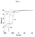
- FIG. 3 is a graph showing reflectance of each metal material according to a wavelength of light.
- reflectance of aluminum Al is higher than that of silver Ag in the range of a light wavelength of 500 nm or less.
- Inventors of the present invention have invented embodiments by taking accounting of unique characteristics of the above-mentioned metal material.
- each of the first organic light emitting layer OL1 and the second organic light emitting layer OL2 of each of the first organic light emitting element OLED1 and the second organic light emitting element OLED2 includes the same blue light emitting material, light emitted from each of the first organic light emitting layer OL1 and the second organic light emitting layer OL2 is the blue light having substantially the same wavelength.
- each of the first organic light emitting layer OL1 and the second organic light emitting layer OL2 has the same thickness, the first distance L1 between the first electrode E1 and the common electrode CE is equal to the second distance L2 between the second electrode E2 and the common electrode CE. Therefore, the blue light emitted from each of the first organic light emitting layer OL1 and the second organic light emitting layer OL2 needs to be reinforced to the same high purity blue light by the constructive interference between the first electrode E1 and the common electrode CE and between the second electrode E2 and the common electrode CE to be viewed to the outside through the common electrode CE.
- the first reflective layer RL1 of the first electrode E1 includes silver Ag having low reflectance at 500 nm or less and the second reflective layer RL2 of the second electrode E2 includes aluminum Al having high reflectance at 500 nm or less
- the first organic light emitting element OLED1 emits the first blue light, which is the sky blue light having the first wavelength of about 459 nm to about 490 nm
- the second organic light emitting element OLED2 emits the second blue light, which is the deep blue light having the second wavelength of about 440 nm to about 458 nm shorter than the first wavelength.
- the inventors of the present invention have performed an experiment in order to confirm those described above, and results of the above-mentioned experiment have been shown in FIG. 4 .
- FIG. 4 is a graph illustrating an effect of the organic light emitting diode display according to an embodiment of the invention.
- an x axis represents a wavelength of light and a y axis represents intensity of light.
- a hole injection layer PHIL of each of the first organic light emitting layer OL1 of the first organic light emitting element OLED1 and the second organic light emitting layer OL2 of the second organic light emitting element OLED2 has been formed to have substantially the same thickness of about 1155 ⁇
- the first reflective layer RL1 of the first electrode E1 of the first organic light emitting element OLED1 has been formed to include silver Ag having a thickness of about 1000 ⁇
- the second reflective layer RL2 of the second electrode E2 of the second organic light emitting element OLED2 has been formed to include aluminum Al having a thickness of about 1000 ⁇ .
- the first organic light emitting element OLED1 has emitted the sky blue light having a wavelength of 472 nm
- the second organic light emitting element OLED2 has emitted the deep blue light having a wavelength of 456 nm.
- each of the first organic light emitting layer OL1 of the first organic light emitting element OLED1 and the second organic light emitting layer OL2 of the second organic light emitting element OLED2 includes the same blue light emitting material and has the same thickness at the same time, since the first electrode E1 includes silver Ag having high reflectance and the second electrode E2 includes aluminum Al having higher reflectance for light having the second wavelength than silver Ag of the first electrode E1, the first organic light emitting element OLED1 emits the first blue light, which is the sky blue light having the first wavelength of 459nm to 490nm, and the second organic light emitting element OLED2 emits the second blue light, which is the deep blue light having the second wavelength of 440nm to 458nm shorter than the first wavelength.
- the second organic light emitting layer OL2 since the second organic light emitting layer OL2 has the same blue light emitting material as that of the first organic light emitting layer OL1 and has the same thickness as that of the first organic light emitting layer OL1 at the same time, the second organic light emitting layer OL2 may be formed simultaneously with the process of forming the first organic light emitting layer OL1. As a result, each of the first organic light emitting layer OL1 and the second organic light emitting layer OL2 may be simultaneously deposited on each of the first electrode E1 and the second electrode E2 by using one deposition process using one mask.
- the organic light emitting diode display 1000 includes the first organic light emitting element OLED1 and the second organic light emitting element OLED2 that emit different blue lights, it is possible to provide the organic light emitting diode display 1000 capable of reducing the manufacturing time and manufacturing costs.
- the organic light emitting diode display 1000 capable of improving light emission efficiency of each of a plurality of organic light emitting elements that emit lights having different wavelengths is provided.
- FIG. 5 is a cross-sectional view showing an organic light emitting diode display according to another embodiment of the invention.
- the second organic light emitting element OLED2 of the organic light emitting diode display 1000 emits the second blue light having the second wavelength which may be 440 nm to 458 nm shorter than the first blue light having the first wavelength which is emitted by the first organic light emitting element OLED1, and includes a second electrode E2, a second organic light emitting layer OL2, and a common electrode CE.
- the second electrode E2 includes a transparent oxide layer TO and a second reflective layer RL2.
- the second organic light emitting layer OL2 may contact the second reflective layer RL2.
- the second reflective layer RL2 includes aluminum Al, which is a metal having higher reflectance for the light having the second wavelength than the first electrode E1 of the first organic light emitting element OLED1.
- the second reflective layer RL2 reflects light emitted from the second organic light emitting layer OL2 in a direction of the common electrode CE.
- the second reflective layer RL2 of the second electrode E2 is formed of aluminum Al while the first reflective layer RL1 of the first electrode E1 is formed of silver Ag. Since the second electrode E2 includes the material different from that of the first electrode E1, the second electrode E2 may be formed by using an additional process after a process of forming the first electrode E1, but is not limited thereto.
- the second organic light emitting layer OL2 includes at least a main light emitting layer that emits light.
- the second organic light emitting layer OL2 may further include a hole injection layer, a hole transport layer, an auxiliary layer, an electronic transport layer, and an electronic injection layer.
- the second organic light emitting layer OL2 includes the same blue light emitting material as that of the first organic light emitting layer OL1.
- the second organic light emitting layer OL2 has substantially the same one thickness as that of the first organic light emitting layer OL1, and as a result, the second electrode E1 and the common electrode CE are spaced from each other with a second distance L2 substantially the same as the first distance L1.
- the second distance L2 may be an optimal distance at which constructive interference occurs in response to the blue light having the wavelength of 440 nm to 490 nm.
- the second organic light emitting layer OL2 since the second organic light emitting layer OL2 has the same blue light emitting material as that of the first organic light emitting layer OL1 and has the same thickness as that of the first organic light emitting layer OL1 at the same time, the second organic light emitting layer OL2 may be formed simultaneously with the process of forming the first organic light emitting layer OL1. Thereby, each of the first organic light emitting layer OL1 and the second organic light emitting layer OL2 may be simultaneously deposited on each of the first electrode E1 and the second electrode E2 by using one deposition process using one mask. This acts as a factor reducing time and costs for manufacturing the organic light emitting diode display.
- each of the first organic light emitting layer OL1 of the first organic light emitting element OLED1 and the second organic light emitting layer OL2 of the second organic light emitting element OLED2 includes the same blue light emitting material and has the same thickness at the same time, since the first electrode E1 includes silver Ag having high reflectance and the second electrode E2 includes aluminum Al having higher reflectance for light having the second wavelength than silver Ag of the first electrode E1, the first organic light emitting element OLED1 emits the first blue light, which is the sky blue light having the first wavelength of 459 nm to 490 nm, and the second organic light emitting element OLED2 emits the second blue light, which is the deep blue light having the second wavelength of 440 nm to 458 nm shorter than the first wavelength.
- the second organic light emitting layer OL2 since the second organic light emitting layer OL2 has the same blue light emitting material as that of the first organic light emitting layer OL1 and has the same thickness as that of the first organic light emitting layer OL1 at the same time, the second organic light emitting layer OL2 may be formed simultaneously with the process of forming the first organic light emitting layer OL1. As a result, each of the first organic light emitting layer OL1 and the second organic light emitting layer OL2 may be simultaneously deposited on each of the first electrode E1 and the second electrode E2 by using one deposition process using one mask.
- the organic light emitting diode display 1000 includes the first organic light emitting element OLED1 and the second organic light emitting element OLED2 that emit different blue lights, it is possible to provide the organic light emitting diode display 1000 capable of reducing the manufacturing time and manufacturing costs.
- the organic light emitting diode display 1000 capable of improving light emission efficiency of each of a plurality of organic light emitting elements that emit lights having different wavelengths is provided.
- FIG. 6 is a cross-sectional view showing an organic light emitting diode display according to another embodiment.
- the second organic light emitting element OLED2 of the organic light emitting diode display 1000 emits the second blue light having the second wavelength which may be 440 nm to 458 nm shorter than the first blue light having the first wavelength which is emitted by the first organic light emitting element OLED1, and includes a second electrode E2, a second organic light emitting layer OL2, and a common electrode CE.
- the second electrode E2 includes a transparent oxide layer TO, a second reflective layer RL2, and a second transparent conductive layer TL2.
- the second transparent conductive layer TL2 may be formed of a single layer or multilayer of light transmissive conductive material including one or more of indium tin oxide (ITO), amorphous indium tin oxide (a-ITO), indium zinc oxide (IZO), and the like, and may include a material having a high work function.
- the second transparent conductive layer TL2 includes a material which is different from that of the first transparent conductive layer TL1 of the first electrode E1.
- each of the first transparent conductive layer TL1 of the first organic light emitting element OLED1 and the second transparent conductive layer TL2 of the second organic light emitting element OLED2 includes different transparent conductive materials.
- the second transparent conductive layer TL2 of the second electrode E2 includes the transparent conductive material different from that of the first transparent conductive layer TL1 of the first electrode E1, it is possible to suppress the first transparent conductive layer TL1 from being etched by an etchant etching the second transparent conductive layer TL2, when the second electrode E2 is formed by using an additional process after the process of forming the first electrode E1.
- the organic light emitting diode display 1000 having improved reliability of the entire manufacturing process is provided.
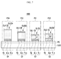
- FIG. 7 is a cross-sectional view showing an organic light emitting diode display according to another embodiment.
- the second reflective layer RL2 of the second electrode E2 of the second organic light emitting element OLED2 of an organic light emitting diode display 1000 has a thickness thicker than that of the first reflective layer RL1.
- the organic light emitting diode display 1000 having improved light emission efficiency of the second organic light emitting element OLED2 is provided.
- the first organic light emitting element OLED1 of an organic light emitting diode display 1000 emits the first blue light having the first wavelength which may be 459 nm to 490 nm, and includes the first electrode E1, the first organic light emitting layer OL1, and the common electrode CE.
- the first electrode E1 includes a transparent oxide layer TO, a first reflective layer RL1, and a first transparent conductive layer TL1.
- the first reflective layer RL1 includes silver Ag, which is a metal having high reflectance.
- the first reflective layer RL1 reflects light emitted from the first organic light emitting layer OL1 in a direction of the common electrode CE.
- the first transparent conductive layer TL1 may be formed of a single layer or multilayer of light transmissive conductive material including one or more of indium tin oxide (ITO), amorphous indium tin oxide (a-ITO), indium zinc oxide (IZO), and the like, and may include a material having a high work function.
- the first transparent conductive layer TL1 has a thickness substantially greater than that of the second transparent conductive layer TL2 of the second electrode E2 of the second organic light emitting element OLED2.
- the first organic light emitting layer OL1 includes at least a main light emitting layer that emits light.
- the first organic light emitting layer OL1 may further include a hole injection layer, a hole transport layer, an auxiliary layer, an electronic transport layer, and an electronic injection layer.
- the first organic light emitting layer OL1 includes a blue light emitting material.
- the first organic light emitting layer OL1 has a thickness which defines a first distance L1 between the first electrode E1 and the common electrode CE.
- the first reflective layer RL1 of the first electrode E1 and the common electrode CE have a third distance L3 therebetween.
- the third distance L3 may be an optimal distance at which constructive interference occurs in response to the first blue light having the first wavelength of 459 nm to 490 nm.
- the second organic light emitting element OLED2 may emit a second blue light having a second wavelength which may be 440 nm to 458 nm shorter than the first blue light having the first wavelength which is emitted by the first organic light emitting element OLED1, and include a second electrode E2, a second organic light emitting layer OL2, and a common electrode CE.
- the second electrode E2 includes a transparent oxide layer TO, a second reflective layer RL2, and a second transparent conductive layer TL2.
- the second reflective layer RL2 includes silver Ag, which is the same metal having high reflectance as that of the first electrode E1 of the first organic light emitting element OLED1.
- the second reflective layer RL2 reflects light emitted from the second organic light emitting layer OL2 in a direction of the common electrode CE.
- the second electrode E2 and the first electrode E1 include the same silver Ag
- the second electrode E2 includes the same material as that of the first electrode E1. Since the second electrode E2 includes the same material as that of the first electrode E1, the second electrode E2 may be formed simultaneously with the first electrode E1 by the process of forming the first electrode E1.
- the second transparent conductive layer TL2 may be formed of a single layer or multilayer of light transmissive conductive material including one or more of indium tin oxide (ITO), amorphous indium tin oxide (a-ITO), indium zinc oxide (IZO), and the like, and may include a material having a high work function.
- the second transparent conductive layer TL2 has a thickness substantially smaller than that of the first transparent conductive layer TL1 of the first electrode E1 of the first organic light emitting element OLED1.
- the second transparent conductive layer TL2 may be formed by using a half-tone mask or may be formed by using an additional deposition process.
- the second organic light emitting layer OL2 includes at least a main light emitting layer that emits light.
- the second organic light emitting layer OL2 may further include a hole injection layer, a hole transport layer, an auxiliary layer, an electronic transport layer, and an electronic injection layer.
- the second organic light emitting layer OL2 includes the same blue light emitting material as that of the first organic light emitting layer OL1.
- the second organic light emitting layer OL2 has substantially the same thickness as that of the first organic light emitting layer OL1, and as a result, the second electrode E2 and the common electrode CE are spaced from each other with a second distance L2 substantially the same as the first distance L1.
- the second reflective layer RL2 of the second electrode E2 and the common electrode CE have a fourth distance L4 substantially shorter than the third distance L3 therebetween.
- the fourth distance L4 may be an optimal distance at which constructive interference occurs in response to the second blue light having the second wavelength of 440 nm to 458 nm.
- each of the first organic light emitting layer OL1 of the first organic light emitting element OLED1 and the second organic light emitting layer OL2 of the second organic light emitting element OLED2 includes the same blue light emitting material and has the same thickness
- each of the first electrode E1 and the second electrode E2 includes the same material at the same time
- the second transparent conductive layer TL2 of the second electrode E2 has the thickness substantially smaller than that of the first transparent conductive layer TL1 of the first electrode E1
- the first reflective layer RL1 of the first organic light emitting element OLED1 and the common electrode CE have the third distance L3 therebetween
- the second reflective layer RL2 of the second organic light emitting element OLED2 and the common electrode CE have the fourth distance L4 therebetween.
- the blue light emitted from the first organic light emitting layer OL1 generates constructive interference corresponding to the first blue light having the first wavelength of 459 nm to 490 nm and the blue light emitted from the second organic light emitting layer OL2 generates constructive interference corresponding to the second blue light having the second wavelength of 440 nm to 458 nm
- the first organic light emitting element OLED1 emits the first blue light, which is the sky blue light having the first wavelength of 459 nm to 490 nm
- the second organic light emitting element OLED2 emits the second blue light, which is the deep blue light having the second wavelength of 440 nm to 458 nm shorter than the first wavelength.
- each of the first organic light emitting layer OL1 and the second organic light emitting layer OL2 of each of the first organic light emitting element OLED1 and the second organic light emitting element OLED2 has the same material and the same thickness
- resonance distances at which constructive interference of each of the first organic light emitting element OLED1 and the second organic light emitting element OLED2 occurs are set to be different from each other by forming the thickness of each of the first transparent conductive layer TL1 and the second transparent conductive layer TL2 to be different from each other.
- each of the first organic light emitting layer OL1 and the second organic light emitting layer OL2 is simultaneously formed by using one deposition process using one mask, each of the first organic light emitting element OLED1 and the second organic light emitting element OLED2 may be formed to emit different blue lights.
- the organic light emitting diode display 1000 includes the first organic light emitting element OLED1 and the second organic light emitting element OLED2 that emit different blue lights, it is possible to provide the organic light emitting diode display 1000 capable of reducing the manufacturing time and manufacturing costs.
- the organic light emitting diode display 1000 capable of improving light emission efficiency of each of a plurality of organic light emitting elements that emit lights having different wavelengths is provided.
Landscapes
- Physics & Mathematics (AREA)
- Optics & Photonics (AREA)
- Engineering & Computer Science (AREA)
- Manufacturing & Machinery (AREA)
- Electroluminescent Light Sources (AREA)
- Devices For Indicating Variable Information By Combining Individual Elements (AREA)
Abstract
Description
- The described technology relates generally to an organic light emitting diode display.
- A display device is a device displaying an image, and an organic light emitting diode display has been recently highlighted.
- Since the organic light emitting diode display has self-luminance characteristics and does not require a separate light source unlike a liquid crystal display device, a thickness and a weight thereof may be reduced. In addition, the organic light emitting diode display exhibits high quality characteristics such as reduced consumption power, increased luminance, fast response speed, and the like.
- In general, the organic light emitting diode display includes an array of organic light emitting elements that emit light having different wavelengths per a pixel, which is a minimum unit displaying the image. The above-mentioned organic light emitting element includes a first electrode, an organic layer emitting light, and a second electrode which are sequentially stacked, wherein the organic layer is deposited on the first electrode using a mask.
- The above information disclosed in this Background section is only for enhancement of understanding of the background of the described technology and therefore it may contain information that does not form the prior art that is already known in this country to a person of ordinary skill in the art.
- The described technology provides an organic light emitting diode display having advantages of improving light emission efficiency of each of a plurality of organic light emitting elements that emit lights having different wavelengths, even though the number of masks used for depositing an organic layer is not increased.
- One aspect of the invention provides an organic light emitting diode display device, which may comprise: a first organic light emitting element configured to emit light having a first wavelength; and a second organic light emitting element configured to emit light having a second wavelength substantially shorter than the first wavelength, wherein the first organic light emitting element comprises a first electrode, and wherein the second organic light emitting element comprises a second electrode having substantially higher reflectance for the light having the second wavelength than the first electrode.
- In the foregoing device, the first and second electrodes may comprise first and second reflective layers, respectively, wherein the second reflective layer of the second electrode is formed of a material different from that of the first reflective layer of the first electrode. The first organic light emitting element and the second organic light emitting element may respectively comprise first and second organic light emitting layers that are formed of the same material and have substantially the same thickness, the first and second organic light emitting layers being disposed over the first electrode and the second electrode, respectively. The first and second organic light emitting layers may comprise a blue light emitting material. The first organic light emitting element and the second organic light emitting element may further comprise a common electrode disposed over the first and second organic light emitting layers, wherein a first distance between the first electrode and the common electrode may be substantially the same as a second distance between the second electrode and the common electrode.
- Still in the foregoing device, the first reflective layer of the first electrode may comprise silver (Ag), and the second reflective layer of the second electrode may comprise aluminum (Al). The first electrode may comprise a first transparent conductive layer disposed over the first reflective layer, and wherein the second electrode does not comprise an intervening transparent conductive layer between the second reflective layer and the second organic light emitting layer. The first electrode comprises a first transparent conductive layer disposed over the first reflective layer, and wherein the second electrode may further comprise a second transparent conductive layer disposed over the second reflective layer. The first transparent conductive layer and the second transparent conductive layer may comprise different transparent conductive materials. A thickness of the second reflective layer may be substantially greater than that of the first reflective layer.
- Yet in the foregoing device, the light having the first wavelength and the light having the second wavelength may be blue light. The first wavelength may be about 459 nm to about 490 nm, and the second wavelength may be about 440 nm to about 458 nm. The first organic light emitting element may further comprise: a first organic light emitting layer disposed over the first electrode; and a common electrode disposed over the first organic light emitting layer, wherein the second organic light emitting element may further comprise: a second organic light emitting layer disposed over the second electrode; and the common electrode disposed over the second organic light emitting layer. The first organic light emitting layer and the second organic light emitting layer may be formed of the same material and have substantially the same thickness. A distance between the first electrode and the common electrode may be substantially the same as a distance between the second electrode and the common electrode. The organic light emitting diode display device may further comprise: a third organic light emitting element configured to emit light having a third wavelength longer than the first wavelength; and a fourth organic light emitting element configured to emit light having a fourth wavelength longer than the third wavelength. The third organic light emitting element and the fourth organic light emitting element may respectively comprise third and fourth organic light emitting layers having thicknesses different from each other.
- Another aspect of the invention provides an organic light emitting diode display device, which may comprise: a first organic light emitting element configured to emit light having a first wavelength; and a second organic light emitting element configured to emit light having a second wavelength substantially shorter than the first wavelength, wherein the first organic light emitting element comprises a first reflective layer and a first electrode that comprises a first transparent conductive layer and is disposed over the first reflective layer, and wherein the second organic light emitting element comprises a second reflective layer and a second electrode that is disposed over the second reflective layer and comprises a second transparent conductive layer having a thickness substantially smaller than that of the first transparent conductive layer.
- In the foregoing device, the first reflective layer and the second reflective layer may be formed of the same material. The first organic light emitting element and the second organic light emitting element may respectively comprise first and second organic light emitting layers that are formed of the same material and have substantially the same thickness, the first and second organic light emitting layers being disposed over the first electrode and the second electrode, respectively.
- An embodiment provides an organic light emitting diode display including: a first organic light emitting element emitting light having a first wavelength; and a second organic light emitting element emitting light having a second wavelength shorter than the first wavelength, wherein the first organic light emitting element includes a first electrode, and the second organic light emitting element includes a second electrode having higher reflectance for the light having the second wavelength than the first electrode.
- The second electrode may include a material different from that of the first electrode.
- Each of the first organic light emitting element and the second organic light emitting element may further include the same organic light emitting layer having the same thickness disposed on each of the first electrode and the second electrode.
- The organic light emitting layer may include a blue light emitting material. Each of the first organic light emitting element and the second organic light emitting element may further include a common electrode disposed on the organic light emitting layer, and a distance between the first electrode and the common electrode, and a distance between the second electrode and the common electrode may be the same as each other
- The first electrode may include silver Ag, and the second electrode may include aluminum Al.
- The first electrode may include a first reflective layer including silver Ag, and a first transparent conductive layer disposed on the first reflective layer, and the second electrode may include a second reflective layer including aluminum Al.
- The second electrode may further include a second transparent conductive layer disposed on the second reflective layer.
- Each of the first transparent conductive layer and the second transparent conductive layer may include different transparent conductive materials.
- A thickness of the second reflective layer may be thicker than that of the first reflective layer.
- The light having the first wavelength and the light having the second wavelength may be blue lights different from each other.
- The first wavelength may be 459 nm to 490 nm, and the second wavelength may be 440 nm to 458 nm.
- The first organic light emitting element may further include: a first organic light emitting layer disposed on the first electrode; and a common electrode disposed on the first organic light emitting layer, and the second organic light emitting element may further include: a second organic light emitting layer disposed on the second electrode; and the common electrode disposed on the second organic light emitting layer.
- Each of the first organic light emitting layer and the second organic light emitting layer may be the same organic layer having the same thickness.
- A distance between the first electrode and the common electrode may be the same as a distance between the second electrode and the common electrode.
- The organic light emitting diode display may further include a third organic light emitting element emitting light having a third wavelength longer than the first wavelength; and a fourth organic light emitting element emitting light having a fourth wavelength longer than the third wavelength.
- The third organic light emitting element and the fourth organic light emitting element may include different organic light emitting layers having thicknesses different from each other.
- Another embodiment provides an organic light emitting diode display including: a first organic light emitting element emitting light having a first wavelength; and a second organic light emitting element emitting light having a second wavelength shorter than the first wavelength, wherein the first organic light emitting element includes a first reflective layer and a first electrode including a first transparent conductive layer disposed on the first reflective layer, and the second organic light emitting element includes a second reflective layer and a second electrode disposed on the second reflective layer and including a second transparent conductive layer having a thickness thinner than that of the first transparent conductive layer.
- The first reflective layer may include the same material as that of the second reflective layer.
- Each of the first organic light emitting element and the second organic light emitting element may further include the same organic light emitting layer having the same thickness disposed on each of the first electrode and the second electrode.
- At least some of the above and other features of the invention are set out in the claims.
- According to an embodiment of the invention, even though the number of masks used for depositing the organic layer is not increased, the organic light emitting diode display capable of improving light emission efficiency of each of the plurality of organic light emitting elements that emit lights having different wavelengths may be provided.
-
-
FIG. 1 is a plan view showing pixels of an organic light emitting diode display according to an embodiment of the invention. -
FIG. 2 is a cross-sectional view taken along a line II - II ofFIG. 1 . -
FIG. 3 is a graph showing reflectance of each metal material according to a wavelength of light. -
FIG. 4 is a graph illustrating an effect of the organic light emitting diode display according to an embodiment of the invention. -
FIG. 5 is a cross-sectional view showing an organic light emitting diode display according to another embodiment of the invention. -
FIG. 6 is a cross-sectional view showing an organic light emitting diode display according to another embodiment of the invention. -
FIG. 7 is a cross-sectional view showing an organic light emitting diode display according to another embodiment of the invention. -
FIG. 8 is a cross-sectional view showing an organic light emitting diode display according to another embodiment of the invention. - Hereinafter, embodiments of the invention will be described in detail with reference to the accompanying drawings so that those skilled in the art may easily practice the present invention. The present invention may be implemented in various different forms and is not limited to the embodiments described in the present specification.
- Accordingly, the drawings and description are to be regarded as illustrative in nature and not restrictive. Like reference numerals designate like elements throughout the specification.
- In several embodiments, components having the same configuration will be described representatively in an embodiment by the same reference numerals. In embodiments other than an embodiment, configurations different from those of an embodiment will be described.
- In addition, since sizes and thicknesses of the respective components shown in the drawings are arbitrarily shown for the convenience of explanation, the present invention is not necessarily limited to those shown in the drawings.
- In the drawings, the thickness of layers, films, panels, regions, etc., are exaggerated for clarity. In addition, in the drawings, thicknesses of some layers and regions are exaggerated for convenience of explanation. It will be understood that when an element such as a layer, film, region, or substrate is referred to as being "on" another element, it can be directly on the other element or intervening elements may also be present.
- In addition, unless explicitly described to the contrary, the word "comprise" and variations such as "comprises" or "comprising", will be understood to imply the inclusion of stated elements but not the exclusion of any other elements. In addition, throughout the specification, when an element is referred to as being "on" another element, it means that the element is positioned on or below of a target portion, and does not necessarily mean that the element is positioned at an upper side based on a gravity direction.
- Hereinafter, an organic light emitting diode display according to an embodiment will be described with reference to
FIGS. 1 and2 . -
FIG. 1 is a plan view showing pixels of an organic light emitting diode display according to an embodiment of the invention. - As shown in
FIG. 1 , an organic light emittingdiode display 1000 according to an embodiment includes a first pixel PX1, a second pixel PX2, a third pixel PX3, and a fourth pixel PX4. The pixel means a smallest unit displaying an image. In embodiments, each of the first pixel PX1, the second pixel PX2, the third pixel PX3, and the fourth pixel PX4 may be referred to as a sub-pixel, and these subpixels (the first pixel PX1, the second pixel PX2, the third pixel PX3, and the fourth pixel PX4 described above) may constitute one single pixel which is included in an array of pixels, but is not limited thereto. In embodiments, the first pixel PX1, the second pixel PX2, the third pixel PX3, and the fourth pixel PX4 may respectively constitute one single pixel. Alternatively, two or three of the first pixel PX1, the second pixel PX2, the third pixel PX3, and the fourth pixel PX4 may constitute one single pixel. - The first pixel PX1 emits a first blue light and includes a first organic light emitting element and a pixel circuit connected to the first organic light emitting element. Here, the first blue light may be sky blue light having a first wavelength of 459 nm to 490 nm, but is not limited thereto.
- The second pixel PX2 emits a second blue light and includes a second organic light emitting element and a pixel circuit connected to the second organic light emitting element. Here, the second blue light may be deep blue light having a second wavelength of 440 nm to 458 nm, but is not limited thereto.
- The third pixel PX3 emits green light having a third wavelength and includes a third organic light emitting element and a pixel circuit connected to the third organic light emitting element.
- The fourth pixel PX4 emits red light having a fourth wavelength and includes a fourth organic light emitting element and a pixel circuit connected to the fourth organic light emitting element.
-
FIG. 2 is a cross-sectional view taken along a line II - II ofFIG. 1 . - As shown in
FIG. 2 , the first pixel PX1 includes a first organic light emitting element OLED1 and a pixel circuit PC formed on a substrate SUB connected to the first organic light emitting element OLED1. In embodiments, the substrate SUB may be flexible, stretchable, foldable, bendable, or rollable, but is not limited thereto. The substrate SUB is flexible, stretchable, foldable, bendable, or rollable, such that the entire organic light emittingdiode display 1000 may be flexible, stretchable, foldable, bendable, or rollable. In alternative embodiments, the substrate may be rigid or non-flexible. - In addition, the pixel circuit PC may include a wiring structure, transistors and at least one capacitor that are disposed on the substrate SUB. The wiring structure includes electrically conductive lines including one or more scan lines, data lines, driving power lines, common power lines, and the like. The two or more thin film transistors TFTs connected to the lines may be provided for one organic light emitting element. The pixel circuit PC may have various known structures.
- The first organic light emitting element OLED1 may emit a first blue light having a first wavelength which may be about 459 nm to about 490 nm, and include a first electrode E1, a first organic light emitting layer OL1, and a common electrode CE.
- The first electrode E1 may be an anode which is connected to the pixel circuit PC and which is a hole injection electrode, but is not limited thereto. Alternatively, the first electrode E1 may be a cathode, which is an electron injection electrode. The first electrode E1 includes a transparent oxide layer TO, a first reflective layer RL1, and a first transparent conductive layer TL1.
- The transparent oxide layer TO may be formed of a single layer or multilayer of light transmissive conductive material including one or more of indium tin oxide (ITO), indium zinc oxide (IZO), and the like.
- The first reflective layer RL1 includes silver Ag, which is a metal having high reflectance. The first reflective layer RL1 reflects light emitted from the first organic light emitting layer OL1 in a direction of the common electrode CE.
- The first transparent conductive layer TL1 may be formed of a single layer or multilayer of light transmissive conductive material including one or more of indium tin oxide (ITO), amorphous indium tin oxide (a-ITO), indium zinc oxide (IZO), and the like, and may include a material having a high work function.
- The first organic light emitting layer OL1 includes at least a main light emitting layer that emits light. In embodiments, the first organic light emitting layer OL1 may further include a hole injection layer, a hole transport layer, an auxiliary layer, an electronic transport layer, and an electronic injection layer. The first organic light emitting layer OL1 includes a blue light emitting material. In embodiments, the first organic light emitting layer OL1 has a thickness which defines a first distance L1 between the first electrode E1 and the common electrode CE. In embodiments, the first distance L1 may be an optimal distance at which constructive interference occurs in response to the blue light having the wavelength of about 440 nm to about 490 nm.
- The common electrode CE may be the cathode, which is the electron injection electrode, but is not limited thereto. In alternative embodiments, the common electrode CE may be the anode, which is the hole injection electrode. The common electrode CE may have a shape which is extended throughout the first organic light emitting element OLED1, a second organic light emitting element OLED2, a third organic light emitting element OLED3, and a fourth organic light emitting element OLED4. The common electrode CE may include a single layer or multilayer of light transmissive conductive material or a light semi-transmissive conductive material including one or more of indium tin oxide (ITO), indium zinc oxide (IZO), aluminum Al, silver Ag, and the like.
- The second pixel PX2 includes the second organic light emitting element OLED2 and a pixel circuit PC formed on the substrate SUB connected to the second organic light emitting element OLED2.
- The second organic light emitting element OLED2 may emit a second blue light having a second wavelength which may be about 440 nm to about 458 nm shorter than the first blue light having the first wavelength which is emitted by the first organic light emitting element OLED1, and include a second electrode E2, a second organic light emitting layer OL2, and a common electrode CE.
- In embodiments, the second blue light having the second wavelength which is emitted by the second organic light emitting element OLED2 is blue light different from the first blue light having the first wavelength which is emitted by the first organic light emitting element OLED1.
- The second electrode E2 may be the anode which is connected to the pixel circuit PC and which is the hole injection electrode, but is not limited thereto. In alternative embodiments, the second electrode E2 may be the cathode, which is the electron injection electrode. The second electrode E2 includes a transparent oxide layer TO, a second reflective layer RL2, and a second transparent conductive layer TL2.
- The transparent oxide layer TO may be formed of a single layer or multilayer of light transmissive conductive material including one or more of indium tin oxide (ITO), indium zinc oxide (IZO), and the like.
- The second reflective layer RL2 includes aluminum Al, which is a metal having higher reflectance for the light having the second wavelength than the first electrode E1 of the first organic light emitting element OLED1. The second reflective layer RL2 reflects light emitted from the second organic light emitting layer OL2 in a direction of the common electrode CE.
- In embodiments, the second reflective layer RL2 of the second electrode E2 is formed of a material different material from that of the first reflective layer RL1 of the first electrode E1. In one embodiment, the second reflective layer RL2 is formed of aluminum Al while the first reflective layer RL1 is formed of silver Ag. Since the second electrode E2 includes the material different from that of the first electrode E1, the second electrode E2 may be formed by using an additional process after a process of forming the first electrode E1, but is not limited thereto.
- The second transparent conductive layer TL2 may be formed of a single layer or multilayer of light transmissive conductive material including one or more of indium tin oxide (ITO), amorphous indium tin oxide (a-ITO), indium zinc oxide (IZO), and the like, and may include a material having a high work function. The second transparent conductive layer TL2 may include the same material as that of the first transparent conductive layer TL1 of the first electrode E1, but is not limited thereto. Alternatively, the second transparent conductive layer TL2 may include a material different from that of the first transparent conductive layer TL1.
- The second organic light emitting layer OL2 includes at least a main light emitting layer that emits light. In embodiments, the second organic light emitting layer OL2 may further include a hole injection layer, a hole transport layer, an auxiliary layer, an electronic transport layer, and an electronic injection layer. The second organic light emitting layer OL2 includes the same blue light emitting material as that of the first organic light emitting layer OL1. The second organic light emitting layer OL2 has substantially the same thickness as that of the first organic light emitting layer OL1, and as a result, the second electrode E2 and the common electrode CE are spaced from each other with a second distance L2 substantially the same as the first distance L1. Here, the second distance L2 may be an optimal distance at which constructive interference occurs in response to the blue light having the wavelength of about 440 nm to about 490 nm.
- In embodiments, since the second organic light emitting layer OL2 has the same blue light emitting material as that of the first organic light emitting layer OL1 and has the same thickness as that of the first organic light emitting layer OL1 at the same time, the second organic light emitting layer OL2 may be formed simultaneously with the process of forming the first organic light emitting layer OL1. Thereby, each of the first organic light emitting layer OL1 and the second organic light emitting layer OL2 may be simultaneously deposited on each of the first electrode E1 and the second electrode E2 by using one deposition process using one mask. This acts as a factor reducing time and costs for manufacturing the organic light emitting diode display.
- The common electrode CE may be the cathode, which is the electron injection electrode, but is not limited thereto. In alternative embodiments, the common electrode CE may be the anode, which is the hole injection electrode. The common electrode CE may have a shape which is extended throughout the first organic light emitting element OLED1, the second organic light emitting element OLED2, the third organic light emitting element OLED3, and the fourth organic light emitting element OLED4. The common electrode CE may include a single layer or multilayer of light transmissive conductive material or a light semi-transmissive conductive material including one or more of indium tin oxide (ITO), indium zinc oxide (IZO), aluminum Al, silver Ag, and the like.
- The third pixel PX3 includes the third organic light emitting element OLED3 and a pixel circuit PC formed on the substrate SUB connected to the third organic light emitting element OLED3.
- The third organic light emitting element OLED3 emits green light having a third wavelength longer than the first wavelength, and includes a third electrode E3, a third organic light emitting layer OL3, and a common electrode CE.
- The third electrode E3 may be the anode which is connected to the pixel circuit PC and which is the hole injection electrode, but is not limited thereto. In alternative embodiments, the third electrode E3 may be the cathode, which is the electron injection electrode. The third electrode E3 includes a transparent oxide layer TO, a third reflective layer RL3, and a third transparent conductive layer TL3.
- The transparent oxide layer TO may be formed of a single layer or multilayer of light transmissive conductive material including one or more of indium tin oxide (ITO), indium zinc oxide (IZO), and the like.
- The third reflective layer RL3 may include silver Ag, which is the same metal as that of the first reflective layer RL1 of the first electrode E1, but is not limited thereto. In alternative embodiments, the third reflective layer RL3 may include one or more of silver Ag and aluminum Al. The third reflective layer RL3 reflects light emitted from the third organic light emitting layer OL3 in a direction of the common electrode CE.
- In embodiments, the third reflective layer RL3 of the third electrode E3 is formed of a material the same as that of the first reflect layer RL1 of the first electrode E1. Since the third electrode E3 includes the same material as that of the first electrode E1, the third electrode E3 may be formed simultaneously with the first electrode E1 by the process of forming the first electrode E1.
- In alternative embodiments, the third reflective layer RL3 of the third electrode E3 is formed of a material the same as that of the second reflective layer RL2 of the second electrode E2. Since the third electrode E3 includes the same material as that of the second electrode E2, the third electrode E3 may be formed simultaneously with the second electrode E2 by the process of forming the second electrode E2, but is not limited thereto.
- The third transparent conductive layer TL3 may be formed of a single layer or multilayer of light transmissive conductive material including one or more of indium tin oxide (ITO), amorphous indium tin oxide (a-ITO), indium zinc oxide (IZO), and the like, and may include a material having a high work function. The third transparent conductive layer TL3 may include the same material as that of the first transparent conductive layer TL1 of the first electrode E1.
- The third organic light emitting layer OL3 includes at least a main light emitting layer that emits light. In embodiments, the third organic light emitting layer OL3 may further include a hole injection layer, a hole transport layer, an auxiliary layer, an electronic transport layer, and an electronic injection layer. The third organic light emitting layer OL3 includes a green light emitting material. The third organic light emitting layer OL3 has a thickness substantially greater than that of the first organic light emitting layer OL1, and as a result, the third electrode E3 and the common electrode CE are spaced from each other with a distance longer than the first distance L1. Here, the distance between the third electrode E3 and the common electrode CE may be an optimal distance at which constructive interference occurs in response to the green light.
- The common electrode CE may be the cathode, which is the electron injection electrode, but is not limited thereto. In alternative embodiments, the common electrode CE may be the anode, which is the hole injection electrode.
- The fourth pixel PX4 includes the fourth organic light emitting element OLED4 and a pixel circuit PC formed on the substrate SUB connected to the fourth organic light emitting element OLED4.
- The fourth organic light emitting element OLED4 emits red light having a fourth wavelength longer than the third wavelength, and includes a fourth electrode E4, a fourth organic light emitting layer OL4, and a common electrode CE.
- The fourth electrode E4 may be the anode which is connected to the pixel circuit PC and which is the hole injection electrode, but is not limited thereto. In alternative embodiments, the fourth electrode E4 may be the cathode, which is the electron injection electrode. The fourth electrode E4 includes a transparent oxide layer TO, a fourth reflective layer RL4, and a fourth transparent conductive layer TL4.
- The transparent oxide layer TO may be formed of a single layer or multilayer of light transmissive conductive material including one or more of indium tin oxide (ITO), indium zinc oxide (IZO), and the like.
- The fourth reflective layer RL4 may include silver Ag, which is the same metal as that of the first reflective layer RL1 of the first electrode E1, but is not limited thereto. In alternative embodiments, the fourth reflective layer RL4 may include one or more of silver Ag and aluminum Al. The fourth reflective layer RL4 reflects light emitted from the fourth organic light emitting layer OL4 in a direction of the common electrode CE.
- In embodiments, the fourth reflective layer RL4 of the fourth electrode E4 is formed of a material the same as that of the first reflective layer RL1 of the first electrode E1. Since the fourth electrode E4 includes the same material as that of the first electrode E1, the fourth electrode E4 may be formed simultaneously with the first electrode E1 by the process of forming the first electrode E1.
- In alternative embodiments, the fourth reflective layer RL4 of the fourth electrode E4 is formed of a material the same as that of the second reflective layer RL2 of the second electrode E2. Since the fourth electrode E4 includes the same material as that of the second electrode E2, the fourth electrode E4 may be formed simultaneously with the second electrode E2 by the process of forming the second electrode E2, but is not limited thereto.
- The fourth transparent conductive layer TL4 may be formed of a single layer or multilayer of light transmissive conductive material including one or more of indium tin oxide (ITO), amorphous indium tin oxide (a-ITO), indium zinc oxide (IZO), and the like, and may include a material having a high work function. The fourth transparent conductive layer TL4 may include the same material as that of the first transparent conductive layer TL1 of the first electrode E1.
- The fourth organic light emitting layer OL4 includes at least a main light emitting layer that emits light. In embodiments, the fourth organic light emitting layer OL4 may further include a hole injection layer, a hole transport layer, an auxiliary layer, an electronic transport layer, and an electronic injection layer. The fourth organic light emitting layer OL4 includes a red light emitting material. The fourth organic light emitting layer OL4 has a thickness substantially greater than that of the third organic light emitting layer OL3, and as a result, the fourth electrode E4 and the common electrode CE are spaced from each other with a distance longer than the distance between the third electrode E3 and the common electrode CE. Here, the distance between the fourth electrode E4 and the common electrode CE may be an optimal distance at which constructive interference occurs in response to the red light.
- The common electrode CE may be the cathode, which is the electron injection electrode, but is not limited thereto. In alternative embodiments, the common electrode CE may be the anode, which is the hole injection electrode.
- Hereinafter, an effect of the organic light emitting diode display according to an embodiment described above will be described with reference to
FIGS. 3 and4 . -
FIG. 3 is a graph showing reflectance of each metal material according to a wavelength of light. - As shown in
FIG. 3 , it may be seen that reflectance of aluminum Al is higher than that of silver Ag in the range of a light wavelength of 500 nm or less. Inventors of the present invention have invented embodiments by taking accounting of unique characteristics of the above-mentioned metal material. - Since each of the first organic light emitting layer OL1 and the second organic light emitting layer OL2 of each of the first organic light emitting element OLED1 and the second organic light emitting element OLED2 includes the same blue light emitting material, light emitted from each of the first organic light emitting layer OL1 and the second organic light emitting layer OL2 is the blue light having substantially the same wavelength.
- In addition, since each of the first organic light emitting layer OL1 and the second organic light emitting layer OL2 has the same thickness, the first distance L1 between the first electrode E1 and the common electrode CE is equal to the second distance L2 between the second electrode E2 and the common electrode CE. Therefore, the blue light emitted from each of the first organic light emitting layer OL1 and the second organic light emitting layer OL2 needs to be reinforced to the same high purity blue light by the constructive interference between the first electrode E1 and the common electrode CE and between the second electrode E2 and the common electrode CE to be viewed to the outside through the common electrode CE. However, since the first reflective layer RL1 of the first electrode E1 includes silver Ag having low reflectance at 500 nm or less and the second reflective layer RL2 of the second electrode E2 includes aluminum Al having high reflectance at 500 nm or less, the first organic light emitting element OLED1 emits the first blue light, which is the sky blue light having the first wavelength of about 459 nm to about 490 nm, and the second organic light emitting element OLED2 emits the second blue light, which is the deep blue light having the second wavelength of about 440 nm to about 458 nm shorter than the first wavelength.
- The inventors of the present invention have performed an experiment in order to confirm those described above, and results of the above-mentioned experiment have been shown in
FIG. 4 . -
FIG. 4 is a graph illustrating an effect of the organic light emitting diode display according to an embodiment of the invention. In the graph ofFIG. 4 , an x axis represents a wavelength of light and a y axis represents intensity of light. - As shown in
FIG. 4 , a hole injection layer PHIL of each of the first organic light emitting layer OL1 of the first organic light emitting element OLED1 and the second organic light emitting layer OL2 of the second organic light emitting element OLED2 has been formed to have substantially the same thickness of about 1155 Å, the first reflective layer RL1 of the first electrode E1 of the first organic light emitting element OLED1 has been formed to include silver Ag having a thickness of about 1000 Å, and the second reflective layer RL2 of the second electrode E2 of the second organic light emitting element OLED2 has been formed to include aluminum Al having a thickness of about 1000 Å. As a result, the first organic light emitting element OLED1 has emitted the sky blue light having a wavelength of 472 nm, and the second organic light emitting element OLED2 has emitted the deep blue light having a wavelength of 456 nm. - As such, in the organic light emitting
diode display 1000 according to an embodiment, even though each of the first organic light emitting layer OL1 of the first organic light emitting element OLED1 and the second organic light emitting layer OL2 of the second organic light emitting element OLED2 includes the same blue light emitting material and has the same thickness at the same time, since the first electrode E1 includes silver Ag having high reflectance and the second electrode E2 includes aluminum Al having higher reflectance for light having the second wavelength than silver Ag of the first electrode E1, the first organic light emitting element OLED1 emits the first blue light, which is the sky blue light having the first wavelength of 459nm to 490nm, and the second organic light emitting element OLED2 emits the second blue light, which is the deep blue light having the second wavelength of 440nm to 458nm shorter than the first wavelength. - In embodiments of the invention, since the second organic light emitting layer OL2 has the same blue light emitting material as that of the first organic light emitting layer OL1 and has the same thickness as that of the first organic light emitting layer OL1 at the same time, the second organic light emitting layer OL2 may be formed simultaneously with the process of forming the first organic light emitting layer OL1. As a result, each of the first organic light emitting layer OL1 and the second organic light emitting layer OL2 may be simultaneously deposited on each of the first electrode E1 and the second electrode E2 by using one deposition process using one mask.
- Since this acts as a factor reducing total manufacturing time and manufacturing costs of the organic light emitting diode display, even though the organic light emitting
diode display 1000 includes the first organic light emitting element OLED1 and the second organic light emitting element OLED2 that emit different blue lights, it is possible to provide the organic light emittingdiode display 1000 capable of reducing the manufacturing time and manufacturing costs. - In short, even though the number of masks used for depositing the organic light emitting layer is not increased, the organic light emitting
diode display 1000 capable of improving light emission efficiency of each of a plurality of organic light emitting elements that emit lights having different wavelengths is provided. - Hereinafter, an organic light emitting diode display according to another embodiment will be described with reference to
FIG 5 . Portions which are different from the organic light emitting diode display according to an embodiment described above will be described. -
FIG. 5 is a cross-sectional view showing an organic light emitting diode display according to another embodiment of the invention. - As shown in
FIG. 5 , the second organic light emitting element OLED2 of the organic light emittingdiode display 1000 according to this embodiment emits the second blue light having the second wavelength which may be 440 nm to 458 nm shorter than the first blue light having the first wavelength which is emitted by the first organic light emitting element OLED1, and includes a second electrode E2, a second organic light emitting layer OL2, and a common electrode CE. - The second electrode E2 includes a transparent oxide layer TO and a second reflective layer RL2. In embodiments, the second organic light emitting layer OL2 may contact the second reflective layer RL2.
- The second reflective layer RL2 includes aluminum Al, which is a metal having higher reflectance for the light having the second wavelength than the first electrode E1 of the first organic light emitting element OLED1. The second reflective layer RL2 reflects light emitted from the second organic light emitting layer OL2 in a direction of the common electrode CE.
- In embodiments, the second reflective layer RL2 of the second electrode E2 is formed of aluminum Al while the first reflective layer RL1 of the first electrode E1 is formed of silver Ag. Since the second electrode E2 includes the material different from that of the first electrode E1, the second electrode E2 may be formed by using an additional process after a process of forming the first electrode E1, but is not limited thereto.
- The second organic light emitting layer OL2 includes at least a main light emitting layer that emits light. In embodiments, the second organic light emitting layer OL2 may further include a hole injection layer, a hole transport layer, an auxiliary layer, an electronic transport layer, and an electronic injection layer. The second organic light emitting layer OL2 includes the same blue light emitting material as that of the first organic light emitting layer OL1. The second organic light emitting layer OL2 has substantially the same one thickness as that of the first organic light emitting layer OL1, and as a result, the second electrode E1 and the common electrode CE are spaced from each other with a second distance L2 substantially the same as the first distance L1. Here, the second distance L2 may be an optimal distance at which constructive interference occurs in response to the blue light having the wavelength of 440 nm to 490 nm.
- In embodiments, since the second organic light emitting layer OL2 has the same blue light emitting material as that of the first organic light emitting layer OL1 and has the same thickness as that of the first organic light emitting layer OL1 at the same time, the second organic light emitting layer OL2 may be formed simultaneously with the process of forming the first organic light emitting layer OL1. Thereby, each of the first organic light emitting layer OL1 and the second organic light emitting layer OL2 may be simultaneously deposited on each of the first electrode E1 and the second electrode E2 by using one deposition process using one mask. This acts as a factor reducing time and costs for manufacturing the organic light emitting diode display.
- As such, in the organic light emitting
diode display 1000 according to another embodiment, even though each of the first organic light emitting layer OL1 of the first organic light emitting element OLED1 and the second organic light emitting layer OL2 of the second organic light emitting element OLED2 includes the same blue light emitting material and has the same thickness at the same time, since the first electrode E1 includes silver Ag having high reflectance and the second electrode E2 includes aluminum Al having higher reflectance for light having the second wavelength than silver Ag of the first electrode E1, the first organic light emitting element OLED1 emits the first blue light, which is the sky blue light having the first wavelength of 459 nm to 490 nm, and the second organic light emitting element OLED2 emits the second blue light, which is the deep blue light having the second wavelength of 440 nm to 458 nm shorter than the first wavelength. - In embodiments, since the second organic light emitting layer OL2 has the same blue light emitting material as that of the first organic light emitting layer OL1 and has the same thickness as that of the first organic light emitting layer OL1 at the same time, the second organic light emitting layer OL2 may be formed simultaneously with the process of forming the first organic light emitting layer OL1. As a result, each of the first organic light emitting layer OL1 and the second organic light emitting layer OL2 may be simultaneously deposited on each of the first electrode E1 and the second electrode E2 by using one deposition process using one mask.
- Since this acts as a factor reducing total manufacturing time and manufacturing costs of the organic light emitting diode display, even though the organic light emitting
diode display 1000 includes the first organic light emitting element OLED1 and the second organic light emitting element OLED2 that emit different blue lights, it is possible to provide the organic light emittingdiode display 1000 capable of reducing the manufacturing time and manufacturing costs. - In short, even though the number of masks used for depositing the organic light emitting layer is not increased, the organic light emitting
diode display 1000 capable of improving light emission efficiency of each of a plurality of organic light emitting elements that emit lights having different wavelengths is provided. - Hereinafter, an organic light emitting diode display according to another embodiment will be described with reference to
FIG 6 . Portions which are different from the organic light emitting diode display according to an embodiment described above will be described. -
FIG. 6 is a cross-sectional view showing an organic light emitting diode display according to another embodiment. - As shown in
FIG. 6 , the second organic light emitting element OLED2 of the organic light emittingdiode display 1000 according to another embodiment emits the second blue light having the second wavelength which may be 440 nm to 458 nm shorter than the first blue light having the first wavelength which is emitted by the first organic light emitting element OLED1, and includes a second electrode E2, a second organic light emitting layer OL2, and a common electrode CE. - The second electrode E2 includes a transparent oxide layer TO, a second reflective layer RL2, and a second transparent conductive layer TL2.
- The second transparent conductive layer TL2 may be formed of a single layer or multilayer of light transmissive conductive material including one or more of indium tin oxide (ITO), amorphous indium tin oxide (a-ITO), indium zinc oxide (IZO), and the like, and may include a material having a high work function. The second transparent conductive layer TL2 includes a material which is different from that of the first transparent conductive layer TL1 of the first electrode E1. In embodiments, each of the first transparent conductive layer TL1 of the first organic light emitting element OLED1 and the second transparent conductive layer TL2 of the second organic light emitting element OLED2 includes different transparent conductive materials.
- As such, since the second transparent conductive layer TL2 of the second electrode E2 includes the transparent conductive material different from that of the first transparent conductive layer TL1 of the first electrode E1, it is possible to suppress the first transparent conductive layer TL1 from being etched by an etchant etching the second transparent conductive layer TL2, when the second electrode E2 is formed by using an additional process after the process of forming the first electrode E1.
- In embodiments, since it is suppressed that unwanted defect occurs in the first electrode E1 at the time of the manufacturing process of the second electrode E2, the organic light emitting
diode display 1000 having improved reliability of the entire manufacturing process is provided. - Hereinafter, an organic light emitting diode display according to another embodiment will be described with reference to
FIG 7 . Portions which are different from the organic light emitting diode display according to an embodiment described above will be described. -
FIG. 7 is a cross-sectional view showing an organic light emitting diode display according to another embodiment. - As shown in
FIG. 7 , the second reflective layer RL2 of the second electrode E2 of the second organic light emitting element OLED2 of an organic light emittingdiode display 1000 according to another embodiment has a thickness thicker than that of the first reflective layer RL1. - Thereby, since reflectance of the second reflective layer RL2 becomes higher than that of the first reflective layer RL1, purity of the second blue light, which is the deep blue light having the second wavelength of 440 nm to 458 nm emitted by the second organic light emitting element OLED2 is further improved.
- In embodiments, the organic light emitting
diode display 1000 having improved light emission efficiency of the second organic light emitting element OLED2 is provided. - Hereinafter, an organic light emitting diode display according to another embodiment will be described with reference to
FIG 8 . Portions which are different from the organic light emitting diode display according to an embodiment described above will be described. - As shown in
FIG. 8 , the first organic light emitting element OLED1 of an organic light emittingdiode display 1000 according to another embodiment emits the first blue light having the first wavelength which may be 459 nm to 490 nm, and includes the first electrode E1, the first organic light emitting layer OL1, and the common electrode CE. - The first electrode E1 includes a transparent oxide layer TO, a first reflective layer RL1, and a first transparent conductive layer TL1.
- The first reflective layer RL1 includes silver Ag, which is a metal having high reflectance. The first reflective layer RL1 reflects light emitted from the first organic light emitting layer OL1 in a direction of the common electrode CE.
- The first transparent conductive layer TL1 may be formed of a single layer or multilayer of light transmissive conductive material including one or more of indium tin oxide (ITO), amorphous indium tin oxide (a-ITO), indium zinc oxide (IZO), and the like, and may include a material having a high work function. The first transparent conductive layer TL1 has a thickness substantially greater than that of the second transparent conductive layer TL2 of the second electrode E2 of the second organic light emitting element OLED2.
- The first organic light emitting layer OL1 includes at least a main light emitting layer that emits light. In embodiments, the first organic light emitting layer OL1 may further include a hole injection layer, a hole transport layer, an auxiliary layer, an electronic transport layer, and an electronic injection layer. The first organic light emitting layer OL1 includes a blue light emitting material. In embodiments, the first organic light emitting layer OL1 has a thickness which defines a first distance L1 between the first electrode E1 and the common electrode CE. In addition, due to the thick thickness of the first transparent conductive layer TL1, the first reflective layer RL1 of the first electrode E1 and the common electrode CE have a third distance L3 therebetween. Here, the third distance L3 may be an optimal distance at which constructive interference occurs in response to the first blue light having the first wavelength of 459 nm to 490 nm.
- The second organic light emitting element OLED2 may emit a second blue light having a second wavelength which may be 440 nm to 458 nm shorter than the first blue light having the first wavelength which is emitted by the first organic light emitting element OLED1, and include a second electrode E2, a second organic light emitting layer OL2, and a common electrode CE.
- The second electrode E2 includes a transparent oxide layer TO, a second reflective layer RL2, and a second transparent conductive layer TL2.
- The second reflective layer RL2 includes silver Ag, which is the same metal having high reflectance as that of the first electrode E1 of the first organic light emitting element OLED1. The second reflective layer RL2 reflects light emitted from the second organic light emitting layer OL2 in a direction of the common electrode CE.
- In embodiments, since the second electrode E2 and the first electrode E1 include the same silver Ag, the second electrode E2 includes the same material as that of the first electrode E1. Since the second electrode E2 includes the same material as that of the first electrode E1, the second electrode E2 may be formed simultaneously with the first electrode E1 by the process of forming the first electrode E1.
- The second transparent conductive layer TL2 may be formed of a single layer or multilayer of light transmissive conductive material including one or more of indium tin oxide (ITO), amorphous indium tin oxide (a-ITO), indium zinc oxide (IZO), and the like, and may include a material having a high work function. The second transparent conductive layer TL2 has a thickness substantially smaller than that of the first transparent conductive layer TL1 of the first electrode E1 of the first organic light emitting element OLED1. The second transparent conductive layer TL2 may be formed by using a half-tone mask or may be formed by using an additional deposition process.
- The second organic light emitting layer OL2 includes at least a main light emitting layer that emits light. In embodiments, the second organic light emitting layer OL2 may further include a hole injection layer, a hole transport layer, an auxiliary layer, an electronic transport layer, and an electronic injection layer. The second organic light emitting layer OL2 includes the same blue light emitting material as that of the first organic light emitting layer OL1. The second organic light emitting layer OL2 has substantially the same thickness as that of the first organic light emitting layer OL1, and as a result, the second electrode E2 and the common electrode CE are spaced from each other with a second distance L2 substantially the same as the first distance L1. In addition, due to the thin thickness of the second transparent conductive layer TL2, the second reflective layer RL2 of the second electrode E2 and the common electrode CE have a fourth distance L4 substantially shorter than the third distance L3 therebetween. Here, the fourth distance L4 may be an optimal distance at which constructive interference occurs in response to the second blue light having the second wavelength of 440 nm to 458 nm.
- As such, in the organic light emitting
diode display 1000 according to another embodiment, even though each of the first organic light emitting layer OL1 of the first organic light emitting element OLED1 and the second organic light emitting layer OL2 of the second organic light emitting element OLED2 includes the same blue light emitting material and has the same thickness, and each of the first electrode E1 and the second electrode E2 includes the same material at the same time, since the second transparent conductive layer TL2 of the second electrode E2 has the thickness substantially smaller than that of the first transparent conductive layer TL1 of the first electrode E1, the first reflective layer RL1 of the first organic light emitting element OLED1 and the common electrode CE have the third distance L3 therebetween, and the second reflective layer RL2 of the second organic light emitting element OLED2 and the common electrode CE have the fourth distance L4 therebetween. Thereby, since the blue light emitted from the first organic light emitting layer OL1 generates constructive interference corresponding to the first blue light having the first wavelength of 459 nm to 490 nm and the blue light emitted from the second organic light emitting layer OL2 generates constructive interference corresponding to the second blue light having the second wavelength of 440 nm to 458 nm, the first organic light emitting element OLED1 emits the first blue light, which is the sky blue light having the first wavelength of 459 nm to 490 nm, and the second organic light emitting element OLED2 emits the second blue light, which is the deep blue light having the second wavelength of 440 nm to 458 nm shorter than the first wavelength. - In embodiments, even though each of the first organic light emitting layer OL1 and the second organic light emitting layer OL2 of each of the first organic light emitting element OLED1 and the second organic light emitting element OLED2 has the same material and the same thickness, resonance distances at which constructive interference of each of the first organic light emitting element OLED1 and the second organic light emitting element OLED2 occurs are set to be different from each other by forming the thickness of each of the first transparent conductive layer TL1 and the second transparent conductive layer TL2 to be different from each other. As a result, even though each of the first organic light emitting layer OL1 and the second organic light emitting layer OL2 is simultaneously formed by using one deposition process using one mask, each of the first organic light emitting element OLED1 and the second organic light emitting element OLED2 may be formed to emit different blue lights.
- Since this acts as a factor reducing total manufacturing time and manufacturing costs of the organic light emitting diode display, even though the organic light emitting
diode display 1000 includes the first organic light emitting element OLED1 and the second organic light emitting element OLED2 that emit different blue lights, it is possible to provide the organic light emittingdiode display 1000 capable of reducing the manufacturing time and manufacturing costs. - In short, even though the number of masks used for depositing the organic light emitting layer is not increased, the organic light emitting
diode display 1000 capable of improving light emission efficiency of each of a plurality of organic light emitting elements that emit lights having different wavelengths is provided.
Claims (20)
- An organic light emitting diode display comprising:a first organic light emitting element configured to emit light having a first wavelength; anda second organic light emitting element configured to emit light having a second wavelength substantially shorter than the first wavelength,wherein the first organic light emitting element comprises a first electrode, andwherein the second organic light emitting element comprises a second electrode having substantially higher reflectance for the light having the second wavelength than the first electrode.
- An organic light emitting diode display according to claim 1, wherein the first and second electrodes comprise first and second reflective layers, respectively, wherein the second reflective layer of the second electrode comprises a material different from that of the first reflective layer of the first electrode.
- An organic light emitting diode display according to claim 2, wherein the first organic light emitting element and the second organic light emitting element respectively comprise first and second organic light emitting layers that comprise the same material and have substantially the same thickness, the first and second organic light emitting layers being disposed over the first electrode and the second electrode, respectively.
- An organic light emitting diode display according to claim 3, wherein the first and second organic light emitting layers comprise a blue light emitting material.
- An organic light emitting diode display according to claim 3 or 4, wherein the first organic light emitting element and the second organic light emitting element further comprise a common electrode disposed over the first and second organic light emitting layers, and
wherein a first distance between the first electrode and the common electrode is substantially the same as a second distance between the second electrode and the common electrode. - An organic light emitting diode display according to one of claims 2 to 5, wherein the first reflective layer of the first electrode comprises silver (Ag), and the second reflective layer of the second electrode comprises aluminum (Al).
- An organic light emitting diode display according to one of claims 2 to 6, wherein the first electrode comprises a first transparent conductive layer disposed over the first reflective layer, and
wherein the second electrode does not comprise an intervening transparent conductive layer on the second reflective layer. - An organic light emitting diode display according to one of claims 2 to 6, wherein the first electrode comprises a first transparent conductive layer disposed over the first reflective layer, and
wherein the second electrode further comprises a second transparent conductive layer disposed over the second reflective layer. - An organic light emitting diode display according to claim 8, wherein the first transparent conductive layer and the second transparent conductive layer comprise different transparent conductive materials.
- An organic light emitting diode display according to claim 8, wherein a thickness of the second reflective layer is substantially greater than that of the first reflective layer.
- An organic light emitting diode display according to any preceding claim, wherein the light having the first wavelength and the light having the second wavelength are blue light.
- An organic light emitting diode display according to claim 11, wherein the first wavelength is from 459 nm to 490 nm, and the second wavelength is from 440 nm to 458 nm.
- An organic light emitting diode display according to claim 1, wherein the first organic light emitting element further comprises:a first organic light emitting layer disposed over the first electrode; anda common electrode disposed over the first organic light emitting layer, andwherein the second organic light emitting element further comprises:a second organic light emitting layer disposed over the second electrode; andthe common electrode disposed over the second organic light emitting layer.
- An organic light emitting diode display according to claim 13, wherein the first organic light emitting layer and the second organic light emitting layer comprise the same material and have substantially the same thickness.
- An organic light emitting diode display according to claim 14, wherein a distance between the first electrode and the common electrode is substantially the same as a distance between the second electrode and the common electrode.
- An organic light emitting diode display according to claim 1, further comprising:a third organic light emitting element configured to emit light having a third wavelength longer than the first wavelength; anda fourth organic light emitting element configured to emit light having a fourth wavelength longer than the third wavelength.
- An organic light emitting diode display according to claim 16, wherein the third organic light emitting element and the fourth organic light emitting element comprise third and fourth organic light emitting layers having thicknesses different from each other.
- An organic light emitting diode display comprising:a first organic light emitting element configured to emit light having a first wavelength; anda second organic light emitting element configured to emit light having a second wavelength substantially shorter than the first wavelength,wherein the first organic light emitting element comprises a first reflective layer and a first electrode that comprises a first transparent conductive layer and is disposed over the first reflective layer, andwherein the second organic light emitting element comprises a second reflective layer and a second electrode that is disposed over the second reflective layer and comprises a second transparent conductive layer having a thickness substantially smaller than that of the first transparent conductive layer.
- An organic light emitting diode display according to claim 18, wherein the first reflective layer and the second reflective layer comprise the same material.
- An organic light emitting diode display according to claim 19, wherein the first organic light emitting element and the second organic light emitting element respectively comprise first and second organic light emitting layers that comprise the same material and have substantially the same thickness, the first and second organic light emitting layers being disposed over the first electrode and the second electrode, respectively.
Applications Claiming Priority (1)
| Application Number | Priority Date | Filing Date | Title |
|---|---|---|---|
| KR1020150066759A KR102382005B1 (en) | 2015-05-13 | 2015-05-13 | Organic light emitting diode display |
Publications (3)
| Publication Number | Publication Date |
|---|---|
| EP3093899A2 true EP3093899A2 (en) | 2016-11-16 |
| EP3093899A3 EP3093899A3 (en) | 2017-02-08 |
| EP3093899B1 EP3093899B1 (en) | 2020-11-25 |
Family
ID=55969050
Family Applications (1)
| Application Number | Title | Priority Date | Filing Date |
|---|---|---|---|
| EP16169703.2A Active EP3093899B1 (en) | 2015-05-13 | 2016-05-13 | Organic light emitting diode display |
Country Status (4)
| Country | Link |
|---|---|
| US (1) | US9899455B2 (en) |
| EP (1) | EP3093899B1 (en) |
| KR (1) | KR102382005B1 (en) |
| CN (1) | CN106158910B (en) |
Families Citing this family (8)
| Publication number | Priority date | Publication date | Assignee | Title |
|---|---|---|---|---|
| JP2019012595A (en) * | 2017-06-29 | 2019-01-24 | 株式会社ジャパンディスプレイ | LIGHT EMITTING ELEMENT AND DISPLAY DEVICE HAVING LIGHT EMITTING ELEMENT |
| WO2019045277A1 (en) * | 2017-08-28 | 2019-03-07 | 주식회사 루멘스 | Light emitting device for pixel and led display device |
| CN111433916A (en) * | 2017-12-28 | 2020-07-17 | 深圳市柔宇科技有限公司 | Display device and electronic apparatus |
| WO2020012610A1 (en) * | 2018-07-12 | 2020-01-16 | シャープ株式会社 | Display device, method of manufacturing same, and method of emitting light therefor |
| CN112531128B (en) * | 2020-11-26 | 2024-06-14 | 中国乐凯集团有限公司 | Scalable flexible OLED lighting device and preparation method thereof |
| WO2022226834A1 (en) * | 2021-04-28 | 2022-11-03 | 京东方科技集团股份有限公司 | Display panel and manufacturing method therefor, and display apparatus |
| JPWO2025013622A1 (en) * | 2023-07-12 | 2025-01-16 | ||
| US12453252B1 (en) * | 2024-09-06 | 2025-10-21 | Applied Materials, Inc. | OLED sub-pixel circuit architecture and related methods |
Family Cites Families (29)
| Publication number | Priority date | Publication date | Assignee | Title |
|---|---|---|---|---|
| EP1701395B1 (en) | 2005-03-11 | 2012-09-12 | Novaled AG | Transparent light emitting element |
| JP5178088B2 (en) * | 2006-09-07 | 2013-04-10 | キヤノン株式会社 | Organic light emitting device |
| JP2008225179A (en) | 2007-03-14 | 2008-09-25 | Sony Corp | Display device, driving method of display device, and electronic apparatus |
| KR100829761B1 (en) * | 2007-05-16 | 2008-05-15 | 삼성에스디아이 주식회사 | Organic light emitting device |
| KR101448004B1 (en) | 2008-04-22 | 2014-10-07 | 삼성디스플레이 주식회사 | Organic light emitting display |
| KR100995067B1 (en) * | 2009-01-21 | 2010-11-18 | 삼성모바일디스플레이주식회사 | Organic light emitting display |
| KR101084177B1 (en) * | 2009-11-30 | 2011-11-17 | 삼성모바일디스플레이주식회사 | Organic light emitting display device and manufacturing method thereof |
| US8742657B2 (en) * | 2010-06-11 | 2014-06-03 | Universal Display Corporation | Triplet-Triplet annihilation up conversion (TTA-UC) for display and lighting applications |
| KR101697611B1 (en) | 2010-10-18 | 2017-01-18 | 엘지디스플레이 주식회사 | Organic electro luminescent device |
| US8686448B2 (en) * | 2011-05-27 | 2014-04-01 | Seiko Epson Corporation | Light emitting device, electronic apparatus, and manufacturing method of light emitting device |
| KR101400389B1 (en) * | 2011-11-01 | 2014-05-28 | 엘지디스플레이 주식회사 | Organic light emitting diode |
| TW201324758A (en) * | 2011-12-05 | 2013-06-16 | Au Optronics Corp | Pixel structure of electroluminescent display panel |
| TWI666299B (en) * | 2012-08-03 | 2019-07-21 | 日商半導體能源研究所股份有限公司 | Light-emitting element |
| CN102867920A (en) * | 2012-08-28 | 2013-01-09 | 李崇 | White OLED luminophor |
| TWI559525B (en) * | 2012-12-27 | 2016-11-21 | Lg顯示器股份有限公司 | Organic light emitting diode display device and method of manufacturing same |
| KR101464600B1 (en) | 2012-12-27 | 2014-11-24 | 엘지디스플레이 주식회사 | Organic Light Emitting Diode Display Device And Method Of Fabricating The Same |
| KR101981071B1 (en) * | 2012-12-31 | 2019-05-22 | 엘지디스플레이 주식회사 | Organic Light Emitting Diode Display Device and Method for Manufacturing The Same |
| KR101990312B1 (en) * | 2012-12-31 | 2019-06-18 | 엘지디스플레이 주식회사 | Organic Light Emitting Diode Display Device and Method for Manufacturing The Same |
| JPWO2015079524A1 (en) * | 2013-11-27 | 2017-03-16 | 株式会社東芝 | Light emitting device, indicator lamp and display system |
| KR102156345B1 (en) * | 2014-05-14 | 2020-09-15 | 엘지디스플레이 주식회사 | Organic Light Emitting Diode and Display device including the same |
| US9343691B2 (en) * | 2014-08-08 | 2016-05-17 | Semiconductor Energy Laboratory Co., Ltd. | Light-emitting element, light-emitting device, electronic device, and lighting device |
| CN104600094B (en) * | 2014-12-31 | 2017-10-10 | 北京维信诺科技有限公司 | A kind of Organnic electroluminescent device with four color sub-pixs |
| TWI596816B (en) * | 2015-03-10 | 2017-08-21 | 財團法人工業技術研究院 | Light-emitting element |
| KR102322083B1 (en) * | 2015-07-28 | 2021-11-04 | 삼성디스플레이 주식회사 | Organic light emitting diode display and manufacturing method thereof |
| KR102333934B1 (en) * | 2015-07-29 | 2021-12-03 | 삼성디스플레이 주식회사 | Organic light emitting pixel and organic light emitting display device having the same |
| WO2017045136A1 (en) * | 2015-09-15 | 2017-03-23 | Boe Technology Group Co., Ltd. | Organic light-emitting pixel, display panel and display apparatus containing the same, and method for forming the same |
| CN105280686B (en) * | 2015-10-23 | 2018-09-11 | 京东方科技集团股份有限公司 | A kind of display panel and display device |
| KR102478491B1 (en) * | 2015-12-30 | 2022-12-16 | 엘지디스플레이 주식회사 | Organic Light Emitting Diode Display Device And Method Of Fabricating The Same |
| KR102520026B1 (en) * | 2015-12-30 | 2023-04-07 | 엘지디스플레이 주식회사 | Organic light emitting diode |
-
2015
- 2015-05-13 KR KR1020150066759A patent/KR102382005B1/en active Active
-
2016
- 2016-05-06 US US15/148,972 patent/US9899455B2/en active Active
- 2016-05-13 EP EP16169703.2A patent/EP3093899B1/en active Active
- 2016-05-13 CN CN201610318998.9A patent/CN106158910B/en active Active
Non-Patent Citations (1)
| Title |
|---|
| None |
Also Published As
| Publication number | Publication date |
|---|---|
| CN106158910B (en) | 2022-01-25 |
| US20160336381A1 (en) | 2016-11-17 |
| US9899455B2 (en) | 2018-02-20 |
| EP3093899A3 (en) | 2017-02-08 |
| EP3093899B1 (en) | 2020-11-25 |
| CN106158910A (en) | 2016-11-23 |
| KR102382005B1 (en) | 2022-04-01 |
| KR20160134918A (en) | 2016-11-24 |
Similar Documents
| Publication | Publication Date | Title |
|---|---|---|
| EP3093899B1 (en) | Organic light emitting diode display | |
| CN109860227B (en) | Organic light emitting display device | |
| CN109904337B (en) | Organic light emitting diode display | |
| CN106992201B (en) | Organic Light Emitting Display Device | |
| CN102956673B (en) | Organic light emitting diode display and its manufacture method | |
| US20190097161A1 (en) | Organic light-emitting diode display device and method of fabricating the same | |
| KR102261610B1 (en) | Organic light emitting display device | |
| US9231221B2 (en) | Organic light emitting diode display including bent flexible substrate and method of forming the same | |
| CN211743193U (en) | Array substrate and display device | |
| TW201717449A (en) | Organic light emitting diode display device | |
| KR102289701B1 (en) | Organic light emitting display device and method of fabricating the same | |
| KR102320186B1 (en) | Organic light emitting display device and method of fabricating the same | |
| US10665820B2 (en) | Display device | |
| KR20160006110A (en) | Organic light emitting display device and method of fabricating the same | |
| KR20170078177A (en) | Organic light emitting display and method of fabricating the same | |
| KR20180062071A (en) | Organic light emitting display device and method of manufacturing the same | |
| KR20200044520A (en) | Organic light emitting display device | |
| JP2019061927A (en) | Display device | |
| KR20160038182A (en) | Organic electro luminescent device | |
| KR20200013353A (en) | Organic light emitting diodes, Head mounted display including the same, and method for manufacturing the same. | |
| JP4639588B2 (en) | Electro-optical device and method for manufacturing electro-optical device | |
| JP2005128310A (en) | Display device and electronic device | |
| WO2018163566A1 (en) | Display device and manufacturing method for display device | |
| JP2018116829A (en) | Display device | |
| KR102122924B1 (en) | Organic light emitting display device and method of fabricating the same |
Legal Events
| Date | Code | Title | Description |
|---|---|---|---|
| PUAI | Public reference made under article 153(3) epc to a published international application that has entered the european phase |
Free format text: ORIGINAL CODE: 0009012 |
|
| AK | Designated contracting states |
Kind code of ref document: A2 Designated state(s): AL AT BE BG CH CY CZ DE DK EE ES FI FR GB GR HR HU IE IS IT LI LT LU LV MC MK MT NL NO PL PT RO RS SE SI SK SM TR |
|
| AX | Request for extension of the european patent |
Extension state: BA ME |
|
| PUAL | Search report despatched |
Free format text: ORIGINAL CODE: 0009013 |
|
| AK | Designated contracting states |
Kind code of ref document: A3 Designated state(s): AL AT BE BG CH CY CZ DE DK EE ES FI FR GB GR HR HU IE IS IT LI LT LU LV MC MK MT NL NO PL PT RO RS SE SI SK SM TR |
|
| AX | Request for extension of the european patent |
Extension state: BA ME |
|
| RIC1 | Information provided on ipc code assigned before grant |
Ipc: H01L 27/32 20060101ALI20170103BHEP Ipc: H01L 51/56 20060101ALI20170103BHEP Ipc: H01L 51/52 20060101AFI20170103BHEP |
|
| STAA | Information on the status of an ep patent application or granted ep patent |
Free format text: STATUS: REQUEST FOR EXAMINATION WAS MADE |
|
| 17P | Request for examination filed |
Effective date: 20170808 |
|
| RBV | Designated contracting states (corrected) |
Designated state(s): AL AT BE BG CH CY CZ DE DK EE ES FI FR GB GR HR HU IE IS IT LI LT LU LV MC MK MT NL NO PL PT RO RS SE SI SK SM TR |
|
| STAA | Information on the status of an ep patent application or granted ep patent |
Free format text: STATUS: EXAMINATION IS IN PROGRESS |
|
| 17Q | First examination report despatched |
Effective date: 20200102 |
|
| GRAP | Despatch of communication of intention to grant a patent |
Free format text: ORIGINAL CODE: EPIDOSNIGR1 |
|
| STAA | Information on the status of an ep patent application or granted ep patent |
Free format text: STATUS: GRANT OF PATENT IS INTENDED |
|
| INTG | Intention to grant announced |
Effective date: 20200623 |
|
| GRAS | Grant fee paid |
Free format text: ORIGINAL CODE: EPIDOSNIGR3 |
|
| GRAA | (expected) grant |
Free format text: ORIGINAL CODE: 0009210 |
|
| STAA | Information on the status of an ep patent application or granted ep patent |
Free format text: STATUS: THE PATENT HAS BEEN GRANTED |
|
| AK | Designated contracting states |
Kind code of ref document: B1 Designated state(s): AL AT BE BG CH CY CZ DE DK EE ES FI FR GB GR HR HU IE IS IT LI LT LU LV MC MK MT NL NO PL PT RO RS SE SI SK SM TR |
|
| REG | Reference to a national code |
Ref country code: GB Ref legal event code: FG4D |
|
| REG | Reference to a national code |
Ref country code: CH Ref legal event code: EP |
|
| REG | Reference to a national code |
Ref country code: AT Ref legal event code: REF Ref document number: 1339304 Country of ref document: AT Kind code of ref document: T Effective date: 20201215 |
|
| REG | Reference to a national code |
Ref country code: DE Ref legal event code: R096 Ref document number: 602016048423 Country of ref document: DE |
|
| REG | Reference to a national code |
Ref country code: IE Ref legal event code: FG4D |
|
| REG | Reference to a national code |
Ref country code: AT Ref legal event code: MK05 Ref document number: 1339304 Country of ref document: AT Kind code of ref document: T Effective date: 20201125 |
|
| REG | Reference to a national code |
Ref country code: NL Ref legal event code: MP Effective date: 20201125 |
|
| PG25 | Lapsed in a contracting state [announced via postgrant information from national office to epo] |
Ref country code: PT Free format text: LAPSE BECAUSE OF FAILURE TO SUBMIT A TRANSLATION OF THE DESCRIPTION OR TO PAY THE FEE WITHIN THE PRESCRIBED TIME-LIMIT Effective date: 20210325 Ref country code: RS Free format text: LAPSE BECAUSE OF FAILURE TO SUBMIT A TRANSLATION OF THE DESCRIPTION OR TO PAY THE FEE WITHIN THE PRESCRIBED TIME-LIMIT Effective date: 20201125 Ref country code: NO Free format text: LAPSE BECAUSE OF FAILURE TO SUBMIT A TRANSLATION OF THE DESCRIPTION OR TO PAY THE FEE WITHIN THE PRESCRIBED TIME-LIMIT Effective date: 20210225 Ref country code: FI Free format text: LAPSE BECAUSE OF FAILURE TO SUBMIT A TRANSLATION OF THE DESCRIPTION OR TO PAY THE FEE WITHIN THE PRESCRIBED TIME-LIMIT Effective date: 20201125 Ref country code: GR Free format text: LAPSE BECAUSE OF FAILURE TO SUBMIT A TRANSLATION OF THE DESCRIPTION OR TO PAY THE FEE WITHIN THE PRESCRIBED TIME-LIMIT Effective date: 20210226 |
|
| PG25 | Lapsed in a contracting state [announced via postgrant information from national office to epo] |
Ref country code: AT Free format text: LAPSE BECAUSE OF FAILURE TO SUBMIT A TRANSLATION OF THE DESCRIPTION OR TO PAY THE FEE WITHIN THE PRESCRIBED TIME-LIMIT Effective date: 20201125 Ref country code: SE Free format text: LAPSE BECAUSE OF FAILURE TO SUBMIT A TRANSLATION OF THE DESCRIPTION OR TO PAY THE FEE WITHIN THE PRESCRIBED TIME-LIMIT Effective date: 20201125 Ref country code: LV Free format text: LAPSE BECAUSE OF FAILURE TO SUBMIT A TRANSLATION OF THE DESCRIPTION OR TO PAY THE FEE WITHIN THE PRESCRIBED TIME-LIMIT Effective date: 20201125 Ref country code: IS Free format text: LAPSE BECAUSE OF FAILURE TO SUBMIT A TRANSLATION OF THE DESCRIPTION OR TO PAY THE FEE WITHIN THE PRESCRIBED TIME-LIMIT Effective date: 20210325 Ref country code: PL Free format text: LAPSE BECAUSE OF FAILURE TO SUBMIT A TRANSLATION OF THE DESCRIPTION OR TO PAY THE FEE WITHIN THE PRESCRIBED TIME-LIMIT Effective date: 20201125 Ref country code: BG Free format text: LAPSE BECAUSE OF FAILURE TO SUBMIT A TRANSLATION OF THE DESCRIPTION OR TO PAY THE FEE WITHIN THE PRESCRIBED TIME-LIMIT Effective date: 20210225 |
|
| REG | Reference to a national code |
Ref country code: LT Ref legal event code: MG9D |
|
| PG25 | Lapsed in a contracting state [announced via postgrant information from national office to epo] |
Ref country code: HR Free format text: LAPSE BECAUSE OF FAILURE TO SUBMIT A TRANSLATION OF THE DESCRIPTION OR TO PAY THE FEE WITHIN THE PRESCRIBED TIME-LIMIT Effective date: 20201125 |
|
| PG25 | Lapsed in a contracting state [announced via postgrant information from national office to epo] |
Ref country code: SK Free format text: LAPSE BECAUSE OF FAILURE TO SUBMIT A TRANSLATION OF THE DESCRIPTION OR TO PAY THE FEE WITHIN THE PRESCRIBED TIME-LIMIT Effective date: 20201125 Ref country code: RO Free format text: LAPSE BECAUSE OF FAILURE TO SUBMIT A TRANSLATION OF THE DESCRIPTION OR TO PAY THE FEE WITHIN THE PRESCRIBED TIME-LIMIT Effective date: 20201125 Ref country code: CZ Free format text: LAPSE BECAUSE OF FAILURE TO SUBMIT A TRANSLATION OF THE DESCRIPTION OR TO PAY THE FEE WITHIN THE PRESCRIBED TIME-LIMIT Effective date: 20201125 Ref country code: EE Free format text: LAPSE BECAUSE OF FAILURE TO SUBMIT A TRANSLATION OF THE DESCRIPTION OR TO PAY THE FEE WITHIN THE PRESCRIBED TIME-LIMIT Effective date: 20201125 Ref country code: LT Free format text: LAPSE BECAUSE OF FAILURE TO SUBMIT A TRANSLATION OF THE DESCRIPTION OR TO PAY THE FEE WITHIN THE PRESCRIBED TIME-LIMIT Effective date: 20201125 Ref country code: SM Free format text: LAPSE BECAUSE OF FAILURE TO SUBMIT A TRANSLATION OF THE DESCRIPTION OR TO PAY THE FEE WITHIN THE PRESCRIBED TIME-LIMIT Effective date: 20201125 |
|
| REG | Reference to a national code |
Ref country code: DE Ref legal event code: R097 Ref document number: 602016048423 Country of ref document: DE |
|
| PG25 | Lapsed in a contracting state [announced via postgrant information from national office to epo] |
Ref country code: DK Free format text: LAPSE BECAUSE OF FAILURE TO SUBMIT A TRANSLATION OF THE DESCRIPTION OR TO PAY THE FEE WITHIN THE PRESCRIBED TIME-LIMIT Effective date: 20201125 |
|
| PLBE | No opposition filed within time limit |
Free format text: ORIGINAL CODE: 0009261 |
|
| STAA | Information on the status of an ep patent application or granted ep patent |
Free format text: STATUS: NO OPPOSITION FILED WITHIN TIME LIMIT |
|
| PG25 | Lapsed in a contracting state [announced via postgrant information from national office to epo] |
Ref country code: NL Free format text: LAPSE BECAUSE OF FAILURE TO SUBMIT A TRANSLATION OF THE DESCRIPTION OR TO PAY THE FEE WITHIN THE PRESCRIBED TIME-LIMIT Effective date: 20201125 Ref country code: AL Free format text: LAPSE BECAUSE OF FAILURE TO SUBMIT A TRANSLATION OF THE DESCRIPTION OR TO PAY THE FEE WITHIN THE PRESCRIBED TIME-LIMIT Effective date: 20201125 Ref country code: IT Free format text: LAPSE BECAUSE OF FAILURE TO SUBMIT A TRANSLATION OF THE DESCRIPTION OR TO PAY THE FEE WITHIN THE PRESCRIBED TIME-LIMIT Effective date: 20201125 |
|
| 26N | No opposition filed |
Effective date: 20210826 |
|
| PG25 | Lapsed in a contracting state [announced via postgrant information from national office to epo] |
Ref country code: ES Free format text: LAPSE BECAUSE OF FAILURE TO SUBMIT A TRANSLATION OF THE DESCRIPTION OR TO PAY THE FEE WITHIN THE PRESCRIBED TIME-LIMIT Effective date: 20201125 Ref country code: SI Free format text: LAPSE BECAUSE OF FAILURE TO SUBMIT A TRANSLATION OF THE DESCRIPTION OR TO PAY THE FEE WITHIN THE PRESCRIBED TIME-LIMIT Effective date: 20201125 |
|
| REG | Reference to a national code |
Ref country code: CH Ref legal event code: PL |
|
| PG25 | Lapsed in a contracting state [announced via postgrant information from national office to epo] |
Ref country code: LU Free format text: LAPSE BECAUSE OF NON-PAYMENT OF DUE FEES Effective date: 20210513 Ref country code: MC Free format text: LAPSE BECAUSE OF FAILURE TO SUBMIT A TRANSLATION OF THE DESCRIPTION OR TO PAY THE FEE WITHIN THE PRESCRIBED TIME-LIMIT Effective date: 20201125 Ref country code: LI Free format text: LAPSE BECAUSE OF NON-PAYMENT OF DUE FEES Effective date: 20210531 Ref country code: CH Free format text: LAPSE BECAUSE OF NON-PAYMENT OF DUE FEES Effective date: 20210531 |
|
| REG | Reference to a national code |
Ref country code: BE Ref legal event code: MM Effective date: 20210531 |
|
| PG25 | Lapsed in a contracting state [announced via postgrant information from national office to epo] |
Ref country code: IE Free format text: LAPSE BECAUSE OF NON-PAYMENT OF DUE FEES Effective date: 20210513 |
|
| PG25 | Lapsed in a contracting state [announced via postgrant information from national office to epo] |
Ref country code: IS Free format text: LAPSE BECAUSE OF FAILURE TO SUBMIT A TRANSLATION OF THE DESCRIPTION OR TO PAY THE FEE WITHIN THE PRESCRIBED TIME-LIMIT Effective date: 20210325 |
|
| PG25 | Lapsed in a contracting state [announced via postgrant information from national office to epo] |
Ref country code: BE Free format text: LAPSE BECAUSE OF NON-PAYMENT OF DUE FEES Effective date: 20210531 |
|
| REG | Reference to a national code |
Ref country code: DE Ref legal event code: R079 Ref document number: 602016048423 Country of ref document: DE Free format text: PREVIOUS MAIN CLASS: H01L0051520000 Ipc: H10K0050800000 |
|
| PG25 | Lapsed in a contracting state [announced via postgrant information from national office to epo] |
Ref country code: HU Free format text: LAPSE BECAUSE OF FAILURE TO SUBMIT A TRANSLATION OF THE DESCRIPTION OR TO PAY THE FEE WITHIN THE PRESCRIBED TIME-LIMIT; INVALID AB INITIO Effective date: 20160513 |
|
| P01 | Opt-out of the competence of the unified patent court (upc) registered |
Effective date: 20230515 |
|
| PG25 | Lapsed in a contracting state [announced via postgrant information from national office to epo] |
Ref country code: CY Free format text: LAPSE BECAUSE OF FAILURE TO SUBMIT A TRANSLATION OF THE DESCRIPTION OR TO PAY THE FEE WITHIN THE PRESCRIBED TIME-LIMIT Effective date: 20201125 |
|
| PG25 | Lapsed in a contracting state [announced via postgrant information from national office to epo] |
Ref country code: MK Free format text: LAPSE BECAUSE OF FAILURE TO SUBMIT A TRANSLATION OF THE DESCRIPTION OR TO PAY THE FEE WITHIN THE PRESCRIBED TIME-LIMIT Effective date: 20201125 |
|
| PG25 | Lapsed in a contracting state [announced via postgrant information from national office to epo] |
Ref country code: TR Free format text: LAPSE BECAUSE OF FAILURE TO SUBMIT A TRANSLATION OF THE DESCRIPTION OR TO PAY THE FEE WITHIN THE PRESCRIBED TIME-LIMIT Effective date: 20201125 |
|
| PG25 | Lapsed in a contracting state [announced via postgrant information from national office to epo] |
Ref country code: MT Free format text: LAPSE BECAUSE OF FAILURE TO SUBMIT A TRANSLATION OF THE DESCRIPTION OR TO PAY THE FEE WITHIN THE PRESCRIBED TIME-LIMIT Effective date: 20201125 |
|
| PGFP | Annual fee paid to national office [announced via postgrant information from national office to epo] |
Ref country code: DE Payment date: 20250422 Year of fee payment: 10 |
|
| PGFP | Annual fee paid to national office [announced via postgrant information from national office to epo] |
Ref country code: FR Payment date: 20250422 Year of fee payment: 10 |
|
| PGFP | Annual fee paid to national office [announced via postgrant information from national office to epo] |
Ref country code: GB Payment date: 20260324 Year of fee payment: 11 |