EP1701395B1 - Transparent light emitting element - Google Patents
Transparent light emitting element Download PDFInfo
- Publication number
- EP1701395B1 EP1701395B1 EP05005386A EP05005386A EP1701395B1 EP 1701395 B1 EP1701395 B1 EP 1701395B1 EP 05005386 A EP05005386 A EP 05005386A EP 05005386 A EP05005386 A EP 05005386A EP 1701395 B1 EP1701395 B1 EP 1701395B1
- Authority
- EP
- European Patent Office
- Prior art keywords
- transparent
- light
- layer
- emitting component
- component according
- Prior art date
- Legal status (The legal status is an assumption and is not a legal conclusion. Google has not performed a legal analysis and makes no representation as to the accuracy of the status listed.)
- Active
Links
- 239000000758 substrate Substances 0.000 claims description 31
- 238000002834 transmittance Methods 0.000 claims description 25
- 229910052751 metal Inorganic materials 0.000 claims description 24
- 239000002184 metal Substances 0.000 claims description 24
- 230000003595 spectral effect Effects 0.000 claims description 20
- 239000000463 material Substances 0.000 claims description 8
- 239000002800 charge carrier Substances 0.000 claims description 7
- 239000011368 organic material Substances 0.000 claims description 5
- 230000008878 coupling Effects 0.000 claims description 2
- 238000010168 coupling process Methods 0.000 claims description 2
- 238000005859 coupling reaction Methods 0.000 claims description 2
- 239000010410 layer Substances 0.000 description 112
- 230000005540 biological transmission Effects 0.000 description 15
- 239000011521 glass Substances 0.000 description 9
- UEEXRMUCXBPYOV-UHFFFAOYSA-N iridium;2-phenylpyridine Chemical compound [Ir].C1=CC=CC=C1C1=CC=CC=N1.C1=CC=CC=C1C1=CC=CC=N1.C1=CC=CC=C1C1=CC=CC=N1 UEEXRMUCXBPYOV-UHFFFAOYSA-N 0.000 description 8
- 230000005855 radiation Effects 0.000 description 8
- MQRCTQVBZYBPQE-UHFFFAOYSA-N 189363-47-1 Chemical compound C1=CC=CC=C1N(C=1C=C2C3(C4=CC(=CC=C4C2=CC=1)N(C=1C=CC=CC=1)C=1C=CC=CC=1)C1=CC(=CC=C1C1=CC=C(C=C13)N(C=1C=CC=CC=1)C=1C=CC=CC=1)N(C=1C=CC=CC=1)C=1C=CC=CC=1)C1=CC=CC=C1 MQRCTQVBZYBPQE-UHFFFAOYSA-N 0.000 description 7
- IXHWGNYCZPISET-UHFFFAOYSA-N 2-[4-(dicyanomethylidene)-2,3,5,6-tetrafluorocyclohexa-2,5-dien-1-ylidene]propanedinitrile Chemical compound FC1=C(F)C(=C(C#N)C#N)C(F)=C(F)C1=C(C#N)C#N IXHWGNYCZPISET-UHFFFAOYSA-N 0.000 description 6
- WPUSEOSICYGUEW-UHFFFAOYSA-N 4-[4-(4-methoxy-n-(4-methoxyphenyl)anilino)phenyl]-n,n-bis(4-methoxyphenyl)aniline Chemical compound C1=CC(OC)=CC=C1N(C=1C=CC(=CC=1)C=1C=CC(=CC=1)N(C=1C=CC(OC)=CC=1)C=1C=CC(OC)=CC=1)C1=CC=C(OC)C=C1 WPUSEOSICYGUEW-UHFFFAOYSA-N 0.000 description 6
- BQCADISMDOOEFD-UHFFFAOYSA-N Silver Chemical compound [Ag] BQCADISMDOOEFD-UHFFFAOYSA-N 0.000 description 6
- 229910052709 silver Inorganic materials 0.000 description 6
- 230000008901 benefit Effects 0.000 description 5
- DHDHJYNTEFLIHY-UHFFFAOYSA-N 4,7-diphenyl-1,10-phenanthroline Chemical compound C1=CC=CC=C1C1=CC=NC2=C1C=CC1=C(C=3C=CC=CC=3)C=CN=C21 DHDHJYNTEFLIHY-UHFFFAOYSA-N 0.000 description 4
- 238000010521 absorption reaction Methods 0.000 description 4
- 150000002739 metals Chemical class 0.000 description 4
- 239000012044 organic layer Substances 0.000 description 4
- 239000004332 silver Substances 0.000 description 4
- PWFFDTZNRAEFIY-UHFFFAOYSA-N 4-(4-aminophenyl)-3-(4-methoxyphenyl)aniline Chemical compound C1=CC(OC)=CC=C1C1=CC(N)=CC=C1C1=CC=C(N)C=C1 PWFFDTZNRAEFIY-UHFFFAOYSA-N 0.000 description 3
- 229910010413 TiO 2 Inorganic materials 0.000 description 3
- 229910052782 aluminium Inorganic materials 0.000 description 3
- XAGFODPZIPBFFR-UHFFFAOYSA-N aluminium Chemical compound [Al] XAGFODPZIPBFFR-UHFFFAOYSA-N 0.000 description 3
- 230000007423 decrease Effects 0.000 description 3
- 239000010931 gold Substances 0.000 description 3
- 230000005525 hole transport Effects 0.000 description 3
- IBHBKWKFFTZAHE-UHFFFAOYSA-N n-[4-[4-(n-naphthalen-1-ylanilino)phenyl]phenyl]-n-phenylnaphthalen-1-amine Chemical compound C1=CC=CC=C1N(C=1C2=CC=CC=C2C=CC=1)C1=CC=C(C=2C=CC(=CC=2)N(C=2C=CC=CC=2)C=2C3=CC=CC=C3C=CC=2)C=C1 IBHBKWKFFTZAHE-UHFFFAOYSA-N 0.000 description 3
- KWYHDKDOAIKMQN-UHFFFAOYSA-N N,N,N',N'-tetramethylethylenediamine Chemical compound CN(C)CCN(C)C KWYHDKDOAIKMQN-UHFFFAOYSA-N 0.000 description 2
- 238000004364 calculation method Methods 0.000 description 2
- 230000008859 change Effects 0.000 description 2
- 230000000694 effects Effects 0.000 description 2
- 238000002347 injection Methods 0.000 description 2
- 239000007924 injection Substances 0.000 description 2
- NKVDKFWRVDHWGC-UHFFFAOYSA-N iridium(3+);1-phenylisoquinoline Chemical compound [Ir+3].C1=CC=CC=C1C1=NC=CC2=CC=CC=C12.C1=CC=CC=C1C1=NC=CC2=CC=CC=C12.C1=CC=CC=C1C1=NC=CC2=CC=CC=C12 NKVDKFWRVDHWGC-UHFFFAOYSA-N 0.000 description 2
- 238000005259 measurement Methods 0.000 description 2
- 230000009467 reduction Effects 0.000 description 2
- 238000002310 reflectometry Methods 0.000 description 2
- 238000002207 thermal evaporation Methods 0.000 description 2
- 238000001429 visible spectrum Methods 0.000 description 2
- OYPRJOBELJOOCE-UHFFFAOYSA-N Calcium Chemical compound [Ca] OYPRJOBELJOOCE-UHFFFAOYSA-N 0.000 description 1
- VYZAMTAEIAYCRO-UHFFFAOYSA-N Chromium Chemical compound [Cr] VYZAMTAEIAYCRO-UHFFFAOYSA-N 0.000 description 1
- FYYHWMGAXLPEAU-UHFFFAOYSA-N Magnesium Chemical compound [Mg] FYYHWMGAXLPEAU-UHFFFAOYSA-N 0.000 description 1
- ZOKXTWBITQBERF-UHFFFAOYSA-N Molybdenum Chemical compound [Mo] ZOKXTWBITQBERF-UHFFFAOYSA-N 0.000 description 1
- -1 N, N-diphenylamino Chemical group 0.000 description 1
- 229910052769 Ytterbium Inorganic materials 0.000 description 1
- 230000006978 adaptation Effects 0.000 description 1
- 230000004888 barrier function Effects 0.000 description 1
- 229910052791 calcium Inorganic materials 0.000 description 1
- 239000011575 calcium Substances 0.000 description 1
- 229910052804 chromium Inorganic materials 0.000 description 1
- 239000011651 chromium Substances 0.000 description 1
- 239000011248 coating agent Substances 0.000 description 1
- 238000000576 coating method Methods 0.000 description 1
- 238000005094 computer simulation Methods 0.000 description 1
- 239000004020 conductor Substances 0.000 description 1
- 230000001419 dependent effect Effects 0.000 description 1
- 239000007772 electrode material Substances 0.000 description 1
- 238000005516 engineering process Methods 0.000 description 1
- 239000011888 foil Substances 0.000 description 1
- PCHJSUWPFVWCPO-UHFFFAOYSA-N gold Chemical compound [Au] PCHJSUWPFVWCPO-UHFFFAOYSA-N 0.000 description 1
- 229910052737 gold Inorganic materials 0.000 description 1
- AMGQUBHHOARCQH-UHFFFAOYSA-N indium;oxotin Chemical compound [In].[Sn]=O AMGQUBHHOARCQH-UHFFFAOYSA-N 0.000 description 1
- 229910010272 inorganic material Inorganic materials 0.000 description 1
- 239000011147 inorganic material Substances 0.000 description 1
- 229910052749 magnesium Inorganic materials 0.000 description 1
- 239000011777 magnesium Substances 0.000 description 1
- 239000007769 metal material Substances 0.000 description 1
- 229910044991 metal oxide Inorganic materials 0.000 description 1
- 150000004706 metal oxides Chemical class 0.000 description 1
- 238000000034 method Methods 0.000 description 1
- 229910052750 molybdenum Inorganic materials 0.000 description 1
- 239000011733 molybdenum Substances 0.000 description 1
- 230000003287 optical effect Effects 0.000 description 1
- 238000005457 optimization Methods 0.000 description 1
- 229920000620 organic polymer Polymers 0.000 description 1
- 230000035945 sensitivity Effects 0.000 description 1
- 229910052715 tantalum Inorganic materials 0.000 description 1
- GUVRBAGPIYLISA-UHFFFAOYSA-N tantalum atom Chemical compound [Ta] GUVRBAGPIYLISA-UHFFFAOYSA-N 0.000 description 1
- NAWDYIZEMPQZHO-UHFFFAOYSA-N ytterbium Chemical compound [Yb] NAWDYIZEMPQZHO-UHFFFAOYSA-N 0.000 description 1
- YVTHLONGBIQYBO-UHFFFAOYSA-N zinc indium(3+) oxygen(2-) Chemical compound [O--].[Zn++].[In+3] YVTHLONGBIQYBO-UHFFFAOYSA-N 0.000 description 1
- XLOMVQKBTHCTTD-UHFFFAOYSA-N zinc oxide Inorganic materials [Zn]=O XLOMVQKBTHCTTD-UHFFFAOYSA-N 0.000 description 1
- 239000011787 zinc oxide Substances 0.000 description 1
Images


Classifications
-
- H—ELECTRICITY
- H10—SEMICONDUCTOR DEVICES; ELECTRIC SOLID-STATE DEVICES NOT OTHERWISE PROVIDED FOR
- H10K—ORGANIC ELECTRIC SOLID-STATE DEVICES
- H10K50/00—Organic light-emitting devices
- H10K50/80—Constructional details
- H10K50/805—Electrodes
- H10K50/82—Cathodes
- H10K50/828—Transparent cathodes, e.g. comprising thin metal layers
-
- H—ELECTRICITY
- H10—SEMICONDUCTOR DEVICES; ELECTRIC SOLID-STATE DEVICES NOT OTHERWISE PROVIDED FOR
- H10K—ORGANIC ELECTRIC SOLID-STATE DEVICES
- H10K50/00—Organic light-emitting devices
- H10K50/10—OLEDs or polymer light-emitting diodes [PLED]
- H10K50/14—Carrier transporting layers
- H10K50/15—Hole transporting layers
- H10K50/155—Hole transporting layers comprising dopants
-
- H—ELECTRICITY
- H10—SEMICONDUCTOR DEVICES; ELECTRIC SOLID-STATE DEVICES NOT OTHERWISE PROVIDED FOR
- H10K—ORGANIC ELECTRIC SOLID-STATE DEVICES
- H10K50/00—Organic light-emitting devices
- H10K50/10—OLEDs or polymer light-emitting diodes [PLED]
- H10K50/14—Carrier transporting layers
- H10K50/16—Electron transporting layers
- H10K50/165—Electron transporting layers comprising dopants
-
- H—ELECTRICITY
- H10—SEMICONDUCTOR DEVICES; ELECTRIC SOLID-STATE DEVICES NOT OTHERWISE PROVIDED FOR
- H10K—ORGANIC ELECTRIC SOLID-STATE DEVICES
- H10K50/00—Organic light-emitting devices
- H10K50/80—Constructional details
- H10K50/805—Electrodes
- H10K50/81—Anodes
- H10K50/816—Multilayers, e.g. transparent multilayers
-
- H—ELECTRICITY
- H10—SEMICONDUCTOR DEVICES; ELECTRIC SOLID-STATE DEVICES NOT OTHERWISE PROVIDED FOR
- H10K—ORGANIC ELECTRIC SOLID-STATE DEVICES
- H10K2102/00—Constructional details relating to the organic devices covered by this subclass
- H10K2102/301—Details of OLEDs
- H10K2102/302—Details of OLEDs of OLED structures
- H10K2102/3023—Direction of light emission
- H10K2102/3031—Two-side emission, e.g. transparent OLEDs [TOLED]
-
- H—ELECTRICITY
- H10—SEMICONDUCTOR DEVICES; ELECTRIC SOLID-STATE DEVICES NOT OTHERWISE PROVIDED FOR
- H10K—ORGANIC ELECTRIC SOLID-STATE DEVICES
- H10K2102/00—Constructional details relating to the organic devices covered by this subclass
- H10K2102/301—Details of OLEDs
- H10K2102/351—Thickness
-
- H—ELECTRICITY
- H10—SEMICONDUCTOR DEVICES; ELECTRIC SOLID-STATE DEVICES NOT OTHERWISE PROVIDED FOR
- H10K—ORGANIC ELECTRIC SOLID-STATE DEVICES
- H10K50/00—Organic light-emitting devices
- H10K50/80—Constructional details
- H10K50/85—Arrangements for extracting light from the devices
-
- H—ELECTRICITY
- H10—SEMICONDUCTOR DEVICES; ELECTRIC SOLID-STATE DEVICES NOT OTHERWISE PROVIDED FOR
- H10K—ORGANIC ELECTRIC SOLID-STATE DEVICES
- H10K50/00—Organic light-emitting devices
- H10K50/80—Constructional details
- H10K50/85—Arrangements for extracting light from the devices
- H10K50/852—Arrangements for extracting light from the devices comprising a resonant cavity structure, e.g. Bragg reflector pair
-
- H—ELECTRICITY
- H10—SEMICONDUCTOR DEVICES; ELECTRIC SOLID-STATE DEVICES NOT OTHERWISE PROVIDED FOR
- H10K—ORGANIC ELECTRIC SOLID-STATE DEVICES
- H10K50/00—Organic light-emitting devices
- H10K50/80—Constructional details
- H10K50/85—Arrangements for extracting light from the devices
- H10K50/858—Arrangements for extracting light from the devices comprising refractive means, e.g. lenses
Definitions
- the invention relates to a transparent light-emitting component, in particular an organic light-emitting diode, with a transparent layer arrangement, in which planar electrodes are arranged on a substrate in a stack and an organic region arranged between the planar electrodes, which comprises a light-emitting layer, of one or more organic materials are formed.
- OLEDs Organic Light Emitting Diodes
- OLEDs have received increasing attention in recent years because of their high potential for lighting applications and information display.
- OLEDs have received increasing attention in recent years because of their high potential for lighting applications and information display.
- OLEDs are a variety of aspects of organic light emitting diodes of importance, including their potential for high power efficiencies, their usability on flexible substrates, their controllability of color emission and the ability to use transparent OLEDs as lighting elements or display elements.
- a surface radiator OLEDs are fundamentally different, to known lighting techniques, such as inorganic light emitting diodes, incandescent or fluorescent tubes. They represent a completely new technology that can expand the variety of applications.
- OLEDs would be such an application, whereby the transmittance for light incident on the OLED is usually used as a measure of the transparency of the OLED.
- Such windows would make it possible to provide architectural lighting elements, which on the one hand take advantage of daylight, on the other hand, but can also shine independently.
- transparent displays are interesting, which are installed for example in windscreens of transport and can provide the leader of the transport with information.
- transparent lighting or display elements in front of objects to which vision is to remain free. For example, in the vehicle in front of the speedometer, a transparent display can be placed, which warns the driver, for example, of a handbrake applied, but otherwise is switched off.
- Transparent OLEDs are already known per se, based on the use of two transparent electrodes, which may for example consist of conductive glasses such as ITO or thin metals or combinations thereof.
- two transparent electrodes which may for example consist of conductive glasses such as ITO or thin metals or combinations thereof.
- classic OLEDs have exactly one transparent electrode, while the second electrode consists of a reflecting metal, whereby the light is emitted exclusively through the transparent electrode.
- an organic light-emitting diode in which a transparent layer arrangement is formed with a substrate, two planar electrodes and an organic region arranged therebetween.
- the organic region comprises a light-emitting layer of a plurality of organic materials.
- a cathode is formed of silver having a thickness of 20 nm.
- An anode is from ITO.
- an oxide layer of MgO having a thickness of 56 nm.
- the document 6,356,032 B1 discloses an organic electroluminescent device in which an anode is made of a transparent conductive material, for example ITO.
- a cathode is made of a metallic material, for example Al.
- a hole injection layer, a hole transport layer, an electron transport layer and an electron injection layer are disposed between the anode and the cathode.
- an electroluminescent device which is applied to a flexible substrate.
- a surface of the flexible substrate is coated with a multi-layer barrier comprising at least one sub-layer of a substantially transparent organic polymer and at least one further sub-layer of a substantially transparent inorganic material.
- a substrate for a light-emitting device comprising an electrically conductive and transparent film in contact with a surface of a low refractive index element, the refractive index being greater than 1 and less than 1.3.
- the transparent layer arrangement comprises a transparent substrate on which planar electrodes are formed in a stack and an organic region arranged between the planar electrodes, which forms a light-emitting layer.
- the transmittance of the transparent layer arrangement is greater than 50 percent.
- a plurality of doped carrier transport layers are provided in the organic region.
- the object of the invention is to provide a transparent light-emitting component, in particular an organic light-emitting diode, with which the application possibilities for transparent light-emitting components are extended.
- One or more doped carrier transport layers are formed in the organic region.
- the invention provides a transparent light-emitting component, in particular an organic light-emitting diode (OLED), which provides a preferred emission of the light through one of the two electrodes with a high overall transparency of the component united in at least one incident.
- a transparent light-emitting component in particular an organic light-emitting diode (OLED), which provides a preferred emission of the light through one of the two electrodes with a high overall transparency of the component united in at least one incident.
- OLED organic light-emitting diode
- Such a component can be used in particular as a lighting element which delimits building interiors to the outside world, for example in the form of a window pane. These components can then provide the interior of the building with light during daylight incidence, without the light-emitting component being in an operating state. When the daylight is removed, the component can then be switched on, wherein the generated light is preferably emitted into the building interior, whereby the utilization of the luminous power is considerably improved.
- the invention has the further advantage that not a large part of the light generated in the light-emitting organic region is lost due to absorption.
- the oxide layer of the electrically conductive oxide material may have a thickness of at least 15 nm, preferably at least 25 nm, preferably at least 40 nm or more preferably at least 60 nm. Higher layer thicknesses can be produced more reliably and facilitate the power supply.
- the metal layer has a thickness of less than 30 nm, preferably less than 20 nm or preferably less than 10 nm. As the layer thickness decreases, the transmittance increases.
- Fig. 1 shows a schematic representation of a transparent light-emitting component in the form of an organic light-emitting diode (OLED) with a transparent layer arrangement 1, in which on a transparent substrate 2 in a stack 3 area electrodes 5, 6 and arranged between the planar electrodes 5, 6 organic region 7, which comprises a light-emitting layer 8, are formed from one or more organic materials.
- the organic region 7 further comprises charge carrier transport layers 9, 10, which may or may not be doped.
- the organic region 7 may comprise further layers (not shown), as are known for organic light-emitting diodes as such, for example block layers.
- the light-emitting layer 8 can be designed as one or more layers.
- the charge carrier transport does not depend on the layer thickness, which allows a free choice of the layer thicknesses used and enables an optimization of the layer structure to the desired outcoupling behavior.
- the doping of the charge carrier transport layers 9, 10 the limitation of the usable materials for the electrodes 5, 6 is abolished, as it exists in OLEDs with undoped transport layers.
- An adaptation of the work function of the electrode to the energy levels of the adjacent organic layer is not necessary due to the doping, so that a free choice of the electrode material on both sides of the OLED is possible.
- Fig. 1 illustrated light-emitting device may be embodied as a lost or as a non-inverted structure, whereby it is determined which of the two flat electrodes 5, 6 is an anode or a cathode.
- One of the sheet-like electrodes 5, 6 comprises a metal layer having a thickness of less than 40 nm and the other of the sheet-like electrodes 5, 6, which is arranged opposite the electrode in the transparent layer arrangement 1, has an oxide layer of an electrically conductive oxide material with a thickness of at least 10nm up.
- an intensity ratio of at least 2: 1 is formed for a light emission emerging on one side of the transparent layer arrangement 1 and a light emission emerging on an opposite side of the transparent layer arrangement 1, an intensity ratio of at least 2: 1 is formed.
- a transmittance of the transparent layer arrangement 1 for at least one wavelength subrange in the visible spectral range is greater than 50% for at least one incident direction.
- electrodes 5, 6 are shown schematically, with preferred light emission on one side of the device at the same time high overall transmittance, it is necessary to make both electrodes 5, 6 as transparent or semi-transparent contacts.
- electrodes of transparent conductive glasses such as indium tin oxide (ITO), indium zinc oxide (IZO), thin metals such as aluminum, gold, silver, calcium, magnesium, chromium, ytterbium, molybdenum, tantalum, or the like, as well as combined multi-layer sequences thereof, for example, ITO metal ITO stacks.
- ITO indium tin oxide
- IZO indium zinc oxide
- thin metals such as aluminum, gold, silver, calcium, magnesium, chromium, ytterbium, molybdenum, tantalum, or the like, as well as combined multi-layer sequences thereof, for example, ITO metal ITO stacks.
- microcavities produced between the electrodes 5, 6, in particular with regard to the light generated and its propagation, are optimized so that a light emission through the desired electrode is optimized, whereas a light emission by the opposite electrode is reduced, as described in more detail below with reference to exemplary embodiments is explained.
- the efficiency of the component can be further improved by introducing a further layer (not shown) with a refractive index of less than 1.4 between the transparent substrate and the planar electrode facing the transparent substrate.
- a further layer (not shown) with a refractive index of less than 1.4 between the transparent substrate and the planar electrode facing the transparent substrate.
- an ITO layer is on top of one.
- Glass substrate with a thickness of 60nm as a transparent and a thin metal layer as a semitransparent counter electrode provided.
- the metal layer For the metal layer to be semitransparent, it must be sufficiently thin. However, this is not possible with any metal without unduly reducing the conductivity of the layer.
- the layer thickness of the metal In the case of aluminum layers, the layer thickness of the metal must be less than 4 nm in order to achieve a total transparency of the layer arrangement of 50%. However, such a thin layer would not be sufficient to supply the device via this electrode with the necessary power.
- an additional layer with a refractive index greater than 1.3 on the side facing away from the OLED side can be applied.
- This additional layer serves as a kind of decoupling layer or antireflection layer and at the same time reduces the absorption of the light strands in the metal layer.
- the additional layer may be an organic layer which is transparent in the visible spectral region, for example Meo-TPD (NN, NNI-tetrakis (4-methoxyphenyl) -benzidine, e) or spiro-TAD (2,2 ', 7 , 7'-tetrakis (N, N-diphenylamino) -9,9'-spirobifluorene), which have a refractive index of about 1.7 in the visible spectral range.
- Meo-TPD N, NNI-tetrakis (4-methoxyphenyl) -benzidine, e
- spiro-TAD (2,2 ', 7 , 7'-tetrakis (N, N-diphenylamino) -9,9'-spirobifluorene
- Al thickness of 8nm can be used to achieve a total transmissivity of 50%. This effect becomes stronger the higher the refractive index of the material used.
- a particularly advantageous embodiment of the additional layer is formed when it is not only transparent in the visible spectral range but also electrically conductive, as is the case with many metal oxides, for example ITO, IZO, ZnO, TiO 2.
- This has the advantage that the electrical conductivity now results from the metal layer and the additional layer.
- this layer has a sufficiently high conductivity. Under a sufficiently high conductivity becomes a sheet resistance the electrode of less than 200 ohms / square, preferably less than 30 ohms / square understood.
- the total transmission of the OLED is due to the high refractive index of ITO, which is 1.8 to 2 in the visible spectral range, even at 70%. Furthermore, it is possible by varying the layer thicknesses of ITO and A1 both the total degree of transmission, the emission ratio and the efficiency; of the component to vary. For example, for a transparent red OLED with an emission peak at 630nm, increasing the Al thickness from 5nm to 8nm will reduce the total transmission from 70% to 55%. However, the emission ratio, as measured by the intensity of the emitted light on the upper side and the substrate side of the device, changes from 1: 5 to 1:10 with a simultaneous increase in the efficiency of the device by 40% on the substrate side.
- the efficiency and thus also the emission ratio, depending on the degree of efficiency of the coupling-out layer can again be significantly improved. For example, with a simple scattering film, improvements of 40% can be achieved.
- any metals can be selected as the electrode 5, 6, without having to take into account the work function of the respective metal consideration.
- targeted metals can be used in the necessary.
- Transparency still have a sufficiently good conductivity of the layer, so can be used instead of the Al electrode, an Ag electrode.
- a thin Ag layer of 15 nm which has sufficient electrical conductivity for the operation of the OLED, a total transmission of the component of over 50% can be achieved. If the layers in the organic region of the OLED are matched to this electrode configuration, an emission ratio of up to 1:10 (upper side: substrate side), for example, can be achieved for a red OLED.
- the total transmission of the OLED can be improved by applying an additional layer to the Ag electrode.
- this can be increased from 50% to 70% to 80%.
- the emission ratio also changes from 1:10 to 1: 6.
- the total transmission level, the emission ratio and the efficiency of the OLED can be varied with the aid of a small change in the Ag layer thickness.
- changing the Ag thickness from 15nm to 25nm and matching the layers in the organic region of the device to the electrode configuration with a 40nm thick additional layer reduces the overall transmission of the device from 70% to 80% to 50%.
- the emission ratio is improved from 1: 6 to 1:14 with an increase in efficiency of 40% on the substrate side.
- ITO ITO / metal / ITO
- IMI ITO / metal / ITO
- the thickness of the Ag layer is increased to 10nm, the total transmittance of the OLED decreases to 60% to 80%, but the irradiation ratio increases to 1: 9, and the efficiency of the OLED in the preferred irradiation direction increases by 26%.
- the transmission band is substantially narrower than the entire visible spectral range, by means of a suitable choice of the contact layer and the additional layer thickness, the maximum transmission can be shifted to a specific point in the visible spectrum, and the transparent light-emitting component thus serves as a kind of color filter.
- the maximum of the transmission can be shifted to the green spectral range, where the sensitivity of the human eye is highest.
- the OLED is red or blue and thus has better reflection at the electrode and consequently a more directional radiation characteristic.
- a blue layer thickness optimized OLED with an emission peak at 450 nm achieves a total transmittance of 60% in the spectral range between 420 and 600 nm ,
- This OLED has an abstraction ratio of 1: 5 (upper side: substrate side).
- the transmittance in the green spectral range increases to 80% and decreases to below 60% in the blue spectral range.
- the radiation ratio increases to 1: 6, and the efficiency of the OLED in the preferred direction of radiation increases by 27%.
- the Meo-TPD layer is replaced by a layer of higher refractive index, for example a layer of TiO 2 or ZnS.
- a layer of higher refractive index for example a layer of TiO 2 or ZnS.
- the transmittance in the green spectral range increases to 80% and drops below 50% in the blue and red spectral range. Again, the radiation ratio is 1: 6.
- ITO / metal / ITO electrode is not always an advantage. Although a cover electrode with 5nm ITO / 10nm Ag / 65nm ITO and a 15nm thick Ag electrode on the substrate side would improve the conductivity of the electrode and still achieve a total transmission of 70%, the radiation ratio in both directions would be almost equal again. In order to bring the emission ratio to 2: 1 with a total transmission of more than 50%, the Ag thickness on the substrate side would have to be 20 nm.
- This transparent green pin OLED shows an emission maximum at about 520nm.
- the emission brightness when measured by the ITO base electrode is 4800 cd / m 2 , when measured by the Ag cover electrode, however, 1400 cd / m 2 .
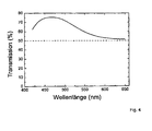
- the transmittance of this embodiment is up to about 70% in the visible range (cf. Fig. 4 ).
- This transparent red pin OLED shows an emission maximum at about 620nm.
- the emission brightness for a measurement by the ITO base electrode is 1200 cd / m 2
- the emission brightness is 380 cd / m 2 . This corresponds to a ratio of 3.1.
- the optical transmittance of the device is in many parts of the visible spectrum between 60% and 70%.
Landscapes
- Physics & Mathematics (AREA)
- Optics & Photonics (AREA)
- Electroluminescent Light Sources (AREA)
Description
Die Erfindung bezieht sich auf ein transparentes lichtemittierendes Bauelement, insbesondere eine organische Leuchtdiode, mit einer transparenten Schichtanordnung, bei der auf einem Substrat in einem Stapel flächige Elektroden und ein zwischen den flächigen Elektroden angeordneter organischer Bereich, welcher eine lichtemittierende Schicht umfasst, aus einem oder mehreren organischen Materialien gebildet sind.The invention relates to a transparent light-emitting component, in particular an organic light-emitting diode, with a transparent layer arrangement, in which planar electrodes are arranged on a substrate in a stack and an organic region arranged between the planar electrodes, which comprises a light-emitting layer, of one or more organic materials are formed.
Organische Leuchtdioden (OLED) gewinnen in den letzten Jahren verstärkt Aufmerksamkeit aufgrund ihres hohen Potentials für Anwendungen im Bereich der Beleuchtung und der Anzeige von Informationen. Hierbei sind eine Vielzahl von Aspekten organischer Leuchtdioden von Bedeutung, unter anderem ihr Potential für hohe Leistungseffizienzen, ihre Verwendbarkeit auf flexiblen Substraten, ihre Steuerbarkeit der Farbemission sowie die Möglichkeit, transparente OLEDs als Beleuchtungselemente oder Anzeigeelemente zu verwenden. Insbesondere als Flächenstrahler sind OLEDs grundsätzlich verschieden, zu bekannten Beleuchtungstechniken, beispielsweise anorganischen Leuchtdioden, Glühlampen oder Leuchtstoffröhren. Sie stellen eine völlig neue Technik dar, welche die Anwendungsvielfalt erweitern kann.Organic Light Emitting Diodes (OLEDs) have received increasing attention in recent years because of their high potential for lighting applications and information display. Here are a variety of aspects of organic light emitting diodes of importance, including their potential for high power efficiencies, their usability on flexible substrates, their controllability of color emission and the ability to use transparent OLEDs as lighting elements or display elements. In particular, as a surface radiator OLEDs are fundamentally different, to known lighting techniques, such as inorganic light emitting diodes, incandescent or fluorescent tubes. They represent a completely new technology that can expand the variety of applications.
Eine Realisation von Fensterscheiben basierend auf transparenten. OLEDs wäre eine solche Anwendung, wobei als Maß für die Transparenz der OLED üblicherweise der Transmissionsgrad für auf die OLED einfallendes Licht herangezogen wird. Derartige Fensterscheiben würden es ermöglichen, architektonisch Beleuchtungselemente vorzusehen, welche zum einen das Tageslicht ausnutzen, andererseits aber auch selbständig leuchten können. Ebenfalls sind transparente Displays interessant, die zum Beispiel in Frontscheiben von Verkehrsmitteln eingebaut werden und den Führer des Verkehrsmittels mit Informationen versorgen können. Ferner besteht der Wunsch, vor Objekte, auf die die Sicht frei, bleiben soll, transparente Beleuchtungs- oder Anzeigeelemente zu setzen. So kann zum Beispiel im Fahrzeug vor dem Geschwindigkeitsmesser ein transparentes Display plaziert werden, das den Fahrer beispielsweise vor einer angezogenen Handbremse warnt, ansonsten aber ausgeschaltet ist.A realization of windows based on transparent. OLEDs would be such an application, whereby the transmittance for light incident on the OLED is usually used as a measure of the transparency of the OLED. Such windows would make it possible to provide architectural lighting elements, which on the one hand take advantage of daylight, on the other hand, but can also shine independently. Also, transparent displays are interesting, which are installed for example in windscreens of transport and can provide the leader of the transport with information. There is also a desire to set transparent lighting or display elements in front of objects to which vision is to remain free. For example, in the vehicle in front of the speedometer, a transparent display can be placed, which warns the driver, for example, of a handbrake applied, but otherwise is switched off.
Bei einer solchen Verwendung transparenter OLEDs geht jedoch ein Anteil von etwa 50% des emittierten Lichtes verloren, da üblicherweise das im lichtemittierenden organischen Bereich der OLED erzeugte Licht durch die beiden OLED-Außenflächen auf der Ober- und der Unterseite näherungsweise zu gleichen Teilen emittiert wird. Hierdurch werden die Effektivität des Beleuchtungselements oder die Helligkeit des Displays drastisch reduziert, wodurch eine mögliche kommerzielle Anwendung erschwert ist.With such a use of transparent OLEDs, however, a proportion of about 50% of the emitted light is lost, since usually the light generated in the light-emitting organic region of the OLED is emitted by the two OLED outer surfaces on the top and the bottom approximately equal parts. As a result, the effectiveness of the lighting element or the brightness of the display are drastically reduced, whereby a possible commercial application is difficult.
Transparente OLEDs sind als solche bereits bekannt, beruhend auf der Verwendung von zwei transparenten Elektroden, die beispielsweise aus leitfähigen Gläsern wie ITO oder dünnen Metallen oder Kombinationen hiervon bestehen können. Im Gegensatz zu transparenten OLEDs verfügen klassische OLEDs über genau eine transparente Elektrode, während die zweite Elektrode aus einem reflektierenden Metall besteht, wodurch das Licht ausschließlich durch die transparente Elektrode emittiert wird.Transparent OLEDs are already known per se, based on the use of two transparent electrodes, which may for example consist of conductive glasses such as ITO or thin metals or combinations thereof. In contrast to transparent OLEDs, classic OLEDs have exactly one transparent electrode, while the second electrode consists of a reflecting metal, whereby the light is emitted exclusively through the transparent electrode.
Es gibt Bernühungen, transparente OLEDs mit sogenannten schaltbaren Spiegeln zu verbinden. Hierbei wird zusammen mit der OLED der Spiegel eingeschaltet und das gesamte Licht der OLED in dieselbe Richtung gesandt. Diese Variante ist jedoch sehr aufwendig und kostenintensiv.There are efforts to connect transparent OLEDs with so-called switchable mirrors. In this case, the mirror is switched on together with the OLED and the entire light of the OLED is sent in the same direction. However, this variant is very complicated and expensive.
Es gibt auch noch einen weiteren Ansatz, nach dem semitransparente organische Leuchtdioden gebaut werden, die eine hochtransparente und eine, bedingt durch hohe Absorptionsverluste, weniger transparente Elektrode haben. Eine größere Lichtmenge wird hierbei durch die hochtransparente Elektrode abgestrahlt. Allerdings wird bei diesem Ansatz die ungleiche Lichtabstrahlung lediglich durch Absorption in der weniger transparenten Elektrode erkauft, das heißt eine Verringerung der Effizienz der OLED findet statt. Darüber hinaus leidet der Gesamttransmissionsgrad der OLED unter der niedrigeren Transparenz der einen Elektrode. Ein vereinfachtes Rechenbeispiel soll das verdeutlichen: Unter der Annahme, dass die organischen Schichten einen Transmissionsgrad von 1 aufweisen, eine Elektrode einen Transmissionsgrad von 0.6 und die zweite einen Transmissionsgrad von 0.9, hat die OLED in erster Näherung einen Transmissionsgrad von knapp über 50%. Von allen Photonen, die das Bauelement verlassen, werden zwei Fünftel durch die eine Elektrode und drei Fünftel durch die andere Elektrode emittiert. 25% der Photonen, die auch das Bauelement verlassen hätten, werden in den Elektroden absorbiert. Soll nun statt einem Verhältnis der abgestrahlten Lichtintensitäten auf den beiden Seiten des Bauelementes von 2:3 ein Verhältnis von 1:4 realisiert werden, müssten schon Elektroden mit einem Transmissionsvermögen von 0.9 und 0.22 genutzt werden. Der Transmissionsgrad des Bauelementes betrüge dann nur noch 20% und 44% der Photonen, die eigentlich das Bauelement verlassen würden, werden in den Elektroden absorbiert. Der Transmissionsgrad von 90% für die höher transparente Elektrode wurde in dieser Rechnung verwendet, da dies bereits einen sehr hohen Wert für transparente und leitfähige Elektroden darstellt. Unter besonders idealen Bedingungen sind auch 95% erreichbar, was aber an der Rechnung nichts grundlegend ändert.There is also another approach, according to which semitransparent organic light emitting diodes are built, which have a highly transparent and, due to high absorption losses, less transparent electrode. A larger amount of light is emitted through the highly transparent electrode. However, in this approach, the uneven light emission is only paid for by absorption in the less transparent electrode, that is, a reduction in the efficiency of the OLED takes place. In addition, the overall transmittance of the OLED suffers from the lower transparency of one electrode. A simplified calculation example is intended to clarify this: Assuming that the organic layers have a transmittance of 1, one electrode has a transmittance of 0.6 and the second a transmittance of 0.9, the OLED has, to a first approximation, a transmittance of just over 50%. Of all the photons leaving the device, two-fifths are emitted through one electrode and three-fifths through the other electrode. 25% of the photons that have also left the device are absorbed in the electrodes. If, instead of a ratio of the radiated light intensities on the two sides of the component of 2: 3, a ratio of 1: 4 is realized, electrodes with a transmissivity of 0.9 and 0.22 would already have to be used become. The transmittance of the device would then be only 20% and 44% of the photons that would actually leave the device are absorbed in the electrodes. The transmittance of 90% for the higher transparent electrode was used in this calculation, since this already represents a very high value for transparent and conductive electrodes. 95% are achievable under particularly ideal conditions, but this does not change anything fundamentally on the bill.
In dem Dokument
Das Dokument
Im Dokument
In dem Dokument
Weiterhin ist aus dem Dokument
Aufgabe der Erfindung ist es, ein transparentes lichtemittierendes Bauelement, insbesondere eine organische Leuchtdiode, zu schaffen, mit dem die Anwendungsmöglichkeiten für transparente lichtemittierende Bauelemente erweitert werden.The object of the invention is to provide a transparent light-emitting component, in particular an organic light-emitting diode, with which the application possibilities for transparent light-emitting components are extended.
Diese Aufgabe wird erfindungsgemäß durch ein transparentes lichtemittierendes Bauelement nach dem unabhängigen Anspruch 1 gelöst. Vorteilhafte Ausgestaltungen der Erfindung sind Gegenstand von abhängigen Unteransprüchen.This object is achieved by a transparent light emitting device according to independent claim 1. Advantageous embodiments of the invention are the subject of dependent subclaims.
In dem organischen Bereich sind eine oder mehrere dotierte Ladungsträger-Transportschichten gebildet.One or more doped carrier transport layers are formed in the organic region.
Mit der Erfindung ist ein transparentes lichtemittierendes Bauelement, insbesondere eine organische Leuchtdiode (OLED), zur Verfügung gestellt, welches eine bevorzugte Emission des Lichtes durch eine der beiden Elektroden mit einer hohen Gesamttransparenz des Bauelementes in zumindest einer Einfallsnchtung vereint. Ein solches Bauelement kann insbesondere als ein Beleuchtungselement Verwendung finden, welches Gebäudeinnenräume zur Außenwelt abgrenzt, beispielsweise in Form einer Fensterscheibe. Diese Bauelemente können dann während Tageslichteinfall das, Gebäudeinnere mit Licht versorgen, ohne dass sich das lichtemittierende Bauelement in einem Betriebszustand befindet. Bei Abnahme des Tageslichtes kann das Bauelement dann angeschaltet werden, wobei das erzeugte Licht bevorzugt in das Gebäudeinnere emittiert wird, wodurch die Ausnutzung der Leuchtleistung erheblich verbessert wird. Darüber hinaus ist die Verwendung eines entsprechenden Bauelementes auch in anderen Anwendungsbereichen möglich, beispielsweise einzeln oder als Kombination von mehreren lichtemittierenden Bauelementen in einem aktiven oder einem, passiven Anzeigenelement oder einem Display oder auch in einer Beleuchtungsvorrichtung, beispielsweise in Fahrzeugen oder als Raumbelenchtung.The invention provides a transparent light-emitting component, in particular an organic light-emitting diode (OLED), which provides a preferred emission of the light through one of the two electrodes with a high overall transparency of the component united in at least one incident. Such a component can be used in particular as a lighting element which delimits building interiors to the outside world, for example in the form of a window pane. These components can then provide the interior of the building with light during daylight incidence, without the light-emitting component being in an operating state. When the daylight is removed, the component can then be switched on, wherein the generated light is preferably emitted into the building interior, whereby the utilization of the luminous power is considerably improved. In addition, the use of a corresponding component in other applications is possible, for example, individually or as a combination of multiple light emitting devices in an active or a passive display element or a display or in a lighting device, such as in vehicles or Raumbelenchtung.
Gegenüber dem Stand der Technik hat die Erfindung weiterhin den Vorteil, dass nicht ein Großteil des im lichtemittierenden organischen Bereich erzeugten Lichtes aufgrund von Absorption verlorengeht.Compared to the prior art, the invention has the further advantage that not a large part of the light generated in the light-emitting organic region is lost due to absorption.
In bevorzugten Ausführungsformen kann bei der Elektrode die Oxidschicht aus dem elektrisch leitfähigen Oxidmaterial eine Dicke von wenigstens 15nm, bevorzugt von wenigstens 25nm, vorzugsweise von wenigstens 40nm oder weiter bevorzugt von wenigstens 60nm aufweisen. Höhere Schichtdicken lassen sich zuverlässiger herstellen und erleichtern die Stromzuführung.In preferred embodiments, in the electrode, the oxide layer of the electrically conductive oxide material may have a thickness of at least 15 nm, preferably at least 25 nm, preferably at least 40 nm or more preferably at least 60 nm. Higher layer thicknesses can be produced more reliably and facilitate the power supply.
Zweckmäßige Ausgestaltungen der Erfindung sehen vor, dass bei der anderen Elektrode die Metallschicht eine Dicke von weniger als 30nm, bevorzugt von weniger als 20nm oder vorzugsweise von weniger als 10nm aufweisen. Mit abnehmender Schichtdicke nimmt der Transmissionsgrad zu.Advantageous embodiments of the invention provide that in the case of the other electrode the metal layer has a thickness of less than 30 nm, preferably less than 20 nm or preferably less than 10 nm. As the layer thickness decreases, the transmittance increases.
Die Erfindung wird im folgenden anhand von Ausführungsbeispielen unter Bezugnahme auf die Figuren einer Zeichnung näher erläutert. Hierbei zeigen:
- Fig. 1
- eine schematische Darstellung eines transparenten lichtemittierenden Bauelementes mit einer transparenten Schichtanordnung;
- Fig. 2
- eine graphische Darstellung der Leuchtdichte in Abhängigkeit von der Spannung für ein transparentes lichtemittierendes Bauelement nach einem Ausführungsbeispiel;
- Fig. 3
- eine graphische Darstellung der Stromeffizienz in Abhängigkeit von der Spannung für das transparente lichtemittierende Bauelement nach dem Ausführungsbeispiel; und
- Fig. 4
- eine graphische Darstellung des Transmissionsgrades in Abhängigkeit von der Wellenlänge für das transparente lichtemittierende Bauelement nach dem Ausftihrungsbeispiel.
- Fig. 1
- a schematic representation of a transparent light-emitting device with a transparent layer arrangement;
- Fig. 2
- a graph of the luminance as a function of the voltage for a transparent light emitting device according to an embodiment;
- Fig. 3
- a graph of the current efficiency as a function of the voltage for the transparent light-emitting device according to the embodiment; and
- Fig. 4
- a graphical representation of the transmittance as a function of the wavelength for the transparent light-emitting device according to the Ausftihrungsbeispiel.
Mittels der Dotierung der Ladungsträger-Transportschichten 9, 10 ist zum einen der Ladungsträgertransport nicht von der Schichtdicke abhängig, was eine freie Wahl der verwendeten Schichtdicken erlaubt und eine Optimierung des Schichtaufbaus auf das gewünschte Auskopplungsverhalten ermöglicht. Andererseits wird mit der Dotierung der Ladungsträger-Transportschichten 9, 10 die Begrenzung der verwendbaren Materialien für die Elektroden 5, 6 aufgehoben, wie sie bei OLEDs mit undotierten Transportschichten besteht. Eine Anpassung der Austrittsarbeit der Elektrode an die Energieniveaus der angrenzenden organischen Schicht ist aufgrund der Dotierung nicht notwendig, so dass eine freie Wahl des Elektrodenmaterials auf beiden Seiten der OLED möglich ist.By means of the doping of the charge
Das in
Eine der flächigen Elektroden 5, 6 umfasst eine Metallschicht mit einer Dicke von weniger als 40nm und die andere der flächigen Elektroden 5, 6, welche in der transparenten Schichtanordnung 1 der Elektrode gegenüberliegend angeordnet ist, weist eine Oxidschicht aus einem elektrisch leitfähigen Oxidmaterial mit einer Dicke von wenigstens 10nm auf. Für eine auf einer Seite der transparenten Schichtanordnung 1 austretende Lichtemission und eine auf einer gegenüberliegenden Seite der transparenten Schichtanordnung 1 austretende Lichtemission ist ein Intensitätsverhältnis von mindestens 2:1 gebildet. Ein Transmissionsgrad der transparenten Schichtanordnung 1 für wenigstens einen Wellenlängenteilbereich im sichtbaren Spektralbereich ist für zumindest eine Einfallsrichtung größer als 50%.One of the sheet-
zur Realisierung einer organischen Leuchtdiode, wie sie in
Die im folgenden vorgestellten Ausführungsbeispiele zur weiteren Erläuterung der Erfindung wurden zunächst mit Hilfe einer Computersimulation berechnet, dann wurde an ausgewählten Beispielen die Übereinstimmung der theoretisch bestimmten Ergebnisse mit tatsächlich hergestellten und vermessenen OLEDs überprüft und bestätigt.The exemplary embodiments presented below for further explanation of the invention were first calculated using a computer simulation, then the conformity of the theoretically determined results with actually produced and measured OLEDs was checked and confirmed on selected examples.
Es kann vorgesehen sein, die Auskoppelung des Lichtes durch die gewünschte der Elektroden 5, 6 mittels geeigneter Maßnahmen weiter zu optimieren, beispielsweise mittels Verwendung einer Auskoppelfolie, einer Entspiegelungsschicht, oder dergleichen., wodurch zum Einen das Verhältnis der Emissionen durch Vorder- und Rückseite weiter vergrößert wird, zum anderen gegebenenfalls auch die Gesamttransparenz des Bauelementes verbessert wird.It can be provided to further optimize the decoupling of the light by the desired one of the
Die Effizienz des Bauelementes lässt sich ferner verbessern, indem zwischen dem transparenten Substrat und der dem transparenten Substrat zugewandten flächigen Elektrode eine weitere Schicht (nicht dargestellt) mit einem Brechungsindex kleiner als 1.4 eingebracht wird. Mittels dieser Schicht wird die Auskopplung des emittierten Lichtes aus dem organischen Bereich in das Substrat unterstützt und gegebenenfalls auch das Abstrahlverhältnis erhöht.The efficiency of the component can be further improved by introducing a further layer (not shown) with a refractive index of less than 1.4 between the transparent substrate and the planar electrode facing the transparent substrate. By means of this layer, the coupling out of the emitted light from the organic region into the substrate is supported and optionally also the emission ratio is increased.
Bei einem Ausführungsbeispiel sind eine ITO-Schicht auf einem. Glassubstrat mit einer Dicke von 60nm als transparente und eine dünne Metallschicht als semitransparente Gegenelektrode vorgesehen. Damit die Metallschicht semitransparent ist, muss diese ausreichend dünn gewählt werden. Dies ist jedoch nicht bei jedem Metall möglich ohne dass die Leitfähigkeit der Schicht zu stark verringert wird. Beispielsweise muss bei Aluminiumschichten die Schichtdicke des Metalls kleiner als 4nm sein, damit eine Gesamttrausparenz der Schichtanordnung von 50% erreicht wird. Eine solch dünne Schicht würde jedoch nicht ausreichen um das Bauelement über diese Elektrode mit dem nötigen Strom zu versorgen.In one embodiment, an ITO layer is on top of one. Glass substrate with a thickness of 60nm as a transparent and a thin metal layer as a semitransparent counter electrode provided. For the metal layer to be semitransparent, it must be sufficiently thin. However, this is not possible with any metal without unduly reducing the conductivity of the layer. For example, in the case of aluminum layers, the layer thickness of the metal must be less than 4 nm in order to achieve a total transparency of the layer arrangement of 50%. However, such a thin layer would not be sufficient to supply the device via this electrode with the necessary power.
Um den Gesamttransmissionsgrad des Bauelementes trotz dickerer Aluminiumschicht auf 50% zu halten, kann eine zusätzliche Schicht mit einem Brechungsindex größer als 1.3 auf der von der OLED abgewandten Seite aufgebracht werden. Diese zusätzliche Schicht dient als eine Art Auskoppelschicht oder Entspiegelungsschicht und reduziert gleichzeitig die Absorption der Lichtrnode in der Metallschicht. Bei der zusätzlichen Schicht kann es sich um eine im sichtbaren Spektralbereich transparente organische Schicht handeln, wie zum Beispiel Meo-TPD (NN,NNI-Tetrakis(4-methoxyphenyl)-benzidin,e) oder Spiro-TAD (2,2',7,7'-Tetrakis-(N,N-diphenylamino)-9,9'-spirobifluoren), welche im sichtbaren Spektralbereich einen Brechungsindex von etwa 1.7 aufweisen. Mit Hilfe einer 80nm dicken Meo-TPD-Schich.t kann eine Al-Dicke von 8nm verwendet werden.. um einen Gesaznttransmissivnsgrad von 50% zu erzielen. Dieser Effekt wird umso stärker je höher der Brechungsindex des verwendeten Materials ist.In order to keep the total transmission of the device despite thicker aluminum layer to 50%, an additional layer with a refractive index greater than 1.3 on the side facing away from the OLED side can be applied. This additional layer serves as a kind of decoupling layer or antireflection layer and at the same time reduces the absorption of the light strands in the metal layer. The additional layer may be an organic layer which is transparent in the visible spectral region, for example Meo-TPD (NN, NNI-tetrakis (4-methoxyphenyl) -benzidine, e) or spiro-TAD (2,2 ', 7 , 7'-tetrakis (N, N-diphenylamino) -9,9'-spirobifluorene), which have a refractive index of about 1.7 in the visible spectral range. Using an 80nm thick Meo-TPD layer, an Al thickness of 8nm can be used to achieve a total transmissivity of 50%. This effect becomes stronger the higher the refractive index of the material used.
Eine besonders vorteilhafte Ausführung der zusätzlichen Schicht ist gebildet, wenn diese nicht nur im sichtbaren Spektralbereich transparent, sondern auch noch elektrisch leitfähig ist, wie das bei vielen Metalloxiden, zum Beispiel ITO, IZO, ZnO, TiO2, der Fall, ist. Dies hat den Vorteil, dass sich die elektrische Leitfähigkeit jetzt aus der Metallschicht und der zusätzlichen Schicht ergibt. Für den bereits erwähnten Fall der 5nm dicken Al-Schicht in Kombination mit einer 40nm dicken ITO-Schicht hieße dies, dass diese Schicht eine ausreichend hohe Leitfähigkeit aufweist. Unter einer ausreichend hohen Leitfähigkeit wird ein Flächenwiderstand der Elektrode von weniger als 200 Ohm/square, bevorzugt weniger als 30 Ohm/square verstanden. Die Gesamttransmission der OLED liegt aufgrund des hohen Brechungsindexes von ITO, welcher im sichtbaren Spektralbereich 1.8 bis 2 beträgt, sogar bei 70%. Weiterhin besteht hierbei die Möglichkeit, mittels Variation der Schichtdicken von ITO und A1 sowohl den Gesamttransmissionsgrad, das Abstrahlverhältnis und die Effizienz; des Bauelementes zu variieren. Bei einer transparenten roten OLED mit einem Emissionspeak bei 630nm führt beispielsweise eine Erhöhung der Al-Dicke von 5nm auf 8nm zu einem Rückgang der Gesamttransmission von 70% auf 55%. Das Abstrahlverhältnis, gemessen anhand der Intensität des abgestrahlten Lichtes auf der Oberseite und der Substratseite des Bauelementes, ändert sich jedoch von 1:5 auf 1:10 bei einer gleichzeitigen Effizienzsteigerung des Bauelementes um 40% auf der Substratseite.A particularly advantageous embodiment of the additional layer is formed when it is not only transparent in the visible spectral range but also electrically conductive, as is the case with many metal oxides, for example ITO, IZO, ZnO,
Mittels Aufbringen einer Auskopplungsschicht auf der von dem organischen Bereich abgewandten Substratseite kann die Effizienz und damit auch das Abstrahlverhältnis, je nach WirKungsgrad der Auskopplungsschicht, noch mal deutlich verbessert werden. Beispielsweise können mit einer einfachen Streufolie Verbesserungen von 40% erzielt werden.By applying a coupling-out layer on the side of the substrate facing away from the organic region, the efficiency and thus also the emission ratio, depending on the degree of efficiency of the coupling-out layer, can again be significantly improved. For example, with a simple scattering film, improvements of 40% can be achieved.
Als besonders vorteilhaft erweist sich eine Dotierung der Ladungsträger-Transportschichten 9, 10 (vgl.
Auch hier kann, wie oben beschrieben, mittels Aufbringen einer zusätzlichen Schicht auf die Ag-Elektrode die Gesamttransmission der OLED verbessert werden. Mit Hilfe einer 40nm dicken Meo-TPD-Schicht kann diese von 50% auf 70% bis 80% erhöht werden. Jedoch wird beispielsweise bei einer roten OLED auch das Abstrahlverhältnis von 1:10 auf 1:6 verändert.Again, as described above, the total transmission of the OLED can be improved by applying an additional layer to the Ag electrode. With the aid of a 40nm thick Meo-TPD layer, this can be increased from 50% to 70% to 80%. However, for example, with a red OLED, the emission ratio also changes from 1:10 to 1: 6.
Auch hierbei lassen sich mit Hilfe einer geringen Veränderung der Ag-Schichtdicke der Gesamttransmissionsgrad, das Abstrahlverhältnis und die EfFtzienz der OLED variieren. Beispielsweise wird bei einer Änderung der Ag-Dicke von 15nm auf 25nm und einer Abstimmung der Schichten im organischen Bereich des Bauelementes auf die Elektrodenkonfiguration mit einer 40nm dicken zusätzlichen Schicht der Gesamttransmissionsgrad des Bauelementes von 70% bis 80% auf 50% reduziert. Das Abstrahlverhältnis hingegen wird von 1:6 auf 1:14 bei einer Effizienzsteigerung von 40% auf der Substratseite verbessert.In this case too, the total transmission level, the emission ratio and the efficiency of the OLED can be varied with the aid of a small change in the Ag layer thickness. For example, changing the Ag thickness from 15nm to 25nm and matching the layers in the organic region of the device to the electrode configuration with a 40nm thick additional layer reduces the overall transmission of the device from 70% to 80% to 50%. By contrast, the emission ratio is improved from 1: 6 to 1:14 with an increase in efficiency of 40% on the substrate side.
Wie bei der Al-Elelctrode kann auch hierbei mit anderen zusätzlichen Schichten, die einen höheren Brechungsindex als Meo-TPD aufweisen, gearbeitet werden, und die Effizienz und das Abstrahlverhältnis der OLED können gezielt modifiziert werden.As with the Al-Elelctrode, it is also possible here to work with other additional layers which have a higher refractive index than Meo-TPD, and the efficiency and the emission ratio of the OLED can be modified in a targeted manner.
Neben der Kombination von Metallschicht und ITO-Zusatzschicht ist eine weitere Variante, den Kontakt durch eine ITO/Metall/ITO (IMI) Schichtfolge zu ersetzen. Mittels Wahl der Schichtdicken können so extrem transparente Elektroden hergestellt werden, die trotzdem ein ausreichend gutes Reflexionsvermögen besitzen, um zu einer gerichteten Abstrahlung zu führen. Zum Beispiel wurde mit einer 60nm ITO-Grundelektrode auf dem Glassubstrat und einer IMI-Elektmde aus 5nm ITO/ 5nm Ag/ 135nm ITO ein Gesamttransmissionsgrad der OLED von 80% bis 90% im sichtbaren Spektralbereich erreicht. Das Abstrahlverhältnis einer roten OLED beträgt hierbei 1:5 (Oberseite : Substratseite). Wird die Dicke der Ag-Schicht auf 10nm erhöht, sinkt der Gesamttransmissionsgrad der OLED auf 60% bis 80%, das Abstrahlungsverhältnis steigt aber auf 1:9 an, und die Effizienz der OLED in die bevorzugte Abstrahlrichtung erhöht sich um 26%.In addition to the combination of metal layer and ITO additional layer, another alternative is to replace the contact with an ITO / metal / ITO (IMI) layer sequence. By choosing the layer thicknesses, it is possible to produce extremely transparent electrodes which nevertheless have a sufficiently good reflectivity in order to lead to directional radiation. For example, with a 60nm ITO base electrode on the glass substrate and an IMI electrode of 5nm ITO / 5nm Ag / 135nm ITO, a total OLED transmittance of 80% to 90% in the visible spectral range was achieved. The emission ratio of a red OLED is in this case 1: 5 (upper side: substrate side). When the thickness of the Ag layer is increased to 10nm, the total transmittance of the OLED decreases to 60% to 80%, but the irradiation ratio increases to 1: 9, and the efficiency of the OLED in the preferred irradiation direction increases by 26%.
Nach dem Prinzip des semitransparenten Metallkontaktes mit Zusatzschicht wurde bei einer roten OLED mit einem 15nm dicken Au-Kontakt und einer 50nm dicken Meo-TPD-Zusatzschicht bei einem Abstrahlverhältnis von 3:1 ein Gesamtransmissionsgrad des Bauelementes von 90% im roten Spektralbereich erreicht. Da das Transmissionsband wesentlich schmaler ist als der gesamte sichtbare Spektralbereich, kann mittels geeigneter Wahl der Kontaktschicht- und der Zusatzschichtdicke die maximale Transmission an eine bestimmte Stelle des sichtbaren Spektrums verschoben werden, und das transparente lichtemittierende Bauelement dient somit als eine Art Farbfilter. Beispielsweise kann das Maximum der Transmission in den grünen Spektralbereich verschoben werden, wo die Empfindlichkeit des menschlichen Auges am höchsten ist. Die OLED ist jedoch rot oder blau und hat damit eine bessere Reflexion an der Elektrode und folglich eine stärker gerichtete Abstrahlcharakteristik.Following the principle of semitransparent metal contact with additional layer, a total redox emission of 90% in the red spectral region was achieved for a red OLED with a 15nm thick Au contact and a 50nm Meo-TPD additional layer at an emission ratio of 3: 1. Since the transmission band is substantially narrower than the entire visible spectral range, by means of a suitable choice of the contact layer and the additional layer thickness, the maximum transmission can be shifted to a specific point in the visible spectrum, and the transparent light-emitting component thus serves as a kind of color filter. For example, the maximum of the transmission can be shifted to the green spectral range, where the sensitivity of the human eye is highest. However, the OLED is red or blue and thus has better reflection at the electrode and consequently a more directional radiation characteristic.
Bei einer 60nm dicken ITO-Elektrode auf dem Glassubstrat und einer 15nm Au-Gegenelektrode mit einer 160nm dicken Meo-TPD-Zusatzschicht erreicht eine blaue, hinsichtlich der Schichtdicken optimierte OLED mit einem Emissionspeak bei 450nm einen Gesamttransnüssionsgrad von 60% im Spektralbereich zwischen 420 und 600nm. Diese OLED hat ein Abstrahhmgsverhältnis von 1:5 (Oberseite : Substratseite). Mittels bloßer Reduzierung der Zusatzschicht steigt der Transmissionsgrad im grünen Spektralbereich auf 80% an und sinkt im blauen Spektralbereich auf unter 60% ab. Das Abstrahlungsverhältnis steigt auf 1:6, und die Effizienz der OLED in die bevorzugte Abstrahlungsrichtung steigt um 27%.With a 60 nm thick ITO electrode on the glass substrate and a 15 nm Au counterelectrode with a 160 nm thick Meo-TPD additional layer, a blue layer thickness optimized OLED with an emission peak at 450 nm achieves a total transmittance of 60% in the spectral range between 420 and 600 nm , This OLED has an abstraction ratio of 1: 5 (upper side: substrate side). By merely reducing the additional layer, the transmittance in the green spectral range increases to 80% and decreases to below 60% in the blue spectral range. The radiation ratio increases to 1: 6, and the efficiency of the OLED in the preferred direction of radiation increases by 27%.
Dieser Effekt wird noch verstärkt, wenn die Meo-TPD-Schicht durch eine Schicht mit höherem Brechungsindex ersetzt wird, zum Beispiel eine Schicht aus TiO2 oder ZnS. Bei einer 180nm dicken TiO2-Schicht steigt der Transmissionsgrad im grünen Spektralbereich auf 80% an und sinkt im blauen und roten Spektralbereich auf unter 50% ab. Auch hier beträgt das Abstrahlungsverhältnis 1:6.This effect is exacerbated when the Meo-TPD layer is replaced by a layer of higher refractive index, for example a layer of
Wie bereits erläutert wird mittels Dotierung der Ladungsträger-Transportschichten eine weitreichende Freiheit bei der Wahl des Materials für die Elektroden erreicht. Dies bedeutet, dass es auch möglich ist, die beiden Elektroden miteinander zu vertauschen. Zum Beispiel kann eine 15nm dicke Ag-Schicht auf das Glassubstrat aufgebracht werden, und nach dem Auf bringen der organischen Schichten wird eine 80nm dicke ITO-Schicht als Elektrode auf die OLED aufgesputtert. Der Vorteil dieser Bauform besteht darin, dass das Glassubstrat aufgrund seines Brechungsindexes von 1.45 im sichtbaren Spektralbereich bereits die oben beschriebene Funktion der Zusatzschicht übernimmt. Der Gesamttransmissionsgrad der OLED liegt dadurch bereits bei 75%, das Abstrahlverhältnis in beide Richtungen ist jedoch nahezu identisch. Mittels Erhöhung der Ag-Dicke auf 21nm wird zwar die Gesamttransmission auf 55% reduziert, das Abstrahlverhältnis jedoch auf 2:1 verbessert.As already explained, by means of doping of the charge carrier transport layers, a far-reaching freedom in the choice of the material for the electrodes is achieved. This means that it is also possible to swap the two electrodes together. For example, a 15 nm thick Ag layer can be applied to the glass substrate, and after the organic layers are applied, an 80 nm thick ITO layer is sputtered onto the OLED as an electrode. The advantage of this design is that due to its refractive index of 1.45 in the visible spectral range, the glass substrate already performs the function of the additional layer described above. Thus, the total transmission of the OLED is already at 75%, but the radiation ratio in both directions is almost identical. By increasing the Ag thickness to 21nm, the total transmission is reduced to 55%, but the emission ratio is improved to 2: 1.
Die Verwendung einer ITO / Metall / ITO-Elektrode ist nicht in jedem Fall von Vorteil. Eine Deckelektrode mit 5nm ITO / 10nm Ag / 65nm ITO und eine 15nm dicke Ag-Elektrode auf der Substratseite würde zwar die Leitfähigkeit der Elektrode verbessern und trotzdem einen Gesamttransmissionsgrad von 70% erreichen, das Abstrahlverhältnis in beide Richtungen wäre jedoch wieder annähernd gleich. Um das Abstrahlverhältnis bei einer Gesamttransmission von über 50% auf 2:1 zu bringen, müsste die Ag-Dicke auf der Substratseite 20nm betragen.The use of an ITO / metal / ITO electrode is not always an advantage. Although a cover electrode with 5nm ITO / 10nm Ag / 65nm ITO and a 15nm thick Ag electrode on the substrate side would improve the conductivity of the electrode and still achieve a total transmission of 70%, the radiation ratio in both directions would be almost equal again. In order to bring the emission ratio to 2: 1 with a total transmission of more than 50%, the Ag thickness on the substrate side would have to be 20 nm.
Im folgenden werden unter Bezugnahme auf die
Ein organisches lichtemittierendes Bauelement wurde wie folgt hergestellt. Ein mit ITO beschichtetes Glassubstrat wurde zum Ausbilden der Grundelektrode strukturiert und gereinigt. Die Dicke der ITO-Schicht beträgt etwa 130nm bei einem Flächenwiderstand von etwa 20 Ω/∀. Folgende Schichten wurden nacheinander mittels thermischen Verdampfens im Vakuum bei einem Druck von etwa 10-7mbar aufgebracht, wobei das Vakuum nicht gebrochen wurde:
- 1) 65nm N,N,N,N'-Tetrakis(4-methoxyphenyl)-benzidine (MeO-TPD)
dotiert mit - 2)
10nm - 3)
6nm dotiert mit 8% fac-Tris(2-phenylpyridine) Iridium (Ir(ppy)3) bezogen auf die Masse; - 4) 12nm 3-Phenyl-4-(18-naphthyl)-5-phenyl-1,2,4-triazole (TAZ)
dotiert mit 8% fac-Tris(2-phenylpyridine) Iridium (Ir(ppy)3) bezogen auf die Masse; - 5) 10nm Bathophenanthroline (Bphen) als Zwischenschicht;
- 6) 50nm Bphen dotiert mit Cs im molekularen Verhältnis von 1:1 als n-dotierte Elektronen-Transportschicht;
- 7) 15nm Silber als Kathode; und
- 8) 45nm MeO-TPD als Deckschicht.
- 1) 65nm N, N, N, N'-tetrakis (4-methoxyphenyl) benzidines (MeO-TPD) doped with 2,3,5,6-tetrafluoro-7,7,8,8-tetracyanoquinodimethane (F4-TCNQ ) in the molecular ratio of 50: 1 as p-doped hole transport layer;
- 2)
10nm - 3)
6nm - 4) 12nm of 3-phenyl-4- (18-naphthyl) -5-phenyl-1,2,4-triazole (TAZ) doped with 8% fac-tris (2-phenylpyridine) iridium (Ir (ppy) 3 ) to the crowd;
- 5) 10nm bathophenanthroline (Bphen) as intermediate layer;
- 6) 50nm Bphen doped with Cs in the molecular ratio of 1: 1 as n-doped electron transport layer;
- 7) 15nm silver as a cathode; and
- 8) 45nm MeO-TPD as a topcoat.
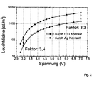
Diese transparente grüne pin-OLED zeigt ein Emissionsmaximum bei etwa 520nm. Bei einer angelegten Spannung von 7V beträgt die Emissionshelligkeit bei Messung durch die ITO-Grundelektrode 4800cd/m2, bei Messung durch den Ag-Deckelektrode hingegen 1400cd/ m2. Das entspricht einem Emissionsverhältnis von 3,4 (vgl.
Ein weiteres organisches Bauelement wurde wie folgt hergestellt. Ein mit ITO beschichtetes Glassubstrat wurde strukturiert und gereinigt. Die Dicke des ITO beträgt etwa 130nm bei einem Flächenwiderstand von etwa 20Ω/∀. Folgende Schichten wurden nacheinander mittels thermischen Verdampfens im Vakuum bei einem Druck von etwa 10-7mbar aufgebracht, wobei das Vakuum nicht gebrochen wurde:
- 1) 40nm N,N,N,N'-Tetrakis(4-methoxyphenyl)-benzidine (MeO-TPD)
dotiert mit - 2) 10nm N,N'-Di(naphtalen-1-yl)-N,N'-diphenyl-benzidin (α-NPD) als Zwischenschicht;
- 3)
20nm dotiert mit 20 % Iridium (III) Tris(1-phenylisoquinoline) bezogen auf die Masse; - 4) 10nm Bathophenanthroline (Bphen) als Zwischenschicht;
- 5) 40nm Bphen dotiert mit Cs im molekularen Verhältnis von 1:1 als n-dotierte Elektronentransportschicht; und
- 6) 15nm Silber als Kathode;
- 1) 40nm N, N, N, N'-tetrakis (4-methoxyphenyl) benzidines (MeO-TPD) doped with 2,3,5,6-tetrafluoro-7,7,8,8-tetracyanoquinodimethane (F4-TCNQ ) in the molecular ratio of 50: 1 as p-doped hole transport layer;
- 2) 10nm N, N'-di (naphthalen-1-yl) -N, N'-diphenylbenzidine (α-NPD) as an intermediate layer;
- 3)
20nm - 4) 10nm bathophenanthroline (Bphen) as intermediate layer;
- 5) 40nm Bphen doped with Cs in the molecular ratio of 1: 1 as n-doped electron transport layer; and
- 6) 15nm silver as cathode;
Diese transparente rote pin-OLED zeigt ein Emissionsmaximum bei etwa 620nm. Bei einer angelegten Spannung von 3.4V beträgt die Emissionshelligkeit bei einer Messung durch die ITO-Grundelektrode 1200cd/m2, bei der Messung durch die Ag-Deckelektrode hingegen 380cd/m2. Das entspricht einem Verhältnis von 3.1. Der optische Transmissionsgrad des Bauelementes beträgt in weiten Teilen des sichtbaren Spektrums zwischen 60% und 70 %.This transparent red pin OLED shows an emission maximum at about 620nm. At an applied voltage of 3.4V, the emission brightness for a measurement by the ITO base electrode is 1200 cd / m 2 , whereas for the measurement by the Ag cover electrode, the emission brightness is 380 cd / m 2 . This corresponds to a ratio of 3.1. The optical transmittance of the device is in many parts of the visible spectrum between 60% and 70%.
Mit Hilfe der Erfindung ist es ermöglicht, eine transparente organische Leuchtdiode herzustellen, deren unterschiedliche Abstrahlung auf den beiden Außenseiten nicht auf der Tatsache beruht, dass ein großer Anteil des im lichtemittierenden Bereich erzeugten Lichtes auf seinem Weg durch eine der beiden Elektroden absorbiert wird, was zu einer Verringerung der Effizienz der OLED führen würde. Es wird vielmehr ein Unterschied in der Abstrahlintensität mittels eines erhöhten Reflexionsvermögens der einen Elektrode bei einer gleichzeitig hohen Gesamttransparenz der OLED realisiert.With the aid of the invention, it is possible to produce a transparent organic light emitting diode, whose different radiation on the two outer sides is not due to the fact that a large proportion of the light generated in the light emitting area is absorbed on its way through one of the two electrodes, resulting in a reduction in the efficiency of the OLED. Rather, a difference in the emission intensity is realized by means of an increased reflectivity of the one electrode with simultaneously high overall transparency of the OLED.
Die in der vorstehenden Beschreibung, den Ansprüchen und der Zeichnung offenbarten Merkmale der Erfindung können sowohl einzeln als auch in beliebiger Kombination für die Verwirklichung der Erfindung in ihren verschiedenen Ausführungsformen von Bedeutung sein.The features of the invention disclosed in the foregoing description, in the claims and in the drawing may be of importance both individually and in any combination for the realization of the invention in its various embodiments.
Claims (19)
- Transparent light-emitting component having a transparent layer arrangement in which are formed, on a transparent substrate in a stack, planar electrodes and an organic region arranged between the planar electrodes, which organic region comprises a light-emitting layer, made from one or a plurality of organic materials, wherein:- for at least one direction of incidence, a transmittance of the transparent layer arrangement for at least one wavelength subrange in the visible spectral range is greater than 50%,- one of the planar electrodes has an oxide layer made from an electrically conductive oxide material having a thickness of at least 10 nm,- one or a plurality of doped charge carrier transport layers are formed in the organic region,characterized in that another of the planar electrodes, which is arranged opposite to the electrode in the layer arrangement, has a metal layer having a thickness of less than 40 nm, an intensity ratio of at least 2:1 is formed for a light emission emerging on one side of the transparent layer arrangement and a light emission emerging on an opposite side of the transparent layer arrangement, and a coupling-out layer made from an organic material for coupling out light is formed on the electrode and/or the other electrode.
- Transparent light-emitting component according to Claim 1, characterized in that the electrode and/or the other electrode is a multilayer electrode.
- Transparent light-emitting component according to Claim 2, characterized in that the multilayer electrode comprises at least one oxide layer made from an electrically conductive oxide material and at least one metal layer.
- Transparent light-emitting component according to Claim 2, characterized in that the multilayer electrode comprises a plurality of oxide layers made from in each case an electrically conductive oxide material and/or a plurality of metal layers.
- Transparent light-emitting component according to Claim 3 or 4, characterized in that one or all of the oxide layers of the multilayer electrode have a thickness of at least 10 nm.
- Transparent light-emitting component according to one of Claims 3 to 5, characterized in that one or all of the metal layers of the multilayer electrode have a thickness of less than 40 nm.
- Transparent light-emitting component according to one of the preceding claims, characterized in that the coupling-out layer is electrically conductive.
- Transparent light-emitting component according to one of the preceding claims, characterized in that the coupling-out layer has a refractive index of at least 1.3.
- Transparent light-emitting component according to one of the preceding claims, characterized in that the coupling-out layer has a refractive index of at least 1.6.
- Transparent light-emitting component according to one of the preceding claims, characterized in that a coupling-out layer is applied on a side of the transparent substrate which is remote from the organic region.
- Transparent light-emitting component according to Claim 10, characterized in that the coupling-out layer is formed by means of a coupling-out film.
- Transparent light-emitting component according to one of the preceding claims, characterized in that, for the at least one direction of incidence, the transmittance of the transparent layer arrangement for at least one wavelength subrange in the visible spectral range is greater than 60%.
- Transparent light-emitting component according to one of Claims 1 to 11, characterized in that for the at least one direction of incidence, the transmittance of the transparent layer arrangement for at least one wavelength subrange in the visible spectral range is greater than 70%.
- Transparent light-emitting component according to one of Claims 1 to 11, characterized in that for the at least one direction of incidence, the transmittance of the transparent layer arrangement for at least one wavelength subrange in the visible spectral range is greater than 80%.
- Transparent light-emitting component according to one of Claims 1 to 11, characterized in that for the at least one direction of incidence, the transmittance of the transparent layer arrangement for at least one wavelength subrange in the visible spectral range is greater than 90%.
- Transparent light-emitting component according to one of the preceding claims, characterized in that an intensity ratio of at least 3:1 is formed for the light emission emerging on one side of the transparent layer arrangement and the light emission emerging on the opposite side of the transparent layer arrangement.
- Transparent light-emitting component according to one of Claims 1 to 15, characterized in that an intensity ratio of at least 5:1 is formed for the light emission emerging on one side of the transparent layer arrangement and the light emission emerging on the opposite side of the transparent layer arrangement.
- Transparent light-emitting component according to one of Claims 1 to 15, characterized in that an intensity ratio of at least 8:1 is formed for the light emission emerging on one side of the transparent layer arrangement and the light emission emerging on the opposite side of the transparent layer arrangement.
- Transparent light-emitting component according to one of the preceding claims, characterized in that an additional layer having a refractive index of less than 1.4 is formed between the transparent substrate and a planar electrode facing the transparent substrate.
Priority Applications (6)
| Application Number | Priority Date | Filing Date | Title |
|---|---|---|---|
| EP05005386A EP1701395B1 (en) | 2005-03-11 | 2005-03-11 | Transparent light emitting element |
| PCT/DE2006/000380 WO2006097069A1 (en) | 2005-03-11 | 2006-03-02 | Transparent light-emitting component |
| US11/908,302 US7915815B2 (en) | 2005-03-11 | 2006-03-02 | Transparent light-emitting component |
| JP2008500038A JP2008533655A (en) | 2005-03-11 | 2006-03-02 | Transparent light emitting parts |
| DE112006001251T DE112006001251A5 (en) | 2005-03-11 | 2006-03-02 | Transparent light-emitting component |
| TW095107677A TWI307184B (en) | 2005-03-11 | 2006-03-07 | Transparent light-emitting component |
Applications Claiming Priority (1)
| Application Number | Priority Date | Filing Date | Title |
|---|---|---|---|
| EP05005386A EP1701395B1 (en) | 2005-03-11 | 2005-03-11 | Transparent light emitting element |
Publications (2)
| Publication Number | Publication Date |
|---|---|
| EP1701395A1 EP1701395A1 (en) | 2006-09-13 |
| EP1701395B1 true EP1701395B1 (en) | 2012-09-12 |
Family
ID=34934215
Family Applications (1)
| Application Number | Title | Priority Date | Filing Date |
|---|---|---|---|
| EP05005386A Active EP1701395B1 (en) | 2005-03-11 | 2005-03-11 | Transparent light emitting element |
Country Status (6)
| Country | Link |
|---|---|
| US (1) | US7915815B2 (en) |
| EP (1) | EP1701395B1 (en) |
| JP (1) | JP2008533655A (en) |
| DE (1) | DE112006001251A5 (en) |
| TW (1) | TWI307184B (en) |
| WO (1) | WO2006097069A1 (en) |
Families Citing this family (19)
| Publication number | Priority date | Publication date | Assignee | Title |
|---|---|---|---|---|
| EP1895608A3 (en) * | 2006-09-04 | 2011-01-05 | Novaled AG | Organic light-emitting component and method for its manufacture |
| DE102006046196A1 (en) * | 2006-09-29 | 2008-04-03 | Osram Opto Semiconductors Gmbh | Illumination device particularly for background lighting of two displays, has two light output side, and organic layer stacks, which is arranged between two light output side |
| DE102006059509B4 (en) * | 2006-12-14 | 2012-05-03 | Novaled Ag | Organic light-emitting element |
| KR100805124B1 (en) * | 2007-03-05 | 2008-02-21 | 삼성에스디아이 주식회사 | Method for manufacturing display device |
| US7902748B2 (en) * | 2007-05-31 | 2011-03-08 | Global Oled Technology Llc | Electroluminescent device having improved light output |
| DE102008023874A1 (en) * | 2008-02-26 | 2009-08-27 | Osram Opto Semiconductors Gmbh | Radiation-emitting arrangement |
| FR2937798B1 (en) * | 2008-10-24 | 2010-12-24 | Saint Gobain | GLASS SUBSTRATE WITH ELECTRODE PARTICULARLY FOR ORGANIC ELECTROLUMINESCENT DIODE DEVICE |
| WO2010064165A1 (en) * | 2008-12-01 | 2010-06-10 | Philips Intellectual Property & Standards Gmbh | Oled device with adjustable color appearance |
| KR101251725B1 (en) * | 2008-12-18 | 2013-04-05 | 파나소닉 주식회사 | Organic electroluminescence display device and method for manufacturing same |
| CN102257651B (en) * | 2008-12-19 | 2014-11-19 | 皇家飞利浦电子股份有限公司 | Transparent organic light emitting diode |
| KR101148886B1 (en) * | 2009-05-13 | 2012-05-29 | 네오뷰코오롱 주식회사 | Organic light emitting diode and manufacturing method thereof |
| DE102009034822A1 (en) * | 2009-07-27 | 2011-02-03 | Osram Opto Semiconductors Gmbh | Electronic component as well as electrical contact |
| AU2012240349A1 (en) | 2011-04-05 | 2013-11-07 | Nanoholdings, Llc | Method and apparatus for providing a window with an at least partially transparent one side emitting OLED lighting and an IR sensitive photovoltaic panel |
| AU2012240303A1 (en) * | 2011-04-05 | 2013-11-07 | Nanoholdings, Llc | Method and apparatus for solid state lighting window by an at least partially transparent, one-side emitting OLED |
| US9425423B2 (en) * | 2011-04-06 | 2016-08-23 | Neoviewkolon Co., Ltd. | Screen for displaying information for an optical device |
| DE102011055233A1 (en) | 2011-11-10 | 2013-05-16 | Novaled Ag | Light emitting device for use in planar arrangement of illumination device to emit light in different applications, has electrical line connection electrically connecting contact terminal of light-emitting component with plugs and sockets |
| US8497155B1 (en) * | 2012-06-05 | 2013-07-30 | Guardian Industries Corp. | Planarized TCO-based anode for OLED devices, and/or methods of making the same |
| KR102382005B1 (en) * | 2015-05-13 | 2022-04-01 | 삼성디스플레이 주식회사 | Organic light emitting diode display |
| US20240324274A1 (en) * | 2023-03-24 | 2024-09-26 | Nextgen Nano Limited | Transparent structure for emitting light |
Citations (1)
| Publication number | Priority date | Publication date | Assignee | Title |
|---|---|---|---|---|
| DE10215210A1 (en) * | 2002-03-28 | 2003-10-23 | Novaled Gmbh | Transparent, thermally stable light-emitting component with organic layers |
Family Cites Families (41)
| Publication number | Priority date | Publication date | Assignee | Title |
|---|---|---|---|---|
| US6331356B1 (en) * | 1989-05-26 | 2001-12-18 | International Business Machines Corporation | Patterns of electrically conducting polymers and their application as electrodes or electrical contacts |
| JPH06121494A (en) | 1992-10-08 | 1994-04-28 | Mitsuba Electric Mfg Co Ltd | Method of welding commutator in motor |
| US6614161B1 (en) | 1993-07-20 | 2003-09-02 | University Of Georgia Research Foundation, Inc. | Resonant microcavity display |
| JP3234936B2 (en) | 1993-08-20 | 2001-12-04 | 松下電器産業株式会社 | Organic light emitting device and image display device |
| US5707745A (en) | 1994-12-13 | 1998-01-13 | The Trustees Of Princeton University | Multicolor organic light emitting devices |
| US5825543A (en) | 1996-02-29 | 1998-10-20 | Minnesota Mining And Manufacturing Company | Diffusely reflecting polarizing element including a first birefringent phase and a second phase |
| US5834893A (en) | 1996-12-23 | 1998-11-10 | The Trustees Of Princeton University | High efficiency organic light emitting devices with light directing structures |
| JP2001527688A (en) | 1996-12-23 | 2001-12-25 | ザ トラスティーズ オブ プリンストン ユニバーシテイ | Organic light emitting device containing protective layer |
| US6046543A (en) | 1996-12-23 | 2000-04-04 | The Trustees Of Princeton University | High reliability, high efficiency, integratable organic light emitting devices and methods of producing same |
| US6160828A (en) | 1997-07-18 | 2000-12-12 | The Trustees Of Princeton University | Organic vertical-cavity surface-emitting laser |
| JPH11339953A (en) * | 1998-05-29 | 1999-12-10 | Hokuriku Electric Ind Co Ltd | Display device |
| JP2000223277A (en) | 1999-02-01 | 2000-08-11 | Minolta Co Ltd | Organic electroluminescent display element |
| GB2367692A (en) | 1999-06-09 | 2002-04-10 | Cambridge Display Tech Ltd | Method of producing organic light-emissive devices |
| EP1076368A2 (en) | 1999-08-11 | 2001-02-14 | Eastman Kodak Company | A surface-emitting organic light-emitting diode |
| JP2001148292A (en) * | 1999-09-08 | 2001-05-29 | Denso Corp | Organic electroluminescent device |
| JP4279971B2 (en) * | 1999-11-10 | 2009-06-17 | パナソニック電工株式会社 | Light emitting element |
| EP1100129B1 (en) * | 1999-11-10 | 2006-03-22 | Matsushita Electric Works, Ltd. | Substrate for light emitting device, light emitting device and process for production of light emitting device |
| US6652981B2 (en) * | 2000-05-12 | 2003-11-25 | 3M Innovative Properties Company | Etching process for making electrodes |
| JP2001332392A (en) * | 2000-05-19 | 2001-11-30 | Sony Corp | Both-faced luminous organic electroluminescence element, both-faced luminous-type organic electroluminescence display device and electronic equipment |
| TW533446B (en) | 2000-12-22 | 2003-05-21 | Koninkl Philips Electronics Nv | Electroluminescent device and a method of manufacturing thereof |
| JP4644938B2 (en) | 2001-01-15 | 2011-03-09 | ソニー株式会社 | Organic electroluminescence device |
| JP4378891B2 (en) * | 2001-03-15 | 2009-12-09 | パナソニック電工株式会社 | Active matrix light emitting device and manufacturing method thereof |
| EP1458822A2 (en) | 2001-07-02 | 2004-09-22 | Nanogate Advanced Materials GmbH | Particulate coating |
| JP2003059642A (en) * | 2001-08-09 | 2003-02-28 | Matsushita Electric Ind Co Ltd | Organic electroluminescence element and illumination device, display device and mobile terminal using the same |
| EP1435761A4 (en) | 2001-09-12 | 2010-03-10 | Nissan Chemical Ind Ltd | Organic electroluminescence element-use transparent substrate and element |
| US6888305B2 (en) | 2001-11-06 | 2005-05-03 | Universal Display Corporation | Encapsulation structure that acts as a multilayer mirror |
| JP3803592B2 (en) | 2002-02-26 | 2006-08-02 | 株式会社アルバック | Low resistance transparent conductive film and method for producing the same |
| US6891330B2 (en) * | 2002-03-29 | 2005-05-10 | General Electric Company | Mechanically flexible organic electroluminescent device with directional light emission |
| KR100955445B1 (en) | 2002-04-23 | 2010-05-04 | 닛토덴코 가부시키가이샤 | Polarizer, polarization light source and image display unit using them |
| AU2003249618A1 (en) | 2002-05-08 | 2003-12-12 | Zeolux Corporation | Lighting devices using feedback enhanced light emitting diode |
| DE10228939A1 (en) | 2002-06-28 | 2004-01-15 | Philips Intellectual Property & Standards Gmbh | Electroluminescent device with transparent cathode |
| KR100480442B1 (en) | 2002-08-17 | 2005-04-06 | 한국과학기술연구원 | White organic light-emitting materials prepared by light-doping and electroluminescent devices using the same |
| KR100662297B1 (en) * | 2002-10-18 | 2007-01-02 | 엘지전자 주식회사 | Organic electroluminescence device |
| TWI226499B (en) | 2003-05-08 | 2005-01-11 | Target Technology Co Llc | Silver alloy thin film reflector and transparent electrical conductor |
| US7193780B2 (en) | 2003-08-22 | 2007-03-20 | Olympus Corporation | Optical filter and optical instrument |
| JP2005108672A (en) * | 2003-09-30 | 2005-04-21 | Seiko Instruments Inc | El element and display apparatus using it |
| WO2005051525A1 (en) | 2003-11-25 | 2005-06-09 | Polyvalor, Limited Partnership | Permeation barrier coating or layer with modulated properties and methods of making the same |
| KR100707157B1 (en) * | 2003-12-27 | 2007-04-13 | 삼성에스디아이 주식회사 | Organic light emitting device and method of manufacturing the same |
| DE102004002587B4 (en) | 2004-01-16 | 2006-06-01 | Novaled Gmbh | Image element for an active matrix display |
| JP2004235168A (en) | 2004-05-20 | 2004-08-19 | Toyota Industries Corp | Organic electroluminescent element |
| DE102004042461A1 (en) | 2004-08-31 | 2006-03-30 | Novaled Gmbh | Top-emitting, electroluminescent device with frequency conversion centers |
-
2005
- 2005-03-11 EP EP05005386A patent/EP1701395B1/en active Active
-
2006
- 2006-03-02 DE DE112006001251T patent/DE112006001251A5/en not_active Withdrawn
- 2006-03-02 JP JP2008500038A patent/JP2008533655A/en active Pending
- 2006-03-02 WO PCT/DE2006/000380 patent/WO2006097069A1/en not_active Application Discontinuation
- 2006-03-02 US US11/908,302 patent/US7915815B2/en active Active
- 2006-03-07 TW TW095107677A patent/TWI307184B/en active
Patent Citations (1)
| Publication number | Priority date | Publication date | Assignee | Title |
|---|---|---|---|---|
| DE10215210A1 (en) * | 2002-03-28 | 2003-10-23 | Novaled Gmbh | Transparent, thermally stable light-emitting component with organic layers |
Also Published As
| Publication number | Publication date |
|---|---|
| JP2008533655A (en) | 2008-08-21 |
| TWI307184B (en) | 2009-03-01 |
| TW200642129A (en) | 2006-12-01 |
| US20090267490A1 (en) | 2009-10-29 |
| WO2006097069A1 (en) | 2006-09-21 |
| US7915815B2 (en) | 2011-03-29 |
| EP1701395A1 (en) | 2006-09-13 |
| DE112006001251A5 (en) | 2008-02-14 |
Similar Documents
| Publication | Publication Date | Title |
|---|---|---|
| EP1701395B1 (en) | Transparent light emitting element | |
| EP1727221B1 (en) | Transparent organic light emitting diode | |
| DE60223443T2 (en) | Organic light-emitting diode with high contrast ratio | |
| EP1982362B1 (en) | Organic optoelectronic component | |
| EP0854662A2 (en) | Electroluminescent colour display panel | |
| EP2002493B1 (en) | Large-area oleds featuring homogeneous emission of light | |
| DE102007024152A1 (en) | Organic optoelectronic component | |
| WO2005104261A1 (en) | Organic, electro-optical element with increased decoupling efficiency | |
| DE102018121544B4 (en) | Organic light emitting element and organic light emitting display device using it | |
| DE112011100278T5 (en) | Flat light-emitting device | |
| EP2816628B1 (en) | Light-emitting organic component and arrangement having a plurality of light-emitting organic components | |
| EP1739765A1 (en) | Organic light-emitting diode and stack of organic light emitting diodes | |
| DE10393385T5 (en) | Organic EL device and organic EL panel | |
| DE112009001283T5 (en) | Organic electroluminescent element | |
| DE112012003937T5 (en) | Organic electroluminescent element | |
| DE10228939A1 (en) | Electroluminescent device with transparent cathode | |
| EP1788647B1 (en) | Light emitting device | |
| DE102008051012B4 (en) | Light-emitting device and method for manufacturing | |
| EP2702620B1 (en) | Light-emitting element having an oled or qled | |
| DE112014003234T5 (en) | Organic electroluminescent element and lighting device | |
| DE102013106992A1 (en) | Optoelectronic component, method for producing an optoelectronic component | |
| EP2936583B1 (en) | Method for producing an organic light-emitting component | |
| WO2014202598A1 (en) | Optoelectronic component, method for producing an optoelectronic component, and mirror device | |
| DE102012205413B4 (en) | ORGANIC LIGHT EMITTING COMPONENT | |
| EP1983593B1 (en) | Organic optoelectronic component |
Legal Events
| Date | Code | Title | Description |
|---|---|---|---|
| PUAI | Public reference made under article 153(3) epc to a published international application that has entered the european phase |
Free format text: ORIGINAL CODE: 0009012 |
|
| 17P | Request for examination filed |
Effective date: 20060217 |
|
| AK | Designated contracting states |
Kind code of ref document: A1 Designated state(s): AT BE BG CH CY CZ DE DK EE ES FI FR GB GR HU IE IS IT LI LT LU MC NL PL PT RO SE SI SK TR |
|
| AX | Request for extension of the european patent |
Extension state: AL BA HR LV MK YU |
|
| RAP1 | Party data changed (applicant data changed or rights of an application transferred) |
Owner name: NOVALED AG |
|
| AKX | Designation fees paid |
Designated state(s): DE FR GB |
|
| APBN | Date of receipt of notice of appeal recorded |
Free format text: ORIGINAL CODE: EPIDOSNNOA2E |
|
| APBR | Date of receipt of statement of grounds of appeal recorded |
Free format text: ORIGINAL CODE: EPIDOSNNOA3E |
|
| APAF | Appeal reference modified |
Free format text: ORIGINAL CODE: EPIDOSCREFNE |
|
| APBT | Appeal procedure closed |
Free format text: ORIGINAL CODE: EPIDOSNNOA9E |
|
| GRAP | Despatch of communication of intention to grant a patent |
Free format text: ORIGINAL CODE: EPIDOSNIGR1 |
|
| GRAS | Grant fee paid |
Free format text: ORIGINAL CODE: EPIDOSNIGR3 |
|
| GRAA | (expected) grant |
Free format text: ORIGINAL CODE: 0009210 |
|
| RIN1 | Information on inventor provided before grant (corrected) |
Inventor name: BIRNSTOCK, JAN, DR. Inventor name: VEHSE, MARTIN, DR. Inventor name: MURANO, SVEN, DR. |
|
| AK | Designated contracting states |
Kind code of ref document: B1 Designated state(s): DE FR GB |
|
| REG | Reference to a national code |
Ref country code: GB Ref legal event code: FG4D Free format text: NOT ENGLISH |
|
| RIN2 | Information on inventor provided after grant (corrected) |
Inventor name: BIRNSTOCK, JAN, DR. Inventor name: MURANO, SVEN, DR. Inventor name: VEHSE, MARTIN, DR. |
|
| REG | Reference to a national code |
Ref country code: DE Ref legal event code: R096 Ref document number: 502005013079 Country of ref document: DE Effective date: 20121108 |
|
| PLBE | No opposition filed within time limit |
Free format text: ORIGINAL CODE: 0009261 |
|
| STAA | Information on the status of an ep patent application or granted ep patent |
Free format text: STATUS: NO OPPOSITION FILED WITHIN TIME LIMIT |
|
| 26N | No opposition filed |
Effective date: 20130613 |
|
| REG | Reference to a national code |
Ref country code: DE Ref legal event code: R097 Ref document number: 502005013079 Country of ref document: DE Effective date: 20130613 |
|
| REG | Reference to a national code |
Ref country code: FR Ref legal event code: PLFP Year of fee payment: 12 |
|
| REG | Reference to a national code |
Ref country code: FR Ref legal event code: PLFP Year of fee payment: 13 |
|
| REG | Reference to a national code |
Ref country code: FR Ref legal event code: PLFP Year of fee payment: 14 |
|
| PGFP | Annual fee paid to national office [announced via postgrant information from national office to epo] |
Ref country code: GB Payment date: 20220120 Year of fee payment: 18 |
|
| PGFP | Annual fee paid to national office [announced via postgrant information from national office to epo] |
Ref country code: FR Payment date: 20220118 Year of fee payment: 18 |
|
| REG | Reference to a national code |
Ref country code: DE Ref legal event code: R079 Ref document number: 502005013079 Country of ref document: DE Free format text: PREVIOUS MAIN CLASS: H01L0051520000 Ipc: H10K0050800000 |
|
| P01 | Opt-out of the competence of the unified patent court (upc) registered |
Effective date: 20230515 |
|
| GBPC | Gb: european patent ceased through non-payment of renewal fee |
Effective date: 20230311 |
|
| PG25 | Lapsed in a contracting state [announced via postgrant information from national office to epo] |
Ref country code: GB Free format text: LAPSE BECAUSE OF NON-PAYMENT OF DUE FEES Effective date: 20230311 |
|
| PG25 | Lapsed in a contracting state [announced via postgrant information from national office to epo] |
Ref country code: GB Free format text: LAPSE BECAUSE OF NON-PAYMENT OF DUE FEES Effective date: 20230311 Ref country code: FR Free format text: LAPSE BECAUSE OF NON-PAYMENT OF DUE FEES Effective date: 20230331 |
|
| PGFP | Annual fee paid to national office [announced via postgrant information from national office to epo] |
Ref country code: DE Payment date: 20231229 Year of fee payment: 20 |