EP3093819B1 - Bildgebungsvorrichtung, bildgebungsverfahren und signalverarbeitungsverfahren - Google Patents
Bildgebungsvorrichtung, bildgebungsverfahren und signalverarbeitungsverfahren Download PDFInfo
- Publication number
- EP3093819B1 EP3093819B1 EP16168793.4A EP16168793A EP3093819B1 EP 3093819 B1 EP3093819 B1 EP 3093819B1 EP 16168793 A EP16168793 A EP 16168793A EP 3093819 B1 EP3093819 B1 EP 3093819B1
- Authority
- EP
- European Patent Office
- Prior art keywords
- pixel
- pixels
- correlation value
- signals
- wavelength band
- Prior art date
- Legal status (The legal status is an assumption and is not a legal conclusion. Google has not performed a legal analysis and makes no representation as to the accuracy of the status listed.)
- Active
Links
- 238000003384 imaging method Methods 0.000 title claims description 58
- 238000003672 processing method Methods 0.000 title claims description 12
- 238000012545 processing Methods 0.000 claims description 116
- 230000005484 gravity Effects 0.000 claims description 12
- 238000003860 storage Methods 0.000 claims description 11
- 238000004590 computer program Methods 0.000 claims description 3
- 238000000034 method Methods 0.000 description 87
- 230000008569 process Effects 0.000 description 65
- 238000004364 calculation method Methods 0.000 description 35
- 238000006243 chemical reaction Methods 0.000 description 20
- 239000003086 colorant Substances 0.000 description 19
- 238000012937 correction Methods 0.000 description 14
- 230000000875 corresponding effect Effects 0.000 description 14
- 238000007781 pre-processing Methods 0.000 description 9
- 238000009792 diffusion process Methods 0.000 description 8
- 238000007667 floating Methods 0.000 description 8
- 239000004065 semiconductor Substances 0.000 description 7
- 230000035945 sensitivity Effects 0.000 description 7
- 239000011295 pitch Substances 0.000 description 6
- 239000000758 substrate Substances 0.000 description 6
- 230000005540 biological transmission Effects 0.000 description 5
- 239000000969 carrier Substances 0.000 description 5
- 230000006870 function Effects 0.000 description 5
- 230000001276 controlling effect Effects 0.000 description 4
- 238000001514 detection method Methods 0.000 description 4
- 230000003287 optical effect Effects 0.000 description 4
- 238000012935 Averaging Methods 0.000 description 3
- 230000008859 change Effects 0.000 description 3
- 238000009826 distribution Methods 0.000 description 3
- 230000000694 effects Effects 0.000 description 3
- 239000011159 matrix material Substances 0.000 description 3
- 101000622137 Homo sapiens P-selectin Proteins 0.000 description 2
- 102100023472 P-selectin Human genes 0.000 description 2
- 208000009989 Posterior Leukoencephalopathy Syndrome Diseases 0.000 description 2
- 230000003321 amplification Effects 0.000 description 2
- 239000003990 capacitor Substances 0.000 description 2
- 238000004891 communication Methods 0.000 description 2
- 230000000295 complement effect Effects 0.000 description 2
- 238000005516 engineering process Methods 0.000 description 2
- 238000011156 evaluation Methods 0.000 description 2
- 230000001747 exhibiting effect Effects 0.000 description 2
- 238000003199 nucleic acid amplification method Methods 0.000 description 2
- 238000011084 recovery Methods 0.000 description 2
- 230000009467 reduction Effects 0.000 description 2
- 238000011946 reduction process Methods 0.000 description 2
- 238000009825 accumulation Methods 0.000 description 1
- 230000003044 adaptive effect Effects 0.000 description 1
- 230000004888 barrier function Effects 0.000 description 1
- 238000004422 calculation algorithm Methods 0.000 description 1
- 238000007906 compression Methods 0.000 description 1
- 230000002596 correlated effect Effects 0.000 description 1
- 230000007423 decrease Effects 0.000 description 1
- 238000010586 diagram Methods 0.000 description 1
- 238000004519 manufacturing process Methods 0.000 description 1
- 238000012986 modification Methods 0.000 description 1
- 230000004048 modification Effects 0.000 description 1
- 239000011347 resin Substances 0.000 description 1
- 229920005989 resin Polymers 0.000 description 1
- 230000004044 response Effects 0.000 description 1
- 238000005070 sampling Methods 0.000 description 1
- 230000003595 spectral effect Effects 0.000 description 1
- 230000002194 synthesizing effect Effects 0.000 description 1
- 238000012546 transfer Methods 0.000 description 1
- 230000000007 visual effect Effects 0.000 description 1
Images


Classifications
-
- G—PHYSICS
- G06—COMPUTING; CALCULATING OR COUNTING
- G06T—IMAGE DATA PROCESSING OR GENERATION, IN GENERAL
- G06T3/00—Geometric image transformations in the plane of the image
- G06T3/40—Scaling of whole images or parts thereof, e.g. expanding or contracting
- G06T3/4015—Image demosaicing, e.g. colour filter arrays [CFA] or Bayer patterns
-
- H—ELECTRICITY
- H04—ELECTRIC COMMUNICATION TECHNIQUE
- H04N—PICTORIAL COMMUNICATION, e.g. TELEVISION
- H04N25/00—Circuitry of solid-state image sensors [SSIS]; Control thereof
-
- H—ELECTRICITY
- H04—ELECTRIC COMMUNICATION TECHNIQUE
- H04N—PICTORIAL COMMUNICATION, e.g. TELEVISION
- H04N9/00—Details of colour television systems
- H04N9/03—Circuitry for demodulating colour component signals modulated spatially by colour striped filters by frequency separation
-
- G—PHYSICS
- G06—COMPUTING; CALCULATING OR COUNTING
- G06T—IMAGE DATA PROCESSING OR GENERATION, IN GENERAL
- G06T3/00—Geometric image transformations in the plane of the image
- G06T3/40—Scaling of whole images or parts thereof, e.g. expanding or contracting
- G06T3/4007—Scaling of whole images or parts thereof, e.g. expanding or contracting based on interpolation, e.g. bilinear interpolation
-
- H—ELECTRICITY
- H04—ELECTRIC COMMUNICATION TECHNIQUE
- H04N—PICTORIAL COMMUNICATION, e.g. TELEVISION
- H04N23/00—Cameras or camera modules comprising electronic image sensors; Control thereof
- H04N23/50—Constructional details
- H04N23/54—Mounting of pick-up tubes, electronic image sensors, deviation or focusing coils
-
- H—ELECTRICITY
- H04—ELECTRIC COMMUNICATION TECHNIQUE
- H04N—PICTORIAL COMMUNICATION, e.g. TELEVISION
- H04N23/00—Cameras or camera modules comprising electronic image sensors; Control thereof
- H04N23/80—Camera processing pipelines; Components thereof
- H04N23/84—Camera processing pipelines; Components thereof for processing colour signals
- H04N23/843—Demosaicing, e.g. interpolating colour pixel values
-
- H—ELECTRICITY
- H04—ELECTRIC COMMUNICATION TECHNIQUE
- H04N—PICTORIAL COMMUNICATION, e.g. TELEVISION
- H04N25/00—Circuitry of solid-state image sensors [SSIS]; Control thereof
- H04N25/10—Circuitry of solid-state image sensors [SSIS]; Control thereof for transforming different wavelengths into image signals
- H04N25/11—Arrangement of colour filter arrays [CFA]; Filter mosaics
- H04N25/13—Arrangement of colour filter arrays [CFA]; Filter mosaics characterised by the spectral characteristics of the filter elements
- H04N25/133—Arrangement of colour filter arrays [CFA]; Filter mosaics characterised by the spectral characteristics of the filter elements including elements passing panchromatic light, e.g. filters passing white light
-
- H—ELECTRICITY
- H04—ELECTRIC COMMUNICATION TECHNIQUE
- H04N—PICTORIAL COMMUNICATION, e.g. TELEVISION
- H04N25/00—Circuitry of solid-state image sensors [SSIS]; Control thereof
- H04N25/10—Circuitry of solid-state image sensors [SSIS]; Control thereof for transforming different wavelengths into image signals
- H04N25/11—Arrangement of colour filter arrays [CFA]; Filter mosaics
- H04N25/13—Arrangement of colour filter arrays [CFA]; Filter mosaics characterised by the spectral characteristics of the filter elements
- H04N25/135—Arrangement of colour filter arrays [CFA]; Filter mosaics characterised by the spectral characteristics of the filter elements based on four or more different wavelength filter elements
-
- H—ELECTRICITY
- H04—ELECTRIC COMMUNICATION TECHNIQUE
- H04N—PICTORIAL COMMUNICATION, e.g. TELEVISION
- H04N25/00—Circuitry of solid-state image sensors [SSIS]; Control thereof
- H04N25/48—Increasing resolution by shifting the sensor relative to the scene
-
- H—ELECTRICITY
- H04—ELECTRIC COMMUNICATION TECHNIQUE
- H04N—PICTORIAL COMMUNICATION, e.g. TELEVISION
- H04N25/00—Circuitry of solid-state image sensors [SSIS]; Control thereof
- H04N25/70—SSIS architectures; Circuits associated therewith
-
- H—ELECTRICITY
- H04—ELECTRIC COMMUNICATION TECHNIQUE
- H04N—PICTORIAL COMMUNICATION, e.g. TELEVISION
- H04N25/00—Circuitry of solid-state image sensors [SSIS]; Control thereof
- H04N25/70—SSIS architectures; Circuits associated therewith
- H04N25/71—Charge-coupled device [CCD] sensors; Charge-transfer registers specially adapted for CCD sensors
- H04N25/75—Circuitry for providing, modifying or processing image signals from the pixel array
-
- H—ELECTRICITY
- H04—ELECTRIC COMMUNICATION TECHNIQUE
- H04N—PICTORIAL COMMUNICATION, e.g. TELEVISION
- H04N25/00—Circuitry of solid-state image sensors [SSIS]; Control thereof
- H04N25/70—SSIS architectures; Circuits associated therewith
- H04N25/76—Addressed sensors, e.g. MOS or CMOS sensors
-
- H—ELECTRICITY
- H04—ELECTRIC COMMUNICATION TECHNIQUE
- H04N—PICTORIAL COMMUNICATION, e.g. TELEVISION
- H04N25/00—Circuitry of solid-state image sensors [SSIS]; Control thereof
- H04N25/70—SSIS architectures; Circuits associated therewith
- H04N25/76—Addressed sensors, e.g. MOS or CMOS sensors
- H04N25/78—Readout circuits for addressed sensors, e.g. output amplifiers or A/D converters
-
- H—ELECTRICITY
- H04—ELECTRIC COMMUNICATION TECHNIQUE
- H04N—PICTORIAL COMMUNICATION, e.g. TELEVISION
- H04N2209/00—Details of colour television systems
- H04N2209/04—Picture signal generators
- H04N2209/041—Picture signal generators using solid-state devices
- H04N2209/042—Picture signal generators using solid-state devices having a single pick-up sensor
- H04N2209/045—Picture signal generators using solid-state devices having a single pick-up sensor using mosaic colour filter
- H04N2209/046—Colour interpolation to calculate the missing colour values
Definitions
- the present invention relates to an imaging apparatus, an imaging system, and a signal processing method.
- An image pickup element has pixels on its element surface, and each of the pixels has a color filter (hereinafter, called a CF) allowing a specific wavelength component such as light of colors red, green, and blue to pass through.
- a CF color filter
- red, green, and blue will be called R, G, and B, respectively.
- a pixel having a CF for R, a pixel having a CF for G, and a pixel having a CF for B will be called, a red pixel, a green pixel, and a blue pixel, respectively, hereinafter.
- the red pixel, green pixel, and blue pixel will collectively be called RGB pixels.
- a white pixel hereinafter, called a W pixel
- W pixel white pixel
- Japanese Patent Laid-Open No. 2014-072658 discloses that interpolation processing is performed on an output signal from an image pickup element having an RGBW pattern including RGB pixels and a W pixel.
- Japanese Patent Laid-Open No. 2014-072658 pixels in neighborhood of a pixel of interest are used to obtain correlations in a plurality of directions. It is disclosed therein that the correlations in different directions are used as a criterion for determining an interpolation method for the pixel of interest.
- Japanese Patent Laid-Open No. 2014-072658 further discloses that pixel data of pixels of one color having a pixel of a different color therebetween or pixel data of adjacent pixels of different colors are used.
- US 5382976 describes adaptive interpolation performed by apparatus operating upon a digitized image signal obtained from an image sensor having color photosites that generate a plurality of color values, but only one color per photosite.
- a digital processor obtains gradient values from the differences between luminance values in vertical and horizontal image directions. The gradient values are compared to a programmable threshold in order to select one of the directions as the preferred orientation for the interpolation of additional luminance values. The interpolation is then performed upon values selected to agree with the preferred orientation.
- EP 1793620 describes a color filter arrangement interpolation, applied to RGB images subjected to color coding.
- a first correlation value is calculated for pixels around a pixel to be interpolated from outputs of a pair of band-pass filters arranged in the horizontal and vertical directions.
- a second correlation value is calculated for the pixels around the pixel to be interpolated from outputs of a pair of band-pass filters arranged to be shifted by ⁇ 45 degrees with respect to the vertical direction.
- the first and second correlation values are compared with a correlation line to judge a direction of correlation over 360 degrees surrounding the pixel to be interpolated. Interpolation of the pixel to be interpolated is performed on the basis of information on the pixels around the pixel to be interpolated in the present direction.
- An aspect of the present invention provides an imaging apparatus as specified in claim 1.
- Another aspect of the present invention provides an imaging method as specified in claim 6.
- Another aspect of the present invention provides a computer program as specified in claim 10.
- Another aspect of the present invention provides a computer readable storage medium as specified in claim 11.
- Japanese Patent Laid-Open No. 2014-072658 uses pixel data of pixels of one color having a pixel of a different color therebetween as pixel data of pixels of one color to be used for interpolation processing. This may lower the precision of interpolation due to use of pixel data of far pixels of one color. On the other hand, when pixel data of adjacent pixels are used for interpolation processing, the pixel data are of pixels of different colors, which may also lower precision of interpolation.
- the following exemplary embodiments relate to a technology for performing interpolation processing using pixel data of adjacent pixels.
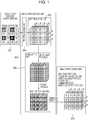
- Fig. 1 illustrates a configuration of an imaging apparatus, an image processing unit 203 provided externally to the imaging apparatus, and signal processing to be performed by the imaging apparatus.
- the imaging apparatus has an image pickup element 201, and a signal processing unit 202.
- the signal processing unit 202 has a pre-processing unit 204, an interpolating unit 205, and a converting unit 206.
- the signal processing unit 202 generates data acquired by performing interpolation processing and an up conversion process on an output signal output from the image pickup element 201.
- the signal processing unit 202 further performs a mosaic process which generates a mosaic image on the data and outputs the resulting data to the image processing unit 203.
- Predetermined data to be input to the image processing unit 203 have a Bayer pattern in this embodiment.
- FIG. 1 also illustrates data sets to be generated by the interpolating unit 205, the converting unit 206, and the image processing unit 203.
- Fig. 1 illustrates data sets generated as a result of the processes performed by those component units.
- the data set illustrated along with the image processing unit 203 is generated as a result of a demosaic process performed by the image processing unit 203 on the data output from the converting unit 206.
- the image pickup element 201 may be a CMOS image sensor or a CCD image sensor, for example. According to this embodiment, a CMOS image sensor is used.
- the image pickup element 201 has a plurality of pixels.
- Each of the plurality of pixels has a light transmission unit. Partial pixels of the plurality of pixels have color filters (CF) each of which allows light having a wavelength corresponding to one of red (R), green (G), and blue (B) colors to pass through.
- the color filters are examples of the light transmission unit.
- Each of the plurality of pixels has a photoelectric converting unit which generates an electric carrier based on incident light.
- a pixel provided for generating an electric carrier based on incident light will be called an effective pixel, hereinafter.
- the number of effective pixels provided in the image pickup element 201 is equal to 1920 pixels in a horizontal direction and 1080 pixels in a vertical direction.
- Fig. 1 illustrates pixels R, G, B, and W in the image pickup element 201.
- the letters “R”, “G”, “B”, and “W” given to the pixels in Fig. 1 indicate colors corresponding to wavelengths of light passing through the light transmission units in the pixels.
- the letters “R”, “G”, “B”, and “W” indicate red, green, blue, and white, respectively.
- the light transmission unit in a W pixel may be a resin which does not have a member configured to narrow the wavelength band range of light passing therethrough. In other words, a W pixel does not have a CF. Therefore, the wavelength band range of light to be received by the photoelectric converting unit in a W pixel is wider than the wavelength band range of light to be received by photoelectric converting units in RGB pixels.
- the image pickup element 201 has a CF pattern called an RGBW12 pattern.
- An arrangement pattern of light transmission units in a plurality of pixels will be called a CF pattern though each W pixel does not have a CF.
- RGBW12 pattern color pixels including red pixels, green pixels, and blue pixels are adjacent to a W pixel in a vertical direction, a horizontal direction, and a diagonal direction in planar view.
- color pixels being a first pixel are adjacent to a W pixel in an upward direction, a downward direction, a right direction, a left direction, an upper right diagonal direction, a lower left diagonal direction, an upper left diagonal direction, and a lower right diagonal direction as seen in a planar view.
- a first direction refers to a direction viewed from a W pixel adjacent to the first pixel in the upper direction to the first pixel in planar view.
- a second direction refers to a direction viewed from a W pixel adjacent to the first pixel in the left direction in planar view to the first pixel.
- a third direction refers to a direction viewed from a W pixel adjacent to the first pixel in the upper right diagonal direction in planar view to the first pixel.
- a fourth direction refers to a direction viewed from a W pixel adjacent to the first pixel in the upper left diagonal direction in planar view to the first pixel.
- the color pixel being the first pixel is surrounded by the plurality of W pixels.
- a pixel A of the plurality of W pixels is a pixel adjacent to the first pixel in the upper direction in planar view.
- a pixel B of the plurality of W pixels is a pixel adjacent to the first pixel in the downward direction in planar view.
- the direction from the pixel A to the pixel B corresponds to the first direction. In the first direction, the first pixel positions between the pixel A and the pixel B.
- a pixel C of the plurality of W pixels is a pixel adjacent to the first pixel in the left direction in planar view.
- a pixel D of the plurality of W pixels is a pixel adjacent to the first pixel in the right direction in planar view. The direction from the pixel C to the pixel D corresponds to the second direction. In the second direction, the first pixel positions between the pixel C and the pixel D.
- a pixel E of the plurality of W pixels is a pixel adjacent to the first pixel in the upper right diagonal direction in planar view.
- a pixel F of the plurality of W pixels is a pixel adjacent to the first pixel in the lower left diagonal direction in the planar view. The direction from the pixel E to the pixel F corresponds to the third direction.
- a pixel G of the plurality of W pixels is a pixel adjacent to the first pixel in the upper left diagonal direction in planar view.
- a pixel H of the plurality of W pixels is a pixel adjacent to the first pixel in the lower right diagonal direction in planar view.
- the direction from the pixel G to the pixel H corresponds to the fourth direction.
- the pixel C and the pixel F are adjacent in the direction parallel to the first direction.
- the pixel A and the pixel E are adjacent in the direction parallel to the second direction.
- the pixels A to H will be called second to ninth pixels, respectively.
- the RGBW12 pattern has a ratio of W pixels equal to 3/4 of the total number of pixels.
- the image pickup element 201 may have a pixel from which an image is not directly output, such as an optical black pixel, and a dummy pixel, in addition to effective pixels.
- Each of the W pixels does not have a CF.
- the wavelength band range to which the W pixels are sensitive may include all wavelength band ranges to which the red pixels, green pixels, and blue pixels are sensitive. Therefore, W pixels have a wider spectral response than that of RGB pixels and have higher sensitivity than those of RGB pixels.
- RGBW12 pattern may improve the precision of interpolation because a color pixel is surrounded by W pixels.
- the signal processing unit 202 performs signal processing on an output signal from the image pickup element 201.
- the signal processing unit 202 has the pre-processing unit 204, the interpolating unit 205, and the converting unit 206.
- An output signal from the image pickup element 201 is input to the pre-processing unit 204 in the signal processing unit 202.
- the pre-processing unit 204 may perform a correction process such as an offset correction and a gain correction on a signal.
- the interpolating unit 205 performs interpolation processing on data output from the pre-processing unit 204.
- the interpolating unit 205 performs a demosaic process.
- the demosaic process according to this embodiment is performed based on a bilinear method for obtaining R data, G data, and B data from signals output from RGB pixels.
- the demosaic process according to this embodiment for R data interpolates with an R component being a value estimated as being obtained when a red pixel positions at a position where a W pixel actually positions.
- the demosaic process of this embodiment interpolates with a B component and a G component, like the R component, to generate B data and G data, respectively.
- the RGBW12 pattern has more W pixels per unit area from which resolution information can be obtained, compared with a case where W pixels are arranged in a checkered pattern.
- resolution information with a higher spatial frequency (or at finer pitches) can be obtained, compared with a case where W pixels are arranged in a checkered pattern.
- the signal processing unit 202 can use output signals output from the image pickup element 201 in the RGBW12 pattern to generate data with a higher sense of resolution than an output signal from an image pickup element in which W pixels are arranged in a checkered pattern.
- the converting unit 206 performs an up conversion process and a mosaic process by using data output from the interpolating unit 205.
- the up conversion process is a resolution increasing process which generates data of a second resolution higher than a first resolution from data of the first resolution.
- an output signal from the image pickup element 201 has a resolution of 1920 ⁇ 1080 pixels, that is, so-called 2K1K resolution.
- the signal processing unit 202 Based on 2K1K input data, the signal processing unit 202 outputs data of 3840 ⁇ 2160 pixels, that is, so-called 4K2K resolution as a result of the up conversion process.
- the converting unit 206 uses one pixel signal output from the interpolating unit 205 to perform processing for generating four pixel signals.
- the up conversion process may be performed by using a nearest neighbor interpolation, a bilinear method, or a bicubic method, for example.
- the converting unit 206 of this embodiment performs a mosaic process, which will be described below, after the up conversion process.
- a nearest neighbor interpolation may be used to prevent accumulation of data processing errors.
- the converting unit 206 of this embodiment performs a mosaic process.
- the mosaic process to be performed by the converting unit 206 of this embodiment is a process for generating Bayer data by using color data of R data, G data, and B data.
- the Bayer data refer to data obtained when RGB pixels are arranged in a Bayer pattern in a single image sensor.
- the image processing unit 203 generates a photographed image by using data output from the signal processing unit 202.
- the image processing unit 203 may perform a demosaic process, a color matrix operation, a white balance process, a digital gain, a gamma process, a noise reduction process, or the like as required. Among these processes, the demosaic process is more greatly associated with the resolution information of the photographed image than the other processes.
- the converting unit 206 performs the mosaic process after performing the up conversion process.
- the image processing unit 203 generates one R signal of R data.
- the image processing unit 203 can generate signals for G data and B data of other colors by performing the same process as the process for generating R data.
- the interpolating unit 205 interpolates signals from the pre-processing unit 204.
- the RGBW12 pattern having more W pixels for obtaining resolution information advantageously provides that data at a resolution with a high spatial frequency (or at fine pitches) can be obtained, compared with W pixels arranged in a checkered pattern.
- correlations in the vertical direction, the horizontal direction and diagonal direction in planar view can be obtained for each pixel.
- correlation directlyivity
- the correlation may be a slope acquired by dividing the difference by a distance between centers of gravity of pixels.
- Examples of the correlation (directivity) may include a result of determination of whether an edge of a photographic subject exists or not or whether an isolated point exists or not. A case where the correlation is acquired by using a difference between signals of a plurality of pixels will be described below.
- the interpolation value may be calculated with reference to data in a direction with higher correlation (or a small difference).
- the value of W at the red pixel can be interpolated with higher precision compared with a case where the interpolation value is calculated with reference to data in a direction with low correlation (or a large difference).
- the directivity calculation process may further include a process for acquiring a distribution. Calculation and interpolation of a correlation value in each direction for deriving correlation will be described in detail below.
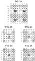
- Figs. 2A to 2E illustrate a method for detecting correlations (directivities) between the RGBW12 pattern and a blue pixel.
- Fig. 2A specifies addresses for pixels.
- a pixel here is represented by a CF color (X coordinate value, Y coordinate value).
- X 3
- a method for acquiring a correlation (directivity) by using an extracted 5 pixel ⁇ 5 pixel region about B(3, 3) will be described.
- the correlation values are calculated based upon directivity.
- Fig. 2B illustrates arrows indicating pixels to be used for calculation of correlation values in the horizontal direction.
- Correlation Value horizontal
- Fig. 2C illustrates arrows indicating pixels to be used for calculation of correlation values in the vertical direction.
- Correlation Value vertical
- Fig. 2D illustrates arrows indicating pixels to be used for calculation of correlation values in the left diagonal direction.
- Each of differences is weighted with its corresponding distance, and a sum total of absolute values of the differences is acquired as the correlation value (left diagonal).
- Correlation Value left diagonal
- Fig. 2E illustrates arrows indicating pixels to be used for calculation of correlation values in the right diagonal direction.
- Each of differences is weighted with its corresponding distance, and a sum total of absolute values of the differences is acquired as the correlation value (right diagonal).
- Correlation Value right diagonal
- the sum of the coefficients of the terms of the differences is equal to 8.
- the coefficients are given for the purpose of reduction of the distance for weighting about the position where the differences are calculated and for the purpose of equalization of weights given to the four correlation values.
- the positions (indicated by arrows) where differences are calculated are arranged linear symmetrically about B(3, 3). This is for improving the symmetrical property for acquiring the correlation values so as to reduce errors relating to correlation values.
- a difference between pixels in proximity of a pixel of interest is multiplied by 2, and a difference between pixels farther from the pixel of interest than the pixels in proximity is one time. Weighting the difference based on a distance from a pixel of interest as described above can increase the precision of the calculated correlation value.
- the direction having the smallest value of the four acquired correlation value can have a small difference, that is, high correlation.
- Fig. 3A illustrates a light exposure pattern of an image sensor in a case where an image having a small correlation value (horizontal) is generated. More specifically, Fig. 3A schematically illustrates signal intensity of data corresponding to pixels in a case where a line extending in a horizontal direction is exposed by an image sensor.
- Fig. 3B illustrates signal intensity in a case where the image in Fig. 3A is captured by using an RGBW12 pattern.
- the "?” in Fig. 3B indicates a pixel (R, G, B) of a color excluding W, and a pixel indicated by W is a W pixel.
- the shading of the W pixels in Fig. 3B indicates signal intensity of data.
- the pixels indicated by "?” are pixels excluding W pixels.
- the interpolation value for the coordinates (3, 3) may be acquired by averaging the data of W(2, 3) and W(4, 3).
- the interpolating unit 205 having the signal processing unit 202 as described above compares correlation values in different directions of W pixels in vicinity of the pixel of interest (3, 3) and acquires a direction with a small difference as a result of the comparison.
- the interpolating unit 205 uses the interpolation direction acquired as a result of the comparison to estimate and interpolate W data of the pixel of interest (3, 3) from the W pixels adjacent to the pixel of interest (3, 3). Performing an interpolation in this way can lead interpolation processing based on information regarding a difference between pixels and can improve the resolution.
- the interpolation for the pixel is indicated by "! at coordinates (3, 3) in Fig. 3C .
- acquiring correlation values also involves acquiring correlation values by using signals between W pixels positioned with a pixel of another color therebetween as illustrated in Fig. 3E .
- the following correlation values in the horizontal direction and the vertical direction may not be equal.
- Correlation Value horizontal
- Correlation Value depth
- the thin line with pixels having an equal correlation value cannot be identified as a vertical line or a horizontal line, an interpolation error may occur. In other words, a pattern of a photographic subject with a small sampling period for W pixels is difficult to detect.
- a correlation value can be acquired by using information regarding a photographic subject, such as edge information and shape information of a photographic subject to acquire the directivity with higher precision. In this case, a sharper image (or an image with higher resolution) can be acquired in this case, compared with a case where interpolation processing is performed by using a correlation value acquired without using information regarding a photographic subject.
- the interpolation values for other colors can be obtained with high precision for a pixel of one color (such as a red pixel). In other words, occurrence of the false color can be reduced.
- a characteristic that a local color change is strongly correlated with a change in brightness is used to acquire a RGB data ratio and a W data ratio of a plurality of pixel data, and the ratios are multiplied by W data.
- the interpolation is performed with color data equivalent to the resolution of W pixels.
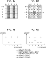
- the interpolation processing will be described with reference to Figs. 4A to 4D .
- Fig. 4A illustrates signal intensity in a case where green-blue lines extending in a vertical direction are exposed to an image sensor.
- Fig. 4B is a graph illustrating the intensity distribution in Fig. 4A against coordinates in an X direction. Because the brightness and darkness of the green-blue lines are repeated alternately, the pattern of the repetition of the brightness and darkness is exposed to W pixels and is converted to data. A case will be described in which the line pattern is exposed with an RGBW12 pattern illustrated in Fig. 4C.
- Fig. 4D plots intensities of W pixels at W(2, 3) and W(4, 3) as indicated by solid line circles, as in explanatory notes.
- Fig. 4B is a graph illustrating the intensity distribution in Fig. 4A against coordinates in an X direction. Because the brightness and darkness of the green-blue lines are repeated alternately, the pattern of the repetition of the brightness and darkness is exposed to W pixels and is converted to data. A case will be described in which the line pattern is exposed with
- FIG. 4D illustrates broken line circles indicating intensity predicted values of interpolated W at coordinates (1, 3), (3, 3), and (5, 3) and exhibiting iWg(1, 3), iWb(3, 3), and iWg(5, 3). These values are inferred as data equivalent to W(3, 2) and W(3, 4) because the pattern has vertical thin lines.
- a change in blue color in the neighborhood can be expressed by multiplying the color ratio B(3, 3)/iWb(3, 3) by data of W.
- the color ratio can correct the false color by using iWb(3, 3) with high precision.
- iWr is a W interpolation value for a red pixel
- iWgr is a W interpolation value for Gr pixel
- iWgb is a W interpolation value for a Gb
- iWb is a W interpolation value for a blue pixel.
- RGB _ ratio R R iWr + Gr + Gb iWgr + iWgb + B iWb Gr + Gb 2 R iWr + Gr + Gb iWgr + iWgb + B iWb B R iWr + Gr + Gb iWgr + iWgb + B iWb
- RGB _ ratio R _ ratio G _ ratio B _ ratio
- RGB image having undergone the interpolation and the false color correction can be formed from RGBW12 data.
- the converting unit 206 performs up conversion and remosaic processes by using a signal from the interpolating unit 205.
- the up conversion process is a type of resolution conversion and collectively refers to generating an image with a higher resolution than an original resolution.
- the image processing unit 203 is a part which uses an output from the signal processing unit 202 to generate an output image and may also be called a RGB signal processing unit because it may generate an RGB image.
- the image processing unit 203 converts an output from a sensor to a color image by performing a demosaic process, a color matrix operation, a white balance process, a digital gain, a gamma process, a noise reduction process, and the like as required.
- the demosaic part is particularly important to resolution information, and advanced interpolation processing can be performed by assuming CFs in a Bayer pattern from it.
- Manufacturing a new dedicated image processing unit for an image pickup element having a special CF pattern may result in increases of costs and time. Therefore, use of an image processing unit configured to process a general Bayer pattern may be highly advantageous. Thus, performing the remosaic process as described above enables use of the special CF pattern at low cost.
- FIG. 1 An imaging apparatus according to a first exemplary embodiment will be described with reference to drawings. The following descriptions may refer to the imaging apparatus in Fig. 1 as required.
- FIG. 5 illustrates an example of an image pickup element 201 according to this exemplary embodiment.
- An image pickup element 201 according to this exemplary embodiment has an image sensing region 1 having a pixel array having pixels 100 arranged in a matrix form, a vertical scanning circuit 2, a columnar amplifying unit 3, a horizontal scanning circuit 4, and an output unit 5.
- the vertical scanning circuit 2 supplies a control signal for controlling an ON state (conductive state) and an OFF state (non-conductive state) of transistors in the pixels 100 to the transistors of the pixels 100.
- the image sensing region 1 has a vertical signal line 6 for reading out signals from the pixels 100 column by column.
- the horizontal scanning circuit 4 has a switch for the columnar amplifying unit 3 for the columns and a horizontal scanning circuit 4 configured to supply a control signal for controlling the switch to an ON state or an OFF state.
- signals are sequentially output from columns associated with the columnar amplifying unit 3 to the output unit 5.
- the signals output from the columnar amplifying unit 3 to the output unit 5 are input to a signal processing unit 202 external to the image pickup element 201, as illustrated in Fig. 1 .
- output signals output from the image pickup element 201 are analog signals, for example, the image pickup element 201 may output digital signals. In that case, an analog-digital conversion process to be performed by the signal processing unit 202 may be omitted.
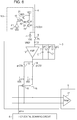
- the imaging apparatus in Fig. 5 will be described with reference to Fig. 6 .
- the vertical scanning circuit 2 controls signal levels of a signal PTX, a signal PRES, and a signal PSEL to be supplied to the pixels 100 to perform vertical scanning which is scanning pixels 100 in the image sensing region 1 row by row.
- each of the pixels 100 outputs a photoelectric conversion signal to a vertical signal line 6 through a PDOUT terminal.
- a current source 7 supplies electric current to the pixels 100 through the vertical signal line 6.
- a switch 8 controls an input to the columnar amplifying unit 3.
- the columnar amplifying unit 3 has a capacitance C0, a capacitance C1, a capacitance C2, a switch 9, a switch 10, a switch 11, and an amplifying circuit 12 for determining the amplification efficiency of the columnar amplifying unit 3.
- the columnar amplifying unit 3 has a switch 13, a switch 14, a storage capacitor CTN, and a storage capacitor CTS for sample holding and a switch 15, and a switch 16 for connecting to a horizontal transfer signal line.
- the horizontal scanning circuit 4 sequentially controls conductive states and non-conductive states of the switch 15 and the switch 16 for columns for which the amplifying circuit 12 is provided. Thus, the horizontal scanning circuit 4 performs horizontal scanning which is scanning column by column to be performed by the columnar amplifying unit 3.
- An output amplifier 17 outputs signals acquired by amplifying input signals externally to the image pickup element.
- Each of the pixels 100 has a photodiode 18, a transistor 19, a floating diffusion capacitance 20, a transistor 21, a transistor 22, and a transistor 23.
- a photodiode (hereinafter, sometimes called a PD) 18 is a photoelectric converting unit configured to accumulate electric carriers based on incident light.
- the transistor 19 has one terminal connected to the photodiode 18 and the other terminal connected to the floating diffusion capacitance 20.
- the floating diffusion capacitance (sometimes called an FD) 20 is a structure also functioning as a drain terminal of the transistor 19 and is capable of holding electric carriers transferred (sometimes called a TX) from the photodiode 18 through the transistor 19.
- the electric carriers accumulated in the photodiode 18 are transferred when a signal PTX input from the vertical scanning circuit 2 to a gate terminal of the transistor 19 is changed to a High level (sometimes called an H level).
- the transistor 21 When the signal PRES input from the vertical scanning circuit 2 is changed to an H level, the transistor 21 resets (sometimes called RES) the potential of the floating diffusion capacitance 20 to a potential based on power supply voltage VDD.
- the transistor 22 has an input node electrically connected to the floating diffusion capacitance 20.
- the transistor 22 has one main node receiving supply of bias electric current from the current source 7 connected through the vertical signal line 6 and the other main node receiving supply of power supply voltage VDD so that a source follower (sometimes called an SF).
- a source follower sometimes called an SF
- the transistor 23 When a signal PSEL input from the vertical scanning circuit 2 is changed to an H level, the transistor 23 outputs a signal output from the transistor 22 to the vertical signal line 6. The transistor 23 outputs a signal to the vertical signal line 6 at a node PDOUT. A signal output from the transistor 22 is based on electric carriers held in the floating diffusion capacitance 20.
- the switch 8 controls so as to input a signal output from the corresponding pixel 100 to the amplifying circuit 12.
- the capacitance C0, the capacitance C1, and the capacitance C2 are capacitances usable for amplification to be performed by the amplifying circuit 12.
- the switch 9, and the switch 10 are controlled such that input voltage can be amplified in accordance with a capacitance ratio of C0/C1, C0/C2, or C0/(C1 + C2).
- the switch 11 is usable for controlling the resets of the capacitance C1 and the capacitance C2.
- the switch 13 and the switch 14 are controlled such that a signal output from the amplifying circuit 12 can be sample-held in the capacitances CTN and CTS.
- the switch 13 is turned on so that an output signal (sometimes called an N signal) when the floating diffusion capacitance 20 has a reset level among signals output from the pixel 100 can be sample held in the capacitance CTN.
- the switch 14 is turned so that an output signal (sometimes called an S signal) when electric carriers are transferred to the floating diffusion capacitance 20 among output signals from the pixel 100 can be sample held in the capacitance CTS.
- the switch 15 and the switch 16 are controlled such that a signal ⁇ Hn from the horizontal scanning circuit 4 can be changed to an H level and outputs of the sample-held capacitance CTN and capacitance CTS are sequentially connected to the output amplifier 17.
- the image pickup element as described above may be used so that an optical signal input to the image pickup element can be read out as an electric signal.
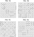
- Figs. 7A to 7D illustrate examples of a CF pattern using RGB pixels as color pixels.
- Fig. 7A illustrates a Bayer pattern having a CF ratio of R:G:B equal to 1:2:1. More green pixels are provided than pixels of other colors because visual properties of a human being is highly sensitive to the G wavelength, and more green pixels can give a sense of resolution.
- a green pixel is adjacent to a red pixel or a blue pixel in an upper direction, a downward direction, a right direction, and a left direction in planar view.
- a green pixel is adjacent to another green pixel in upper right diagonal, lower right diagonal, upper left diagonal, and lower left diagonal directions in planar view.
- a red pixel is adjacent to a blue pixel in upper right diagonal, lower right diagonal, upper left diagonal, and lower left diagonal directions in planar view.
- pixel data between green pixels having a pixel of another color therebetween is used for calculating the correlation values for the upward, downward, right and left directions.
- pixel data of adjacent pixels of different colors may be used. This may reduce the precision of calculation of the correlation values, and false color may easily occur.
- Fig. 7C illustrates an RGBW8 pattern.
- RGB pixels are arranged adjacently to a W pixel in upward, downward, right and left directions in planar view.
- the RGB pixels are arranged adjacently to pixels of different colors from a W pixel in upper right diagonal, lower right diagonal, upper left diagonal, and lower left diagonal directions in planar view.
- the precision of calculation of correlation values can be reduced, and false color may easily occur, like the Bayer pattern in Fig. 7A as described above.
- Fig. 7B illustrates a RGBW12 pattern.
- the pattern includes a characteristic that all of RGB pixels being color pixels are surrounded by W pixels.
- the term "surrounded” refers to a W pixel is disposed in all directions of upward, downward, right and left, upper right diagonal, lower right diagonal, upper left diagonal, lower left diagonal directions about a pixel of interest in planar view.
- the proportion of W pixels is equal to 3/4 of all effective pixels.
- interpolation processing with high precision can be achieved by using an image pickup element having the RGBW12 pattern.
- the RGBW12 pattern has more W pixels than those of the Bayer pattern and the RGBW8 pattern, which can provide an effect for improving the sensitivity of the image pickup element 201.
- Fig. 7D illustrates a CF pattern called an RGBG12.
- This pattern is defined such that a red pixel and a blue pixel are surrounded by green pixels, and the proportion of the green pixels is equal to 3/4 of all of the pixels.
- Each of red pixels and blue pixels is adjacent to a green pixel in the upward, downward, right, left, upper right diagonal, lower right diagonal, upper left diagonal, and lower left diagonal directions. In other words, each of red pixels and blue pixels is surrounded by green pixels.
- correlation values in the vertical, horizontal, right diagonal, and left diagonal directions can be acquired by using pixel data of two or more adjacent green pixels, like the case with the RGBW12 pattern in Fig. 7B as described above. Therefore, interpolation processing with high precision can be achieved by using an image pickup element having the RGBG12 pattern.
- a brightness value at a high resolution can be obtained at all pixel positions where the value of a green pixel is equal to the value of brightness.
- the proportion of green pixel with higher sensitivity to red pixels and blue pixels is higher, which can improve sensitivity of the RGBG pattern more than the Bayer pattern.
- Figs. 8A to 8D illustrate examples of pixel patterns where CFs of complementary colors of C (cyan), M (magenta), and Y (yellow).
- Fig. 8D illustrates a CMYY12 pattern.
- the interpolation processing of this embodiment can be performed properly, as in the cases illustrated in Figs. 7A to 7D .
- the interpolation processing of this embodiment can be performed properly in the patterns illustrated in Figs. 8B and 8D .
- the CFs can be arranged in various patterns.
- more pixels which generate resolution data green pixels in a Bayer pattern, and W pixels in an image pickup element having W pixels
- Green pixels which generate resolution data may be arranged in a checkered pattern as a Bayer pattern, which may cause an interpolation error.
- more pixels which generate resolution data are provided than those in the checkered pattern, from which occurrence of smaller interpolation error has been found. Therefore, the effect of the present invention may be exhibited significantly by using an image pickup element having a CF pattern such as the RGBW12 in Fig. 7B , the RGBG12 in Fig.
- the interpolating unit 205 can perform interpolation with high precision.
- the interpolating unit 205 can obtain a brightness value at the color pixel position with high precision.
- a plurality of brightness pixels which generate brightness arranged at four sides of a color pixel which generates color and a plurality of brightness pixels which share four apexes of the color pixel are arranged.
- brightness information at the color pixel position can be obtained through interpolation with high precision.
- each of the pixels is rectangular, and brightness pixels which generate brightness are adjacent to each of the pixels in eight directions of upward, downward, right, left, upper right diagonal, lower right diagonal, upper left diagonal, and lower left diagonal directions.
- the present invention is not limited thereto but may be applied to a case where each of the pixels may be hexagonal brightness pixels are arranged adjacently to six sides of the hexagon. Also in this case, correlation values in four directions of vertical direction, horizontal direction, right diagonal direction, and left diagonal directions may be acquired by using pixel data of adjacent two pixels of an identical color, and the correlation values may be compared to obtain information regarding differences between them.
- the interpolation processing according to this embodiment can be performed properly.
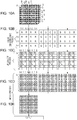
- Figs. 9A to 9E illustrate processes to be performed by the interpolating unit 205 illustrated in Fig. 1 . It should be noted that Figs. 9A to 9E illustrate a case where the image pickup element 201 has an RGBW12 pattern as a CF pattern.
- Fig. 9A illustrates data to be input from the pre-processing unit 204.
- the pre-processing unit 204 may perform a correction process such as an offset (OFFSET) correction and a gain (GAIN) correction on an input signal Din as required to generate an output Dout having undergone the correction process.
- the process may typically be expressed by the following expression (5).
- Dout Din ⁇ OFFSET ⁇ GAIN
- This correction may be performed in various units. For example, the correction may be performed on each pixel, each columnar amplifier, each analog-digital converting unit(ADC), or each output amplifier. Performing the correction may reduce so-called fixed pattern noise and can provide a higher quality image.
- ADC analog-digital converting unit
- the interpolating unit 205 performs a "data demultiplexing" process which demultiplexes data output from the pre-processing unit 204 into W data and color data (of a G signal, an R signal, and a B signal).
- the signal of a pixel of RGB pixels in 4 ⁇ 4 pixels from which W data are obtained is not known (indicated by "?" in drawings) as illustrated in Fig. 9B .
- the color data have a low resolution (spatially coarse) because they are obtained from 2 ⁇ 2 pixels of 4 ⁇ 4 pixels, as illustrated in Fig. 9D .
- the interpolating unit 205 performs a process for interpolating the signal indicated by "?" by using surrounding signals.
- the interpolation process may be performed based on any of various methods.
- the methods may include a method (bilinear method) which averages signals of upper, lower and right and left four pixels to average signals of surrounding eight pixels, a method which detects edges of surrounding pixels and performs an interpolation process perpendicularly to the edge directions, and a method which detects a pattern of thin lines, for example, and performs an interpolation process in the direction of the pattern.
- the interpolation process may be performed based on the following method.
- Fig. 9C also illustrates X coordinates and Y coordinates.
- a signal iWb is a signal having coordinates (3, 3) in W data and is therefore indicated as iWb (3, 3).
- iWb is unknown when the signal is input, an interpolation is necessary.
- iWb(3, 3) can be acquired by Expression (6) below.
- iW b 3 3 W 2 2 + W 3 2 + W 4 2 + W 2 3 + W 4 3 + W 2 4 + W 3 4 + W 4 + W 4 4 8
- a signal of a pixel having an unknown signal value is interpolated with signal values of surrounding pixels.
- a 4 ⁇ 4 pixel array is illustrated but iWr and iWg can be interpolated with information regarding surrounding eight pixels because the same pattern as illustrated is repeated.
- the interpolating unit 205 generates color data of R data, G data, and B data by using the interpolated W data as well as extracted color data.
- Colors to be used for generating R data, G data, and B data may be calculated based on various methods. As an example, color data may be standardized to acquire a ratio of colors. According to this method, a ratio of colors can be calculated by the following expression (7).
- RGB _ ratio R R + G + B G R + G + B B R + G + B
- RGB _ ratio R iWr Gr + Gb iWgr + iWgb B iWb
- the method for acquiring the ratio of color data and interpolated iWr*iWgr*iWgb*iWb is applied.
- RGB_ratio being the ratio of colors and a W signal or a signal of the interpolation value iWr*iWgr*iWgb*iWb may be used to acquire signal values corresponding to colors of R, G, and B at the pixels as in Expression (10).
- RGB R _ ratio ⁇ W G _ ratio ⁇ W B _ ratio ⁇ W
- RGB _ ratio R _ ratio G _ ratio B _ ratio is satisfied, and the calculated color data are also used.
- the R data, G data, and B data generated by the interpolating unit 205 are first data generated by synthesizing resolution data and color data.
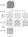
- Figs. 10A to 10E illustrate signal processing including performing an up conversion process and a mosaic process on color data and outputting Bayer data.
- Fig. 10A illustrates data input from the interpolating unit 205.
- the data are demultiplexed into R data, G data, and B data as illustrated in Fig. 10B .
- the color-demultiplexed color data undergo an up conversion process to have double resolutions in a vertical direction and a horizontal direction.
- Fig. 10B, Fig. 10C, and Fig. 10D also illustrate X coordinates and Y coordinates.
- R(1, 1) in Fig. 10C is directly associated with the pixel at R(1, 1) in Fig. 10B .
- All of the pixels (1, 2), (2, 1), and (2, 2) in Fig. 10C have unknown signal values.
- nearest neighbor interpolation is used for interpolating an unknown signal value. The method assumes that the signal values of (2, 1), (1, 2), and (2, 2) in Fig. 10C are equal to the value of R(1, 1).
- R data, G data, and B data having resolutions improved twice in the vertical direction and the horizontal direction are generated.
- the data acquired by the up conversion process are second data acquired by performing the up conversion process on the first data generated by the interpolating unit 205.
- shaded pixels in Fig. 10D are extracted.
- R data in Fig. 10D a signal having a lowest X coordinate value and a lowest Y coordinate value among signals of each array of 2 ⁇ 2 pixels is used. That is, signals at R(1, 1), R(3, 1), R(5, 1), R(7, 1), R(3, 1) and so on are used.
- G data data in a checkered pattern are extracted, like data in a Bayer pattern.
- B data a signal having a lowest X coordinate value and a lowest Y coordinate value among signals of each array of 2 ⁇ 2 pixels is used. That is, signals at B(2, 2), B(4, 2), B(6, 2), B(8, 1), B(4, 2)and so on are used.
- the converting unit 206 acquires mosaic data illustrated in Fig. 10E .
- the converting unit 206 outputs the mosaic data to the image processing unit 203.
- the mosaic data are data to be used for generating an image by the image processing unit 203.
- the data to be input to the image processing unit 203 are arranged in a Bayer pattern.
- the image processing unit 203 performs the operations described with reference to Fig. 1 .
- the image processing unit 203 generates a photographed image of a photographic subject.
- An evaluation photographing has been performed by using an imaging apparatus configured to perform the processing as described above.
- a TV resolution has been evaluated by using a resolution chart.
- mosaic data are generated by causing the converting unit 206 to perform the processing in Figs. 10A to 10E except for the up conversion process, as illustrated in Fig. 13A to 13D .
- the mosaic data are used to generate a photographed image by the image processing unit 203.
- the photographed image acquired by performing the processing as illustrated in Figs. 10A to 10E according to this exemplary embodiment have 1000 TV horizontal resolutions.
- the photographed image according to the other example has 900 TV horizontal resolutions. Therefore, the image acquired by performing the up conversion process and thus generating mosaic data can have a better resolution.
- the number of pixel signals may be equal to the number of pixels of the image pickup element 201 or may be equal to pixels in a limited region for outputting signals in the image pickup element 201 (which may be called partial readout or crop) or may be equal to the sum of signals added within the image pickup element 201 (which may be called binning). Thus, a pixel signals less than the number of pixels of the image pickup element 201 may be output.
- the effect of the processing according to this exemplary embodiment can be achieved by performing the up conversion process on output pixel signals and not depend on the total number of pixels of the image pickup element 201.
- Each of the signal processing unit 202 and the image processing unit 203 in this exemplary embodiment may be an integrated circuit mounted on a semiconductor substrate.
- the imaging apparatus of this exemplary embodiment may apply a stacked sensor in which a semiconductor substrate having the signal processing unit 202 thereon and a semiconductor substrate having the image pickup element 201 thereon are stacked.
- the image processing unit 203 is provided externally to the imaging apparatus.
- the imaging apparatus may contain the image processing unit 203.
- RGB data may be output from the signal processing unit 202 to an image processing unit, or video data may be output directly from the signal processing unit 202.
- Evaluation photographing was performed by using the imaging apparatus having performed the processing above.
- the subject image was evaluated based on a TV resolution for acquiring the sense of resolution.
- the TV resolution is acquired by using pixel data of pixels of a first color having a pixel of a second color therebetween for detection of the directivity.
- the precision of the directivity calculation is lower than that of this exemplary embodiment. Because no column or row having adjacent pixels of the first color exists in the comparison examples, the precision of detection of a linear photographic subject is lower than that of this exemplary embodiment. From this, the precision of detection of the directivity in the linear photographic subject in the comparison example is lower than that of this exemplary embodiment.
- the output data of this embodiment has 1000 TV horizontal resolutions.
- the output data of the comparison example has 900 TV horizontal resolutions.
- the signal processing of this embodiment may be performed by the image processing unit 203 configured to process an output signal output from the image pickup element 201 having RGB pixels in a Bayer pattern, instead of the image pickup element 201 having W pixels as in this embodiment. Therefore, the signal processing of this embodiment can reduce costs for designing the image processing unit 203 specially for the image pickup element 201 having W pixels. In other words, the signal processing of this embodiment can suppress the compatibility between the imaging apparatus and the image processing unit 203. Therefore, the signal processing of this embodiment can generate a photographed image having reduced color noise while suppressing the compatibility between the imaging apparatus and the image processing unit 203.
- the signal processing unit 202 and the image processing unit 203 may be implemented by hardware such as a computer caused to execute a software program corresponding to the signal processing method.
- the signal processing method executed by the signal processing unit 202 and the image processing unit 203 of this embodiment may be programmed in software to be distributed in a recording medium such as a CD-ROM and a DVD-ROM or through communication.
- the W data and color data illustrated in Figs. 9B and 9D may be acquired by averaging W data and color data of a plurality of frames output from the image pickup element 201.
- W data of N frames (where N is a number equal to or higher than 1) may be averaged, and color data of M frames more than N frames may be averaged.
- an image having reduced color noise may be generated while suppressing the reduction of the sense of resolution may be suppressed.
- W data of one frame and color data of a plurality of frames may be used to generate the image, without averaging W data. In this case, an image having reduced color noise can be obtained while preventing fluctuations of the photographic subject.
- the image processing unit 203 may average W data and color data of every plurality of frames to generate an image. On the other hand, in a case where it is detected that a moving object is included in a photographic subject, the image processing unit 203 may generate an image from W data and color data of every frame.
- An imaging apparatus according to a second exemplary embodiment will be described mainly with respect to differences from the first exemplary embodiment.
- the imaging apparatus of this exemplary embodiment acquires correlation values by weighting based on distances between pixels to calculate the correlation values.
- Pixels of the image pickup element 201 of this exemplary embodiment are arranged in a two-dimensional grid pattern being substantially square. Therefore, with respect to a pixel of interest to be interpolated, the distance to a pixel to obtain a difference which is adjacent to the pixel of interest in a diagonal direction is larger than the distance to the pixel adjacent to the pixel of interest in a vertical direction.
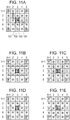
- Figs. 11A to 11E illustrate distances from a pixel of interest to the other pixel to acquire a difference.
- Fig. 11A illustrates a distance from a pixel of interest B(3, 3) to an adjacent pixel to obtain a difference for obtaining a correlation value about the pixel B(3, 3).
- the distance from the center of gravity of the pixel of interest to the center of gravity of the other pixel to obtain a difference is defined as a single calculation distance with reference to the centers of gravity of the two pixels to obtain a difference.
- the term "center of gravity” refers to a position where the center of gravity of one microlens provided for one pixel is projected to a semiconductor substrate having the pixel, for example.
- Another example of the "center of gravity” may be the center of gravity of a photoelectric converting unit if a pixel has one photoelectric converting unit.
- in the vertical direction in Fig. 11A and B(3, 3) is equal to ⁇ 5, where one pixel has a pitch of 2.
- in the vertical direction in Fig. 11A and B(3, 3) is equal to ⁇ 13, where one pixel has a pitch of 2.
- in the diagonal direction in Fig. 11A and the B(3, 3) is equal to ⁇ 2, where one pixel has a pitch of 2.
- in the diagonal direction in Fig. 11A and B(3, 3) is equal to ⁇ 10, where one pixel has a pitch of 2.
- the vertical and horizontal calculation distance is equal to about 17.9, and the calculation distance in the diagonal direction is equal to about 18.3.
- the ratio is about 1.02 times.
- the different calculation distances that is, the different distances from the pixel of interest to a pixel to acquire a difference means that the distances for acquiring a spatial directivity are different.
- the distances are different in the directions for acquiring correlation values, error may occur during detection of the directivity. Therefore, calculation distances as equal as possible may be desirable, and the ratio of the highest value and the lowest value of the calculation distance is preferably equal to or lower than 2.
- the differences from adjacent pixels indicated by arrows in Fig. 11B, Fig. 11C, Fig. 11D, and Fig. 11E are acquired to obtain the correlation values.
- the correlation values may be obtained as follows.
- Correlation Value horizontal
- Correlation Value vertical
- the calculation distance in the vertical and horizontal directions is equal to about 41.26, and the calculation distance in the diagonal directions is equal to about 30.96.
- the ratio is about 1.33 times.
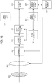
- the imaging system is an apparatus configured to capture an image and a moving picture by using the imaging apparatus and may be a digital still camera, digital camcorder, or a surveillance camera, for example.
- Fig. 12 illustrates a block diagram of an example of the imaging system applying an imaging apparatus according to any one of the first and second exemplary embodiments to a digital still camera.
- the imaging system has a lens 302 causing an optical image of a photographic subject to be focused in the imaging apparatus 301, and a diaphragm 304 usable for adjusting the amount of light passing through a barrier 303 and the lens 302 for protecting the lens 302.
- the imaging system further includes an output signal processing unit 305 configured to process an output signal output from the imaging apparatus 301.
- the output signal processing unit 305 has an image processing unit 203 according to any one of the first and second exemplary embodiments.
- the output signal processing unit 305 is provided on a semiconductor substrate different from a semiconductor substrate having the imaging apparatus 301 thereon.
- the output signal processing unit 305 has a digital signal processing unit configured to perform a correction process and a compression process as required on a signal output from the imaging apparatus 301 and output a resulting signal.
- the imaging system further includes a buffer memory unit 306 configured to temporarily store image data and a storage medium control interface (I/F) unit 307 usable for writing to or reading from a recording medium.
- the imaging system further has a recording medium 309 detachably mounted or built in the imaging system, such as a semiconductor memory, usable for writing or reading captured data.
- the imaging system further has an external interface (I/F) unit 308 usable for communication with an external computer, for example and an overall control/calculation unit 310 configured to control arithmetic operations and the whole digital still camera.
- the imaging system further has a timing generator 311 configured to output a timing signal to the output signal processing unit 305.
- a control signal such as a timing signal may be input externally, instead of the timing generator 311.
- the imaging system may include at least the imaging apparatus 301 and the output signal processing unit 305 configured to process an output signal output from the imaging apparatus 301.
- the imaging system according to this exemplary embodiment is capable of performing imaging operations by applying the imaging apparatus 301 according to any one of the first and second exemplary embodiments.
- Embodiment(s) of the present invention can also be realized by a computer of a system or apparatus that reads out and executes computer executable instructions (e.g., one or more programs) recorded on a storage medium (which may also be referred to more fully as a 'non-transitory computer-readable storage medium') to perform the functions of one or more of the above-described embodiment(s) and/or that includes one or more circuits (e.g., application specific integrated circuit (ASIC)) for performing the functions of one or more of the above-described embodiment(s), and by a method performed by the computer of the system or apparatus by, for example, reading out and executing the computer executable instructions from the storage medium to perform the functions of one or more of the above-described embodiment(s) and/or controlling the one or more circuits to perform the functions of one or more of the above-described embodiment(s).
- computer executable instructions e.g., one or more programs
- a storage medium which may also be referred to more fully as
- the computer may comprise one or more processors (e.g., central processing unit (CPU), micro processing unit (MPU)) and may include a network of separate computers or separate processors to read out and execute the computer executable instructions.
- the computer executable instructions may be provided to the computer, for example, from a network or the storage medium.
- the storage medium may include, for example, one or more of a hard disk, a random-access memory (RAM), a read only memory (ROM), a storage of distributed computing systems, an optical disk (such as a compact disc (CD), digital versatile disc (DVD), or Blu-ray Disc (BD)TM), a flash memory device, a memory card, and the like.
Landscapes
- Engineering & Computer Science (AREA)
- Multimedia (AREA)
- Signal Processing (AREA)
- Physics & Mathematics (AREA)
- Spectroscopy & Molecular Physics (AREA)
- General Physics & Mathematics (AREA)
- Theoretical Computer Science (AREA)
- Color Television Image Signal Generators (AREA)
- Transforming Light Signals Into Electric Signals (AREA)
Claims (11)
- Bildgebungsvorrichtung umfassend:einen ersten Pixel, einen zweiten Pixel, einen dritten Pixel, einen vierten Pixel, einen fünften Pixel, einen sechsten Pixel und einen siebten Pixel, wobei jeder der Pixel (100) eine photoelektrische Umwandlungseinheit (18) sowie eine Signalverarbeitungseinheit (202) aufweist;wobei ein Wellenlängenbandbereich von Licht, das durch die photoelektrische Umwandlungseinheit (18) des ersten Pixels photoelektrisch umgewandelt werden soll, ein erster Wellenlängenbandbereich ist;ein Wellenlängenbandbereich von Licht, das durch die photoelektrische Umwandlungseinheit (18) von jedem der zweiten bis siebten Pixel photoelektrisch umgewandelt werden soll, ein zweiter Wellenlängenbandbereich ist, wobei der zweite Wellenlängenbandbereich den ersten Wellenlängenbandbereich beinhaltet und breiter als der erste Wellenlängenbandbereich ist;die zweiten bis siebten Pixel zum ersten Pixel benachbart sind;der erste Pixel sich in einer ersten Richtung zwischen dem zweiten Pixel und dem dritten Pixel befindet;der erste Pixel sich in einer von der ersten Richtung verschiedenen zweiten Richtung zwischen dem vierten Pixel und dem fünften Pixel befindet;der erste Pixel sich in einer von den ersten und zweiten Richtungen verschiedenen dritten Richtung zwischen dem sechsten Pixel und dem siebten Pixel befindet;der vierte Pixel und der siebte Pixel entlang einer zur ersten Richtung parallelen Richtung benachbart bereitgestellt sind;der zweite Pixel und der sechste Pixel entlang einer zur zweiten Richtung parallelen Richtung benachbart bereitgestellt sind;die Signalverarbeitungseinheit (202) einen ersten Korrelationswert, der ein Korrelationswert in der ersten Richtung ist, aus Signalen des vierten Pixels und des siebten Pixels erfasst, und einen zweiten Korrelationswert, der ein Korrelationswert in der zweiten Richtung ist, aus Signalen des zweiten Pixels und des sechsten Pixels erfasst;die Signalverarbeitungseinheit (202) eine Richtung mit höherer Korrelation zwischen der ersten Richtung und der zweiten Richtung durch Vergleichen des ersten Korrelationswerts und des zweiten Korrelationswerts erfasst; unddie Signalverarbeitungseinheit (202) weiterhin ein dem zweiten Wellenlängenbandbereich des ersten Pixels entsprechendes Signal durch Verwenden von Signalen von zwei Pixeln, die entlang der Richtung mit höherer Korrelation unter den zweiten bis siebten Pixeln bereitgestellt sind, interpoliert.
- Bildgebungsvorrichtung nach Anspruch 1,wobei der erste Pixel weiterhin benachbart zu achten und neunten Pixeln ist, die jeweils eine photoelektrische Umwandlungseinheit (18) aufweisen, die Licht des zweiten Wellenlängenbandbereichs photoelektrisch umwandelt, und der erste Pixel sich in einer von den ersten, zweiten und dritten Richtungen verschiedenen vierten Richtung zwischen dem achten Pixel und dem neunten Pixel befindet;der achte Pixel, der vierte Pixel und der siebte Pixel in einer zur ersten Richtung parallelen Richtung benachbart bereitgestellt sind;der sechste Pixel, der fünfte Pixel und der neunte Pixel entlang einer zur ersten Richtung parallelen Richtung benachbart bereitgestellt sind;der achte Pixel, der zweite Pixel und der sechste Pixel entlang einer zur zweiten Richtung parallelen Richtung benachbart bereitgestellt sind; undder siebte Pixel, der dritte Pixel und der neunte Pixel in einer zur zweiten Richtung parallelen Richtung benachbart bereitgestellt sind,wobei die Signalverarbeitungseinheit (202) erfasst:den ersten Korrelationswert durch Verwenden von Signalen des achten Pixels, des vierten Pixels und des siebten Pixels;den zweiten Korrelationswert durch Verwenden von Signalen des achten Pixels, des zweiten Pixels und des sechsten Pixels;einen dritten Korrelationswert, der ein Korrelationswert in der dritten Richtung ist, durch Verwenden von Signalen des zweiten Pixels und des vierten Pixels; sowieeinen vierten Korrelationswert, der ein Korrelationswert in der vierten Richtung ist, durch Verwenden von Signalen des zweiten Pixels und des fünften Pixels; unddie Signalverarbeitungseinheit (202) eine Richtung mit einer höchsten Korrelation unter den ersten, zweiten, dritten und vierten Richtungen durch Vergleichen der ersten, zweiten, dritten und vierten Korrelationswerte erfasst, und ein dem zweiten Wellenlängenbandbereich des ersten Pixels entsprechendes Signal durch Verwenden von Signalen von zwei Pixeln, die entlang der Richtung mit der höchsten Korrelation unter den zweiten bis neunten Pixeln bereitgestellt sind, interpoliert.
- Bildgebungsvorrichtung nach Anspruch 2,
wobei die Signalverarbeitungseinheit (202) die ersten, zweiten, dritten und vierten Korrelationswerte durch Gewichten basierend auf einem Abstand zwischen einem Schwerpunkt des ersten Pixels und einem Schwerpunkt des zweiten Pixels erfasst. - Bildgebungsvorrichtung nach einem vorstehenden Anspruch,
wobei die Pixel (100) angeordnet sind, um eines der folgenden Muster aufzuweisen:ein RGBW12 Muster;ein RGBG12 Muster;ein CMYW12 Muster; sowieein CMYY12 Muster. - Bildgebungssystem umfassend:die Bildgebungsvorrichtung nach einem der Ansprüche 1 bis 4; sowieeine Bildverarbeitungseinheit (203), die durch Verwenden eines von der Bildgebungsvorrichtung ausgegebenen Signals ein Bild generiert.
- Signalverarbeitungsverfahren zum Verarbeiten von Signalen, die von einem ersten Pixel, einem zweiten Pixel, einem dritten Pixel, einem vierten Pixel, einem fünften Pixel, einem sechsten Pixel und einem siebten Pixel ausgegeben werden, wobei jeder der Pixel (100) eine photoelektrische Umwandlungseinheit (18) aufweist, und wobei:ein Wellenlängenbandbereich von Licht, das durch die photoelektrische Umwandlungseinheit (18) des ersten Pixels photoelektrisch umgewandelt werden soll, ein erster Wellenlängenbandbereich ist;ein Wellenlängenbandbereich von Licht, das durch die photoelektrische Umwandlungseinheit (18) von jedem der zweiten bis siebten Pixel photoelektrisch umgewandelt werden soll, ein zweiter Wellenlängenbandbereich ist, wobei der zweite Wellenlängenbandbereich den ersten Wellenlängenbandbereich beinhaltet und breiter als der erste Wellenlängenbandbereich ist;die zweiten bis siebten Pixel benachbart zum ersten Pixel sind;der erste Pixel sich in einer ersten Richtung zwischen dem zweiten Pixel und dem dritten Pixel befindet;der erste Pixel sich in einer von der ersten Richtung verschiedenen zweiten Richtung zwischen dem vierten Pixel und dem fünften Pixel befindet;der erste Pixel sich in einer von den ersten und zweiten Richtungen verschiedenen dritten Richtung zwischen dem sechsten Pixel und dem siebten Pixel befindet;der vierte Pixel und der siebte Pixel entlang einer zur ersten Richtung parallelen Richtung benachbart bereitgestellt sind;der zweite Pixel und der sechste Pixel entlang einer zur zweiten Richtung parallelen Richtung benachbart bereitgestellt sind;das Signalverarbeitungsverfahren umfasst:Erfassen eines ersten Korrelationswerts, der ein Korrelationswert in der ersten Richtung ist, aus Signalen des vierten Pixels und des siebten Pixels, und Erfassen eines zweiten Korrelationswerts, der ein Korrelationswert in der zweiten Richtung ist, aus Signalen des zweiten Pixels und des sechsten Pixels;Erfassen einer Richtung mit höherer Korrelation zwischen der ersten Richtung und der zweiten Richtung durch Vergleichen des ersten Korrelationswerts und des zweiten Korrelationswerts; sowieInterpolieren eines dem zweiten Wellenlängenbandbereich des ersten Pixels entsprechenden Signals durch Verwenden von Signalen von zwei Pixeln, die entlang der Richtung mit höherer Korrelation unter den zweiten bis siebten Pixeln bereitgestellt sind.
- Signalverarbeitungsverfahren nach Anspruch 6, wobei:das Signalverarbeitungsverfahren weiterhin zum Verarbeiten von Signalen dient, die aus einem achten und neunten Pixel ausgegeben werden, die jeweils eine photoelektrische Umwandlungseinheit (18) aufweisen, die Licht des zweiten Wellenlängenbandbereichs photoelektrisch umwandelt, und der erste Pixel sich in einer von den ersten, zweiten und dritten Richtungen verschiedenen vierten Richtung zwischen dem achten Pixel und dem neunten Pixel befindet;der achte Pixel, der vierte Pixel und der siebte Pixel in einer zur ersten Richtung parallelen Richtung benachbart bereitgestellt sind;der sechste Pixel, der fünfte Pixel und der neunte Pixel entlang einer zur ersten Richtung parallelen Richtung benachbart bereitgestellt sind;der achte Pixel, der zweite Pixel und der sechste Pixel entlang einer zur zweiten Richtung parallelen Richtung benachbart bereitgestellt sind; undder siebte Pixel, der dritte Pixel und der neunte Pixel in einer zur zweiten Richtung parallelen Richtung benachbart bereitgestellt sind,wobei das Signalverarbeitungsverfahren weiterhin dient zum:Erfassen des ersten Korrelationswerts durch Verwenden von Signalen des achten Pixels, des vierten Pixels und des siebten Pixels;Erfassen des zweiten Korrelationswerts durch Verwenden von Signalen des achten Pixels, des zweiten Pixels und des sechsten Pixels;Erfassen eines dritten Korrelationswerts, der ein Korrelationswert in der dritten Richtung ist, durch Verwenden von Signalen des zweiten Pixels und des vierten Pixels;Erfassen eines vierten Korrelationswerts, der ein Korrelationswert in der vierten Richtung ist, durch Verwenden von Signalen des zweiten Pixels und des fünften Pixels; sowieErfassen einer Richtung mit einer höchsten Korrelation unter den ersten, zweiten, dritten und vierten Richtungen durch Vergleichen der ersten, zweiten, dritten und vierten Korrelationswerte und Interpolieren eines dem zweiten Wellenlängenbandbereich des ersten Pixels entsprechenden Signals durch Verwenden von Signalen von zwei Pixeln, die entlang der Richtung mit der höchsten Korrelation unter den zweiten bis neunten Pixeln bereitgestellt sind.
- Signalverarbeitungsverfahren nach Anspruch 7,
das die ersten, zweiten, dritten und vierten Korrelationswerte durch Gewichten basierend auf einem Abstand zwischen einem Schwerpunkt des ersten Pixels und einem Schwerpunkt des zweiten Pixels erfasst. - Signalverarbeitungsverfahren nach einem vorstehenden Anspruch,
wobei die Pixel (100) angeordnet sind, um eines der folgenden Muster aufzuweisen:ein RGBW12 Muster;ein RGBG12 Muster;ein CMYW12 Muster; sowieein CMYY12 Muster. - Computerprogramm, das bei Ausführung durch eine Computervorrichtung die Computervorrichtung veranlasst, ein Signalverarbeitungsverfahren nach einem der Ansprüche 6 bis 9 durchzuführen.
- Computerlesbares Speichermedium, das ein Computerprogramm nach Anspruch 10 speichert.
Applications Claiming Priority (1)
| Application Number | Priority Date | Filing Date | Title |
|---|---|---|---|
| JP2015096831A JP6598507B2 (ja) | 2015-05-11 | 2015-05-11 | 撮像装置、撮像システム、信号処理方法 |
Publications (3)
| Publication Number | Publication Date |
|---|---|
| EP3093819A2 EP3093819A2 (de) | 2016-11-16 |
| EP3093819A3 EP3093819A3 (de) | 2016-12-07 |
| EP3093819B1 true EP3093819B1 (de) | 2019-05-08 |
Family
ID=55963191
Family Applications (1)
| Application Number | Title | Priority Date | Filing Date |
|---|---|---|---|
| EP16168793.4A Active EP3093819B1 (de) | 2015-05-11 | 2016-05-09 | Bildgebungsvorrichtung, bildgebungsverfahren und signalverarbeitungsverfahren |
Country Status (4)
| Country | Link |
|---|---|
| US (2) | US9883152B2 (de) |
| EP (1) | EP3093819B1 (de) |
| JP (1) | JP6598507B2 (de) |
| CN (1) | CN106161890B (de) |
Families Citing this family (17)
| Publication number | Priority date | Publication date | Assignee | Title |
|---|---|---|---|---|
| JP5999750B2 (ja) * | 2011-08-25 | 2016-09-28 | ソニー株式会社 | 撮像素子、撮像装置及び生体撮像装置 |
| JP6584131B2 (ja) * | 2015-05-08 | 2019-10-02 | キヤノン株式会社 | 撮像装置、撮像システム、および信号処理方法 |
| JP6598507B2 (ja) * | 2015-05-11 | 2019-10-30 | キヤノン株式会社 | 撮像装置、撮像システム、信号処理方法 |
| US11202045B2 (en) * | 2016-03-09 | 2021-12-14 | Sony Corporation | Image processing apparatus, imaging apparatus, image processing method, and program |
| JP6980492B2 (ja) * | 2017-11-13 | 2021-12-15 | キヤノン株式会社 | 撮像装置及び撮像システム |
| JP2020043435A (ja) | 2018-09-07 | 2020-03-19 | ソニーセミコンダクタソリューションズ株式会社 | 画像処理装置、画像処理方法および画像処理プログラム |
| JP2020088464A (ja) * | 2018-11-19 | 2020-06-04 | キヤノン株式会社 | 撮像装置、画像処理装置、および画像処理方法 |
| JP2020108061A (ja) | 2018-12-28 | 2020-07-09 | キヤノン株式会社 | 撮像装置及び撮像システム |
| CN109905681B (zh) * | 2019-02-01 | 2021-07-16 | 华为技术有限公司 | 图像传感器、从其获取图像数据的方法及摄像设备 |
| KR20210017460A (ko) * | 2019-08-08 | 2021-02-17 | 에스케이하이닉스 주식회사 | 이미지 센서, 이미지 신호 프로세서 및 이들을 포함하는 이미지 처리 시스템 |
| WO2021060118A1 (ja) * | 2019-09-26 | 2021-04-01 | ソニーセミコンダクタソリューションズ株式会社 | 撮像装置 |
| CN111355937B (zh) * | 2020-03-11 | 2021-11-16 | 北京迈格威科技有限公司 | 图像处理方法、装置和电子设备 |
| CN113452968B (zh) * | 2020-03-25 | 2022-04-26 | 杭州海康威视数字技术股份有限公司 | 图像处理方法 |
| WO2022011506A1 (zh) * | 2020-07-13 | 2022-01-20 | 深圳市汇顶科技股份有限公司 | 图像处理的方法和图像处理装置 |
| KR20220053067A (ko) | 2020-10-21 | 2022-04-29 | 삼성전자주식회사 | 왜곡을 발생시키는 렌즈를 갖는 카메라 시스템에서 이미지 해상도를 개선하는 장치 및 그 동작 방법 |
| JP2023010159A (ja) * | 2021-07-09 | 2023-01-20 | 株式会社ソシオネクスト | 画像処理装置および画像処理方法 |
| CN115866423A (zh) * | 2021-09-22 | 2023-03-28 | 华为技术有限公司 | 一种图像传感器、摄像头模组、电子设备及图像处理方法 |
Citations (1)
| Publication number | Priority date | Publication date | Assignee | Title |
|---|---|---|---|---|
| EP1793620A1 (de) * | 2005-06-21 | 2007-06-06 | Sony Corporation | Bildverarbeitungsvorrichtung und -verfahren, abbildungsvorrichtung und computerprogramm |
Family Cites Families (20)
| Publication number | Priority date | Publication date | Assignee | Title |
|---|---|---|---|---|
| US5382976A (en) | 1993-06-30 | 1995-01-17 | Eastman Kodak Company | Apparatus and method for adaptively interpolating a full color image utilizing luminance gradients |
| US8139130B2 (en) * | 2005-07-28 | 2012-03-20 | Omnivision Technologies, Inc. | Image sensor with improved light sensitivity |
| JP2007208885A (ja) * | 2006-02-06 | 2007-08-16 | Konica Minolta Photo Imaging Inc | 撮像ユニットおよび撮像装置 |
| US7978240B2 (en) * | 2005-10-03 | 2011-07-12 | Konica Minolta Photo Imaging, Inc. | Enhancing image quality imaging unit and image sensor |
| JP4497233B2 (ja) * | 2007-07-30 | 2010-07-07 | カシオ計算機株式会社 | 画素補間回路、およびプログラム |
| TWI422020B (zh) * | 2008-12-08 | 2014-01-01 | Sony Corp | 固態成像裝置 |
| JP4760915B2 (ja) * | 2009-01-08 | 2011-08-31 | ソニー株式会社 | 固体撮像素子 |
| JP5326943B2 (ja) * | 2009-08-31 | 2013-10-30 | ソニー株式会社 | 画像処理装置、および画像処理方法、並びにプログラム |
| JP5724185B2 (ja) | 2010-03-04 | 2015-05-27 | ソニー株式会社 | 画像処理装置、および画像処理方法、並びにプログラム |
| JP5935237B2 (ja) * | 2011-03-24 | 2016-06-15 | ソニー株式会社 | 固体撮像装置および電子機器 |
| WO2014006929A1 (ja) * | 2012-07-06 | 2014-01-09 | 富士フイルム株式会社 | カラー撮像素子および撮像装置 |
| WO2014006930A1 (ja) * | 2012-07-06 | 2014-01-09 | 富士フイルム株式会社 | カラー撮像素子および撮像装置 |
| CN104584542B (zh) * | 2012-08-27 | 2016-08-17 | 富士胶片株式会社 | 图像处理装置、图像处理方法及摄像装置 |
| JP6012375B2 (ja) * | 2012-09-28 | 2016-10-25 | 株式会社メガチップス | 画素補間処理装置、撮像装置、プログラムおよび集積回路 |
| JP6308760B2 (ja) * | 2012-12-20 | 2018-04-11 | キヤノン株式会社 | 光電変換装置および光電変換装置を有する撮像装置 |
| WO2014188950A1 (ja) * | 2013-05-23 | 2014-11-27 | 富士フイルム株式会社 | 画素補間装置およびその動作制御方法 |
| JP6239358B2 (ja) * | 2013-12-02 | 2017-11-29 | 株式会社メガチップス | 画素補間装置、撮像装置、プログラムおよび集積回路 |
| JP6276580B2 (ja) * | 2013-12-20 | 2018-02-07 | 株式会社メガチップス | 画素補間処理装置、撮像装置、プログラムおよび集積回路 |
| KR102219199B1 (ko) * | 2014-04-29 | 2021-02-23 | 삼성전자주식회사 | 이미지 센서의 픽셀 어레이 및 이미지 센서 |
| JP6598507B2 (ja) * | 2015-05-11 | 2019-10-30 | キヤノン株式会社 | 撮像装置、撮像システム、信号処理方法 |
-
2015
- 2015-05-11 JP JP2015096831A patent/JP6598507B2/ja active Active
-
2016
- 2016-05-05 US US15/147,263 patent/US9883152B2/en active Active
- 2016-05-09 EP EP16168793.4A patent/EP3093819B1/de active Active
- 2016-05-11 CN CN201610308087.8A patent/CN106161890B/zh active Active
-
2017
- 2017-12-19 US US15/847,605 patent/US10021358B2/en active Active
Patent Citations (1)
| Publication number | Priority date | Publication date | Assignee | Title |
|---|---|---|---|---|
| EP1793620A1 (de) * | 2005-06-21 | 2007-06-06 | Sony Corporation | Bildverarbeitungsvorrichtung und -verfahren, abbildungsvorrichtung und computerprogramm |
Also Published As
| Publication number | Publication date |
|---|---|
| JP2016213715A (ja) | 2016-12-15 |
| CN106161890A (zh) | 2016-11-23 |
| US10021358B2 (en) | 2018-07-10 |
| US20180109769A1 (en) | 2018-04-19 |
| JP6598507B2 (ja) | 2019-10-30 |
| US20160337623A1 (en) | 2016-11-17 |
| EP3093819A2 (de) | 2016-11-16 |
| US9883152B2 (en) | 2018-01-30 |
| EP3093819A3 (de) | 2016-12-07 |
| CN106161890B (zh) | 2019-11-08 |
Similar Documents
| Publication | Publication Date | Title |
|---|---|---|
| EP3093819B1 (de) | Bildgebungsvorrichtung, bildgebungsverfahren und signalverarbeitungsverfahren | |
| US10122951B2 (en) | Imaging apparatus, imaging system, and image processing method | |
| US10368041B2 (en) | Imaging device, imaging system, and image processing method | |
| US8125543B2 (en) | Solid-state imaging device and imaging apparatus with color correction based on light sensitivity detection | |
| US8339489B2 (en) | Image photographing apparatus, method and medium with stack-type image sensor, complementary color filter, and white filter | |
| US8704922B2 (en) | Mosaic image processing method | |
| US10136107B2 (en) | Imaging systems with visible light sensitive pixels and infrared light sensitive pixels | |
| US20170070694A1 (en) | Imaging apparatus, image processing method, and program | |
| US7876363B2 (en) | Methods, systems and apparatuses for high-quality green imbalance compensation in images | |
| US20080068477A1 (en) | Solid-state imaging device | |
| US10734424B2 (en) | Image sensing device | |
| CN107547807B (zh) | 用于减少空间闪烁伪影的装置和成像系统 | |
| JP6622481B2 (ja) | 撮像装置、撮像システム、撮像装置の信号処理方法、信号処理方法 | |
| US10674129B2 (en) | Imaging device and imaging system | |
| US10855959B2 (en) | Image sensing device | |
| CN110944126B (zh) | 成像系统和对图像传感器进行黑阶校正的方法 | |
| US20130033622A1 (en) | Method and apparatus for motion artifact correction in hdr video | |
| US8582006B2 (en) | Pixel arrangement for extended dynamic range imaging | |
| JP2016213740A (ja) | 撮像装置及び撮像システム | |
| US10567712B2 (en) | Imaging device and imaging system | |
| US20120200755A1 (en) | Image sensing apparatus |
Legal Events
| Date | Code | Title | Description |
|---|---|---|---|
| PUAI | Public reference made under article 153(3) epc to a published international application that has entered the european phase |
Free format text: ORIGINAL CODE: 0009012 |
|
| PUAL | Search report despatched |
Free format text: ORIGINAL CODE: 0009013 |
|
| AK | Designated contracting states |
Kind code of ref document: A2 Designated state(s): AL AT BE BG CH CY CZ DE DK EE ES FI FR GB GR HR HU IE IS IT LI LT LU LV MC MK MT NL NO PL PT RO RS SE SI SK SM TR |
|
| AX | Request for extension of the european patent |
Extension state: BA ME |
|
| AK | Designated contracting states |
Kind code of ref document: A3 Designated state(s): AL AT BE BG CH CY CZ DE DK EE ES FI FR GB GR HR HU IE IS IT LI LT LU LV MC MK MT NL NO PL PT RO RS SE SI SK SM TR |
|
| AX | Request for extension of the european patent |
Extension state: BA ME |
|
| RIC1 | Information provided on ipc code assigned before grant |
Ipc: G06T 3/40 20060101AFI20161028BHEP |
|
| STAA | Information on the status of an ep patent application or granted ep patent |
Free format text: STATUS: REQUEST FOR EXAMINATION WAS MADE |
|
| 17P | Request for examination filed |
Effective date: 20170607 |
|
| RBV | Designated contracting states (corrected) |
Designated state(s): AL AT BE BG CH CY CZ DE DK EE ES FI FR GB GR HR HU IE IS IT LI LT LU LV MC MK MT NL NO PL PT RO RS SE SI SK SM TR |
|
| STAA | Information on the status of an ep patent application or granted ep patent |
Free format text: STATUS: EXAMINATION IS IN PROGRESS |
|
| 17Q | First examination report despatched |
Effective date: 20170921 |
|
| GRAP | Despatch of communication of intention to grant a patent |
Free format text: ORIGINAL CODE: EPIDOSNIGR1 |
|
| STAA | Information on the status of an ep patent application or granted ep patent |
Free format text: STATUS: GRANT OF PATENT IS INTENDED |
|
| INTG | Intention to grant announced |
Effective date: 20180515 |
|
| GRAJ | Information related to disapproval of communication of intention to grant by the applicant or resumption of examination proceedings by the epo deleted |
Free format text: ORIGINAL CODE: EPIDOSDIGR1 |
|
| STAA | Information on the status of an ep patent application or granted ep patent |
Free format text: STATUS: EXAMINATION IS IN PROGRESS |
|
| INTC | Intention to grant announced (deleted) | ||
| GRAP | Despatch of communication of intention to grant a patent |
Free format text: ORIGINAL CODE: EPIDOSNIGR1 |
|
| STAA | Information on the status of an ep patent application or granted ep patent |
Free format text: STATUS: GRANT OF PATENT IS INTENDED |
|
| INTG | Intention to grant announced |
Effective date: 20181130 |
|
| GRAS | Grant fee paid |
Free format text: ORIGINAL CODE: EPIDOSNIGR3 |
|
| GRAA | (expected) grant |
Free format text: ORIGINAL CODE: 0009210 |
|
| STAA | Information on the status of an ep patent application or granted ep patent |
Free format text: STATUS: THE PATENT HAS BEEN GRANTED |
|
| AK | Designated contracting states |
Kind code of ref document: B1 Designated state(s): AL AT BE BG CH CY CZ DE DK EE ES FI FR GB GR HR HU IE IS IT LI LT LU LV MC MK MT NL NO PL PT RO RS SE SI SK SM TR |
|
| REG | Reference to a national code |
Ref country code: GB Ref legal event code: FG4D |
|
| REG | Reference to a national code |
Ref country code: CH Ref legal event code: EP Ref country code: AT Ref legal event code: REF Ref document number: 1131376 Country of ref document: AT Kind code of ref document: T Effective date: 20190515 |
|
| REG | Reference to a national code |
Ref country code: DE Ref legal event code: R096 Ref document number: 602016013475 Country of ref document: DE Ref country code: IE Ref legal event code: FG4D |
|
| REG | Reference to a national code |
Ref country code: NL Ref legal event code: MP Effective date: 20190508 |
|
| REG | Reference to a national code |
Ref country code: LT Ref legal event code: MG4D |
|
| PG25 | Lapsed in a contracting state [announced via postgrant information from national office to epo] |
Ref country code: HR Free format text: LAPSE BECAUSE OF FAILURE TO SUBMIT A TRANSLATION OF THE DESCRIPTION OR TO PAY THE FEE WITHIN THE PRESCRIBED TIME-LIMIT Effective date: 20190508 Ref country code: LT Free format text: LAPSE BECAUSE OF FAILURE TO SUBMIT A TRANSLATION OF THE DESCRIPTION OR TO PAY THE FEE WITHIN THE PRESCRIBED TIME-LIMIT Effective date: 20190508 Ref country code: ES Free format text: LAPSE BECAUSE OF FAILURE TO SUBMIT A TRANSLATION OF THE DESCRIPTION OR TO PAY THE FEE WITHIN THE PRESCRIBED TIME-LIMIT Effective date: 20190508 Ref country code: NL Free format text: LAPSE BECAUSE OF FAILURE TO SUBMIT A TRANSLATION OF THE DESCRIPTION OR TO PAY THE FEE WITHIN THE PRESCRIBED TIME-LIMIT Effective date: 20190508 Ref country code: FI Free format text: LAPSE BECAUSE OF FAILURE TO SUBMIT A TRANSLATION OF THE DESCRIPTION OR TO PAY THE FEE WITHIN THE PRESCRIBED TIME-LIMIT Effective date: 20190508 Ref country code: PT Free format text: LAPSE BECAUSE OF FAILURE TO SUBMIT A TRANSLATION OF THE DESCRIPTION OR TO PAY THE FEE WITHIN THE PRESCRIBED TIME-LIMIT Effective date: 20190908 Ref country code: NO Free format text: LAPSE BECAUSE OF FAILURE TO SUBMIT A TRANSLATION OF THE DESCRIPTION OR TO PAY THE FEE WITHIN THE PRESCRIBED TIME-LIMIT Effective date: 20190808 Ref country code: AL Free format text: LAPSE BECAUSE OF FAILURE TO SUBMIT A TRANSLATION OF THE DESCRIPTION OR TO PAY THE FEE WITHIN THE PRESCRIBED TIME-LIMIT Effective date: 20190508 Ref country code: SE Free format text: LAPSE BECAUSE OF FAILURE TO SUBMIT A TRANSLATION OF THE DESCRIPTION OR TO PAY THE FEE WITHIN THE PRESCRIBED TIME-LIMIT Effective date: 20190508 |
|
| PG25 | Lapsed in a contracting state [announced via postgrant information from national office to epo] |
Ref country code: BG Free format text: LAPSE BECAUSE OF FAILURE TO SUBMIT A TRANSLATION OF THE DESCRIPTION OR TO PAY THE FEE WITHIN THE PRESCRIBED TIME-LIMIT Effective date: 20190808 Ref country code: GR Free format text: LAPSE BECAUSE OF FAILURE TO SUBMIT A TRANSLATION OF THE DESCRIPTION OR TO PAY THE FEE WITHIN THE PRESCRIBED TIME-LIMIT Effective date: 20190809 Ref country code: LV Free format text: LAPSE BECAUSE OF FAILURE TO SUBMIT A TRANSLATION OF THE DESCRIPTION OR TO PAY THE FEE WITHIN THE PRESCRIBED TIME-LIMIT Effective date: 20190508 Ref country code: RS Free format text: LAPSE BECAUSE OF FAILURE TO SUBMIT A TRANSLATION OF THE DESCRIPTION OR TO PAY THE FEE WITHIN THE PRESCRIBED TIME-LIMIT Effective date: 20190508 |
|
| REG | Reference to a national code |
Ref country code: AT Ref legal event code: MK05 Ref document number: 1131376 Country of ref document: AT Kind code of ref document: T Effective date: 20190508 |
|
| REG | Reference to a national code |
Ref country code: CH Ref legal event code: PL |
|
| PG25 | Lapsed in a contracting state [announced via postgrant information from national office to epo] |
Ref country code: EE Free format text: LAPSE BECAUSE OF FAILURE TO SUBMIT A TRANSLATION OF THE DESCRIPTION OR TO PAY THE FEE WITHIN THE PRESCRIBED TIME-LIMIT Effective date: 20190508 Ref country code: AT Free format text: LAPSE BECAUSE OF FAILURE TO SUBMIT A TRANSLATION OF THE DESCRIPTION OR TO PAY THE FEE WITHIN THE PRESCRIBED TIME-LIMIT Effective date: 20190508 Ref country code: CH Free format text: LAPSE BECAUSE OF NON-PAYMENT OF DUE FEES Effective date: 20190531 Ref country code: RO Free format text: LAPSE BECAUSE OF FAILURE TO SUBMIT A TRANSLATION OF THE DESCRIPTION OR TO PAY THE FEE WITHIN THE PRESCRIBED TIME-LIMIT Effective date: 20190508 Ref country code: CZ Free format text: LAPSE BECAUSE OF FAILURE TO SUBMIT A TRANSLATION OF THE DESCRIPTION OR TO PAY THE FEE WITHIN THE PRESCRIBED TIME-LIMIT Effective date: 20190508 Ref country code: SK Free format text: LAPSE BECAUSE OF FAILURE TO SUBMIT A TRANSLATION OF THE DESCRIPTION OR TO PAY THE FEE WITHIN THE PRESCRIBED TIME-LIMIT Effective date: 20190508 Ref country code: DK Free format text: LAPSE BECAUSE OF FAILURE TO SUBMIT A TRANSLATION OF THE DESCRIPTION OR TO PAY THE FEE WITHIN THE PRESCRIBED TIME-LIMIT Effective date: 20190508 Ref country code: LI Free format text: LAPSE BECAUSE OF NON-PAYMENT OF DUE FEES Effective date: 20190531 |
|
| REG | Reference to a national code |
Ref country code: BE Ref legal event code: MM Effective date: 20190531 |
|
| REG | Reference to a national code |
Ref country code: DE Ref legal event code: R097 Ref document number: 602016013475 Country of ref document: DE |
|
| PG25 | Lapsed in a contracting state [announced via postgrant information from national office to epo] |
Ref country code: SM Free format text: LAPSE BECAUSE OF FAILURE TO SUBMIT A TRANSLATION OF THE DESCRIPTION OR TO PAY THE FEE WITHIN THE PRESCRIBED TIME-LIMIT Effective date: 20190508 Ref country code: LU Free format text: LAPSE BECAUSE OF NON-PAYMENT OF DUE FEES Effective date: 20190509 Ref country code: IT Free format text: LAPSE BECAUSE OF FAILURE TO SUBMIT A TRANSLATION OF THE DESCRIPTION OR TO PAY THE FEE WITHIN THE PRESCRIBED TIME-LIMIT Effective date: 20190508 Ref country code: MC Free format text: LAPSE BECAUSE OF FAILURE TO SUBMIT A TRANSLATION OF THE DESCRIPTION OR TO PAY THE FEE WITHIN THE PRESCRIBED TIME-LIMIT Effective date: 20190508 |
|
| PLBE | No opposition filed within time limit |
Free format text: ORIGINAL CODE: 0009261 |
|
| STAA | Information on the status of an ep patent application or granted ep patent |
Free format text: STATUS: NO OPPOSITION FILED WITHIN TIME LIMIT |
|
| PG25 | Lapsed in a contracting state [announced via postgrant information from national office to epo] |
Ref country code: TR Free format text: LAPSE BECAUSE OF FAILURE TO SUBMIT A TRANSLATION OF THE DESCRIPTION OR TO PAY THE FEE WITHIN THE PRESCRIBED TIME-LIMIT Effective date: 20190508 |
|
| 26N | No opposition filed |
Effective date: 20200211 |
|
| PG25 | Lapsed in a contracting state [announced via postgrant information from national office to epo] |
Ref country code: IE Free format text: LAPSE BECAUSE OF NON-PAYMENT OF DUE FEES Effective date: 20190509 Ref country code: PL Free format text: LAPSE BECAUSE OF FAILURE TO SUBMIT A TRANSLATION OF THE DESCRIPTION OR TO PAY THE FEE WITHIN THE PRESCRIBED TIME-LIMIT Effective date: 20190508 |
|
| PG25 | Lapsed in a contracting state [announced via postgrant information from national office to epo] |
Ref country code: BE Free format text: LAPSE BECAUSE OF NON-PAYMENT OF DUE FEES Effective date: 20190531 Ref country code: SI Free format text: LAPSE BECAUSE OF FAILURE TO SUBMIT A TRANSLATION OF THE DESCRIPTION OR TO PAY THE FEE WITHIN THE PRESCRIBED TIME-LIMIT Effective date: 20190508 |
|
| PG25 | Lapsed in a contracting state [announced via postgrant information from national office to epo] |
Ref country code: FR Free format text: LAPSE BECAUSE OF NON-PAYMENT OF DUE FEES Effective date: 20190708 |
|
| GBPC | Gb: european patent ceased through non-payment of renewal fee |
Effective date: 20200509 |
|
| PG25 | Lapsed in a contracting state [announced via postgrant information from national office to epo] |
Ref country code: GB Free format text: LAPSE BECAUSE OF NON-PAYMENT OF DUE FEES Effective date: 20200509 |
|
| PG25 | Lapsed in a contracting state [announced via postgrant information from national office to epo] |
Ref country code: CY Free format text: LAPSE BECAUSE OF FAILURE TO SUBMIT A TRANSLATION OF THE DESCRIPTION OR TO PAY THE FEE WITHIN THE PRESCRIBED TIME-LIMIT Effective date: 20190508 |
|
| PG25 | Lapsed in a contracting state [announced via postgrant information from national office to epo] |
Ref country code: IS Free format text: LAPSE BECAUSE OF FAILURE TO SUBMIT A TRANSLATION OF THE DESCRIPTION OR TO PAY THE FEE WITHIN THE PRESCRIBED TIME-LIMIT Effective date: 20190908 |
|
| PG25 | Lapsed in a contracting state [announced via postgrant information from national office to epo] |
Ref country code: MT Free format text: LAPSE BECAUSE OF FAILURE TO SUBMIT A TRANSLATION OF THE DESCRIPTION OR TO PAY THE FEE WITHIN THE PRESCRIBED TIME-LIMIT Effective date: 20190508 Ref country code: HU Free format text: LAPSE BECAUSE OF FAILURE TO SUBMIT A TRANSLATION OF THE DESCRIPTION OR TO PAY THE FEE WITHIN THE PRESCRIBED TIME-LIMIT; INVALID AB INITIO Effective date: 20160509 |
|
| PG25 | Lapsed in a contracting state [announced via postgrant information from national office to epo] |
Ref country code: MK Free format text: LAPSE BECAUSE OF FAILURE TO SUBMIT A TRANSLATION OF THE DESCRIPTION OR TO PAY THE FEE WITHIN THE PRESCRIBED TIME-LIMIT Effective date: 20190508 |
|
| PGFP | Annual fee paid to national office [announced via postgrant information from national office to epo] |
Ref country code: DE Payment date: 20230419 Year of fee payment: 8 |