EP3089007B1 - Verfahren zum ätzen einer indium-zinn-oxidfolie auf einem kapazitiven berührungsbildschirm - Google Patents
Verfahren zum ätzen einer indium-zinn-oxidfolie auf einem kapazitiven berührungsbildschirm Download PDFInfo
- Publication number
- EP3089007B1 EP3089007B1 EP14874941.9A EP14874941A EP3089007B1 EP 3089007 B1 EP3089007 B1 EP 3089007B1 EP 14874941 A EP14874941 A EP 14874941A EP 3089007 B1 EP3089007 B1 EP 3089007B1
- Authority
- EP
- European Patent Office
- Prior art keywords
- laser etching
- etching
- traces
- gap portion
- tin oxide
- Prior art date
- Legal status (The legal status is an assumption and is not a legal conclusion. Google has not performed a legal analysis and makes no representation as to the accuracy of the status listed.)
- Active
Links
Images

Classifications
-
- B—PERFORMING OPERATIONS; TRANSPORTING
- B23—MACHINE TOOLS; METAL-WORKING NOT OTHERWISE PROVIDED FOR
- B23K—SOLDERING OR UNSOLDERING; WELDING; CLADDING OR PLATING BY SOLDERING OR WELDING; CUTTING BY APPLYING HEAT LOCALLY, e.g. FLAME CUTTING; WORKING BY LASER BEAM
- B23K26/00—Working by laser beam, e.g. welding, cutting or boring
- B23K26/36—Removing material
- B23K26/361—Removing material for deburring or mechanical trimming
-
- B—PERFORMING OPERATIONS; TRANSPORTING
- B23—MACHINE TOOLS; METAL-WORKING NOT OTHERWISE PROVIDED FOR
- B23K—SOLDERING OR UNSOLDERING; WELDING; CLADDING OR PLATING BY SOLDERING OR WELDING; CUTTING BY APPLYING HEAT LOCALLY, e.g. FLAME CUTTING; WORKING BY LASER BEAM
- B23K26/00—Working by laser beam, e.g. welding, cutting or boring
- B23K26/36—Removing material
- B23K26/362—Laser etching
-
- G—PHYSICS
- G06—COMPUTING OR CALCULATING; COUNTING
- G06F—ELECTRIC DIGITAL DATA PROCESSING
- G06F3/00—Input arrangements for transferring data to be processed into a form capable of being handled by the computer; Output arrangements for transferring data from processing unit to output unit, e.g. interface arrangements
- G06F3/01—Input arrangements or combined input and output arrangements for interaction between user and computer
- G06F3/03—Arrangements for converting the position or the displacement of a member into a coded form
- G06F3/041—Digitisers, e.g. for touch screens or touch pads, characterised by the transducing means
- G06F3/044—Digitisers, e.g. for touch screens or touch pads, characterised by the transducing means by capacitive means
-
- G—PHYSICS
- G06—COMPUTING OR CALCULATING; COUNTING
- G06F—ELECTRIC DIGITAL DATA PROCESSING
- G06F3/00—Input arrangements for transferring data to be processed into a form capable of being handled by the computer; Output arrangements for transferring data from processing unit to output unit, e.g. interface arrangements
- G06F3/01—Input arrangements or combined input and output arrangements for interaction between user and computer
- G06F3/03—Arrangements for converting the position or the displacement of a member into a coded form
- G06F3/041—Digitisers, e.g. for touch screens or touch pads, characterised by the transducing means
- G06F3/044—Digitisers, e.g. for touch screens or touch pads, characterised by the transducing means by capacitive means
- G06F3/0443—Digitisers, e.g. for touch screens or touch pads, characterised by the transducing means by capacitive means using a single layer of sensing electrodes
-
- G—PHYSICS
- G06—COMPUTING OR CALCULATING; COUNTING
- G06F—ELECTRIC DIGITAL DATA PROCESSING
- G06F3/00—Input arrangements for transferring data to be processed into a form capable of being handled by the computer; Output arrangements for transferring data from processing unit to output unit, e.g. interface arrangements
- G06F3/01—Input arrangements or combined input and output arrangements for interaction between user and computer
- G06F3/03—Arrangements for converting the position or the displacement of a member into a coded form
- G06F3/041—Digitisers, e.g. for touch screens or touch pads, characterised by the transducing means
- G06F3/044—Digitisers, e.g. for touch screens or touch pads, characterised by the transducing means by capacitive means
- G06F3/0448—Details of the electrode shape, e.g. for enhancing the detection of touches, for generating specific electric field shapes, for enhancing display quality
-
- H—ELECTRICITY
- H10—SEMICONDUCTOR DEVICES; ELECTRIC SOLID-STATE DEVICES NOT OTHERWISE PROVIDED FOR
- H10W—GENERIC PACKAGES, INTERCONNECTIONS, CONNECTORS OR OTHER CONSTRUCTIONAL DETAILS OF DEVICES COVERED BY CLASS H10
- H10W20/00—Interconnections in chips, wafers or substrates
- H10W20/01—Manufacture or treatment
- H10W20/031—Manufacture or treatment of conductive parts of the interconnections
- H10W20/067—Manufacture or treatment of conductive parts of the interconnections by modifying the pattern of conductive parts
- H10W20/068—Manufacture or treatment of conductive parts of the interconnections by modifying the pattern of conductive parts by using a laser, e.g. laser cutting or laser direct writing
-
- G—PHYSICS
- G06—COMPUTING OR CALCULATING; COUNTING
- G06F—ELECTRIC DIGITAL DATA PROCESSING
- G06F2203/00—Indexing scheme relating to G06F3/00 - G06F3/048
- G06F2203/041—Indexing scheme relating to G06F3/041 - G06F3/045
- G06F2203/04103—Manufacturing, i.e. details related to manufacturing processes specially suited for touch sensitive devices
Definitions
- the present invention refers to panel display field, especially refers to a capacitive touchscreen panel and a method for etching an indium tin oxide film on a gap portion of a capacitive touchscreen panel.
- a capacitive touchscreen in prior art mainly comprises capacitive touchscreen panel and a flexible circuit board covered by a cover board.
- capacitive touchscreen panel called sensor for short comprises an insulating transparent substrate, a sensing circuit layer and a driving circuit layer.
- the insulating transparent substrate is made of glass or plastic film;
- the sensing circuit layer is formed by transparent conductive film having a sensing circuit or glass ;
- the driving circuit layer is formed by transparent conductive film having driving circuit or glass, and the driving circuit layer and the sensing circuit layer are respectively arranged on both sides of the insulating transparent substrate.
- ITO indium tin oxide
- the display portion 1 and the gap portion 2 are arranged phase to phase, limited by the requirements of a control chip of the capacitive touchscreen panel, the width of the gap portion 2 is usually 3 mm.
- ITO of the gap portion has a parasitic capacitance and the limitation of requirements of the function supported by the chip, if ITO of the gap portion does not etched, when the product is touched, a touch signal drift will be generated, and the touch recognition accuracy of the product is seriously affected, therefore, ITO of the gap portion must be etched so as to ensure touch accuracy of the product.
- portions between the two graphic laser etching traces 3 are gap portions
- gap portion laser etching traces 4 are etched parallel to the graphic laser etching traces 3, as a reason that the range of width of the gap portion is usually [0.2mm, 0.3mm], tens of laser etching lines are needed to etch ITO of the gap portion 2.
- the products etched by this method will show obvious etching lines while showing image, in other words, the light transmittance of the etched portions is larger than the light transmittance of the graphics portions of the display portion, thus, image is shown with obvious lines, this situation causes a poor display effect of a touchscreen product, and due to tens of laser processing programs, the production efficiency is very low.
- Examples of capacitive touchscreen panels are disclosed in US 2012/044189 A , US 2012/319974 A , KR 2012 0111787 A and US 4,999,462 .
- one objective of the present invention is to solve the problem of a poor display effect and low production efficiency of products etched by the method for etching an indium tin oxide film on a gap portion of a capacitive touchscreen panel, and providing a capacitive touchscreen panel and a method for etching an indium tin oxide film on a gap portion of a capacitive touchscreen panel having a good display effect and high production efficiency.
- the invention provides a method for etching an indium tin oxide film on a gap portion of a capacitive touchscreen panel, the method being defined as in claim 1.
- the method comprises performing cross cutting on the ITO to form a plurality of the ITO segments that are independent from and unconnected to each other using two laser etching lines, and gap portion laser etching traces are formed on the gap portion after using the two laser etching lines.
- the distance of centerlines of the two laser etching lines is less than the width of one laser etching line in the process of approaching the cross point of the laser etching lines.
- the two laser etching lines are parallel to each other and partially overlapped at a position close to the cross point.
- the two laser etching lines are spaced by 0.01mm.
- a gap between the adjacent ITO segments forms gap portion ITO segments at a position close to the ITO segments on two sides, the gap portion ITO segments are independent and not connected to each other.
- the length of each ITO segment is 2mm-4mm.
- the length of each ITO segment is 3mm.
- the distance between the centerline of the gap portion laser etching traces and the centerline of graphic laser etching traces of the display portion of capacitive touch-screen panel is less than the width of one laser etching line.
- the width of the gap portion is 0.2mm-0.3mm.
- the invention also provides a capacitive touchscreen panel as defined in claim 9.
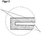
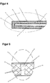
- Numeral reference in figures is as follows: 1- display portion, 2- gap portion, 3- graphic laser etching traces, 4- gap portion laser etching traces, 5- ITO segments, 6- gap, 7- cross point.
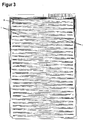
- FIG.3-5 A method for etching an indium tin oxide film on a gap portion of a capacitive touchscreen panel of the invention is shown in Fig.3-5 .
- the insulating transparent substrate has an indium tin oxide (ITO) film arranged thereon, and comprises a display portion 1 and a gap portion 2, as shown in Fig.3 , the display portion 1 and the gap portion 2 are arranged in alternating manner; under the limitation of the requirements of a control chip of the capacitive touchscreen panel, the width of the gap portion 2 is usually 0.2mm-0.3mm, the width of the gap portion 2 in the present embodiment is preferably 0.3mm.
- ITO indium tin oxide
- a laser etching line is used to cut ITO on the gap portion 2 into a plurality of ITO segments 5.
- the ITO segments are independent from and unconnected to each other; in other words, a gap 6 is formed between the adjacent ITO segments 5, and the length of the gap 6 is not specifically defined herein, as long as the adjacent ITO segments can be separated.
- Each ITO segment has a small parasitic capacitance which will almost not affect the recognition accuracy of a touch signal.
- the length of each ITO segment 5 is 2mm-4mm, in the present embodiment, the length of each ITO segment 5 is preferably 3mm.
- the method for etching uses two laser etching lines to perform cross cutting to form a plurality of the ITO segments 5 that are independent from and unconnected to each other, and two laser etching lines form gap portion laser etching traces 4 on the gap portion 2.
- the distance between centerlines of the two laser etching lines is less than the width of one laser etching line in the process of approaching the cross point of the laser etching lines.
- the distance between the centerline of the gap portion laser etching traces 4 and the centerline of graphic laser etching traces 3 of the display portion 1 of capacitive touch-screen panel is also less than the width of one laser etching line.
- the two laser etching lines run parallel to each other and partially overlap at a position close to cross point 7, and the two laser etching lines are dislocated by 0.01mm.
- the gap 6 between the adjacent ITO segments 5 forms gap portion ITO segments at a position close to the ITO segments 5 on two sides, the gap portion ITO segments are independent from and unconnected to each other, which are similar to ITO segments 5.
- the length of each ITO segment also can be 2mm, 2.5mm, 3.8m, or 4mm etc., which is chosen according to products performance requirements.
- the width of the gap portion 2 also can be 0.2mm, 0.23mm, 0.25mm, or 0.28mm etc.
Landscapes
- Engineering & Computer Science (AREA)
- Physics & Mathematics (AREA)
- Theoretical Computer Science (AREA)
- General Engineering & Computer Science (AREA)
- Optics & Photonics (AREA)
- General Physics & Mathematics (AREA)
- Human Computer Interaction (AREA)
- Plasma & Fusion (AREA)
- Mechanical Engineering (AREA)
- Quality & Reliability (AREA)
- Position Input By Displaying (AREA)
- Manufacture Of Switches (AREA)
- Devices For Indicating Variable Information By Combining Individual Elements (AREA)
Claims (9)
- Verfahren zum Ätzen einer Indium-Zinn-Oxidfolie auf einem kapazitiven Berührbildschirm, wobei die Indium-Zinn-Oxidfolie auf einem isolierenden transparenten Substrat des kapazitiven Berührbildschirms angeordnet ist, wobei die Indium-Zinn-Oxidfolie einen Spaltabschnitt (2) aufweist, der von einem ersten Satz von Laserätzspuren (3) begrenzt wird, wobei der Spaltabschnitt (2) eine Zickzackform aufweist, dadurch gekennzeichnet, dass das Verfahren umfasst:
Verwenden von Laserätzen, um einen zweiten Satz von Laserätzspuren (4) zu bilden und den Spaltabschnitt (2) in eine Vielzahl von Segmenten (5), die durch eine Vielzahl von Querspalten (6) getrennt sind, zu trennen, die voneinander unabhängig sind und nicht miteinander verbunden sind, wobei die Laserätzspuren (4) von dem zweiten Satz von Laserätzspuren (4) durch Laserätzen entlang zweier Linien gebildet werden, die beide durch die Vielzahl von Querspalten (6) verlaufen und einander an der Vielzahl von Querspalten (6) kreuzen. - Verfahren zum Ätzen nach Anspruch 1, dadurch gekennzeichnet, dass an jedem der Querspalten (6) die Mittellinien der beiden Laserätzspuren (4) von dem zweiten Satz von Laserätzspuren (4) einen Abstand von dem zweiten Satz von Laserätzspuren (4) von weniger als der Breite von einer Laserätzspur (4) haben.
- Verfahren zum Ätzen nach Anspruch 1, dadurch gekennzeichnet, dass an jeder der Querspalten (6) die beiden Laserätzspuren (4) von dem zweiten Satz von Laserätzspuren (4) parallel zueinander sind und teilweise überlappen.
- Verfahren zum Ätzen nach Anspruch 1, dadurch gekennzeichnet, dass an jedem der Querspalten (6) die Mittellinien der beiden Laserätzspuren (4) von dem zweiten Satz von Laserätzspuren (4) einen Abstand von dem zweiten Satz von Laserätzspuren (4) haben, der größer als die Breite von einer Laserätzspur (4) ist, und ein Zwischensegment zwischen benachbarten der Segmente (5) gebildet wird, wobei das Zwischensegment unabhängig von den benachbarten Segmenten (5) ist und nicht mit diesen verbunden ist.
- Verfahren zum Ätzen nach einem der Ansprüche 1 bis 3, dadurch gekennzeichnet, dass die Länge von jedem Segment (5) 2 mm bis 4 mm beträgt.
- Verfahren zum Ätzen nach Anspruch 5, dadurch gekennzeichnet, dass die Länge von jedem Segment (5) 3 mm beträgt.
- Verfahren zum Ätzen nach Anspruch 1, dadurch gekennzeichnet, dass entlang der Ätzspuren (3) von dem ersten Satz von Laserätzspuren (3) der Abstand zwischen der Mittellinie von jeder Ätzspur (3) von dem ersten Satz von Laserätzspuren (3) und der Mittellinie einer benachbarten Laserätzspur (4) des zweiten Satzes von Laserätzspuren (4) weniger als die Breite von einer Laserätzspur beträgt.
- Verfahren zum Ätzen nach Anspruch 7, dadurch gekennzeichnet, dass die Breite des Spaltabschnitts (2) 0,2 mm bis 0,3 mm beträgt.
- Kapazitiver Berührbildschirm, aufweisend eine Sensierschaltungsschicht, eine Ansteuerschaltungsschicht und ein isolierendes transparentes Substrat mit einer darauf angeordneten Indium-Zinn-Oxidfolie, wobei die Indium-Zinn-Oxidfolie einen Spaltabschnitt (2) aufweist, der von einem ersten Satz von Laserätzspuren (3) begrenzt wird, wobei der Spaltabschnitt (2) eine Zickzackform aufweist, dadurch gekennzeichnet, dass die Indium-Zinn-Oxidfolie des Spaltabschnitt (2) in eine Vielzahl von Segmenten (5) durch das Verfahren nach einem der Ansprüche 1 bis 8 getrennt wird.
Applications Claiming Priority (2)
| Application Number | Priority Date | Filing Date | Title |
|---|---|---|---|
| CN201310722462.XA CN104731422B (zh) | 2013-12-24 | 2013-12-24 | 电容屏触控面板及其间隙部分氧化铟锡薄膜的刻蚀方法 |
| PCT/CN2014/094621 WO2015096691A1 (zh) | 2013-12-24 | 2014-12-23 | 电容屏触控面板及其间隙部分氧化铟锡薄膜的刻蚀方法 |
Publications (3)
| Publication Number | Publication Date |
|---|---|
| EP3089007A1 EP3089007A1 (de) | 2016-11-02 |
| EP3089007A4 EP3089007A4 (de) | 2016-12-14 |
| EP3089007B1 true EP3089007B1 (de) | 2020-01-08 |
Family
ID=53455382
Family Applications (1)
| Application Number | Title | Priority Date | Filing Date |
|---|---|---|---|
| EP14874941.9A Active EP3089007B1 (de) | 2013-12-24 | 2014-12-23 | Verfahren zum ätzen einer indium-zinn-oxidfolie auf einem kapazitiven berührungsbildschirm |
Country Status (7)
| Country | Link |
|---|---|
| US (1) | US10379667B2 (de) |
| EP (1) | EP3089007B1 (de) |
| JP (1) | JP6300937B2 (de) |
| KR (1) | KR101908974B1 (de) |
| CN (1) | CN104731422B (de) |
| TW (1) | TWI553525B (de) |
| WO (1) | WO2015096691A1 (de) |
Families Citing this family (3)
| Publication number | Priority date | Publication date | Assignee | Title |
|---|---|---|---|---|
| CN107066157A (zh) * | 2017-03-10 | 2017-08-18 | 深圳唯科技股份有限公司 | 大尺寸电容式触摸屏及其柔性生产工艺 |
| EP3748461A4 (de) * | 2019-04-10 | 2021-03-10 | Shenzhen Goodix Technology Co., Ltd. | Herstellungsverfahren für eine leitung bei einem berührungsbildschirm, berührungsbildschirm und elektronische vorrichtung |
| CN111625153B (zh) * | 2020-05-09 | 2022-12-20 | 芜湖伦丰电子科技有限公司 | 一种触控装置及其改善双线激光拼接位良率方法 |
Citations (1)
| Publication number | Priority date | Publication date | Assignee | Title |
|---|---|---|---|---|
| US4999462A (en) * | 1989-10-06 | 1991-03-12 | Summagraphics Corporation | Position determining and digitizing method and device |
Family Cites Families (21)
| Publication number | Priority date | Publication date | Assignee | Title |
|---|---|---|---|---|
| JPH01245993A (ja) * | 1988-03-27 | 1989-10-02 | Semiconductor Energy Lab Co Ltd | 薄膜加工装置 |
| US6300594B1 (en) * | 1998-02-19 | 2001-10-09 | Ricoh Microelectronics Company, Ltd. | Method and apparatus for machining an electrically conductive film |
| CA2742985A1 (en) | 2008-11-06 | 2010-05-14 | Uico, Inc. | Capacitive touch screen and strategic geometry isolation patterning method for making touch screens |
| GB2472613B (en) * | 2009-08-11 | 2015-06-03 | M Solv Ltd | Capacitive touch panels |
| TWI392774B (zh) | 2009-09-17 | 2013-04-11 | 國立臺灣大學 | 維持材料表面平整度的製作方法 |
| US8674249B2 (en) * | 2010-08-20 | 2014-03-18 | Young Fast Optoelectronics Co., Ltd. | Capacitive touch pad |
| CN201788497U (zh) * | 2010-09-10 | 2011-04-06 | 洋华光电股份有限公司 | 电容式触控感应器结构 |
| CN102314272B (zh) * | 2010-10-26 | 2015-02-04 | 敦泰科技(深圳)有限公司 | 一种双层结构电容式触摸屏 |
| TW201229616A (en) * | 2011-01-07 | 2012-07-16 | Unidisplay Inc | Touch panel |
| JP3167700U (ja) * | 2011-02-22 | 2011-05-12 | 洋華光電股▲ふん▼有限公司 | 透明タッチコントロールセンサー |
| KR101550481B1 (ko) * | 2011-03-30 | 2015-09-04 | 주식회사 엘지화학 | 패턴 시인성이 개선된 터치 패널, 그 제조 방법 및 이를 포함하는 디스플레이 장치 |
| EP2538313B1 (de) * | 2011-06-20 | 2015-05-20 | Melfas, Inc. | Berührungssensortafel |
| TW201310472A (zh) * | 2011-08-31 | 2013-03-01 | Shih Hua Technology Ltd | 透明導電膜以及使用該透明導電膜的觸控面板 |
| CN103105962B (zh) * | 2011-11-09 | 2016-04-06 | 宸鸿科技(厦门)有限公司 | 触控面板、触控电极结构及其制作方法 |
| CN103176643A (zh) * | 2011-12-26 | 2013-06-26 | 瀚宇彩晶股份有限公司 | 触控装置及其制造方法 |
| US9312855B2 (en) * | 2012-01-10 | 2016-04-12 | Atmel Corporation | Touch sensor tracks |
| JP5812895B2 (ja) | 2012-02-28 | 2015-11-17 | 株式会社ジャパンディスプレイ | 近接検出装置、近接検出方法、電子機器 |
| JP2013254246A (ja) | 2012-06-05 | 2013-12-19 | Nissha Printing Co Ltd | 導電性ナノファイバーシート及びこれを用いたタッチパネル |
| CN202854790U (zh) * | 2012-11-09 | 2013-04-03 | 张汝箱 | 电容式触摸屏 |
| US20140267073A1 (en) * | 2013-03-14 | 2014-09-18 | Teco Nanotech Co., Ltd. | Touch panel structural and display device using touch panel |
| US9282645B2 (en) * | 2013-12-16 | 2016-03-08 | Industrial Technology Research Institute | Laser patterning of frame wire area on touch panel |
-
2013
- 2013-12-24 CN CN201310722462.XA patent/CN104731422B/zh active Active
-
2014
- 2014-12-23 EP EP14874941.9A patent/EP3089007B1/de active Active
- 2014-12-23 JP JP2016543157A patent/JP6300937B2/ja active Active
- 2014-12-23 US US15/107,301 patent/US10379667B2/en active Active
- 2014-12-23 KR KR1020167018590A patent/KR101908974B1/ko active Active
- 2014-12-23 WO PCT/CN2014/094621 patent/WO2015096691A1/zh not_active Ceased
- 2014-12-24 TW TW103145332A patent/TWI553525B/zh active
Patent Citations (1)
| Publication number | Priority date | Publication date | Assignee | Title |
|---|---|---|---|---|
| US4999462A (en) * | 1989-10-06 | 1991-03-12 | Summagraphics Corporation | Position determining and digitizing method and device |
Also Published As
| Publication number | Publication date |
|---|---|
| TWI553525B (zh) | 2016-10-11 |
| TW201525811A (zh) | 2015-07-01 |
| JP6300937B2 (ja) | 2018-03-28 |
| KR20160096185A (ko) | 2016-08-12 |
| CN104731422A (zh) | 2015-06-24 |
| JP2017501503A (ja) | 2017-01-12 |
| US10379667B2 (en) | 2019-08-13 |
| US20170003820A1 (en) | 2017-01-05 |
| KR101908974B1 (ko) | 2018-10-17 |
| CN104731422B (zh) | 2018-06-26 |
| WO2015096691A1 (zh) | 2015-07-02 |
| EP3089007A4 (de) | 2016-12-14 |
| EP3089007A1 (de) | 2016-11-02 |
Similar Documents
| Publication | Publication Date | Title |
|---|---|---|
| US9720541B2 (en) | Arrangement of sensor pads and display driver pads for input device | |
| EP2728450B1 (de) | Kapazitiver In-Zellen-Berührungsbildschirm, Ansteuerungsverfahren dafür und Anzeigevorrichtung | |
| EP2735948B1 (de) | Berührungsempfindlicher induktor, eingebettete berührungsempfindliche flüssigkristallanzeigetafel und flüssigkristallanzeige | |
| KR101330779B1 (ko) | 터치 패널의 전극 구조, 그 방법 및 터치 패널 | |
| KR101850660B1 (ko) | 전자기 용량 터치스크린 | |
| US20140347319A1 (en) | Touch panel | |
| JP6143587B2 (ja) | タッチパネル、タッチパネル付き表示装置 | |
| US9423918B2 (en) | Electrostatic capacitive touch screen panel | |
| EP2738596A1 (de) | Flüssigkristallanzeigevorrichtung mit berührungssteuerung | |
| US9291847B2 (en) | Pixel unit and TFT-LCD with touch function | |
| EP2811482A1 (de) | Berührungsflüssigkristallanzeigevorrichtung | |
| TWI588728B (zh) | 觸控面板之互容式觸控感測元件 | |
| US11269465B2 (en) | Mutual capacitive touch panel with double-layer electrodes | |
| US20160328046A1 (en) | Touch panel and display device | |
| US20150029422A1 (en) | Touch panel and touch display panel | |
| EP2784637B1 (de) | Berührungsbildschirm, Berührungsanzeigetafel und Berührungsanzeigevorrichtung | |
| US10379667B2 (en) | Capacitive touchscreen panel and a method for etching an indium tin oxide film on a gap portion of a capacitive touchscreen panel | |
| US10310691B2 (en) | Self-capacitance touch structure having touch electrodes with side wing portions and display device thereof | |
| US9652102B2 (en) | Touch panel | |
| CN207833482U (zh) | 具有双层电极结构的互容式触控面板 | |
| CN103902093B (zh) | 触摸板及触摸显示器 | |
| CN106527782A (zh) | 触控面板 | |
| JP2017227982A (ja) | 導電性パターン基板およびタッチ位置検出機能付き表示装置 | |
| TWI620108B (zh) | 觸控面板 |
Legal Events
| Date | Code | Title | Description |
|---|---|---|---|
| PUAI | Public reference made under article 153(3) epc to a published international application that has entered the european phase |
Free format text: ORIGINAL CODE: 0009012 |
|
| 17P | Request for examination filed |
Effective date: 20160623 |
|
| AK | Designated contracting states |
Kind code of ref document: A1 Designated state(s): AL AT BE BG CH CY CZ DE DK EE ES FI FR GB GR HR HU IE IS IT LI LT LU LV MC MK MT NL NO PL PT RO RS SE SI SK SM TR |
|
| AX | Request for extension of the european patent |
Extension state: BA ME |
|
| A4 | Supplementary search report drawn up and despatched |
Effective date: 20161110 |
|
| RIC1 | Information provided on ipc code assigned before grant |
Ipc: G06F 3/044 20060101AFI20161104BHEP |
|
| DAX | Request for extension of the european patent (deleted) | ||
| STAA | Information on the status of an ep patent application or granted ep patent |
Free format text: STATUS: EXAMINATION IS IN PROGRESS |
|
| 17Q | First examination report despatched |
Effective date: 20171013 |
|
| GRAP | Despatch of communication of intention to grant a patent |
Free format text: ORIGINAL CODE: EPIDOSNIGR1 |
|
| STAA | Information on the status of an ep patent application or granted ep patent |
Free format text: STATUS: GRANT OF PATENT IS INTENDED |
|
| INTG | Intention to grant announced |
Effective date: 20191017 |
|
| GRAS | Grant fee paid |
Free format text: ORIGINAL CODE: EPIDOSNIGR3 |
|
| GRAA | (expected) grant |
Free format text: ORIGINAL CODE: 0009210 |
|
| STAA | Information on the status of an ep patent application or granted ep patent |
Free format text: STATUS: THE PATENT HAS BEEN GRANTED |
|
| AK | Designated contracting states |
Kind code of ref document: B1 Designated state(s): AL AT BE BG CH CY CZ DE DK EE ES FI FR GB GR HR HU IE IS IT LI LT LU LV MC MK MT NL NO PL PT RO RS SE SI SK SM TR |
|
| REG | Reference to a national code |
Ref country code: GB Ref legal event code: FG4D |
|
| REG | Reference to a national code |
Ref country code: CH Ref legal event code: EP |
|
| REG | Reference to a national code |
Ref country code: DE Ref legal event code: R096 Ref document number: 602014059899 Country of ref document: DE |
|
| REG | Reference to a national code |
Ref country code: IE Ref legal event code: FG4D |
|
| REG | Reference to a national code |
Ref country code: AT Ref legal event code: REF Ref document number: 1223506 Country of ref document: AT Kind code of ref document: T Effective date: 20200215 |
|
| REG | Reference to a national code |
Ref country code: NL Ref legal event code: MP Effective date: 20200108 |
|
| REG | Reference to a national code |
Ref country code: LT Ref legal event code: MG4D |
|
| PG25 | Lapsed in a contracting state [announced via postgrant information from national office to epo] |
Ref country code: LT Free format text: LAPSE BECAUSE OF FAILURE TO SUBMIT A TRANSLATION OF THE DESCRIPTION OR TO PAY THE FEE WITHIN THE PRESCRIBED TIME-LIMIT Effective date: 20200108 Ref country code: NL Free format text: LAPSE BECAUSE OF FAILURE TO SUBMIT A TRANSLATION OF THE DESCRIPTION OR TO PAY THE FEE WITHIN THE PRESCRIBED TIME-LIMIT Effective date: 20200108 Ref country code: NO Free format text: LAPSE BECAUSE OF FAILURE TO SUBMIT A TRANSLATION OF THE DESCRIPTION OR TO PAY THE FEE WITHIN THE PRESCRIBED TIME-LIMIT Effective date: 20200408 Ref country code: FI Free format text: LAPSE BECAUSE OF FAILURE TO SUBMIT A TRANSLATION OF THE DESCRIPTION OR TO PAY THE FEE WITHIN THE PRESCRIBED TIME-LIMIT Effective date: 20200108 Ref country code: RS Free format text: LAPSE BECAUSE OF FAILURE TO SUBMIT A TRANSLATION OF THE DESCRIPTION OR TO PAY THE FEE WITHIN THE PRESCRIBED TIME-LIMIT Effective date: 20200108 Ref country code: PT Free format text: LAPSE BECAUSE OF FAILURE TO SUBMIT A TRANSLATION OF THE DESCRIPTION OR TO PAY THE FEE WITHIN THE PRESCRIBED TIME-LIMIT Effective date: 20200531 |
|
| PG25 | Lapsed in a contracting state [announced via postgrant information from national office to epo] |
Ref country code: GR Free format text: LAPSE BECAUSE OF FAILURE TO SUBMIT A TRANSLATION OF THE DESCRIPTION OR TO PAY THE FEE WITHIN THE PRESCRIBED TIME-LIMIT Effective date: 20200409 Ref country code: HR Free format text: LAPSE BECAUSE OF FAILURE TO SUBMIT A TRANSLATION OF THE DESCRIPTION OR TO PAY THE FEE WITHIN THE PRESCRIBED TIME-LIMIT Effective date: 20200108 Ref country code: BG Free format text: LAPSE BECAUSE OF FAILURE TO SUBMIT A TRANSLATION OF THE DESCRIPTION OR TO PAY THE FEE WITHIN THE PRESCRIBED TIME-LIMIT Effective date: 20200408 Ref country code: SE Free format text: LAPSE BECAUSE OF FAILURE TO SUBMIT A TRANSLATION OF THE DESCRIPTION OR TO PAY THE FEE WITHIN THE PRESCRIBED TIME-LIMIT Effective date: 20200108 Ref country code: LV Free format text: LAPSE BECAUSE OF FAILURE TO SUBMIT A TRANSLATION OF THE DESCRIPTION OR TO PAY THE FEE WITHIN THE PRESCRIBED TIME-LIMIT Effective date: 20200108 Ref country code: IS Free format text: LAPSE BECAUSE OF FAILURE TO SUBMIT A TRANSLATION OF THE DESCRIPTION OR TO PAY THE FEE WITHIN THE PRESCRIBED TIME-LIMIT Effective date: 20200508 |
|
| REG | Reference to a national code |
Ref country code: DE Ref legal event code: R097 Ref document number: 602014059899 Country of ref document: DE |
|
| PG25 | Lapsed in a contracting state [announced via postgrant information from national office to epo] |
Ref country code: RO Free format text: LAPSE BECAUSE OF FAILURE TO SUBMIT A TRANSLATION OF THE DESCRIPTION OR TO PAY THE FEE WITHIN THE PRESCRIBED TIME-LIMIT Effective date: 20200108 Ref country code: ES Free format text: LAPSE BECAUSE OF FAILURE TO SUBMIT A TRANSLATION OF THE DESCRIPTION OR TO PAY THE FEE WITHIN THE PRESCRIBED TIME-LIMIT Effective date: 20200108 Ref country code: CZ Free format text: LAPSE BECAUSE OF FAILURE TO SUBMIT A TRANSLATION OF THE DESCRIPTION OR TO PAY THE FEE WITHIN THE PRESCRIBED TIME-LIMIT Effective date: 20200108 Ref country code: SK Free format text: LAPSE BECAUSE OF FAILURE TO SUBMIT A TRANSLATION OF THE DESCRIPTION OR TO PAY THE FEE WITHIN THE PRESCRIBED TIME-LIMIT Effective date: 20200108 Ref country code: DK Free format text: LAPSE BECAUSE OF FAILURE TO SUBMIT A TRANSLATION OF THE DESCRIPTION OR TO PAY THE FEE WITHIN THE PRESCRIBED TIME-LIMIT Effective date: 20200108 Ref country code: SM Free format text: LAPSE BECAUSE OF FAILURE TO SUBMIT A TRANSLATION OF THE DESCRIPTION OR TO PAY THE FEE WITHIN THE PRESCRIBED TIME-LIMIT Effective date: 20200108 Ref country code: EE Free format text: LAPSE BECAUSE OF FAILURE TO SUBMIT A TRANSLATION OF THE DESCRIPTION OR TO PAY THE FEE WITHIN THE PRESCRIBED TIME-LIMIT Effective date: 20200108 |
|
| PLBE | No opposition filed within time limit |
Free format text: ORIGINAL CODE: 0009261 |
|
| STAA | Information on the status of an ep patent application or granted ep patent |
Free format text: STATUS: NO OPPOSITION FILED WITHIN TIME LIMIT |
|
| REG | Reference to a national code |
Ref country code: AT Ref legal event code: MK05 Ref document number: 1223506 Country of ref document: AT Kind code of ref document: T Effective date: 20200108 |
|
| 26N | No opposition filed |
Effective date: 20201009 |
|
| PG25 | Lapsed in a contracting state [announced via postgrant information from national office to epo] |
Ref country code: AT Free format text: LAPSE BECAUSE OF FAILURE TO SUBMIT A TRANSLATION OF THE DESCRIPTION OR TO PAY THE FEE WITHIN THE PRESCRIBED TIME-LIMIT Effective date: 20200108 Ref country code: IT Free format text: LAPSE BECAUSE OF FAILURE TO SUBMIT A TRANSLATION OF THE DESCRIPTION OR TO PAY THE FEE WITHIN THE PRESCRIBED TIME-LIMIT Effective date: 20200108 |
|
| PG25 | Lapsed in a contracting state [announced via postgrant information from national office to epo] |
Ref country code: PL Free format text: LAPSE BECAUSE OF FAILURE TO SUBMIT A TRANSLATION OF THE DESCRIPTION OR TO PAY THE FEE WITHIN THE PRESCRIBED TIME-LIMIT Effective date: 20200108 Ref country code: SI Free format text: LAPSE BECAUSE OF FAILURE TO SUBMIT A TRANSLATION OF THE DESCRIPTION OR TO PAY THE FEE WITHIN THE PRESCRIBED TIME-LIMIT Effective date: 20200108 |
|
| REG | Reference to a national code |
Ref country code: CH Ref legal event code: PL |
|
| PG25 | Lapsed in a contracting state [announced via postgrant information from national office to epo] |
Ref country code: MC Free format text: LAPSE BECAUSE OF FAILURE TO SUBMIT A TRANSLATION OF THE DESCRIPTION OR TO PAY THE FEE WITHIN THE PRESCRIBED TIME-LIMIT Effective date: 20200108 |
|
| REG | Reference to a national code |
Ref country code: BE Ref legal event code: MM Effective date: 20201231 |
|
| PG25 | Lapsed in a contracting state [announced via postgrant information from national office to epo] |
Ref country code: LU Free format text: LAPSE BECAUSE OF NON-PAYMENT OF DUE FEES Effective date: 20201223 Ref country code: IE Free format text: LAPSE BECAUSE OF NON-PAYMENT OF DUE FEES Effective date: 20201223 |
|
| PG25 | Lapsed in a contracting state [announced via postgrant information from national office to epo] |
Ref country code: CH Free format text: LAPSE BECAUSE OF NON-PAYMENT OF DUE FEES Effective date: 20201231 Ref country code: LI Free format text: LAPSE BECAUSE OF NON-PAYMENT OF DUE FEES Effective date: 20201231 |
|
| PG25 | Lapsed in a contracting state [announced via postgrant information from national office to epo] |
Ref country code: TR Free format text: LAPSE BECAUSE OF FAILURE TO SUBMIT A TRANSLATION OF THE DESCRIPTION OR TO PAY THE FEE WITHIN THE PRESCRIBED TIME-LIMIT Effective date: 20200108 Ref country code: MT Free format text: LAPSE BECAUSE OF FAILURE TO SUBMIT A TRANSLATION OF THE DESCRIPTION OR TO PAY THE FEE WITHIN THE PRESCRIBED TIME-LIMIT Effective date: 20200108 Ref country code: CY Free format text: LAPSE BECAUSE OF FAILURE TO SUBMIT A TRANSLATION OF THE DESCRIPTION OR TO PAY THE FEE WITHIN THE PRESCRIBED TIME-LIMIT Effective date: 20200108 |
|
| PG25 | Lapsed in a contracting state [announced via postgrant information from national office to epo] |
Ref country code: MK Free format text: LAPSE BECAUSE OF FAILURE TO SUBMIT A TRANSLATION OF THE DESCRIPTION OR TO PAY THE FEE WITHIN THE PRESCRIBED TIME-LIMIT Effective date: 20200108 Ref country code: AL Free format text: LAPSE BECAUSE OF FAILURE TO SUBMIT A TRANSLATION OF THE DESCRIPTION OR TO PAY THE FEE WITHIN THE PRESCRIBED TIME-LIMIT Effective date: 20200108 |
|
| PG25 | Lapsed in a contracting state [announced via postgrant information from national office to epo] |
Ref country code: BE Free format text: LAPSE BECAUSE OF NON-PAYMENT OF DUE FEES Effective date: 20201231 |
|
| P01 | Opt-out of the competence of the unified patent court (upc) registered |
Effective date: 20230526 |
|
| PGFP | Annual fee paid to national office [announced via postgrant information from national office to epo] |
Ref country code: GB Payment date: 20251229 Year of fee payment: 12 |
|
| PGFP | Annual fee paid to national office [announced via postgrant information from national office to epo] |
Ref country code: FR Payment date: 20251230 Year of fee payment: 12 |
|
| PGFP | Annual fee paid to national office [announced via postgrant information from national office to epo] |
Ref country code: DE Payment date: 20251231 Year of fee payment: 12 |