EP3082152B1 - Einschichtfilme aus halbleitenden metalldichalcogeniden, verfahren zur herstellung davon und verwendungen davon - Google Patents
Einschichtfilme aus halbleitenden metalldichalcogeniden, verfahren zur herstellung davon und verwendungen davon Download PDFInfo
- Publication number
- EP3082152B1 EP3082152B1 EP16165628.5A EP16165628A EP3082152B1 EP 3082152 B1 EP3082152 B1 EP 3082152B1 EP 16165628 A EP16165628 A EP 16165628A EP 3082152 B1 EP3082152 B1 EP 3082152B1
- Authority
- EP
- European Patent Office
- Prior art keywords
- mos
- film
- growth
- films
- chalcogenide
- Prior art date
- Legal status (The legal status is an assumption and is not a legal conclusion. Google has not performed a legal analysis and makes no representation as to the accuracy of the status listed.)
- Active
Links
Images








Classifications
-
- H—ELECTRICITY
- H10—SEMICONDUCTOR DEVICES; ELECTRIC SOLID-STATE DEVICES NOT OTHERWISE PROVIDED FOR
- H10P—GENERIC PROCESSES OR APPARATUS FOR THE MANUFACTURE OR TREATMENT OF DEVICES COVERED BY CLASS H10
- H10P14/00—Formation of materials, e.g. in the shape of layers or pillars
- H10P14/20—Formation of materials, e.g. in the shape of layers or pillars of semiconductor materials
- H10P14/32—Formation of materials, e.g. in the shape of layers or pillars of semiconductor materials characterised by intermediate layers between substrates and deposited layers
- H10P14/3202—Materials thereof
- H10P14/3236—Materials thereof being chalcogenide semiconducting materials not being oxides, e.g. ternary compounds
-
- C—CHEMISTRY; METALLURGY
- C23—COATING METALLIC MATERIAL; COATING MATERIAL WITH METALLIC MATERIAL; CHEMICAL SURFACE TREATMENT; DIFFUSION TREATMENT OF METALLIC MATERIAL; COATING BY VACUUM EVAPORATION, BY SPUTTERING, BY ION IMPLANTATION OR BY CHEMICAL VAPOUR DEPOSITION, IN GENERAL; INHIBITING CORROSION OF METALLIC MATERIAL OR INCRUSTATION IN GENERAL
- C23C—COATING METALLIC MATERIAL; COATING MATERIAL WITH METALLIC MATERIAL; SURFACE TREATMENT OF METALLIC MATERIAL BY DIFFUSION INTO THE SURFACE, BY CHEMICAL CONVERSION OR SUBSTITUTION; COATING BY VACUUM EVAPORATION, BY SPUTTERING, BY ION IMPLANTATION OR BY CHEMICAL VAPOUR DEPOSITION, IN GENERAL
- C23C16/00—Chemical coating by decomposition of gaseous compounds, without leaving reaction products of surface material in the coating, i.e. chemical vapour deposition [CVD] processes
- C23C16/22—Chemical coating by decomposition of gaseous compounds, without leaving reaction products of surface material in the coating, i.e. chemical vapour deposition [CVD] processes characterised by the deposition of inorganic material, other than metallic material
- C23C16/30—Deposition of compounds, mixtures or solid solutions, e.g. borides, carbides, nitrides
- C23C16/305—Sulfides, selenides, or tellurides
-
- H—ELECTRICITY
- H10—SEMICONDUCTOR DEVICES; ELECTRIC SOLID-STATE DEVICES NOT OTHERWISE PROVIDED FOR
- H10D—INORGANIC ELECTRIC SEMICONDUCTOR DEVICES
- H10D62/00—Semiconductor bodies, or regions thereof, of devices having potential barriers
- H10D62/80—Semiconductor bodies, or regions thereof, of devices having potential barriers characterised by the materials
-
- C—CHEMISTRY; METALLURGY
- C23—COATING METALLIC MATERIAL; COATING MATERIAL WITH METALLIC MATERIAL; CHEMICAL SURFACE TREATMENT; DIFFUSION TREATMENT OF METALLIC MATERIAL; COATING BY VACUUM EVAPORATION, BY SPUTTERING, BY ION IMPLANTATION OR BY CHEMICAL VAPOUR DEPOSITION, IN GENERAL; INHIBITING CORROSION OF METALLIC MATERIAL OR INCRUSTATION IN GENERAL
- C23C—COATING METALLIC MATERIAL; COATING MATERIAL WITH METALLIC MATERIAL; SURFACE TREATMENT OF METALLIC MATERIAL BY DIFFUSION INTO THE SURFACE, BY CHEMICAL CONVERSION OR SUBSTITUTION; COATING BY VACUUM EVAPORATION, BY SPUTTERING, BY ION IMPLANTATION OR BY CHEMICAL VAPOUR DEPOSITION, IN GENERAL
- C23C16/00—Chemical coating by decomposition of gaseous compounds, without leaving reaction products of surface material in the coating, i.e. chemical vapour deposition [CVD] processes
- C23C16/44—Chemical coating by decomposition of gaseous compounds, without leaving reaction products of surface material in the coating, i.e. chemical vapour deposition [CVD] processes characterised by the method of coating
- C23C16/52—Controlling or regulating the coating process
-
- C—CHEMISTRY; METALLURGY
- C30—CRYSTAL GROWTH
- C30B—SINGLE-CRYSTAL GROWTH; UNIDIRECTIONAL SOLIDIFICATION OF EUTECTIC MATERIAL OR UNIDIRECTIONAL DEMIXING OF EUTECTOID MATERIAL; REFINING BY ZONE-MELTING OF MATERIAL; PRODUCTION OF A HOMOGENEOUS POLYCRYSTALLINE MATERIAL WITH DEFINED STRUCTURE; SINGLE CRYSTALS OR HOMOGENEOUS POLYCRYSTALLINE MATERIAL WITH DEFINED STRUCTURE; AFTER-TREATMENT OF SINGLE CRYSTALS OR A HOMOGENEOUS POLYCRYSTALLINE MATERIAL WITH DEFINED STRUCTURE; APPARATUS THEREFOR
- C30B25/00—Single-crystal growth by chemical reaction of reactive gases, e.g. chemical vapour-deposition growth
-
- C—CHEMISTRY; METALLURGY
- C30—CRYSTAL GROWTH
- C30B—SINGLE-CRYSTAL GROWTH; UNIDIRECTIONAL SOLIDIFICATION OF EUTECTIC MATERIAL OR UNIDIRECTIONAL DEMIXING OF EUTECTOID MATERIAL; REFINING BY ZONE-MELTING OF MATERIAL; PRODUCTION OF A HOMOGENEOUS POLYCRYSTALLINE MATERIAL WITH DEFINED STRUCTURE; SINGLE CRYSTALS OR HOMOGENEOUS POLYCRYSTALLINE MATERIAL WITH DEFINED STRUCTURE; AFTER-TREATMENT OF SINGLE CRYSTALS OR A HOMOGENEOUS POLYCRYSTALLINE MATERIAL WITH DEFINED STRUCTURE; APPARATUS THEREFOR
- C30B29/00—Single crystals or homogeneous polycrystalline material with defined structure characterised by the material or by their shape
- C30B29/10—Inorganic compounds or compositions
- C30B29/46—Sulfur-, selenium- or tellurium-containing compounds
-
- H—ELECTRICITY
- H10—SEMICONDUCTOR DEVICES; ELECTRIC SOLID-STATE DEVICES NOT OTHERWISE PROVIDED FOR
- H10D—INORGANIC ELECTRIC SEMICONDUCTOR DEVICES
- H10D30/00—Field-effect transistors [FET]
- H10D30/60—Insulated-gate field-effect transistors [IGFET]
- H10D30/67—Thin-film transistors [TFT]
-
- H—ELECTRICITY
- H10—SEMICONDUCTOR DEVICES; ELECTRIC SOLID-STATE DEVICES NOT OTHERWISE PROVIDED FOR
- H10D—INORGANIC ELECTRIC SEMICONDUCTOR DEVICES
- H10D62/00—Semiconductor bodies, or regions thereof, of devices having potential barriers
- H10D62/80—Semiconductor bodies, or regions thereof, of devices having potential barriers characterised by the materials
- H10D62/881—Semiconductor bodies, or regions thereof, of devices having potential barriers characterised by the materials being a two-dimensional material
- H10D62/883—Transition metal dichalcogenides, e.g. MoSe2
-
- H—ELECTRICITY
- H10—SEMICONDUCTOR DEVICES; ELECTRIC SOLID-STATE DEVICES NOT OTHERWISE PROVIDED FOR
- H10D—INORGANIC ELECTRIC SEMICONDUCTOR DEVICES
- H10D99/00—Subject matter not provided for in other groups of this subclass
-
- H—ELECTRICITY
- H10—SEMICONDUCTOR DEVICES; ELECTRIC SOLID-STATE DEVICES NOT OTHERWISE PROVIDED FOR
- H10P—GENERIC PROCESSES OR APPARATUS FOR THE MANUFACTURE OR TREATMENT OF DEVICES COVERED BY CLASS H10
- H10P14/00—Formation of materials, e.g. in the shape of layers or pillars
- H10P14/20—Formation of materials, e.g. in the shape of layers or pillars of semiconductor materials
- H10P14/24—Formation of materials, e.g. in the shape of layers or pillars of semiconductor materials using chemical vapour deposition [CVD]
-
- H—ELECTRICITY
- H10—SEMICONDUCTOR DEVICES; ELECTRIC SOLID-STATE DEVICES NOT OTHERWISE PROVIDED FOR
- H10P—GENERIC PROCESSES OR APPARATUS FOR THE MANUFACTURE OR TREATMENT OF DEVICES COVERED BY CLASS H10
- H10P14/00—Formation of materials, e.g. in the shape of layers or pillars
- H10P14/20—Formation of materials, e.g. in the shape of layers or pillars of semiconductor materials
- H10P14/29—Formation of materials, e.g. in the shape of layers or pillars of semiconductor materials characterised by the substrates
- H10P14/2901—Materials
- H10P14/2902—Materials being Group IVA materials
- H10P14/2905—Silicon, silicon germanium or germanium
-
- H—ELECTRICITY
- H10—SEMICONDUCTOR DEVICES; ELECTRIC SOLID-STATE DEVICES NOT OTHERWISE PROVIDED FOR
- H10P—GENERIC PROCESSES OR APPARATUS FOR THE MANUFACTURE OR TREATMENT OF DEVICES COVERED BY CLASS H10
- H10P14/00—Formation of materials, e.g. in the shape of layers or pillars
- H10P14/20—Formation of materials, e.g. in the shape of layers or pillars of semiconductor materials
- H10P14/29—Formation of materials, e.g. in the shape of layers or pillars of semiconductor materials characterised by the substrates
- H10P14/2901—Materials
- H10P14/2919—Materials being chalcogenide semiconducting materials not being oxides, e.g. ternary compounds
-
- H—ELECTRICITY
- H10—SEMICONDUCTOR DEVICES; ELECTRIC SOLID-STATE DEVICES NOT OTHERWISE PROVIDED FOR
- H10P—GENERIC PROCESSES OR APPARATUS FOR THE MANUFACTURE OR TREATMENT OF DEVICES COVERED BY CLASS H10
- H10P14/00—Formation of materials, e.g. in the shape of layers or pillars
- H10P14/20—Formation of materials, e.g. in the shape of layers or pillars of semiconductor materials
- H10P14/29—Formation of materials, e.g. in the shape of layers or pillars of semiconductor materials characterised by the substrates
- H10P14/2901—Materials
- H10P14/2921—Materials being crystalline insulating materials
-
- H—ELECTRICITY
- H10—SEMICONDUCTOR DEVICES; ELECTRIC SOLID-STATE DEVICES NOT OTHERWISE PROVIDED FOR
- H10P—GENERIC PROCESSES OR APPARATUS FOR THE MANUFACTURE OR TREATMENT OF DEVICES COVERED BY CLASS H10
- H10P14/00—Formation of materials, e.g. in the shape of layers or pillars
- H10P14/20—Formation of materials, e.g. in the shape of layers or pillars of semiconductor materials
- H10P14/29—Formation of materials, e.g. in the shape of layers or pillars of semiconductor materials characterised by the substrates
- H10P14/2901—Materials
- H10P14/2922—Materials being non-crystalline insulating materials, e.g. glass or polymers
-
- H—ELECTRICITY
- H10—SEMICONDUCTOR DEVICES; ELECTRIC SOLID-STATE DEVICES NOT OTHERWISE PROVIDED FOR
- H10P—GENERIC PROCESSES OR APPARATUS FOR THE MANUFACTURE OR TREATMENT OF DEVICES COVERED BY CLASS H10
- H10P14/00—Formation of materials, e.g. in the shape of layers or pillars
- H10P14/20—Formation of materials, e.g. in the shape of layers or pillars of semiconductor materials
- H10P14/32—Formation of materials, e.g. in the shape of layers or pillars of semiconductor materials characterised by intermediate layers between substrates and deposited layers
- H10P14/3202—Materials thereof
- H10P14/3238—Materials thereof being insulating materials
-
- H—ELECTRICITY
- H10—SEMICONDUCTOR DEVICES; ELECTRIC SOLID-STATE DEVICES NOT OTHERWISE PROVIDED FOR
- H10P—GENERIC PROCESSES OR APPARATUS FOR THE MANUFACTURE OR TREATMENT OF DEVICES COVERED BY CLASS H10
- H10P14/00—Formation of materials, e.g. in the shape of layers or pillars
- H10P14/20—Formation of materials, e.g. in the shape of layers or pillars of semiconductor materials
- H10P14/32—Formation of materials, e.g. in the shape of layers or pillars of semiconductor materials characterised by intermediate layers between substrates and deposited layers
- H10P14/3202—Materials thereof
- H10P14/3241—Materials thereof being conductive materials
-
- H—ELECTRICITY
- H10—SEMICONDUCTOR DEVICES; ELECTRIC SOLID-STATE DEVICES NOT OTHERWISE PROVIDED FOR
- H10P—GENERIC PROCESSES OR APPARATUS FOR THE MANUFACTURE OR TREATMENT OF DEVICES COVERED BY CLASS H10
- H10P14/00—Formation of materials, e.g. in the shape of layers or pillars
- H10P14/20—Formation of materials, e.g. in the shape of layers or pillars of semiconductor materials
- H10P14/32—Formation of materials, e.g. in the shape of layers or pillars of semiconductor materials characterised by intermediate layers between substrates and deposited layers
- H10P14/3242—Structure
- H10P14/3244—Layer structure
- H10P14/3246—Monolayers
-
- H—ELECTRICITY
- H10—SEMICONDUCTOR DEVICES; ELECTRIC SOLID-STATE DEVICES NOT OTHERWISE PROVIDED FOR
- H10P—GENERIC PROCESSES OR APPARATUS FOR THE MANUFACTURE OR TREATMENT OF DEVICES COVERED BY CLASS H10
- H10P14/00—Formation of materials, e.g. in the shape of layers or pillars
- H10P14/20—Formation of materials, e.g. in the shape of layers or pillars of semiconductor materials
- H10P14/34—Deposited materials, e.g. layers
- H10P14/3402—Deposited materials, e.g. layers characterised by the chemical composition
- H10P14/3436—Deposited materials, e.g. layers characterised by the chemical composition being chalcogenide semiconductor materials not being oxides, e.g. ternary compounds
-
- H—ELECTRICITY
- H10—SEMICONDUCTOR DEVICES; ELECTRIC SOLID-STATE DEVICES NOT OTHERWISE PROVIDED FOR
- H10P—GENERIC PROCESSES OR APPARATUS FOR THE MANUFACTURE OR TREATMENT OF DEVICES COVERED BY CLASS H10
- H10P14/00—Formation of materials, e.g. in the shape of layers or pillars
- H10P14/40—Formation of materials, e.g. in the shape of layers or pillars of conductive or resistive materials
- H10P14/42—Formation of materials, e.g. in the shape of layers or pillars of conductive or resistive materials using a gas or vapour
- H10P14/43—Chemical deposition, e.g. chemical vapour deposition [CVD]
-
- H—ELECTRICITY
- H10—SEMICONDUCTOR DEVICES; ELECTRIC SOLID-STATE DEVICES NOT OTHERWISE PROVIDED FOR
- H10P—GENERIC PROCESSES OR APPARATUS FOR THE MANUFACTURE OR TREATMENT OF DEVICES COVERED BY CLASS H10
- H10P14/00—Formation of materials, e.g. in the shape of layers or pillars
- H10P14/60—Formation of materials, e.g. in the shape of layers or pillars of insulating materials
- H10P14/63—Formation of materials, e.g. in the shape of layers or pillars of insulating materials characterised by the formation processes
- H10P14/6326—Deposition processes
- H10P14/6328—Deposition from the gas or vapour phase
- H10P14/6334—Deposition from the gas or vapour phase using decomposition or reaction of gaseous or vapour phase compounds, i.e. chemical vapour deposition
- H10P14/6339—Deposition from the gas or vapour phase using decomposition or reaction of gaseous or vapour phase compounds, i.e. chemical vapour deposition deposition by cyclic CVD, e.g. ALD, ALE or pulsed CVD
Definitions
- the present disclosure generally relates to a method of making metal-chalcogenide films.
- the present invention provides methods for making a metal-chalcogenide film on a substrate as defined in the appended claims.
- metal-chalcogenide films also referred to herein as metal-dichalcogenide films.
- the films can have one or more metal and/or one or more chalcogenide.
- the films comprise one or more monolayers of a metal-chalcogenide disposed on (i.e., in contact with) a substrate.
- the films exhibit desirable spatial uniformity and/or electrical performance.
- the films are crystalline.
- the films comprise 1 to 10 metal-chalcogenide monolayers.
- the present invention provides a method of making the metal-chalcogenide films.
- the methods are based on low metal precursor concentration relative to the concentration of chalcogenide precursor.
- the methods are based on a layer-by-layer growth mode.
- the films that are disclosed herein may be formed by a method of the present disclosure.
- the method for making the metal-chalcogenide films on a substrate comprises: contacting a metal precursor, a chalcogenide precursor, a reducing gas (e.g., hydrogen gas), and a substrate in a reactor such that the metal-chalcogenide film is formed on the substrate.
- a metal precursor e.g., a chalcogenide precursor, a reducing gas (e.g., hydrogen gas)
- a substrate e.g., hydrogen gas
- the precursors are present at low pressure in the reactor and in the gas phase.
- the films are not formed by sublimation of a precursor.
- a device e.g., an electronic device
- the films can be used in, for example, transistors, P-N junctions, logic circuits, analog circuits.
- devices include, but are not limited to, lasers, photo-diodes, optical modulators, piezoelectric devices, memory devices, and thin film transistor on transparent substrates.
- the films can provide a functionality of a device.
- the films can be used in transistors, P-N junctions, logic circuits, and analog circuits in devices such as, but not limit to lasers, photo-diodes, optical modulators, piezoelectric devices, memory devices, and thin film transistors.
- an optical fiber comprises one or more metal-chalcogenide film of the present disclosure.
- the optical fiber can be used in an optical modulator.
- TMDs transition metal dichalcogenides
- MLs three-atom-thick monolayers
- US 2014/027775 A1 discloses a method for forming a metal chalcogenide material, as well as related methods for forming semiconductor device structures.
- Dong Mao et al. disclose the preparation and characterization of WS 2 nanosheets.
- Hailong Zhou et al. disclose large area growth and electrical properties of p-type WSe 2 atomic layers.
- Kranthi Kumar et al. disclose the chemical vapor deposition of crystalline layers of transition metal chalcogenides such as MoS 2 .
- Sina Najmaei et al (ACS Nano, 2014, vol. 8, no. 8, pages 7930-7937 ) discloses electrical properties of polycrystalline monolayer Molybdenum Disulphide.
- the present disclosure provides metal-chalcogenide films comprising one or more monolayers of a metal-chalcogenide on a substrate. Also provided are methods of making the films and using the films. Although the present invention as defined in the appended claims relates to methods of making the films, the disclosures relating to the films and uses of the films provide technical context.
- the films are grown using a novel metal-organic chemical vapour deposition (MOCVD) technique, and show desirable electrical performance, including an electron mobility of 30 cm 2 /Vs at room temperature and 114 cm 2 /Vs at 90 K for MoS 2 , with little position or channel-length dependence.
- MOCVD metal-organic chemical vapour deposition
- the present disclosure provides metal-chalcogenide films. This aspect does not form part of the present invention as claimed.
- the films can also be referred to as metal-dichalcogenide films.
- the films can have one or more metal and/or one or more chalcogenide.
- the metal is Sc, Ti, V, Cr, Mn, Fe, Co, Ni, Nb, Mo, W, or a combination thereof.
- the films are chromium-, titanium-, molybdenum-, or tungsten-chalcogenide (e.g., sulfide, selenide, telluride, or a combination thereof) films.
- the films comprise one or more monolayers of a metal-chalcogenide disposed on (i.e., in contact with) a substrate.
- the films exhibit desirable spatial uniformity and/or electrical performance.
- the films can be made by a method disclosed herein. Accordingly, in an example, a film is made by a method disclosed herein.
- the films are crystalline.
- the films comprise 1 to 10 metal-chalcogenide monolayers. In various instances, the film comprises 1, 2, 3, 4, 5, 6, 7, 8, 9, 10, monolayers.
- the films have a grain size of, for example, 100 nm to 100 microns, including all nm values and ranges therebetween. The grains are laterally connected at the grain boundaries. Little or no grain boundary resistance is observable.
- the grain boundary resistance can be measured by methods known in the art. For example, example grain boundary resistance is evaluated by fabricating electronic device across the grain boundary, which is identified by transmission electron microscope imaging, and measuring the total conductance.
- the films that are made according to methods of the present invention comprise 1 to 10 monolayers of a metal-chalcogenide, are crystalline, have a grain size of from 100 nm to 100 microns, and the grains are laterally connected at the grain boundaries,
- the films can have a wide range of area and form factors.
- the area and form factor of the film is based on the application and/or the fabrication reactor.
- the films disposed on a discrete (i.e., not continuous) substrate have an area of 100 square microns to about 50,700 square centimeters (254 cm diameter circular substrate).
- the films are conformal.
- the films may be continuous.
- the substrate is a 4 inch diameter substrate.
- the films provide at least a monolayer thick film across substantially all of the substrate (e.g., the portion(s) of the substrate that are desired to be coated with the film).
- the films provide at least a monolayer thick across 80% or greater, 90% or greater, 95% or greater, 99% or greater of the substrate that is covered by the film.
- the films are a monolayer thick across 100% of the substrate that is covered by the film.
- the films provide a 1 to 10 monolayer thick film across 80% or greater, 90% or greater, 95% or greater, 99% or greater of the substrate that is covered by the film.
- the films are 1 to 10 monolayers thick across 100% of the substrate that is covered by the film.
- the monolayer or monolayers are structurally and/or electrically continuous across 80% or greater, 90% or greater, 95% or greater, 99% or greater of the substrate that is covered by the film.
- the films that are made according to methods of the present invention are structurally and electrically continuous, and continuous over 95% or greater of the substrate that is covered by the film.
- the films have desirable characteristics.
- the films have a desirable level of defects (e.g., less than 10 ppm). Examples of defects include grain boundaries and atom vacancies.
- the films have desirable mobility (e.g., at least 50 cm 2 V -1 s -1 at room temperature and at least 130 cm 2 V -1 s -1 at 90 K).
- the substrates may be planar or nonplanar.
- the substrate may be crystalline or amorphous.
- the substrate may be a fiber.
- the substrate may be continuous (i.e., a roll).
- suitable substrates include silicon (e.g., with a native silicon oxide layer or silicon dioxide layer (e.g., PECVD or evaporated silicon dioxide layer)), quartz, fused silica, mica, silicon nitride, boron nitride, alumina, and hafnia. Suitable substrates are commercially available or can be fabricated by methods known in the art.
- the present invention provides a method of making the metal-chalcogenide films as defined in the appended claims.
- the methods are based on low metal precursor concentration relative to the concentration of chalcogenide precursor.
- the methods are based on a layer-by-layer growth mode.
- the films that are disclosed herein may be formed by a method of the present disclosure.
- the method for making the metal-chalcogenide films on a substrate comprise: contacting a metal precursor, a chalcogenide precursor, a reducing gas (e.g., hydrogen gas), and a substrate in a reactor such that the metal-chalcogenide film is formed on the substrate.
- a metal precursor e.g., a chalcogenide precursor, a reducing gas (e.g., hydrogen gas)
- a substrate e.g., hydrogen gas
- the precursors are present at low pressure in the reactor and in the gas phase.
- the films are not formed by sublimation of a precursor.
- the metal precursor provides a source of metal for film formation.
- suitable metal precursors include metal carbonyl compounds.
- suitable Mo precursors include Mo(CO) 6 , C 22 H 22 Mo 2 O 6 , C 16 H 10 Mo 2 O 6 , C 10 H 10 Cl 2 Mo, C 11 H 8 MoO 4 , and combinations thereof.
- W precursors examples include W(CO) 6 , C 18 H 26 I 2 W, (C 4 H 9 NH) 2 W(C 4 H 9 N) 2 , ((CH 3 ) 3 CN) 2 W(N(CH 3 ) 2 ) 2 , ((CH 3 ) 3 CN) 2 W(N(CH 3 ) 2 ) 2 , C 10 H 10 Cl 2 W, C 10 H 12 W,(C 5 H 4 CH(CH 3 ) 2 ) 2 WH 2 , C 8 H 6 O 3 W, C 12 H 12 O 4 W, (NH 3 ) 3 W(CO), and combinations thereof.
- suitable metal precursors include the aforementioned metal precursors where the metal is Sc, Ti, V, Cr, Mn, Fe, Co, Ni, Nb, or a combination thereof.
- the chalcogenide precursor provides a source of chalcogenide (e.g., sulfide, selenide, or telluride) for film formation.
- the chalcogenide precursor has one of the following structures: (C x H y ) z S, (C x H y ) z Se, or (C x H y ) z Te, where 1 ⁇ x ⁇ 10, 1 ⁇ y ⁇ 20, 0 ⁇ z ⁇ 2, x and y are integers, z is an integer or fraction of an integer.
- Suitable chalcogenide precursors include alkyl chalcogenide precursors (e.g., dialkylsulfide precursors, dialkylselenide precursors, and dialkyltelluride precursors).
- alkyl chalcogenide precursors e.g., dialkylsulfide precursors, dialkylselenide precursors, and dialkyltelluride precursors.
- the alkyl groups on the precursors are individually selected from methyl groups and ethyl groups.
- suitable precursors include dimethylsulfide, dimethylselenide, dimethyltelluride, diethylsulfide, diethylselenide, diethyltelluride, methylethyl sulfide, methylethylselenide, and methylethyltelluride.
- metal precursors and chalcogenide precursors include:
- the precursors can be present in a carrier gas.
- the carrier gas is argon, nitrogen or other inert gas. Without intending to be bound by any particular theory, it is considered that use of argon provides desirable film uniformity.
- the metal precursor is present (e.g., present in the reactor) at a pressure of 1.33 Pa (1 ⁇ 10 -2 Torr) or less, for example, 1.33 ⁇ 10 -4 Pa (1 ⁇ 10 -6 Torr) to 1.33 Pa (1 ⁇ 10 -2 Torr), including all integer Torr values and ranges therebetween.
- the chalcogenide precursor is present at a pressure of 13.33 Pa (1 ⁇ 10 -1 Torr) or less, for example, 1.33 ⁇ 10 -3 Pa 1 ⁇ 10 -5 Torr to 13.33 Pa (1 ⁇ 10 -1 Torr), including all integer Torr values and ranges therebetween. It is desirable that the ratio of metal precursor: chalcogenide precursor be 1: 10 to 1:1000, including all integer values and ranges therebetween.
- the reducing gas is present at, for example, 1.33 ⁇ 10 -2 to 1.33 ⁇ 10 3 Pa (1 ⁇ 10 -4 to 10 Torr), including all integer Torr values and ranges therebetween.
- suitable reducing gases include hydrogen gas.
- the method is carried out at low water concentration (less than 1.33 Pa (1 ⁇ 10 -2 Torr)).
- the method is carried out in the presence of a desiccant.
- the desiccant is present in a reaction chamber where the method is carried out.
- suitable desiccants include NaCl, KCl, or NaBr.
- the film forming reaction is carried out at a range of temperatures.
- the film forming reaction is carried out at 300 °C to 700 °C, including all integer °C values and ranges therebetween.
- Film structure e.g., grain size, morphology, and number of layers
- a method consists essentially of a combination of the steps of the method disclosed herein. In another embodiment, a method consists of such steps.
- the present disclosure provides uses of the metal-chalcogenide films of the present disclosure. This aspect does not form part of the present invention as claimed.
- the films can be used in a variety of devices.
- a device comprises one or more metal-chalcogenide film of the present disclosure.
- the films can be used in, for example, transistors, P-N junctions, logic circuits, analog circuits.
- devices include, but are not limited to, lasers, photo-diodes, optical modulators, piezoelectric devices, memory devices, and thin film transistor on transparent substrates.
- the films can provide a functionality of a device.
- the films can be used in transistors, P-N junctions, logic circuits, and analog circuits in devices such as, but not limit to lasers, photo-diodes, optical modulators, piezoelectric devices, memory devices, and thin film transistors.
- an optical fiber comprises the metal-chalcogenide films of the present disclosure.
- the optical fiber can be used in an optical modulator.
- This example describes the fabrication and characterization of films of the present disclosure.
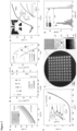
- FIG. 1 shows continuous TMD ML films and shows their wafer-scale homogeneity and intrinsic optical properties.
- the photos of MoS 2 ( Figure 1a ; greenish yellow) and WS 2 ( Figure 1b ; yellow) films grown on a transparent 4-inch fused silica wafer show that the TMD grown region (right half) is uniform over the whole substrate and clearly distinguishable from the bare silica substrate (left half).
- the optical absorption, photoluminescence (PL), and Raman spectra measured from our films show characteristics unique to ML MoS 2 and WS 2 , respectively ( Figure 1d-f ). All of these measured spectra have the same peak positions as in exfoliated ML samples (denoted by diamonds), regardless of the location of the measurements within our films ( Figure 5 ).
- the X-ray photoelectron spectra (XPS) taken from our ML MoS 2 film show almost identical features as in bulk single crystal with low level of defects, further confirming the precise chemical composition and the high quality of our MoS 2 film ( Figure 6 ).
- Figure 1c shows a photo of a MoS 2 film grown on a 4-inch SiO 2 /Si wafer.
- the ML film was patterned using standard photolithography and oxygen plasma etching to form MoS 2 covered squares (dark, 6 mm wide) with an array of 3 ⁇ m holes.
- a zoomed-in, normalized optical reflection image ( Figure 1h ) displays a homogeneous reflection contrast for the entire MoS 2 covered region, confirming uniform ML growth everywhere with no gaps.
- Figure 1g shows a scanning electron microscope (SEM) image of an array of fully-suspended ML MoS 2 membranes (2 ⁇ m in diameter) fabricated by transferring our MOCVD-grown film onto a SiN grid with holes.
- SEM scanning electron microscope
- Figure 2a schematically explains our MOCVD growth, where gas-phase precursors of Mo(CO) 6 , W(CO) 6 , (C 2 H 5 ) 2 S, and H 2 , all diluted in Ar as a carrier gas are used.
- concentration of each reactant can be precisely controlled during the entire growth time by regulating the partial pressure (Px) of each reactant (X).
- Px partial pressure
- the MoS 2 film is grown in the layer-by-layer growth mode, which is important for the uniform layer control over large scale.
- the grain structure of our MoS 2 film depends sensitively on the concentrations of H 2 , (C 2 H 5 ) 2 S as well as residual water.
- Figure 2d shows the two main effects of H 2 , whose presence is necessary for removing carbonaceous species generated during the MOCVD growth: (i) the average grain size increases from hundreds of nm to over 10 ⁇ m with decreasing H 2 flow, and (ii) the MoS 2 grains grown under higher H 2 flow ( Figure 2d , right image) have mostly perfect triangular shapes without merging with neighbouring grains, a trend that disappears with lower H 2 flow (left and middle images).
- the darkfield transmission electron microscope (DF-TEM) and annular darkfield scanning TEM (ADF-STEM) images shown in Figure 2e and 2f confirm the structural continuity of our MoS 2 film grown under those conditions on the nanometre and atomic length scales.
- the DF-TEM image shows a continuous polycrystalline ML film with no visible gaps, while having less than 0.5% bilayer area.
- Further analysis of the DF-TEM and electron diffraction data confirms a uniform angular distribution of crystal orientations with no preferred intergrain tilt angle for grain boundaries.
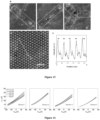
- the ADF-STEM data ( Figure 2f , more images shown in Figure 13 ) further confirm that adjacent grains are likely to be connected by a high quality lateral connection with similar structures seen in previous reports.
- ⁇ FE of the devices is compared with the results of multiple devices from two previous reports, each measured from individual grains of exfoliated or CVD grown MoS 2 samples.
- ⁇ FE measured from our MOCVD film is similar to the median ⁇ FE (denoted by a star) of exfoliated samples (and several times higher than the CVD results), while displaying a much narrower distribution.
- Figure 3d shows a high-performance MoS 2 FET fabricated with an individual top-gate electrode (V TG ). It has a high on/off conductance ratio ( ⁇ 10 6 ), current saturation at relatively low bias V SD (lower inset, Figure 3d ), high field effect mobility ( ⁇ 29 cm 2 /Vs) and large transconductance ( ⁇ 2 ⁇ S/ ⁇ m), all of which are comparable to the best reported results.
- the devices studied in Figure 3a-3d were fabricated at random locations using a polycrystalline ML MoS 2 film, unlike the devices with single-grain samples used for comparison.
- FIG. 3f shows a photo of 8, 100 MoS 2 FETs with a global back gate, which were fabricated on a 4-inch SiO 2 /Si wafer using a standard photolithography process.
- An almost perfect device yield of 99% was observed, only two out of 200 FETs we characterized (including data from an adjacent region) do not conduct.
- the data also confirm the spatially uniform n-type transistor operation (larger ⁇ ⁇ for positive V BG ) with similar V BG dependence for all our devices and high on-state device conductance.
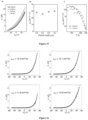
- uniform V BG dependence from FET devices fabricated using ML MoS 2 films with different average grain sizes was also observed, as characterized by the histograms of the threshold voltages ( Figure 17 ).
- 100 individually addressable dual gate MoS 2 FETs were fabricated on another wafer piece.
- Figure 4 this potential was demonstrated by producing multi-stacked ML MoS 2 films as well as electronic devices fabricated at different vertical levels.
- Figure 4a shows the schematics and photos of three substrates each with single, double or triple ML MoS 2 films grown at different levels.
- the first (bottom) ML film was grown on a fused silica substrate while the additional layers were grown on SiO 2 (100 nm thick) deposited on the previously grown MoS 2 ML using plasma-enhanced CVD (PECVD).
- PECVD plasma-enhanced CVD
- Figure 4c shows the schematics of our multi-stacked device fabrication process: (i) first ML MoS 2 growth on a SiO 2 /Si wafer, (ii) FET fabrication, (iii) deposition of SiO 2 (thickness of 500nm), (iv) second ML MoS 2 growth and FET fabrication.
- a false-colour SEM image in Figure 4d shows an array of MoS 2 FETs successfully fabricated using this process. It includes functioning MoS 2 FETs located at two different vertical levels, the conductance of which can be simultaneously modulated with a global back gate.
- the I SD -V SD curves measured from two adjacent FETs located next to each other, both laterally and vertically are shown in Figure 4e .
- Both devices show V BG dependent conductance change (notice the smaller change for the 2 nd layer) with an on-state ⁇ ⁇ of 2.5 ⁇ S (1 st layer) and 1.5 ⁇ S (2 nd layer), respectively. Furthermore, similar ⁇ FE values (11.5 cm 2 /Vs and 8.8 cm 2 /Vs) from the two devices ( Figure 19 ) were measured.
- the two ML MoS 2 films were grown on SiO 2 substrates prepared differently and that the 1 st layer device has gone through additional steps, including the second MoS 2 growth.
- the data in Figure 4 thus confirm the compatibility of the instant MOCVD-grown MoS 2 films with conventional thin film deposition and multi-stacking, which could be used to develop a three-dimensional device architecture based on TMD.
- the high-mobility ML TMD films can be immediately utilized for the batch fabrication of TMD-based integrated circuitry consisting of FETs, photodetectors and light emitting diodes, on a technologically-relevant multi-inch wafer scale.
- MOCVD growth is controlled by the kinetics of precursor supply rather than specific precursor/substrate chemistry (an example of the latter would be the different graphene growth modes on Cu vs Ni)
- its use is not limited to the TMD/substrate combinations reported here. Instead, it could be generalized for producing various TMD materials, both semiconductor (e.g. MoSe 2 , WTe 2 ) and metal (e.g. NbSe 2 , TaS 2 ), with precise layer control over a large scale.
- the data show that, as an initial demonstration, the ML TMD growth is possible on a variety of other technologically important substrates (Al 2 O 3 , SiN, HfO 2 ) with the same growth conditions developed for SiO 2 (see Figure 20 for MoS 2 growth and device fabrication on these substrates using these unoptimized conditions). Therefore, the versatile MOCVD growth provides an exciting new avenue for the growth, patterning and integration of multiple, high-quality ML TMD films with different compositions and electrical properties on a single substrate, enabling the future development of atomically thin integrated circuitry.
- MOCVD growth of ML MoS 2 and WS 2 films MOCVD growth of ML MoS 2 and WS 2 films.
- the synthesis of ML MoS 2 and WS 2 was carried out in a 4.3-inch (inner diameter) hot-wall quartz tube furnace.
- Molybdenum hexacarbonyl (MHC), tungsten hexacarbonyl (THC), diethyl sulphide (DES), which have high equilibrium vapour pressure near room temperature, are selected as chemical precursors for Mo, W, S, respectively, and introduced to the furnace in gas phase.
- H 2 and Ar are injected to the chamber using separate lines.
- MHC Sigma Aldrich 577766
- THC Sigma Aldrich 472956
- DES Sigma Aldrich 107247
- the safety ratings for these precursors require them to be handled inside of a fume hood.
- MHC, THC NFPA rating for health hazard 4
- DES NFPA rating for health hazard 2
- the optimum growth parameters for ML MoS 2 and WS 2 films are as follows. We use a total pressure of 999.92 Pa (7.5 Torr), growth temperature of 550 °C and growth time ( t 0 ) of 26 hrs.
- the flow rate of precursors are 0.01 sccm for MHC or THC, 0.4 sccm for DES, 5 sccm for H 2 , and 150 sccm for Ar, which were regulated by individual mass flow controllers (MFCs).
- MFCs mass flow controllers
- the low flow rates were used for MHC, THC and DES for the layer-by-layer growth mode.
- the long growth time ( t 0 ⁇ 26 hrs), is necessary for full ML growth, because of the low growth rate in this regime.
- NaCl is loaded in the upstream region of the furnace as a desiccant to dehydrate the growth chamber, which significantly increases the grain size, as discussed in Figure 10 .
- Optical absorption The absorption measurements were performed with a Shimadzu UV-Vis-NIR Spectrometer under ambient conditions. All measured samples were grown on a fused silica substrate, and a bare fused silica substrate was used as the reference.
- Photoluminescence The photoluminescence (PL) measurements were performed with a 532 nm excitation laser under ambient conditions.
- the PL spectra from the sample were collected by an imaging spectrometer with a CCD camera, and the PL images were taken directly using band pass filters with the centre wavelength corresponding to 1.9eV for MoS 2 and 2.0 eV for WS 2 .
- DF-TEM DF-TEM images, along with electron diffraction patterns, were taken using an FEI Tecnai T12 Spirit, operated at 80 keV. The acquisition time for each dark field image was 10 seconds.
- ADF-STEM ADF-STEM images were taken using a Nion Ultra STEM 100 operated at 60 keV. The convergence angle was 30 mrad, and the probe current was about 50 pA.
- the process was started with an as-grown ML TMD film on 285 nm SiO 2 /Si and first define the source and drain electrodes using the standard photolithography process, followed by e-beam evaporation of 0.5 nm Ti/75 nm Au. After lifting off using Microposit Remover 1165, the conducting channel for FET devices were defined and etched using photolithography and O 2 plasma etching.
- top gate fabrication 30 nm HfO 2 is deposited using atomic layer deposition (ALD) as the dielectric material, followed by the same electrode fabrication process for top-gate electrode fabrication (for top gate WS 2 FETs, we deposit 1 nm Al 2 O 3 as the seeding layer for HfO 2 ALD). 30 nm HfO 2 was deposited on top of the back gated devices. This increases the carrier doping level and the conductance of our devices, enabling reproducible measurements under ambient conditions (see Figure 21 ). All devices shown in Figure 3 and 4 were fabricated using standard photolithography techniques, except for the additional voltage probes (the five thin electrodes in Figure 3a , inset) which were added later using e-beam lithography.
- ALD atomic layer deposition
- the dimensions (W, width and L, length) of conducting channels are as follows: W 15 ⁇ m ( Figure 3a-3c ), W 9 ⁇ m, L 19 ⁇ m ( Figure 3d and 3g ), W 7.7 ⁇ m, L 3.3 ⁇ m ( Figure 3e ), W 7.7 ⁇ m, L 5.3 ⁇ m ( Figure 3f ), W 15 ⁇ m, L 15 ⁇ m ( Figure 4d and 4e ).
- the SiO 2 consists of three successive depositions: 100 nm SiO 2 was deposited using PECVD at 30 W and 200 °C, followed by 350 nm SiO 2 deposited using PECVD at 140 W and 350 °C, and 50 nm SiO 2 deposited using ALD at 200 °C.
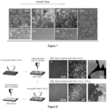
- FIG. 7 presents optical reflection (OR), PL and SEM images taken from our MOCVD grown ML MoS 2 films (average grain size ⁇ 3 ⁇ m) after different growth times (0.8 t 0 , 1.0 t 0 , and 1.5 t 0 ). It confirms that additional nucleation on the existing first layer does not occur until the first layer growth is completed and the growth proceeds by enlarging the already-nucleated grains for t ⁇ t 0 , most likely by edge attachment growth. After t 0 (full first layer growth), the nucleation for the second layer occurs at the grain boundaries (GBs) and in the basal plane.
- OR optical reflection
- PL and SEM images taken from our MOCVD grown ML MoS 2 films (average grain size ⁇ 3 ⁇ m) after different growth times (0.8 t 0 , 1.0 t 0 , and 1.5 t 0 ). It confirms that additional nucleation on the existing first layer does not occur until the first layer growth is completed and the growth proceeds
- ML direct bandgap
- indirect bandgap for multilayers
- edge attachment growth mechanism for our MOCVD growth is further supported by Figure 8 .
- step I a partial growth of ML MoS 2
- step II re-growth
- the same film was characterized by optical reflection, PL, DF-TEM after each growth step to observe the location and morphologies of the growth.
- the data confirm that during the re-growth, MoS 2 grains continue to grow by edge attachment without generating additional nucleation sites on available SiO 2 surfaces.
- step II This is confirmed by the same average number of nuclei (or grains in the first layer) per unit area after step I and step II (0.27 ⁇ m -2 ⁇ 0.26 ⁇ m -2 ), again indicating that the empty space after step I was completely filled by continued growth of existing grains (along their edges) with the same crystal orientation without creating additional grains.
Landscapes
- Chemical & Material Sciences (AREA)
- Engineering & Computer Science (AREA)
- Materials Engineering (AREA)
- Metallurgy (AREA)
- Organic Chemistry (AREA)
- General Chemical & Material Sciences (AREA)
- Chemical Kinetics & Catalysis (AREA)
- Crystallography & Structural Chemistry (AREA)
- Inorganic Chemistry (AREA)
- Mechanical Engineering (AREA)
- Chemical Vapour Deposition (AREA)
- Thin Film Transistor (AREA)
Claims (7)
- Verfahren zur Herstellung eines Metallchalkogenidfilms auf einem Substrat, wobei der Film 1 bis 10 Monoschichten eines Metallchalkogenids umfasst, wobei der Film kristallin ist, der Film eine Korngröße von 100 nm bis 100 Mikron aufweist, die Körner an den Korngrenzen lateral verbunden sind, der Film strukturell und elektrisch kontinuierlich ist und der Film über 95 % oder mehr des Substrats, das durch den Film bedeckt wird, kontinuierlich ist; wobei das Verfahren umfasst:Inkontaktbringen eines Metallvorläufers, eines Chalkogenidvorläufers, eines reduzierenden Gases und eines Substrats in einem Reaktor, so dass der Metallchalkogenidfilm gebildet wird,wobei die Vorläufer in der Gasphase vorliegen und der Metallvorläufer bei einem Druck von 1,33 Pa (1 × 10⁻² Torr) oder weniger vorliegt und der Chalkogenidvorläufer bei einem Druck von 13,33 Pa (1 × 10⁻¹ Torr) oder weniger vorliegt, wobei das Inkontaktbringen in Gegenwart eines Trocknungsmittels durchgeführt wird.
- Verfahren nach Anspruch 1, wobei das Inkontaktbringen bei einem Wasserdruck von weniger als 1,33 Pa (1 × 10⁻² Torr) durchgeführt wird.
- Verfahren nach Anspruch 1, wobei das Metall Sc, Ti, V, Cr, Mn, Fe, Co, Ni, Nb, Mo, W oder eine Kombination davon ist.
- Verfahren nach Anspruch 1 oder Anspruch 3, wobei das Chalkogenid Sulfid, Selenid, Tellurid oder eine Kombination davon ist.
- Verfahren nach einem der Ansprüche 1, 3 oder 4, wobei der Film 2 bis 10 Monoschichten eines Metallchalkogenids umfasst.
- Verfahren nach einem der Ansprüche 1, 3, 4 oder 5, wobei das Substrat eine Faser ist.
- Verfahren nach 1, 3, 4, 5 oder 6, wobei das Substrat Silicium, Silicium mit einer Siliciumoxidschicht oder Siliciumdioxidschicht, die auf mindestens einem Teil einer Oberfläche des Siliciums angeordnet ist, Quarz, Quarzglas, Glimmer, Siliciumnitrid, Bornitrid, Aluminiumoxid oder Hafniumoxid ist.
Applications Claiming Priority (1)
| Application Number | Priority Date | Filing Date | Title |
|---|---|---|---|
| US201562148387P | 2015-04-16 | 2015-04-16 |
Publications (2)
| Publication Number | Publication Date |
|---|---|
| EP3082152A1 EP3082152A1 (de) | 2016-10-19 |
| EP3082152B1 true EP3082152B1 (de) | 2023-07-19 |
Family
ID=55806167
Family Applications (1)
| Application Number | Title | Priority Date | Filing Date |
|---|---|---|---|
| EP16165628.5A Active EP3082152B1 (de) | 2015-04-16 | 2016-04-15 | Einschichtfilme aus halbleitenden metalldichalcogeniden, verfahren zur herstellung davon und verwendungen davon |
Country Status (4)
| Country | Link |
|---|---|
| US (2) | US10325987B2 (de) |
| EP (1) | EP3082152B1 (de) |
| KR (1) | KR102579500B1 (de) |
| CN (1) | CN106048556B (de) |
Families Citing this family (29)
| Publication number | Priority date | Publication date | Assignee | Title |
|---|---|---|---|---|
| US9640391B2 (en) * | 2015-06-23 | 2017-05-02 | The Trustees Of The Stevens Institute Of Technology | Direct and pre-patterned synthesis of two-dimensional heterostructures |
| US10097281B1 (en) | 2015-11-18 | 2018-10-09 | Hypres, Inc. | System and method for cryogenic optoelectronic data link |
| WO2017218488A1 (en) | 2016-06-13 | 2017-12-21 | Cornell University | Apparatuses with atomically-thin ohmic edge contacts between two-dimensional materials, methods of making same, and devices comprising same |
| US10453744B2 (en) | 2016-11-23 | 2019-10-22 | Entegris, Inc. | Low temperature molybdenum film deposition utilizing boron nucleation layers |
| GB201701109D0 (en) * | 2017-01-23 | 2017-03-08 | Univ Manchester | Method |
| US10263107B2 (en) * | 2017-05-01 | 2019-04-16 | The Regents Of The University Of California | Strain gated transistors and method |
| KR102184699B1 (ko) * | 2017-12-13 | 2020-12-01 | 한양대학교 에리카산학협력단 | 전이금속-디칼코게나이드 박막, 및 그 제조 방법 |
| WO2019125994A1 (en) * | 2017-12-18 | 2019-06-27 | Northwestern University | Multi-terminal memtransistors, fabricating methods and applications of same |
| CN110098104B (zh) * | 2018-01-20 | 2021-01-26 | 清华大学 | 一种图案化的二维过渡金属硫属化合物纳米材料的制备方法 |
| KR20200126428A (ko) | 2018-03-27 | 2020-11-06 | 코닝 인코포레이티드 | 박막 트랜지스터를 유리 기판 상에 형성하는 방법 및 이로부터 형성된 액정 디스플레이 |
| CN108666375B (zh) * | 2018-04-20 | 2019-08-13 | 华中科技大学 | 一种纳米层状横向同质pn二极管及其制备方法与应用 |
| US11021793B2 (en) * | 2018-05-31 | 2021-06-01 | L'Air Liquide, Société Anonyme pour I'Etude et I'Exploitation des Procédés Georges Claude | Group 6 transition metal-containing compositions for vapor deposition of group 6 transition metal-containing films |
| CN110510865B (zh) * | 2019-08-29 | 2022-01-25 | 上海理工大学 | 一种在微纳光纤表面制备的单层二维材料及其光活化方法 |
| CN110767533B (zh) * | 2019-10-24 | 2022-05-24 | 华南理工大学 | 一种晶圆级MoS2单层薄膜的制备方法 |
| US11430666B2 (en) | 2019-12-31 | 2022-08-30 | Taiwan Semiconductor Manufacturing Co., Ltd. | Semiconductor device and method of manufacturing semiconductor device |
| CN111420684B (zh) * | 2020-03-26 | 2022-09-13 | 内蒙古大学 | 一种合成气直接制乙醇的催化剂及应用 |
| CN112458430B (zh) * | 2020-12-09 | 2023-03-28 | 中国电子科技集团公司第四十六研究所 | 一种改善硫化钨连续膜均匀性的方法 |
| KR102473622B1 (ko) * | 2021-06-07 | 2022-12-02 | 한국과학기술연구원 | 뉴로모픽 컴퓨팅 시스템에 사용되는 플래시 메모리 장치 |
| CN113745957B (zh) * | 2021-07-27 | 2022-12-06 | 西安邮电大学 | 一种基于ws2的可饱和吸收体的制备方法 |
| KR20230030347A (ko) | 2021-08-25 | 2023-03-06 | 삼성전자주식회사 | 2차원 물질을 포함하는 전자 소자 및 그 제조 방법 |
| KR102943189B1 (ko) | 2021-09-08 | 2026-03-23 | 삼성전자주식회사 | 수직 채널 어레이 트랜지스터 구조체 및 이를 포함하는 dram 소자 |
| CN114497279B (zh) * | 2022-01-13 | 2023-07-28 | 电子科技大学 | 一种高性能光电探测器的制备方法 |
| KR20230151672A (ko) | 2022-04-26 | 2023-11-02 | 한국과학기술원 | 전이금속칼코겐막 제조방법 및 이를 위한 촉진자 |
| CN114910436B (zh) * | 2022-05-16 | 2025-07-08 | 青岛大学 | 二硫化钼微球有序阵列的光电气体传感器及其制备方法和应用 |
| PL442275A1 (pl) * | 2022-09-14 | 2024-03-18 | Politechnika Warszawska | Sposób selektywnego wzrostu heterostruktur van der Waalsa na podłożu grafenowym metodą chemicznego osadzania z fazy gazowej z wykorzystaniem naświetlania wiązką elektronową oraz heterostruktura wytworzona tym sposobem |
| WO2024145255A1 (en) * | 2022-12-28 | 2024-07-04 | Intermolecular, Inc. | Doping control in tmd (transition metal dichalcogenide) films |
| US12618146B2 (en) | 2023-09-14 | 2026-05-05 | The University Of Hong Kong | System and method for forming large-area electronic-grade metal chalcogen thin films |
| FR3156452A1 (fr) | 2023-12-06 | 2025-06-13 | Commissariat A L'energie Atomique Et Aux Energies Alternatives | Procédé de dépôt d’une couche mince de sulfure d’un métal de transition ou d’un de ses alliages |
| CN118390158B (zh) | 2024-04-23 | 2025-03-04 | 北京科技大学 | 一种二维二硫化钼材料的制备方法和应用 |
Family Cites Families (7)
| Publication number | Priority date | Publication date | Assignee | Title |
|---|---|---|---|---|
| FR2934365B1 (fr) * | 2008-07-25 | 2010-08-13 | Thales Sa | Capteur a fibre optique auto-reference a diffusion brillouin stimulee |
| JP2012114251A (ja) * | 2010-11-25 | 2012-06-14 | Kyocera Corp | 光電変換装置の製造方法 |
| US20150083206A1 (en) | 2012-03-22 | 2015-03-26 | The University Of Manchester | Photovoltaic cells |
| US8741688B2 (en) * | 2012-07-24 | 2014-06-03 | Micron Technology, Inc. | Methods of forming a metal chalcogenide material |
| US9580834B2 (en) | 2013-03-11 | 2017-02-28 | William Marsh Rice University | Growth methods for controlled large-area fabrication of high-quality graphene analogs |
| US20150118487A1 (en) | 2013-10-25 | 2015-04-30 | Colin A. Wolden | Plasma-assisted nanofabrication of two-dimensional metal chalcogenide layers |
| GB201401715D0 (en) | 2014-01-31 | 2014-03-19 | Univ Manchester | Exfoliation |
-
2016
- 2016-04-15 EP EP16165628.5A patent/EP3082152B1/de active Active
- 2016-04-15 US US15/130,407 patent/US10325987B2/en active Active
- 2016-04-15 KR KR1020160046063A patent/KR102579500B1/ko active Active
- 2016-04-18 CN CN201610238135.0A patent/CN106048556B/zh active Active
-
2019
- 2019-06-17 US US16/443,459 patent/US20190378898A1/en not_active Abandoned
Non-Patent Citations (4)
| Title |
|---|
| AREND M. VAN DER ZANDE ET AL: "Grains and grain boundaries in highly crystalline monolayer molybdenum disulphide", NATURE MATERIALS, vol. 12, no. 6, 5 May 2013 (2013-05-05), London, pages 554 - 561, XP055220725, ISSN: 1476-1122, DOI: 10.1038/nmat3633 * |
| SINA NAJMAEI ET AL: "Electrical Transport Properties of Polycrystalline Monolayer Molybdenum Disulfide", ACS NANO, vol. 8, no. 8, 26 August 2014 (2014-08-26), US, pages 7930 - 7937, XP055719988, ISSN: 1936-0851, DOI: 10.1021/nn501701a * |
| V. KRANTHI KUMAR ET AL: "A predictive approach to CVD of crystalline layers of TMDs: the case of MoS 2", NANOSCALE, vol. 7, no. 17, 25 March 2015 (2015-03-25), United Kingdom, pages 7802 - 7810, XP055381511, ISSN: 2040-3364, DOI: 10.1039/C4NR07080A * |
| V. KRANTHI KUMAR ET AL: "Supporting Information: Predictive approach to CVD of crystalline layers of TMDs: the case of MoS 2", NANOSCALE, vol. 7, no. 17, 25 March 2015 (2015-03-25), XP055381509 * |
Also Published As
| Publication number | Publication date |
|---|---|
| US20190378898A1 (en) | 2019-12-12 |
| US20160308006A1 (en) | 2016-10-20 |
| CN106048556B (zh) | 2021-06-22 |
| KR102579500B1 (ko) | 2023-09-19 |
| CN106048556A (zh) | 2016-10-26 |
| EP3082152A1 (de) | 2016-10-19 |
| US10325987B2 (en) | 2019-06-18 |
| KR20160124017A (ko) | 2016-10-26 |
Similar Documents
| Publication | Publication Date | Title |
|---|---|---|
| US10325987B2 (en) | Monolayer films of semiconducting metal dichalcogenides, methods of making same, and uses of same | |
| Sun et al. | Chemical vapour deposition | |
| Cun et al. | Wafer-scale MOCVD growth of monolayer MoS2 on sapphire and SiO2 | |
| Wong et al. | Recent progress in chemical vapor deposition growth of two-dimensional transition metal dichalcogenides | |
| Shi et al. | Engineering wafer-scale epitaxial two-dimensional materials through sapphire template screening for advanced high-performance nanoelectronics | |
| US10465276B2 (en) | Facile route to templated growth of two-dimensional layered materials | |
| US10309011B2 (en) | Method for manufacturing two-dimensional transition metal dichalcogemide thin film | |
| Han et al. | Seeded growth of highly crystalline molybdenum disulphide monolayers at controlled locations | |
| US10910473B2 (en) | Apparatuses with atomically-thin ohmic edge contacts between two-dimensional materials, methods of making same, and devices comprising same | |
| KR20180075898A (ko) | 그래핀 상 금속산화물층의 형성방법, 그에 의해 제조된 그래핀 상 금속산화물층 및 그래핀 상 금속산화물층을 포함하는 전자소자 | |
| KR20150098904A (ko) | 금속 칼코게나이드 박막의 제조 방법 및 그 박막 | |
| US12426406B2 (en) | Dislocation free semiconductor nanostructures grown by pulse laser deposition with no seeding or catalyst | |
| KR102280763B1 (ko) | 전이금속 디칼코게나이드 박막, 그 제조 방법 및 제조 장치 | |
| Vergnaud et al. | Van der Waals solid phase epitaxy to grow large-area manganese-doped MoSe2 few-layers on SiO2/Si | |
| EP4427261A1 (de) | Verfahren zum selektiven wachstum von van-der-waals-heterostrukturen auf einem graphensubstrat durch chemische dampfabscheidung mit elektronenbestrahlung und mit diesem verfahren hergestellte heterostruktur | |
| Singh | Fabrication Approaches of TMDs | |
| Portone et al. | Deterministic synthesis of Cu 9 S 5 flakes assisted by single-layer graphene arrays | |
| KR102690300B1 (ko) | 전이금속 칼코젠 화합물 및 그 제조방법 | |
| US20250389052A1 (en) | Novel synthesis of two-dimensional indium selenide | |
| 문동훈 | Hypotaxy for fabrication of single crystal 2D materials and their moiré structures | |
| Chrysler | Charge Transfer and Built-In Fields at a Semiconductor-Crystalline Oxide Interface: Effects of the Interface Dipole and Surface Termination | |
| Kozhakhmetov | MOCVD Synthesis and Doping of FRONT-END-OF-LINE (FEOL) and BACK-END-OF-LINE (BEOL) Compatible Two-Dimensional WSe2 | |
| Wu | Highly Kinetic Deposition Technique and Phase Engineering of 2D Transition Metal Dichalcogendies, Janus Structures, and Next-Generation High-Mobility Semiconductors | |
| Palczyński | Characterisation of atomically-thin transition metal dichalcogenides | |
| Subramanian | Engineering Epitaxial Graphene-based 2D Heterojunctions for Electronic and Optoelectronic Applications |
Legal Events
| Date | Code | Title | Description |
|---|---|---|---|
| PUAI | Public reference made under article 153(3) epc to a published international application that has entered the european phase |
Free format text: ORIGINAL CODE: 0009012 |
|
| AK | Designated contracting states |
Kind code of ref document: A1 Designated state(s): AL AT BE BG CH CY CZ DE DK EE ES FI FR GB GR HR HU IE IS IT LI LT LU LV MC MK MT NL NO PL PT RO RS SE SI SK SM TR |
|
| AX | Request for extension of the european patent |
Extension state: BA ME |
|
| STAA | Information on the status of an ep patent application or granted ep patent |
Free format text: STATUS: REQUEST FOR EXAMINATION WAS MADE |
|
| 17P | Request for examination filed |
Effective date: 20170419 |
|
| RBV | Designated contracting states (corrected) |
Designated state(s): AL AT BE BG CH CY CZ DE DK EE ES FI FR GB GR HR HU IE IS IT LI LT LU LV MC MK MT NL NO PL PT RO RS SE SI SK SM TR |
|
| STAA | Information on the status of an ep patent application or granted ep patent |
Free format text: STATUS: EXAMINATION IS IN PROGRESS |
|
| 17Q | First examination report despatched |
Effective date: 20170717 |
|
| RAP1 | Party data changed (applicant data changed or rights of an application transferred) |
Owner name: CORNELL UNIVERSITY |
|
| REG | Reference to a national code |
Ref country code: DE Ref legal event code: R079 Free format text: PREVIOUS MAIN CLASS: H01L0021020000 Ipc: H01L0021205000 Ref country code: DE Ref legal event code: R079 Ref document number: 602016081116 Country of ref document: DE Free format text: PREVIOUS MAIN CLASS: H01L0021020000 Ipc: H01L0021205000 |
|
| GRAP | Despatch of communication of intention to grant a patent |
Free format text: ORIGINAL CODE: EPIDOSNIGR1 |
|
| STAA | Information on the status of an ep patent application or granted ep patent |
Free format text: STATUS: GRANT OF PATENT IS INTENDED |
|
| RIC1 | Information provided on ipc code assigned before grant |
Ipc: H01L 21/02 20060101ALI20230124BHEP Ipc: H01L 21/20 20060101ALI20230124BHEP Ipc: H01L 21/205 20060101AFI20230124BHEP |
|
| INTG | Intention to grant announced |
Effective date: 20230214 |
|
| GRAS | Grant fee paid |
Free format text: ORIGINAL CODE: EPIDOSNIGR3 |
|
| GRAA | (expected) grant |
Free format text: ORIGINAL CODE: 0009210 |
|
| STAA | Information on the status of an ep patent application or granted ep patent |
Free format text: STATUS: THE PATENT HAS BEEN GRANTED |
|
| P01 | Opt-out of the competence of the unified patent court (upc) registered |
Effective date: 20230519 |
|
| AK | Designated contracting states |
Kind code of ref document: B1 Designated state(s): AL AT BE BG CH CY CZ DE DK EE ES FI FR GB GR HR HU IE IS IT LI LT LU LV MC MK MT NL NO PL PT RO RS SE SI SK SM TR |
|
| REG | Reference to a national code |
Ref country code: GB Ref legal event code: FG4D |
|
| REG | Reference to a national code |
Ref country code: CH Ref legal event code: EP |
|
| REG | Reference to a national code |
Ref country code: DE Ref legal event code: R096 Ref document number: 602016081116 Country of ref document: DE |
|
| REG | Reference to a national code |
Ref country code: IE Ref legal event code: FG4D |
|
| REG | Reference to a national code |
Ref country code: LT Ref legal event code: MG9D |
|
| REG | Reference to a national code |
Ref country code: NL Ref legal event code: MP Effective date: 20230719 |
|
| REG | Reference to a national code |
Ref country code: AT Ref legal event code: MK05 Ref document number: 1590357 Country of ref document: AT Kind code of ref document: T Effective date: 20230719 |
|
| PG25 | Lapsed in a contracting state [announced via postgrant information from national office to epo] |
Ref country code: NL Free format text: LAPSE BECAUSE OF FAILURE TO SUBMIT A TRANSLATION OF THE DESCRIPTION OR TO PAY THE FEE WITHIN THE PRESCRIBED TIME-LIMIT Effective date: 20230719 |
|
| PG25 | Lapsed in a contracting state [announced via postgrant information from national office to epo] |
Ref country code: GR Free format text: LAPSE BECAUSE OF FAILURE TO SUBMIT A TRANSLATION OF THE DESCRIPTION OR TO PAY THE FEE WITHIN THE PRESCRIBED TIME-LIMIT Effective date: 20231020 |
|
| PG25 | Lapsed in a contracting state [announced via postgrant information from national office to epo] |
Ref country code: IS Free format text: LAPSE BECAUSE OF FAILURE TO SUBMIT A TRANSLATION OF THE DESCRIPTION OR TO PAY THE FEE WITHIN THE PRESCRIBED TIME-LIMIT Effective date: 20231119 |
|
| PG25 | Lapsed in a contracting state [announced via postgrant information from national office to epo] |
Ref country code: SE Free format text: LAPSE BECAUSE OF FAILURE TO SUBMIT A TRANSLATION OF THE DESCRIPTION OR TO PAY THE FEE WITHIN THE PRESCRIBED TIME-LIMIT Effective date: 20230719 Ref country code: RS Free format text: LAPSE BECAUSE OF FAILURE TO SUBMIT A TRANSLATION OF THE DESCRIPTION OR TO PAY THE FEE WITHIN THE PRESCRIBED TIME-LIMIT Effective date: 20230719 Ref country code: PT Free format text: LAPSE BECAUSE OF FAILURE TO SUBMIT A TRANSLATION OF THE DESCRIPTION OR TO PAY THE FEE WITHIN THE PRESCRIBED TIME-LIMIT Effective date: 20231120 Ref country code: NO Free format text: LAPSE BECAUSE OF FAILURE TO SUBMIT A TRANSLATION OF THE DESCRIPTION OR TO PAY THE FEE WITHIN THE PRESCRIBED TIME-LIMIT Effective date: 20231019 Ref country code: LV Free format text: LAPSE BECAUSE OF FAILURE TO SUBMIT A TRANSLATION OF THE DESCRIPTION OR TO PAY THE FEE WITHIN THE PRESCRIBED TIME-LIMIT Effective date: 20230719 Ref country code: LT Free format text: LAPSE BECAUSE OF FAILURE TO SUBMIT A TRANSLATION OF THE DESCRIPTION OR TO PAY THE FEE WITHIN THE PRESCRIBED TIME-LIMIT Effective date: 20230719 Ref country code: IS Free format text: LAPSE BECAUSE OF FAILURE TO SUBMIT A TRANSLATION OF THE DESCRIPTION OR TO PAY THE FEE WITHIN THE PRESCRIBED TIME-LIMIT Effective date: 20231119 Ref country code: HR Free format text: LAPSE BECAUSE OF FAILURE TO SUBMIT A TRANSLATION OF THE DESCRIPTION OR TO PAY THE FEE WITHIN THE PRESCRIBED TIME-LIMIT Effective date: 20230719 Ref country code: GR Free format text: LAPSE BECAUSE OF FAILURE TO SUBMIT A TRANSLATION OF THE DESCRIPTION OR TO PAY THE FEE WITHIN THE PRESCRIBED TIME-LIMIT Effective date: 20231020 Ref country code: FI Free format text: LAPSE BECAUSE OF FAILURE TO SUBMIT A TRANSLATION OF THE DESCRIPTION OR TO PAY THE FEE WITHIN THE PRESCRIBED TIME-LIMIT Effective date: 20230719 Ref country code: AT Free format text: LAPSE BECAUSE OF FAILURE TO SUBMIT A TRANSLATION OF THE DESCRIPTION OR TO PAY THE FEE WITHIN THE PRESCRIBED TIME-LIMIT Effective date: 20230719 |
|
| PG25 | Lapsed in a contracting state [announced via postgrant information from national office to epo] |
Ref country code: PL Free format text: LAPSE BECAUSE OF FAILURE TO SUBMIT A TRANSLATION OF THE DESCRIPTION OR TO PAY THE FEE WITHIN THE PRESCRIBED TIME-LIMIT Effective date: 20230719 |
|
| REG | Reference to a national code |
Ref country code: DE Ref legal event code: R097 Ref document number: 602016081116 Country of ref document: DE |
|
| PG25 | Lapsed in a contracting state [announced via postgrant information from national office to epo] |
Ref country code: ES Free format text: LAPSE BECAUSE OF FAILURE TO SUBMIT A TRANSLATION OF THE DESCRIPTION OR TO PAY THE FEE WITHIN THE PRESCRIBED TIME-LIMIT Effective date: 20230719 |
|
| PG25 | Lapsed in a contracting state [announced via postgrant information from national office to epo] |
Ref country code: SM Free format text: LAPSE BECAUSE OF FAILURE TO SUBMIT A TRANSLATION OF THE DESCRIPTION OR TO PAY THE FEE WITHIN THE PRESCRIBED TIME-LIMIT Effective date: 20230719 Ref country code: RO Free format text: LAPSE BECAUSE OF FAILURE TO SUBMIT A TRANSLATION OF THE DESCRIPTION OR TO PAY THE FEE WITHIN THE PRESCRIBED TIME-LIMIT Effective date: 20230719 Ref country code: ES Free format text: LAPSE BECAUSE OF FAILURE TO SUBMIT A TRANSLATION OF THE DESCRIPTION OR TO PAY THE FEE WITHIN THE PRESCRIBED TIME-LIMIT Effective date: 20230719 Ref country code: EE Free format text: LAPSE BECAUSE OF FAILURE TO SUBMIT A TRANSLATION OF THE DESCRIPTION OR TO PAY THE FEE WITHIN THE PRESCRIBED TIME-LIMIT Effective date: 20230719 Ref country code: DK Free format text: LAPSE BECAUSE OF FAILURE TO SUBMIT A TRANSLATION OF THE DESCRIPTION OR TO PAY THE FEE WITHIN THE PRESCRIBED TIME-LIMIT Effective date: 20230719 Ref country code: CZ Free format text: LAPSE BECAUSE OF FAILURE TO SUBMIT A TRANSLATION OF THE DESCRIPTION OR TO PAY THE FEE WITHIN THE PRESCRIBED TIME-LIMIT Effective date: 20230719 Ref country code: SK Free format text: LAPSE BECAUSE OF FAILURE TO SUBMIT A TRANSLATION OF THE DESCRIPTION OR TO PAY THE FEE WITHIN THE PRESCRIBED TIME-LIMIT Effective date: 20230719 |
|
| PLBE | No opposition filed within time limit |
Free format text: ORIGINAL CODE: 0009261 |
|
| STAA | Information on the status of an ep patent application or granted ep patent |
Free format text: STATUS: NO OPPOSITION FILED WITHIN TIME LIMIT |
|
| PG25 | Lapsed in a contracting state [announced via postgrant information from national office to epo] |
Ref country code: IT Free format text: LAPSE BECAUSE OF FAILURE TO SUBMIT A TRANSLATION OF THE DESCRIPTION OR TO PAY THE FEE WITHIN THE PRESCRIBED TIME-LIMIT Effective date: 20230719 |
|
| 26N | No opposition filed |
Effective date: 20240422 |
|
| PG25 | Lapsed in a contracting state [announced via postgrant information from national office to epo] |
Ref country code: SI Free format text: LAPSE BECAUSE OF FAILURE TO SUBMIT A TRANSLATION OF THE DESCRIPTION OR TO PAY THE FEE WITHIN THE PRESCRIBED TIME-LIMIT Effective date: 20230719 |
|
| PG25 | Lapsed in a contracting state [announced via postgrant information from national office to epo] |
Ref country code: BG Free format text: LAPSE BECAUSE OF FAILURE TO SUBMIT A TRANSLATION OF THE DESCRIPTION OR TO PAY THE FEE WITHIN THE PRESCRIBED TIME-LIMIT Effective date: 20230719 |
|
| PG25 | Lapsed in a contracting state [announced via postgrant information from national office to epo] |
Ref country code: MC Free format text: LAPSE BECAUSE OF FAILURE TO SUBMIT A TRANSLATION OF THE DESCRIPTION OR TO PAY THE FEE WITHIN THE PRESCRIBED TIME-LIMIT Effective date: 20230719 |
|
| PG25 | Lapsed in a contracting state [announced via postgrant information from national office to epo] |
Ref country code: MC Free format text: LAPSE BECAUSE OF FAILURE TO SUBMIT A TRANSLATION OF THE DESCRIPTION OR TO PAY THE FEE WITHIN THE PRESCRIBED TIME-LIMIT Effective date: 20230719 Ref country code: BG Free format text: LAPSE BECAUSE OF FAILURE TO SUBMIT A TRANSLATION OF THE DESCRIPTION OR TO PAY THE FEE WITHIN THE PRESCRIBED TIME-LIMIT Effective date: 20230719 |
|
| REG | Reference to a national code |
Ref country code: CH Ref legal event code: PL |
|
| PG25 | Lapsed in a contracting state [announced via postgrant information from national office to epo] |
Ref country code: LU Free format text: LAPSE BECAUSE OF NON-PAYMENT OF DUE FEES Effective date: 20240415 |
|
| REG | Reference to a national code |
Ref country code: BE Ref legal event code: MM Effective date: 20240430 |
|
| PG25 | Lapsed in a contracting state [announced via postgrant information from national office to epo] |
Ref country code: LU Free format text: LAPSE BECAUSE OF NON-PAYMENT OF DUE FEES Effective date: 20240415 |
|
| PG25 | Lapsed in a contracting state [announced via postgrant information from national office to epo] |
Ref country code: BE Free format text: LAPSE BECAUSE OF NON-PAYMENT OF DUE FEES Effective date: 20240430 |
|
| PG25 | Lapsed in a contracting state [announced via postgrant information from national office to epo] |
Ref country code: BE Free format text: LAPSE BECAUSE OF NON-PAYMENT OF DUE FEES Effective date: 20240430 Ref country code: CH Free format text: LAPSE BECAUSE OF NON-PAYMENT OF DUE FEES Effective date: 20240430 |
|
| PG25 | Lapsed in a contracting state [announced via postgrant information from national office to epo] |
Ref country code: IE Free format text: LAPSE BECAUSE OF NON-PAYMENT OF DUE FEES Effective date: 20240415 |
|
| PGFP | Annual fee paid to national office [announced via postgrant information from national office to epo] |
Ref country code: DE Payment date: 20250429 Year of fee payment: 10 |
|
| PGFP | Annual fee paid to national office [announced via postgrant information from national office to epo] |
Ref country code: GB Payment date: 20250428 Year of fee payment: 10 |
|
| PGFP | Annual fee paid to national office [announced via postgrant information from national office to epo] |
Ref country code: FR Payment date: 20250425 Year of fee payment: 10 |
|
| PG25 | Lapsed in a contracting state [announced via postgrant information from national office to epo] |
Ref country code: CY Free format text: LAPSE BECAUSE OF FAILURE TO SUBMIT A TRANSLATION OF THE DESCRIPTION OR TO PAY THE FEE WITHIN THE PRESCRIBED TIME-LIMIT; INVALID AB INITIO Effective date: 20160415 |
|
| PG25 | Lapsed in a contracting state [announced via postgrant information from national office to epo] |
Ref country code: HU Free format text: LAPSE BECAUSE OF FAILURE TO SUBMIT A TRANSLATION OF THE DESCRIPTION OR TO PAY THE FEE WITHIN THE PRESCRIBED TIME-LIMIT; INVALID AB INITIO Effective date: 20160415 |
|
| REG | Reference to a national code |
Ref country code: DE Ref legal event code: R079 Ref document number: 602016081116 Country of ref document: DE Free format text: PREVIOUS MAIN CLASS: H01L0021205000 Ipc: H10P0014240000 |