EP3080871B1 - Élément de contact - Google Patents
Élément de contact Download PDFInfo
- Publication number
- EP3080871B1 EP3080871B1 EP14808670.5A EP14808670A EP3080871B1 EP 3080871 B1 EP3080871 B1 EP 3080871B1 EP 14808670 A EP14808670 A EP 14808670A EP 3080871 B1 EP3080871 B1 EP 3080871B1
- Authority
- EP
- European Patent Office
- Prior art keywords
- contact
- making element
- contacting element
- carrier device
- section
- Prior art date
- Legal status (The legal status is an assumption and is not a legal conclusion. Google has not performed a legal analysis and makes no representation as to the accuracy of the status listed.)
- Active
Links
- 238000000034 method Methods 0.000 claims description 33
- 239000004020 conductor Substances 0.000 claims description 23
- 238000005476 soldering Methods 0.000 claims description 15
- 238000002788 crimping Methods 0.000 claims description 8
- 210000000078 claw Anatomy 0.000 claims description 4
- 238000003825 pressing Methods 0.000 claims description 4
- 102000015933 Rim-like Human genes 0.000 claims 1
- 108050004199 Rim-like Proteins 0.000 claims 1
- WABPQHHGFIMREM-UHFFFAOYSA-N lead(0) Chemical compound [Pb] WABPQHHGFIMREM-UHFFFAOYSA-N 0.000 description 9
- 229910000679 solder Inorganic materials 0.000 description 4
- 238000011161 development Methods 0.000 description 3
- 230000018109 developmental process Effects 0.000 description 3
- 238000003466 welding Methods 0.000 description 3
- 239000003990 capacitor Substances 0.000 description 2
- 230000008719 thickening Effects 0.000 description 2
- RYGMFSIKBFXOCR-UHFFFAOYSA-N Copper Chemical compound [Cu] RYGMFSIKBFXOCR-UHFFFAOYSA-N 0.000 description 1
- 230000002238 attenuated effect Effects 0.000 description 1
- 229910052802 copper Inorganic materials 0.000 description 1
- 239000010949 copper Substances 0.000 description 1
- 238000005520 cutting process Methods 0.000 description 1
- 230000001419 dependent effect Effects 0.000 description 1
- 230000000694 effects Effects 0.000 description 1
- 239000011810 insulating material Substances 0.000 description 1
- 238000009413 insulation Methods 0.000 description 1
- 238000004519 manufacturing process Methods 0.000 description 1
- 238000009877 rendering Methods 0.000 description 1
Images

Classifications
-
- H—ELECTRICITY
- H01—ELECTRIC ELEMENTS
- H01R—ELECTRICALLY-CONDUCTIVE CONNECTIONS; STRUCTURAL ASSOCIATIONS OF A PLURALITY OF MUTUALLY-INSULATED ELECTRICAL CONNECTING ELEMENTS; COUPLING DEVICES; CURRENT COLLECTORS
- H01R12/00—Structural associations of a plurality of mutually-insulated electrical connecting elements, specially adapted for printed circuits, e.g. printed circuit boards [PCB], flat or ribbon cables, or like generally planar structures, e.g. terminal strips, terminal blocks; Coupling devices specially adapted for printed circuits, flat or ribbon cables, or like generally planar structures; Terminals specially adapted for contact with, or insertion into, printed circuits, flat or ribbon cables, or like generally planar structures
- H01R12/50—Fixed connections
- H01R12/51—Fixed connections for rigid printed circuits or like structures
- H01R12/53—Fixed connections for rigid printed circuits or like structures connecting to cables except for flat or ribbon cables
-
- H—ELECTRICITY
- H01—ELECTRIC ELEMENTS
- H01R—ELECTRICALLY-CONDUCTIVE CONNECTIONS; STRUCTURAL ASSOCIATIONS OF A PLURALITY OF MUTUALLY-INSULATED ELECTRICAL CONNECTING ELEMENTS; COUPLING DEVICES; CURRENT COLLECTORS
- H01R12/00—Structural associations of a plurality of mutually-insulated electrical connecting elements, specially adapted for printed circuits, e.g. printed circuit boards [PCB], flat or ribbon cables, or like generally planar structures, e.g. terminal strips, terminal blocks; Coupling devices specially adapted for printed circuits, flat or ribbon cables, or like generally planar structures; Terminals specially adapted for contact with, or insertion into, printed circuits, flat or ribbon cables, or like generally planar structures
- H01R12/50—Fixed connections
- H01R12/51—Fixed connections for rigid printed circuits or like structures
- H01R12/55—Fixed connections for rigid printed circuits or like structures characterised by the terminals
-
- H—ELECTRICITY
- H01—ELECTRIC ELEMENTS
- H01R—ELECTRICALLY-CONDUCTIVE CONNECTIONS; STRUCTURAL ASSOCIATIONS OF A PLURALITY OF MUTUALLY-INSULATED ELECTRICAL CONNECTING ELEMENTS; COUPLING DEVICES; CURRENT COLLECTORS
- H01R12/00—Structural associations of a plurality of mutually-insulated electrical connecting elements, specially adapted for printed circuits, e.g. printed circuit boards [PCB], flat or ribbon cables, or like generally planar structures, e.g. terminal strips, terminal blocks; Coupling devices specially adapted for printed circuits, flat or ribbon cables, or like generally planar structures; Terminals specially adapted for contact with, or insertion into, printed circuits, flat or ribbon cables, or like generally planar structures
- H01R12/50—Fixed connections
- H01R12/59—Fixed connections for flexible printed circuits, flat or ribbon cables or like structures
- H01R12/63—Fixed connections for flexible printed circuits, flat or ribbon cables or like structures connecting to another shape cable
-
- H—ELECTRICITY
- H01—ELECTRIC ELEMENTS
- H01R—ELECTRICALLY-CONDUCTIVE CONNECTIONS; STRUCTURAL ASSOCIATIONS OF A PLURALITY OF MUTUALLY-INSULATED ELECTRICAL CONNECTING ELEMENTS; COUPLING DEVICES; CURRENT COLLECTORS
- H01R12/00—Structural associations of a plurality of mutually-insulated electrical connecting elements, specially adapted for printed circuits, e.g. printed circuit boards [PCB], flat or ribbon cables, or like generally planar structures, e.g. terminal strips, terminal blocks; Coupling devices specially adapted for printed circuits, flat or ribbon cables, or like generally planar structures; Terminals specially adapted for contact with, or insertion into, printed circuits, flat or ribbon cables, or like generally planar structures
- H01R12/50—Fixed connections
- H01R12/59—Fixed connections for flexible printed circuits, flat or ribbon cables or like structures
- H01R12/65—Fixed connections for flexible printed circuits, flat or ribbon cables or like structures characterised by the terminal
-
- H—ELECTRICITY
- H01—ELECTRIC ELEMENTS
- H01R—ELECTRICALLY-CONDUCTIVE CONNECTIONS; STRUCTURAL ASSOCIATIONS OF A PLURALITY OF MUTUALLY-INSULATED ELECTRICAL CONNECTING ELEMENTS; COUPLING DEVICES; CURRENT COLLECTORS
- H01R4/00—Electrically-conductive connections between two or more conductive members in direct contact, i.e. touching one another; Means for effecting or maintaining such contact; Electrically-conductive connections having two or more spaced connecting locations for conductors and using contact members penetrating insulation
- H01R4/02—Soldered or welded connections
- H01R4/023—Soldered or welded connections between cables or wires and terminals
-
- H—ELECTRICITY
- H01—ELECTRIC ELEMENTS
- H01R—ELECTRICALLY-CONDUCTIVE CONNECTIONS; STRUCTURAL ASSOCIATIONS OF A PLURALITY OF MUTUALLY-INSULATED ELECTRICAL CONNECTING ELEMENTS; COUPLING DEVICES; CURRENT COLLECTORS
- H01R4/00—Electrically-conductive connections between two or more conductive members in direct contact, i.e. touching one another; Means for effecting or maintaining such contact; Electrically-conductive connections having two or more spaced connecting locations for conductors and using contact members penetrating insulation
- H01R4/10—Electrically-conductive connections between two or more conductive members in direct contact, i.e. touching one another; Means for effecting or maintaining such contact; Electrically-conductive connections having two or more spaced connecting locations for conductors and using contact members penetrating insulation effected solely by twisting, wrapping, bending, crimping, or other permanent deformation
- H01R4/18—Electrically-conductive connections between two or more conductive members in direct contact, i.e. touching one another; Means for effecting or maintaining such contact; Electrically-conductive connections having two or more spaced connecting locations for conductors and using contact members penetrating insulation effected solely by twisting, wrapping, bending, crimping, or other permanent deformation by crimping
- H01R4/187—Electrically-conductive connections between two or more conductive members in direct contact, i.e. touching one another; Means for effecting or maintaining such contact; Electrically-conductive connections having two or more spaced connecting locations for conductors and using contact members penetrating insulation effected solely by twisting, wrapping, bending, crimping, or other permanent deformation by crimping combined with soldering or welding
-
- H—ELECTRICITY
- H01—ELECTRIC ELEMENTS
- H01R—ELECTRICALLY-CONDUCTIVE CONNECTIONS; STRUCTURAL ASSOCIATIONS OF A PLURALITY OF MUTUALLY-INSULATED ELECTRICAL CONNECTING ELEMENTS; COUPLING DEVICES; CURRENT COLLECTORS
- H01R4/00—Electrically-conductive connections between two or more conductive members in direct contact, i.e. touching one another; Means for effecting or maintaining such contact; Electrically-conductive connections having two or more spaced connecting locations for conductors and using contact members penetrating insulation
- H01R4/10—Electrically-conductive connections between two or more conductive members in direct contact, i.e. touching one another; Means for effecting or maintaining such contact; Electrically-conductive connections having two or more spaced connecting locations for conductors and using contact members penetrating insulation effected solely by twisting, wrapping, bending, crimping, or other permanent deformation
- H01R4/18—Electrically-conductive connections between two or more conductive members in direct contact, i.e. touching one another; Means for effecting or maintaining such contact; Electrically-conductive connections having two or more spaced connecting locations for conductors and using contact members penetrating insulation effected solely by twisting, wrapping, bending, crimping, or other permanent deformation by crimping
- H01R4/20—Electrically-conductive connections between two or more conductive members in direct contact, i.e. touching one another; Means for effecting or maintaining such contact; Electrically-conductive connections having two or more spaced connecting locations for conductors and using contact members penetrating insulation effected solely by twisting, wrapping, bending, crimping, or other permanent deformation by crimping using a crimping sleeve
- H01R4/203—Electrically-conductive connections between two or more conductive members in direct contact, i.e. touching one another; Means for effecting or maintaining such contact; Electrically-conductive connections having two or more spaced connecting locations for conductors and using contact members penetrating insulation effected solely by twisting, wrapping, bending, crimping, or other permanent deformation by crimping using a crimping sleeve having an uneven wire-receiving surface to improve the contact
Definitions
- the invention relates to a contacting element.
- the invention further relates to a method for electrically contacting a conductor wire with a carrier device for at least one electrical conductor track.
- Electrical connections of two or more components are usually performed by crimping, soldering, welding, etc.
- crimping soldering, welding, etc.
- the phases of the motor are electrically connected to the electronics either via soldering, welding, clamping cutting.
- electrical connection technology crimping which is used, inter alia, to electrically connect cables with plug contacts.
- the object is achieved with a contacting element according to independent claim 1.
- the object is achieved according to a second aspect with a method for electrically contacting a conductor wire with a carrier device for at least one electrical conductor, according to the independent claim 9.
- a simple contacting process for the electrical conductor wire is made possible with the contacting element according to the invention, wherein first the contacting element is electrically contacted with the carrier device. In a further process step, the actual electrical contacting process of the lead wire then takes place with the contacting element and thus with the carrier device.
- a preferred embodiment of the contacting element according to the invention is characterized in that the second portion is formed brim-shaped and is arranged transversely to the first portion.
- a form of the contacting element is created by means of which it is particularly simple to mechanically and electrically connect the contacting element to the carrier device in different ways.
- the contacting element is attached to the carrier device and electrically contacted at least one electrical conductor track.
- an electrical connection between the wires and the conductor paths can be produced inexpensively.
- a further preferred embodiment of the contacting element according to the invention is characterized in that the contacting element can be soldered to the carrier device in a soldering process.
- the contacting element can be soldered to the carrier device by means of a reflow soldering process.
- the contacting element can be soldered to the carrier device by means of a reflow soldering process.
- non-reflow-solderable components eg, electrolytic capacitors
- the contacting element comprises two half-shells which can be pressed together and with the carrier device.
- an alternative embodiment for the contacting element which is electrically and mechanically contactable in a purely mechanical manner by means of a riveting or pressing operation with the carrier device.
- a further preferred embodiment of the contacting element according to the invention is characterized in that the first portion of the contacting element in the contacted state with the carrier device at least partially has a non-uniform diameter. In this way, a strain relief for the carrier device is realized, which makes it possible to keep away mechanical forces from the carrier device or from the solder joint.
- the contacting element has at least one slot on the first section. This makes it possible that a structure of the first section is weakened, so that in a subsequent pressing operation, the contacting element is pressed with little effort with the lead wire and thus can be electrically contacted.
- An "electrical conductor wire” in the sense of the present invention comprises all elongated (ie thin in relation to its length) insulated and non-insulated electrical wires or cables, such as a copper enameled wire, a lead wire of a device (eg an electrolytic capacitor), a wire with a wire mesh, etc.
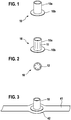
- Fig. 1 shows a perspective view of a first embodiment of the contacting element according to the invention 10.
- the contacting element 10 is electrically conductive, preferably formed metallic.
- the contacting element 10 has a first sleeve-shaped portion 10a and a second portion 10b.
- the first section 10a is provided for receiving an electrical lead wire (not shown) and mechanically and electrically connecting it to the contacting element 10 (eg by means of a crimp connection).
- the second section 10b is intended to contact the contacting element 10 electrically and mechanically with a printed circuit board (not shown).
- the first portion 10b is formed as a kind of "hat brim". This results in this way, therefore, a contacting element 10 in the form of a crimping sleeve, which consists of an electrically conductive material, and which has a brim at the lower end.
- Fig. 2 shows in an upper view, another perspective view of another embodiment of the contacting element 10 according to the invention recognizes in the first section 10a a plurality of axially extending Einschlitzonne 11, which are provided so that the structure of the first portion 10a is weakened, so that with relatively little effort the first portion 10a can be crimped by means of a crimping tool with a lead wire (not shown).
- the contacting element 10 has a plurality of claw elements 12 on its inner surface.
- FIG. 3 shows a further perspective view of the contacting element 10 in an electrical circuit board 40 (not shown). It can be seen a conductor 41, which is electrically connected to a solder pad 42, and to which the contacting element 10 is electrically contacted. In this case, the contacting element 10 is placed from above onto the printed circuit board 40 and can thus be soldered from above.
- Fig. 4 shows in a front view of an inserted into the circuit board 40 from below electrical contacting element 10. The contacting element 10 is also here first electrically and mechanically connected to the circuit board 40, for example by a soldering process.
- the lead wire 20 is inserted or pushed through the contacting element 10 and then crimped with the contacting element 10, whereby an electrical contact with a conductor track of the circuit board 40 comes about.
- a suitable, preferably automated Krimpgins creates a kind of partial thickening in the first portion 10a of the contacting element 10, which allows a strain relief, by means of the mechanical forces of the solder joint on the circuit board 40 can be kept away that a two-sided fixation of the Contacting element 10 in the circuit board 40, namely by means of the thickening and by means of the second portion 10b is realized.
- the lead wire 30 may have a bend below or above the printed circuit board 40, whereby a kind of spring is formed, by means of which mechanical forces on the printed circuit board 40 or on the solder joint can be at least attenuated.
- the soldering process is preferably carried out in the form of a reflow soldering process in which other SMD components (surface mounted device, not shown) are also contacted mechanically and electrically on the printed circuit board 40.
- the entire contacting method of the conductor wire 20 with the circuit board 40 can be limited to a two-stage process, which consists in first soldering the contacting element 10 to the circuit board 40 and then crimping the conductor wire 20 with the contacting element 10.
- the method can be performed when contacting leads of a motor with a circuit board 40 of an engine electronics.
- the contacting element 10 can also be electrically and mechanically connected to the printed circuit board 40 by means of a riveting or pressing process.
- the contacting element 10 is formed from two half-shells (not shown), which are guided from different sides of the circuit board 40 and pressed together and with the circuit board 40.
- Fig. 6 is a basic sequence of an embodiment of the inventive method for electrically contacting a conductor wire with a carrier device for at least one electrical conductor shown.
- a first step S1 an electrical and mechanical contacting of a sleeve-shaped contacting element with the carrier device is carried out.
- a second step S2 the lead wire is inserted or carried into the contacting element 10.
- connection concept A number of advantageous effects are associated with the connection concept according to the invention. For example, a reduction and simplification of process steps in the production can be achieved, because compared to conventional Procedure no welding and stripping steps is required.
- conventional weldable intermediate carrier for example in the form of the printed circuit boards receiving punched gratings omitted. As a result, this means a gain in space and a time and cost-saving electrical connection technology.
Landscapes
- Connections Effected By Soldering, Adhesion, Or Permanent Deformation (AREA)
- Coupling Device And Connection With Printed Circuit (AREA)
- Multi-Conductor Connections (AREA)
Claims (12)
- Élément d'établissement de contact (10), possédant :- une première portion (10a) en forme de douille destinée à établir un contact électrique entre la première portion (10a) et un fil de câble électrique (20) ; etau moins une deuxième portion (10b) destinée à établir un contact électrique et à la fixation mécanique à un dispositif porteur (40) pour au moins une piste conductrice électrique (41),
caractérisé en ce que l'élément d'établissement de contact (10) possède au moins une entaille (11) au niveau de la première portion (10a), de sorte qu'une structure de la première portion est affaiblie. - Élément d'établissement de contact (10) selon la revendication 1, caractérisé en ce que la deuxième portion (10b) est réalisée en forme de rebord.
- Élément d'établissement de contact (10) selon la revendication 1 ou 2, caractérisé en ce que l'élément d'établissement de contact (10) est monté sur le dispositif porteur (40) et établit un contact électrique avec au moins une piste conductrice électrique (41).
- Élément d'établissement de contact (10) selon l'une des revendications précédentes, caractérisé en ce que l'élément d'établissement de contact (10) peut être brasé au dispositif porteur (40) au cours d'un processus de brasage.
- Élément d'établissement de contact (10) selon l'une des revendications précédentes, caractérisé en ce que le processus de brasage est un processus de brasage par refusion.
- Élément d'établissement de contact (10) selon l'une des revendications précédentes, caractérisé en ce que l'élément d'établissement de contact (10) comporte deux demies-coques qui peuvent être pressées l'une contre l'autre et avec le dispositif porteur (40).
- Élément d'établissement de contact (10) selon l'une des revendications précédentes, caractérisé en ce que la première portion (10a) de l'élément d'établissement de contact (10), en situation de contact établi avec le dispositif porteur (40), présente un diamètre irrégulier au moins dans certaines portions.
- Élément d'établissement de contact (10) selon l'une des revendications précédentes, caractérisé en ce qu'au moins un élément à griffes (12) est disposé sur un côté intérieur de la première portion (10a).
- Procédé d'établissement d'un contact électrique entre un fil de câble (20) et un dispositif porteur (40) pour au moins une piste conductrice électrique (41), comprenant les étapes suivantes :- établissement d'un contact électrique et mécanique entre un élément d'établissement de contact (10) en forme de douille selon la revendication 1 et le dispositif porteur (40) ;- introduction du fil de câble (20) dans l'élément d'établissement de contact (10) ; et- établissement d'un contact électrique entre le fil de câble (20) et l'élément d'établissement de contact (10) par une opération de pressage, une structure de la première portion de l'élément d'établissement de contact étant affaiblie, de sorte que l'élément d'établissement de contact soit pressé avec le fil de câble en déployant un faible effort.
- Procédé selon la revendication 9, l'établissement d'un contact électrique entre le fil de câble (20) et le dispositif porteur (40) étant effectué par sertissage.
- Procédé selon la revendication 9 ou 10, l'établissement d'un contact électrique entre l'élément d'établissement de contact (10) et le circuit imprimé (40) étant effectué par un processus de brasage.
- Procédé selon la revendication 11, le processus de brasage étant un processus de brasage par refusion.
Applications Claiming Priority (2)
| Application Number | Priority Date | Filing Date | Title |
|---|---|---|---|
| DE102013225565.9A DE102013225565B4 (de) | 2013-12-11 | 2013-12-11 | Kontaktierungselement und Verfahren zum elektrischen Kontaktieren |
| PCT/EP2014/076928 WO2015086539A1 (fr) | 2013-12-11 | 2014-12-08 | Élément de mise en contact |
Publications (2)
| Publication Number | Publication Date |
|---|---|
| EP3080871A1 EP3080871A1 (fr) | 2016-10-19 |
| EP3080871B1 true EP3080871B1 (fr) | 2018-03-07 |
Family
ID=52011234
Family Applications (1)
| Application Number | Title | Priority Date | Filing Date |
|---|---|---|---|
| EP14808670.5A Active EP3080871B1 (fr) | 2013-12-11 | 2014-12-08 | Élément de contact |
Country Status (4)
| Country | Link |
|---|---|
| EP (1) | EP3080871B1 (fr) |
| CN (1) | CN105814744B (fr) |
| DE (1) | DE102013225565B4 (fr) |
| WO (1) | WO2015086539A1 (fr) |
Families Citing this family (7)
| Publication number | Priority date | Publication date | Assignee | Title |
|---|---|---|---|---|
| DE102016002821A1 (de) * | 2016-03-05 | 2017-09-07 | Wabco Gmbh | Schaltkreis einer elektronischen Steuereinheit |
| DE102017121924B3 (de) | 2017-09-21 | 2019-02-21 | Tdk Electronics Ag | Elektrisches Bauelement mit Anschlussbereich und Verfahren zur Herstellung eines Anschlussbereichs |
| DE102017121908B4 (de) | 2017-09-21 | 2023-12-07 | Tdk Electronics Ag | Elektrisches Bauelement mit Litzenkontakt und Verfahren zur Herstellung eines Litzenkontakts |
| DE102017123864B3 (de) * | 2017-10-13 | 2019-04-04 | Lisa Dräxlmaier GmbH | Elektrische Leitungsanordnung mit Direktkontaktierung und Verfahren zu deren Herstellung |
| DE102018117598A1 (de) * | 2018-07-20 | 2020-01-23 | Trw Automotive Gmbh | Kontaktierungselement, Sicherheitsgurtsystem, Verfahren zur Herstellung eines Sicherheitsgurtsystems sowie Verfahren zur Herstellung eines elektrischen Kontakts |
| CN108923136B (zh) * | 2018-07-24 | 2024-04-30 | 珠海格力电器股份有限公司 | 一种接头结构 |
| DE102018123994B4 (de) * | 2018-09-28 | 2022-05-25 | Knorr-Bremse Systeme für Nutzfahrzeuge GmbH | Kontaktiervorrichtung zum federbaren Kontaktieren einer Platine mit einem Kontaktelement für eine Magnetspule oder einen Sensor für ein Fahrzeugsystem, Fahrzeugsystem mit einer Kontaktiervorrichtung und Verfahren zum Herstellen einer Kontaktiervorrichtung |
Family Cites Families (9)
| Publication number | Priority date | Publication date | Assignee | Title |
|---|---|---|---|---|
| US2856593A (en) * | 1954-06-21 | 1958-10-14 | United Shoe Machinery Corp | Connector joint and method of making same |
| DE4324917A1 (de) * | 1992-07-27 | 1994-02-03 | Grote & Hartmann | Elektrisches Kontaktelement für eine Leiterplatten-Randverbindung |
| DE4236844A1 (de) | 1992-10-31 | 1994-05-05 | Bosch Gmbh Robert | Anschlußklemme |
| US5427546A (en) * | 1993-12-16 | 1995-06-27 | Methode Electronics, Inc. | Flexible jumper with snap-in stud |
| DE19825684A1 (de) * | 1998-06-09 | 1999-12-16 | Itt Mfg Enterprises Inc | Verfahren zum Anschließen elektronischer Bauelemente |
| DE10021635A1 (de) * | 2000-05-04 | 2001-11-08 | Holzschuh Gmbh & Co Kg | Verbindungsanordnung und Verfahren zu deren Herstellung |
| DE10123684A1 (de) * | 2001-05-15 | 2002-11-21 | Endress & Hauser Gmbh & Co Kg | Leiterplatte mit einer darauf aufgebrachten Kontakthülse |
| CN102612272B (zh) | 2011-12-16 | 2015-08-19 | 台达电子企业管理(上海)有限公司 | 将多根输出线材安装在电路板上的固定装置和方法 |
| DE202013010545U1 (de) | 2013-11-25 | 2014-01-20 | Erni Electronics Gmbh & Co.Kg | Elektrisches Kontaktelement |
-
2013
- 2013-12-11 DE DE102013225565.9A patent/DE102013225565B4/de active Active
-
2014
- 2014-12-08 CN CN201480067654.4A patent/CN105814744B/zh active Active
- 2014-12-08 WO PCT/EP2014/076928 patent/WO2015086539A1/fr active Application Filing
- 2014-12-08 EP EP14808670.5A patent/EP3080871B1/fr active Active
Also Published As
| Publication number | Publication date |
|---|---|
| WO2015086539A1 (fr) | 2015-06-18 |
| EP3080871A1 (fr) | 2016-10-19 |
| CN105814744A (zh) | 2016-07-27 |
| DE102013225565B4 (de) | 2023-02-02 |
| DE102013225565A1 (de) | 2015-06-11 |
| CN105814744B (zh) | 2019-05-03 |
Similar Documents
| Publication | Publication Date | Title |
|---|---|---|
| EP3080871B1 (fr) | Élément de contact | |
| EP3025396B1 (fr) | Terminal permettant la mise en contact électrique d'un conducteur électrique | |
| WO2016095907A1 (fr) | Connecteur enfichable | |
| DE102013210626B4 (de) | Sicherungs-Aufnahmeanordnung | |
| WO2015165946A1 (fr) | Système de connexion électrique servant à interconnecter des circuits imprimés au moyen de contacts sans soudure emmanchés à force | |
| DE3942276C2 (fr) | ||
| DE3047684C2 (de) | Elektrischer Steckverbinder, Verfahren zu seinem Anschluß und Vorrichtung zur Durchführung des Verfahrens | |
| WO2012142999A2 (fr) | Élément de contact à courant fort pour circuits imprimés | |
| EP3698438B1 (fr) | Dispositif de mise en contact électrique | |
| WO2020011585A1 (fr) | Procédé pour la connexion d'un conducteur électrique et d'un élément de contact | |
| EP3662543A1 (fr) | Contact mâle électrique pour applications à fort courant et système de connecteur pour applications à fort courant | |
| WO2009068442A1 (fr) | Moyen de liaison pour réaliser la liaison électrique souple de circuits imprimés | |
| DE102004049575B4 (de) | Elektrisches Anschlusselement und Verfahren zum Anschließen eines Leiterkabels | |
| WO1994011926A1 (fr) | Connecteur coaxial haute frequence a fiches pour la connexion d'une pluralite de lignes coaxiales | |
| DE212019000423U1 (de) | Anschlussvorrichtung für elektrische Leiter | |
| WO2015124482A1 (fr) | Élément connecteur enfichable, dispositif de connexion comprenant plusieurs éléments connecteurs enfichables, disposé dans un appareil électrique, et outil d'insertion par pression pour la formation d'un dispositif de connexion | |
| EP3707780B1 (fr) | Élément de contact à raccordement par serrage pour conducteur multibrin | |
| DE102008051286B4 (de) | Kontaktiereinrichtung für Leiterplatten | |
| DE102022117760B3 (de) | Elektrisches Kontaktelement | |
| WO2013010836A2 (fr) | Module connecteur, notamment pour commandes de lève-vitre, et procédé de fabrication de celui-ci | |
| DE202016106269U1 (de) | Kontaktelement mit einem klemmenden Anschluss für Litzenleiter | |
| WO2024068558A1 (fr) | Élément de contact hybride | |
| DE202004006434U1 (de) | Schaltungsanordnung mit einer Leiterplatte und einem Leitungsgitter | |
| DE102021126294A1 (de) | Leiterplattenkontaktierung | |
| DE102012011047A1 (de) | Verbindungsbauteil, Schaltungsanordnung mit dem Verbindungsbauteil und ein Verfahren zur Herstellung einer elektrischen Verbindung in der Schaltungsanordnung |
Legal Events
| Date | Code | Title | Description |
|---|---|---|---|
| PUAI | Public reference made under article 153(3) epc to a published international application that has entered the european phase |
Free format text: ORIGINAL CODE: 0009012 |
|
| 17P | Request for examination filed |
Effective date: 20160711 |
|
| AK | Designated contracting states |
Kind code of ref document: A1 Designated state(s): AL AT BE BG CH CY CZ DE DK EE ES FI FR GB GR HR HU IE IS IT LI LT LU LV MC MK MT NL NO PL PT RO RS SE SI SK SM TR |
|
| AX | Request for extension of the european patent |
Extension state: BA ME |
|
| DAX | Request for extension of the european patent (deleted) | ||
| 17Q | First examination report despatched |
Effective date: 20170418 |
|
| GRAP | Despatch of communication of intention to grant a patent |
Free format text: ORIGINAL CODE: EPIDOSNIGR1 |
|
| INTG | Intention to grant announced |
Effective date: 20171010 |
|
| GRAS | Grant fee paid |
Free format text: ORIGINAL CODE: EPIDOSNIGR3 |
|
| GRAA | (expected) grant |
Free format text: ORIGINAL CODE: 0009210 |
|
| AK | Designated contracting states |
Kind code of ref document: B1 Designated state(s): AL AT BE BG CH CY CZ DE DK EE ES FI FR GB GR HR HU IE IS IT LI LT LU LV MC MK MT NL NO PL PT RO RS SE SI SK SM TR |
|
| REG | Reference to a national code |
Ref country code: GB Ref legal event code: FG4D Free format text: NOT ENGLISH |
|
| REG | Reference to a national code |
Ref country code: CH Ref legal event code: EP Ref country code: AT Ref legal event code: REF Ref document number: 977497 Country of ref document: AT Kind code of ref document: T Effective date: 20180315 |
|
| REG | Reference to a national code |
Ref country code: IE Ref legal event code: FG4D Free format text: LANGUAGE OF EP DOCUMENT: GERMAN |
|
| REG | Reference to a national code |
Ref country code: DE Ref legal event code: R096 Ref document number: 502014007572 Country of ref document: DE |
|
| REG | Reference to a national code |
Ref country code: NL Ref legal event code: MP Effective date: 20180307 |
|
| REG | Reference to a national code |
Ref country code: LT Ref legal event code: MG4D |
|
| PG25 | Lapsed in a contracting state [announced via postgrant information from national office to epo] |
Ref country code: CY Free format text: LAPSE BECAUSE OF FAILURE TO SUBMIT A TRANSLATION OF THE DESCRIPTION OR TO PAY THE FEE WITHIN THE PRESCRIBED TIME-LIMIT Effective date: 20180307 Ref country code: FI Free format text: LAPSE BECAUSE OF FAILURE TO SUBMIT A TRANSLATION OF THE DESCRIPTION OR TO PAY THE FEE WITHIN THE PRESCRIBED TIME-LIMIT Effective date: 20180307 Ref country code: NO Free format text: LAPSE BECAUSE OF FAILURE TO SUBMIT A TRANSLATION OF THE DESCRIPTION OR TO PAY THE FEE WITHIN THE PRESCRIBED TIME-LIMIT Effective date: 20180607 Ref country code: LT Free format text: LAPSE BECAUSE OF FAILURE TO SUBMIT A TRANSLATION OF THE DESCRIPTION OR TO PAY THE FEE WITHIN THE PRESCRIBED TIME-LIMIT Effective date: 20180307 Ref country code: HR Free format text: LAPSE BECAUSE OF FAILURE TO SUBMIT A TRANSLATION OF THE DESCRIPTION OR TO PAY THE FEE WITHIN THE PRESCRIBED TIME-LIMIT Effective date: 20180307 Ref country code: ES Free format text: LAPSE BECAUSE OF FAILURE TO SUBMIT A TRANSLATION OF THE DESCRIPTION OR TO PAY THE FEE WITHIN THE PRESCRIBED TIME-LIMIT Effective date: 20180307 |
|
| PG25 | Lapsed in a contracting state [announced via postgrant information from national office to epo] |
Ref country code: SE Free format text: LAPSE BECAUSE OF FAILURE TO SUBMIT A TRANSLATION OF THE DESCRIPTION OR TO PAY THE FEE WITHIN THE PRESCRIBED TIME-LIMIT Effective date: 20180307 Ref country code: LV Free format text: LAPSE BECAUSE OF FAILURE TO SUBMIT A TRANSLATION OF THE DESCRIPTION OR TO PAY THE FEE WITHIN THE PRESCRIBED TIME-LIMIT Effective date: 20180307 Ref country code: RS Free format text: LAPSE BECAUSE OF FAILURE TO SUBMIT A TRANSLATION OF THE DESCRIPTION OR TO PAY THE FEE WITHIN THE PRESCRIBED TIME-LIMIT Effective date: 20180307 Ref country code: BG Free format text: LAPSE BECAUSE OF FAILURE TO SUBMIT A TRANSLATION OF THE DESCRIPTION OR TO PAY THE FEE WITHIN THE PRESCRIBED TIME-LIMIT Effective date: 20180607 Ref country code: GR Free format text: LAPSE BECAUSE OF FAILURE TO SUBMIT A TRANSLATION OF THE DESCRIPTION OR TO PAY THE FEE WITHIN THE PRESCRIBED TIME-LIMIT Effective date: 20180608 |
|
| PG25 | Lapsed in a contracting state [announced via postgrant information from national office to epo] |
Ref country code: MT Free format text: LAPSE BECAUSE OF FAILURE TO SUBMIT A TRANSLATION OF THE DESCRIPTION OR TO PAY THE FEE WITHIN THE PRESCRIBED TIME-LIMIT Effective date: 20180307 |
|
| PG25 | Lapsed in a contracting state [announced via postgrant information from national office to epo] |
Ref country code: IT Free format text: LAPSE BECAUSE OF FAILURE TO SUBMIT A TRANSLATION OF THE DESCRIPTION OR TO PAY THE FEE WITHIN THE PRESCRIBED TIME-LIMIT Effective date: 20180307 Ref country code: NL Free format text: LAPSE BECAUSE OF FAILURE TO SUBMIT A TRANSLATION OF THE DESCRIPTION OR TO PAY THE FEE WITHIN THE PRESCRIBED TIME-LIMIT Effective date: 20180307 Ref country code: RO Free format text: LAPSE BECAUSE OF FAILURE TO SUBMIT A TRANSLATION OF THE DESCRIPTION OR TO PAY THE FEE WITHIN THE PRESCRIBED TIME-LIMIT Effective date: 20180307 Ref country code: EE Free format text: LAPSE BECAUSE OF FAILURE TO SUBMIT A TRANSLATION OF THE DESCRIPTION OR TO PAY THE FEE WITHIN THE PRESCRIBED TIME-LIMIT Effective date: 20180307 Ref country code: PL Free format text: LAPSE BECAUSE OF FAILURE TO SUBMIT A TRANSLATION OF THE DESCRIPTION OR TO PAY THE FEE WITHIN THE PRESCRIBED TIME-LIMIT Effective date: 20180307 Ref country code: AL Free format text: LAPSE BECAUSE OF FAILURE TO SUBMIT A TRANSLATION OF THE DESCRIPTION OR TO PAY THE FEE WITHIN THE PRESCRIBED TIME-LIMIT Effective date: 20180307 |
|
| PG25 | Lapsed in a contracting state [announced via postgrant information from national office to epo] |
Ref country code: SM Free format text: LAPSE BECAUSE OF FAILURE TO SUBMIT A TRANSLATION OF THE DESCRIPTION OR TO PAY THE FEE WITHIN THE PRESCRIBED TIME-LIMIT Effective date: 20180307 Ref country code: SK Free format text: LAPSE BECAUSE OF FAILURE TO SUBMIT A TRANSLATION OF THE DESCRIPTION OR TO PAY THE FEE WITHIN THE PRESCRIBED TIME-LIMIT Effective date: 20180307 Ref country code: CZ Free format text: LAPSE BECAUSE OF FAILURE TO SUBMIT A TRANSLATION OF THE DESCRIPTION OR TO PAY THE FEE WITHIN THE PRESCRIBED TIME-LIMIT Effective date: 20180307 |
|
| REG | Reference to a national code |
Ref country code: DE Ref legal event code: R097 Ref document number: 502014007572 Country of ref document: DE |
|
| PG25 | Lapsed in a contracting state [announced via postgrant information from national office to epo] |
Ref country code: PT Free format text: LAPSE BECAUSE OF FAILURE TO SUBMIT A TRANSLATION OF THE DESCRIPTION OR TO PAY THE FEE WITHIN THE PRESCRIBED TIME-LIMIT Effective date: 20180709 |
|
| PLBE | No opposition filed within time limit |
Free format text: ORIGINAL CODE: 0009261 |
|
| STAA | Information on the status of an ep patent application or granted ep patent |
Free format text: STATUS: NO OPPOSITION FILED WITHIN TIME LIMIT |
|
| PG25 | Lapsed in a contracting state [announced via postgrant information from national office to epo] |
Ref country code: DK Free format text: LAPSE BECAUSE OF FAILURE TO SUBMIT A TRANSLATION OF THE DESCRIPTION OR TO PAY THE FEE WITHIN THE PRESCRIBED TIME-LIMIT Effective date: 20180307 |
|
| 26N | No opposition filed |
Effective date: 20181210 |
|
| PG25 | Lapsed in a contracting state [announced via postgrant information from national office to epo] |
Ref country code: SI Free format text: LAPSE BECAUSE OF FAILURE TO SUBMIT A TRANSLATION OF THE DESCRIPTION OR TO PAY THE FEE WITHIN THE PRESCRIBED TIME-LIMIT Effective date: 20180307 |
|
| REG | Reference to a national code |
Ref country code: CH Ref legal event code: PL |
|
| GBPC | Gb: european patent ceased through non-payment of renewal fee |
Effective date: 20181208 |
|
| PG25 | Lapsed in a contracting state [announced via postgrant information from national office to epo] |
Ref country code: LU Free format text: LAPSE BECAUSE OF NON-PAYMENT OF DUE FEES Effective date: 20181208 Ref country code: MC Free format text: LAPSE BECAUSE OF FAILURE TO SUBMIT A TRANSLATION OF THE DESCRIPTION OR TO PAY THE FEE WITHIN THE PRESCRIBED TIME-LIMIT Effective date: 20180307 |
|
| REG | Reference to a national code |
Ref country code: IE Ref legal event code: MM4A |
|
| REG | Reference to a national code |
Ref country code: BE Ref legal event code: MM Effective date: 20181231 |
|
| PG25 | Lapsed in a contracting state [announced via postgrant information from national office to epo] |
Ref country code: IE Free format text: LAPSE BECAUSE OF NON-PAYMENT OF DUE FEES Effective date: 20181208 |
|
| PG25 | Lapsed in a contracting state [announced via postgrant information from national office to epo] |
Ref country code: BE Free format text: LAPSE BECAUSE OF NON-PAYMENT OF DUE FEES Effective date: 20181231 |
|
| PG25 | Lapsed in a contracting state [announced via postgrant information from national office to epo] |
Ref country code: CH Free format text: LAPSE BECAUSE OF NON-PAYMENT OF DUE FEES Effective date: 20181231 Ref country code: GB Free format text: LAPSE BECAUSE OF NON-PAYMENT OF DUE FEES Effective date: 20181208 Ref country code: LI Free format text: LAPSE BECAUSE OF NON-PAYMENT OF DUE FEES Effective date: 20181231 |
|
| PG25 | Lapsed in a contracting state [announced via postgrant information from national office to epo] |
Ref country code: TR Free format text: LAPSE BECAUSE OF FAILURE TO SUBMIT A TRANSLATION OF THE DESCRIPTION OR TO PAY THE FEE WITHIN THE PRESCRIBED TIME-LIMIT Effective date: 20180307 |
|
| PG25 | Lapsed in a contracting state [announced via postgrant information from national office to epo] |
Ref country code: HU Free format text: LAPSE BECAUSE OF FAILURE TO SUBMIT A TRANSLATION OF THE DESCRIPTION OR TO PAY THE FEE WITHIN THE PRESCRIBED TIME-LIMIT; INVALID AB INITIO Effective date: 20141208 Ref country code: MK Free format text: LAPSE BECAUSE OF NON-PAYMENT OF DUE FEES Effective date: 20180307 |
|
| PG25 | Lapsed in a contracting state [announced via postgrant information from national office to epo] |
Ref country code: IS Free format text: LAPSE BECAUSE OF FAILURE TO SUBMIT A TRANSLATION OF THE DESCRIPTION OR TO PAY THE FEE WITHIN THE PRESCRIBED TIME-LIMIT Effective date: 20180707 |
|
| REG | Reference to a national code |
Ref country code: AT Ref legal event code: MM01 Ref document number: 977497 Country of ref document: AT Kind code of ref document: T Effective date: 20191208 |
|
| PG25 | Lapsed in a contracting state [announced via postgrant information from national office to epo] |
Ref country code: AT Free format text: LAPSE BECAUSE OF NON-PAYMENT OF DUE FEES Effective date: 20191208 |
|
| PGFP | Annual fee paid to national office [announced via postgrant information from national office to epo] |
Ref country code: FR Payment date: 20231220 Year of fee payment: 10 |
|
| PGFP | Annual fee paid to national office [announced via postgrant information from national office to epo] |
Ref country code: DE Payment date: 20240227 Year of fee payment: 10 |