EP3080837B1 - Verfahren und vorrichtung zum behandeln von gegenständen mit einem medium, insbesondere einer flüssigkeit - Google Patents
Verfahren und vorrichtung zum behandeln von gegenständen mit einem medium, insbesondere einer flüssigkeit Download PDFInfo
- Publication number
- EP3080837B1 EP3080837B1 EP14830366.2A EP14830366A EP3080837B1 EP 3080837 B1 EP3080837 B1 EP 3080837B1 EP 14830366 A EP14830366 A EP 14830366A EP 3080837 B1 EP3080837 B1 EP 3080837B1
- Authority
- EP
- European Patent Office
- Prior art keywords
- medium
- treated
- temperature
- nozzle
- control circuit
- Prior art date
- Legal status (The legal status is an assumption and is not a legal conclusion. Google has not performed a legal analysis and makes no representation as to the accuracy of the status listed.)
- Active
Links
Images


Classifications
-
- H—ELECTRICITY
- H01—ELECTRIC ELEMENTS
- H01L—SEMICONDUCTOR DEVICES NOT COVERED BY CLASS H10
- H01L21/00—Processes or apparatus adapted for the manufacture or treatment of semiconductor or solid state devices or of parts thereof
- H01L21/02—Manufacture or treatment of semiconductor devices or of parts thereof
- H01L21/04—Manufacture or treatment of semiconductor devices or of parts thereof the devices having potential barriers, e.g. a PN junction, depletion layer or carrier concentration layer
- H01L21/18—Manufacture or treatment of semiconductor devices or of parts thereof the devices having potential barriers, e.g. a PN junction, depletion layer or carrier concentration layer the devices having semiconductor bodies comprising elements of Group IV of the Periodic Table or AIIIBV compounds with or without impurities, e.g. doping materials
- H01L21/30—Treatment of semiconductor bodies using processes or apparatus not provided for in groups H01L21/20 - H01L21/26
- H01L21/302—Treatment of semiconductor bodies using processes or apparatus not provided for in groups H01L21/20 - H01L21/26 to change their surface-physical characteristics or shape, e.g. etching, polishing, cutting
- H01L21/306—Chemical or electrical treatment, e.g. electrolytic etching
- H01L21/30604—Chemical etching
-
- H10P72/0414—
-
- H10P14/6342—
-
- B—PERFORMING OPERATIONS; TRANSPORTING
- B05—SPRAYING OR ATOMISING IN GENERAL; APPLYING FLUENT MATERIALS TO SURFACES, IN GENERAL
- B05D—PROCESSES FOR APPLYING FLUENT MATERIALS TO SURFACES, IN GENERAL
- B05D1/00—Processes for applying liquids or other fluent materials
- B05D1/002—Processes for applying liquids or other fluent materials the substrate being rotated
-
- H—ELECTRICITY
- H01—ELECTRIC ELEMENTS
- H01L—SEMICONDUCTOR DEVICES NOT COVERED BY CLASS H10
- H01L21/00—Processes or apparatus adapted for the manufacture or treatment of semiconductor or solid state devices or of parts thereof
- H01L21/02—Manufacture or treatment of semiconductor devices or of parts thereof
- H01L21/02041—Cleaning
- H01L21/02043—Cleaning before device manufacture, i.e. Begin-Of-Line process
- H01L21/02052—Wet cleaning only
-
- H—ELECTRICITY
- H01—ELECTRIC ELEMENTS
- H01L—SEMICONDUCTOR DEVICES NOT COVERED BY CLASS H10
- H01L21/00—Processes or apparatus adapted for the manufacture or treatment of semiconductor or solid state devices or of parts thereof
- H01L21/67—Apparatus specially adapted for handling semiconductor or electric solid state devices during manufacture or treatment thereof; Apparatus specially adapted for handling wafers during manufacture or treatment of semiconductor or electric solid state devices or components ; Apparatus not specifically provided for elsewhere
- H01L21/67005—Apparatus not specifically provided for elsewhere
- H01L21/67011—Apparatus for manufacture or treatment
- H01L21/67017—Apparatus for fluid treatment
- H01L21/67028—Apparatus for fluid treatment for cleaning followed by drying, rinsing, stripping, blasting or the like
- H01L21/6704—Apparatus for fluid treatment for cleaning followed by drying, rinsing, stripping, blasting or the like for wet cleaning or washing
- H01L21/67051—Apparatus for fluid treatment for cleaning followed by drying, rinsing, stripping, blasting or the like for wet cleaning or washing using mainly spraying means, e.g. nozzles
-
- H—ELECTRICITY
- H01—ELECTRIC ELEMENTS
- H01L—SEMICONDUCTOR DEVICES NOT COVERED BY CLASS H10
- H01L21/00—Processes or apparatus adapted for the manufacture or treatment of semiconductor or solid state devices or of parts thereof
- H01L21/67—Apparatus specially adapted for handling semiconductor or electric solid state devices during manufacture or treatment thereof; Apparatus specially adapted for handling wafers during manufacture or treatment of semiconductor or electric solid state devices or components ; Apparatus not specifically provided for elsewhere
- H01L21/67005—Apparatus not specifically provided for elsewhere
- H01L21/67011—Apparatus for manufacture or treatment
- H01L21/67017—Apparatus for fluid treatment
- H01L21/67063—Apparatus for fluid treatment for etching
- H01L21/67075—Apparatus for fluid treatment for etching for wet etching
- H01L21/6708—Apparatus for fluid treatment for etching for wet etching using mainly spraying means, e.g. nozzles
-
- H—ELECTRICITY
- H01—ELECTRIC ELEMENTS
- H01L—SEMICONDUCTOR DEVICES NOT COVERED BY CLASS H10
- H01L21/00—Processes or apparatus adapted for the manufacture or treatment of semiconductor or solid state devices or of parts thereof
- H01L21/67—Apparatus specially adapted for handling semiconductor or electric solid state devices during manufacture or treatment thereof; Apparatus specially adapted for handling wafers during manufacture or treatment of semiconductor or electric solid state devices or components ; Apparatus not specifically provided for elsewhere
- H01L21/67005—Apparatus not specifically provided for elsewhere
- H01L21/67011—Apparatus for manufacture or treatment
- H01L21/67098—Apparatus for thermal treatment
- H01L21/67109—Apparatus for thermal treatment mainly by convection
-
- H—ELECTRICITY
- H01—ELECTRIC ELEMENTS
- H01L—SEMICONDUCTOR DEVICES NOT COVERED BY CLASS H10
- H01L21/00—Processes or apparatus adapted for the manufacture or treatment of semiconductor or solid state devices or of parts thereof
- H01L21/67—Apparatus specially adapted for handling semiconductor or electric solid state devices during manufacture or treatment thereof; Apparatus specially adapted for handling wafers during manufacture or treatment of semiconductor or electric solid state devices or components ; Apparatus not specifically provided for elsewhere
- H01L21/67005—Apparatus not specifically provided for elsewhere
- H01L21/67011—Apparatus for manufacture or treatment
- H01L21/6715—Apparatus for applying a liquid, a resin, an ink or the like
-
- H—ELECTRICITY
- H01—ELECTRIC ELEMENTS
- H01L—SEMICONDUCTOR DEVICES NOT COVERED BY CLASS H10
- H01L21/00—Processes or apparatus adapted for the manufacture or treatment of semiconductor or solid state devices or of parts thereof
- H01L21/67—Apparatus specially adapted for handling semiconductor or electric solid state devices during manufacture or treatment thereof; Apparatus specially adapted for handling wafers during manufacture or treatment of semiconductor or electric solid state devices or components ; Apparatus not specifically provided for elsewhere
- H01L21/67005—Apparatus not specifically provided for elsewhere
- H01L21/67242—Apparatus for monitoring, sorting or marking
- H01L21/67248—Temperature monitoring
-
- H—ELECTRICITY
- H01—ELECTRIC ELEMENTS
- H01L—SEMICONDUCTOR DEVICES NOT COVERED BY CLASS H10
- H01L21/00—Processes or apparatus adapted for the manufacture or treatment of semiconductor or solid state devices or of parts thereof
- H01L21/67—Apparatus specially adapted for handling semiconductor or electric solid state devices during manufacture or treatment thereof; Apparatus specially adapted for handling wafers during manufacture or treatment of semiconductor or electric solid state devices or components ; Apparatus not specifically provided for elsewhere
- H01L21/67005—Apparatus not specifically provided for elsewhere
- H01L21/67242—Apparatus for monitoring, sorting or marking
- H01L21/67253—Process monitoring, e.g. flow or thickness monitoring
-
- H—ELECTRICITY
- H01—ELECTRIC ELEMENTS
- H01L—SEMICONDUCTOR DEVICES NOT COVERED BY CLASS H10
- H01L21/00—Processes or apparatus adapted for the manufacture or treatment of semiconductor or solid state devices or of parts thereof
- H01L21/67—Apparatus specially adapted for handling semiconductor or electric solid state devices during manufacture or treatment thereof; Apparatus specially adapted for handling wafers during manufacture or treatment of semiconductor or electric solid state devices or components ; Apparatus not specifically provided for elsewhere
- H01L21/67005—Apparatus not specifically provided for elsewhere
- H01L21/67242—Apparatus for monitoring, sorting or marking
- H01L21/67259—Position monitoring, e.g. misposition detection or presence detection
-
- H—ELECTRICITY
- H01—ELECTRIC ELEMENTS
- H01L—SEMICONDUCTOR DEVICES NOT COVERED BY CLASS H10
- H01L21/00—Processes or apparatus adapted for the manufacture or treatment of semiconductor or solid state devices or of parts thereof
- H01L21/67—Apparatus specially adapted for handling semiconductor or electric solid state devices during manufacture or treatment thereof; Apparatus specially adapted for handling wafers during manufacture or treatment of semiconductor or electric solid state devices or components ; Apparatus not specifically provided for elsewhere
- H01L21/683—Apparatus specially adapted for handling semiconductor or electric solid state devices during manufacture or treatment thereof; Apparatus specially adapted for handling wafers during manufacture or treatment of semiconductor or electric solid state devices or components ; Apparatus not specifically provided for elsewhere for supporting or gripping
- H01L21/687—Apparatus specially adapted for handling semiconductor or electric solid state devices during manufacture or treatment thereof; Apparatus specially adapted for handling wafers during manufacture or treatment of semiconductor or electric solid state devices or components ; Apparatus not specifically provided for elsewhere for supporting or gripping using mechanical means, e.g. chucks, clamps or pinches
- H01L21/68707—Apparatus specially adapted for handling semiconductor or electric solid state devices during manufacture or treatment thereof; Apparatus specially adapted for handling wafers during manufacture or treatment of semiconductor or electric solid state devices or components ; Apparatus not specifically provided for elsewhere for supporting or gripping using mechanical means, e.g. chucks, clamps or pinches the wafers being placed on a robot blade, or gripped by a gripper for conveyance
-
- H10P72/0424—
-
- H10P72/0448—
-
- G—PHYSICS
- G01—MEASURING; TESTING
- G01K—MEASURING TEMPERATURE; MEASURING QUANTITY OF HEAT; THERMALLY-SENSITIVE ELEMENTS NOT OTHERWISE PROVIDED FOR
- G01K13/00—Thermometers specially adapted for specific purposes
- G01K13/02—Thermometers specially adapted for specific purposes for measuring temperature of moving fluids or granular materials capable of flow
- G01K13/026—Thermometers specially adapted for specific purposes for measuring temperature of moving fluids or granular materials capable of flow of moving liquids
Definitions
- the invention relates to a method for treating objects with a medium, in particular a liquid, and further to a device with which the method according to the invention can be carried out.
- the problem arises that the temperature, concentration, and/or quantity of liquid applied to the surface of the object to be treated must be adjusted depending on the prevailing conditions. It may be necessary to change the temperature, concentration, and/or quantity of liquid during the treatment of the object's surface in order to adapt them to differences in the structure and/or design of the object. This problem arises, for example, when etching semiconductor wafers and when cleaning etched semiconductor wafers.
- etching of semiconductor wafers with etching media is usually carried out by applying an etching medium to the semiconductor wafer arranged on a holder and rotated by the holder.
- the equipment currently used for etching semiconductor wafers is too slow in controlling the temperature of the etching liquid to quickly change or regulate the temperature during the process.
- etching devices used in the prior art only allow for a stable temperature of the etching fluid. Actively influencing temperature uniformity is not possible in the prior art. This results in an uneven temperature distribution on the semiconductor wafer, which impairs the uniformity of the etching result.
- the etching medium applied to the surface of the object to be treated (semiconductor wafer) at the beginning of the etching process (switch-on process) is colder than is necessary for a proper processing process.
- US 6,376,013 B1 discloses a method for treating objects with a medium, comprising the steps of: applying the medium to the surface of the object to be treated with the aid of an application device that is moved relative to the object to be treated over the surface of the object to be treated; regulating properties of the medium to be applied to the object to be treated as a function of the position of the application device relative to the surface of the object to be treated; and regulating the temperature of the medium to be applied to the object to be treated, wherein the temperature is detected with the aid of a temperature sensor assigned to the application device.
- US 6,376,013 B1 further discloses a device for treating objects with a holder for the object to be treated, with a device for applying the medium to the object to be treated, to which device a line for the medium leads, and with an actuator for moving the application device relative to the object to be treated, wherein a sensor is provided for detecting at least one property of the medium and a control circuit which is functionally connected to a sensor, with a device assigned to the line for the medium for controlling the amount of medium flowing through the line in the unit of time, which device is functionally connected to the control circuit and with a sensor which is assigned to the application device at the point at which the medium exits it and which detects the temperature of the medium.
- the invention is based on the object of proposing a method and a device suitable for carrying out the method, with which the temperature and/or the concentration and/or the amount of the liquid can be changed as desired during the treatment of an object (e.g. wafer) in order to compensate for differences in the structure of the object to be treated, in particular differences in uniformity, in the surface of a semiconductor wafer.
- an object e.g. wafer
- the method according to the invention in its embodiments, achieves an improvement in the uniformity of the result of the treatment of the object, in particular the uniformity across the surface of the semiconductor wafer, because it is possible to adjust the temperature and/or the amount of the treatment medium applied to the object. This results in a reduction in rejects, as an increase in quality is achieved.
- the invention advantageously allows smaller structures to be treated.
- the method according to the invention eliminates the need for constant heating of the medium, in particular the liquid, to the required temperature, so that energy can be saved.
- inductive heating of the medium (liquid) used to treat the object opens up the possibility of using small heating elements, thus reducing the masses to be heated.
- Induction heating achieves heating only at the material surface, allowing heat to be transferred by convection. This results in a rapid response to changes in the temperature of the medium required during the process.
- a cooler can be used, for example, one that operates with Peltier elements. These Peltier elements can be used for both heating and cooling, thus improving the dynamics of the method and device according to the invention.
- the invention allows the amount of medium (liquid) supplied to the application device, in particular its nozzle, per unit of time to be regulated by means of a flow controller, i.e., the flow of the medium to be changed.
- a flow controller i.e., the flow of the medium to be changed.
- the invention allows, in embodiments, temperature manipulation of a medium (liquid) applied to the surface of the object, whereby the medium can be heated or cooled.
- the heating of the medium (liquid) used for the treatment preferably takes place by convective heat transfer of an induction-heated, preferably chemically inert, surface around which the medium (liquid for the treatment) flows.
- an induction-heated, preferably chemically inert preferably chemically inert
- the use of a heating device in the form of a flow heater is preferred, since the transfer occurs predominantly by convection rather than by heat conduction or heat radiation. This results in a particularly effective heat transfer, which allows for rapid heating of the medium (liquid) used for the treatment.
- heating, cooling and regulation of the flow rate are carried out by means of devices which are associated with the line for supplying the treatment medium to the application device, in particular its nozzle.
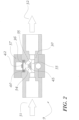
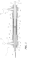
- the device 1 shown according to the invention which is suitable for carrying out the method of the invention, comprises a carrier 19 ("chuck") on which a semiconductor wafer 8 is placed.
- the carrier 19 can be designed in any desired manner and can be coupled to a drive (not shown) that causes the carrier 19 to rotate (arrow 20).
- the carrier 19 is assigned a device for applying a treatment medium, in the example a treatment liquid, which comprises a nozzle 11 that is rigidly connected to actuators 12 via a device 13.
- the actuators 12 allow the nozzle 11 of the application device to be moved via the device 13 relative to the surface of the object to be treated, in the exemplary embodiment a semiconductor wafer 8. Movement possibilities in direction X and direction Y are in Fig. 1 symbolized by arrows 5 and 6.
- Treatment fluid an etching medium when etching semiconductor wafers, is supplied to the nozzle 11 via a line 17.
- a device 4 for flow rate regulation Associated with the line 17 are a device 4 for flow rate regulation, a cooling device 3, and a device 2 for heating the fluid.
- the current position of the nozzle 11 and thus the location 7 of the liquid application are detected by incremental encoders 14 assigned to the actuators 12.
- the incremental encoders 14 transmit data concerning the current position of the application nozzle 11 relative to the surface of the wafer 8 to a control loop 10.
- a temperature sensor 9 is assigned to the line 17 for supplying treatment fluid directly upstream of the nozzle 11. This sensor transmits data concerning the fluid temperature it detects to the control circuit 10.
- the temperature parameters 16 transmitted to the control circuit 10 by the temperature sensor 9 and the position parameters 15 transmitted by the incremental encoders 14 are transmitted by the control circuit 10 as a control algorithm to the flow rate control devices 4, the cooling device 3, and the heating device 2 assigned to the line 17.
- the Fig. 1 The device 1 shown for temperature and/or flow manipulation of the liquid supplied from the nozzle 11 operates depending on the position of the nozzle 11 of the application device relative to the object to be treated, in the example the semiconductor wafer 8.
- an improvement in the Surface regularity is achieved during cleaning and during wet chemical and temperature-dependent etching, for example of wafer surfaces.
- a device is used as the heating device 2 which operates on an induction basis and heats the liquid flowing through the device 2 by convection.
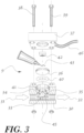
- a temperature sensor 9 which is particularly suitable for use with the device according to the invention for carrying out the method according to the invention for detecting the temperature of the treatment liquid applied to the object is described below with reference to Fig. 2 and 3 explained.
- the temperature sensor 9 shown allows for rapid detection of the temperature of media, wherein the media can be, in particular, chemically highly reactive gases, chemically highly reactive liquids, or chemically highly reactive flowing materials.
- the temperature sensor 9 is constructed such that the media flow entering its body 30 (arrow 31) is divided into two partial flows by a body 45 provided in the flow path.
- One partial flow flows through a substantially straight channel 33, and a second partial flow through an angled channel comprising two sections 34 and 35.
- the partial flow flowing through the channel sections 34 and 35 encounters a disk-shaped body 36 at an acute angle, for example, of 45°, and then flows out of the body 30 of the temperature sensor 9 through section 35 (arrow 32).
- the division into the partial flows results in a reduction in pressure in the area of the inlet to the temperature sensor 9.
- the disc-shaped body 36 is supported by the upper part 37 of the Temperature sensor 9 is pressed by screws 38 and 39 via a seal 40 onto a sealing surface 41 of the body 30 of the temperature sensor 9, resulting in a hermetically sealed system.
- the parts of the temperature sensor 9 that come into contact with the medium are preferably made of chemically resistant materials, for example the disk-shaped body 36 preferably being made of (polycrystalline) diamond, glassy carbon, sapphire or silicon carbide, optionally with CVD coating (chemical vapor deposition), the seal 40 preferably being made of perfluoro rubber (FFKM), and the body 30 of the temperature sensor 9 preferably being made of polytetrafluoroethylene (PTFE).
- the disk-shaped body 36 preferably being made of (polycrystalline) diamond, glassy carbon, sapphire or silicon carbide, optionally with CVD coating (chemical vapor deposition)
- the seal 40 preferably being made of perfluoro rubber (FFKM)
- the body 30 of the temperature sensor 9 preferably being made of polytetrafluoroethylene (PTFE).
- FFKM perfluoro rubber
- the temperature is detected in the temperature sensor 9 via a temperature sensor 42, which is, for example, a platinum thin-film measuring resistor.
- the temperature sensor 42 is preferably bonded to the disc-shaped body 36 using a thermally conductive adhesive 43 (two-component epoxy resin), so that good heat transfer is ensured.
- a line 46 leads from the temperature sensor 42, which transmits the data 16 detected by the temperature sensor 42 via the Fig. 1 shown line to control circuit 10.
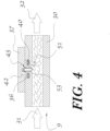
- FIG. 4 Another embodiment of a temperature sensor 9 is shown in Fig. 4 shown and is described below.
- the temperature sensor 9 can also be configured to be multiple, retentive.
- several temperature sensors 42 are glued to the disk 36 of the temperature sensor 9, whose temperature signals are compared using a monitoring program (software algorithm) to identify any temperature deviations due to aging, whereby these temperature differences should not exceed a certain difference. Exceeding the minimum temperature difference is indicated by a monitoring system with a signal. A change in the temperature difference can be indicated visually or acoustically. If several temperature sensors 42 are arranged on the disk 36, a multi-pole cable 46 is used to transmit the data recorded by the temperature sensors 42.
- the device 2 shown for heating a liquid or gaseous flowing medium has a hollow cylindrical heating element 60, around which the medium flows on its inside and outside, flowing in (arrow 63) and out (arrow 64) via connections 61, 62.
- the heating element 60 which consists, for example, of glassy carbon, is heated by alternating magnetic fields, particularly on its outside ("skin effect").
- the frequency of the magnetic field can range, for example, from 100 kHz to 1 MHz.
- the magnetic field is generated by a coil 65.
- the coil 65 is separated by a hose 66 from the heating element 60 and separated from the flowing medium.
- the energy is thus transferred without contact, which is a considerable advantage over conventional heating elements, which require electrical contact and must therefore be sealed from the medium to be treated.
- the interior space 67 is hermetically separated from the reactor chamber 69 by an inner tube 68 and via a sealing system with body 70, seal 71, clamping ring 72 and pressed part 73.
- the pressed part 73 serves to insert measuring sensors 74 (PT 100, PT 1000) and safety sensors 75 (e.g. TCO Thermal Cut Off), since the final magnetic energy in the axial center is minimal, meaning that the sensors can be damaged by strong electromagnetic fields and offer good access for better monitoring of the heating element. This is advantageous for safety-relevant operation.
- Sensors 74 and 75 are preferably arranged centrally and embedded in heat-conducting material 76, with cables 77 extending from sensors 74 and 75.
- An expanded outer tube 20 is pressed onto body 70 by means of a screw connection 78 and forms a hermetically sealed area from the reactor chamber 69 to the outside.
- the device 2 is mirror-symmetrical with respect to its center plane, thus the same applies to the outlet 62 as to the inlet 61.
- Outlet 62 and inlet 61 can also be provided with a screw-in fitting.
- a spacer ring 79 ( Fig. 10 and 11 ). A particular advantage is the short distance, as this results in rapid heat transfer from the heating element 60 to the medium flowing through the device 2.
- the inflowing medium is divided into an outer 80 and an inner flow area 81, so that the heating element 60 is completely surrounded by flow.
- the device 2 is designed so that all components are made of materials with low thermal inertia.
- Fig. 8 The device 2 is shown, wherein the coil 65, which preferably consists of a soft copper tube, is shown partially sectioned in an oblique view. Shown in Fig. 8 also the inlet 82 for a cooling liquid and the outlet 83 for a cooling liquid with which the coil 65 is cooled.
- the coil 65 which preferably consists of a soft copper tube
- the described structure of the device 2 also offers the possibility of flushing away or blowing out corrosive gases (e.g. hydrogen fluoride) occurring in the interior, for example by diffusion, by means of nitrogen, which enters via a flushing inlet 84 and exits again through the flushing outlet 85.
- corrosive gases e.g. hydrogen fluoride
- a device 3 for cooling is described below with reference to Fig. 9 explains:
- the Fig. 9 The device 3 shown for cooling liquid media has two plates 90 arranged one above the other and aligned parallel to each other.
- the space between the plates 90 is sealed by an edge seal 91, which seal 91 keeps the plates 90 spaced apart.
- the spacing of the plates 2 from one another is advantageously selected to enable good heat transfer to the medium to be cooled, which is supported by achieving turbulent flow.
- the plates 90 can be made of sapphire, diamond, glassy carbon, or silicon carbide, optionally with a silicon carbide layer (SiC) deposited thereon.
- the plates 2 and 3 are held between an upper part 92 and a lower part 93 of the device 3, which are held together by screws 94.
- a piece of pipe 95 is inserted into a The opening in the upper plate 92 is screwed into the hole 96 in the upper plate 90 and is sealed from the plate 90 by an annular seal (e.g., an O-ring).
- the pipe section 95 serves as an inlet for the medium to be cooled (arrow 97).
- a pipe section 95 is also screwed into the lower plate 2, which communicates with an opening 96 in the lower plate and is sealed from the plate 90 by an annular seal (e.g., an O-ring).
- the medium can exit the device 3 through the pipe section 95 after it has flowed through the space between the plates 90 (arrow 98).
- Peltier elements 100 are assigned to both sides of the plates in such a way that heat extracted from the medium is dissipated via the Peltier elements to a heat sink 101 arranged on the top and bottom.
- the cooling elements 101 each have an inlet 102 and an outlet 103 so that a cooling medium can flow through them.
- Fig. 9 It is also indicated that the Peltier elements are brought into good thermal conduction connection with the heat sinks 101 by means of thermally conductive adhesive 104.
- the Fig. 9 The device shown can, after reversing the polarity of the Peltier elements 100, in principle also be used to heat a medium flowing through the device 3.
- the device 4 for regulating the flow of a medium comprises a diaphragm 110, which has a needle-shaped, tapered projection on one side, the distance of which from the valve seat 111, which is integrally connected to a body 112, can be varied by means of an adjusting device 113, 114.
- the adjusting device preferably comprises a stepper motor 113, whose spindle 114 represents a drive for the diaphragm 110.
- the spindle 114 does not rotate and is by means of a rotating sleeve built into the motor 113, it is moved only linearly.
- Medium is introduced into the inlet 115 and exits via the outlet 116.
- the bodies 117 and 118 serve only to position the stepper motor 113 and to seal the diaphragm 110, for which screw connections (not shown) are provided.
- a sensor 119 detects the distance of the diaphragm 110 or its clearance from the valve seat 111, which data is fed to the control system.
- the schematically illustrated embodiment of the flow manipulation device 4 determines the flow rate using a flow sensor 121 (for example, an ultrasonic flow sensor).
- the values thus detected are fed via a signal line 112 to a controller 123, which, via a further control line 124, operates the actuator 113, 114 (stepper motor) of the flow controller 129, which in turn transmits its current position to the controller via a position control via a control line 125.
- the flow of the medium via inlet 127 and through outlet 128 can be specified externally via a main control line 126.
- a cooling device is advantageously used that compensates for local temperature differences, taking into account the current settings of the system and the medium to be treated to avoid any interference factors, heat sinks, etc.
- the modified embodiment of a device 130 according to the invention shown in FIG. 1 is an extension of the device 1 according to Fig. 1 .
- the device 130 also comprises devices 134 for regulating the temperature and devices 4 for regulating the flow rate of the treatment medium applied to the wafer 8 through the nozzle 11 (treatment fluid).
- the device 130 according to Fig. 12 Devices with which the concentration of the treatment medium (etching liquid) can be changed depending on the position of the nozzle 11 and thus the location 7 at which the treatment medium is applied to the wafer 8.
- the device provided for this purpose comprises a sensor 133 that detects the concentration of the treatment medium.
- the concentration sensor 133 is a common pH meter or a spectrometer with which the concentration of the treatment fluid used can be determined.
- the device 130 operates as follows when adjusting the concentration depending on the nozzle 11:
- the components of the treatment medium are supplied via lines 137, and the defined concentration and temperature values in medium sources 136 are transmitted via a control line 138 to the control/regulation unit 131.
- a software algorithm converts the temperature values supplied via lines 138, the concentration values supplied via line 140, and the temperature values detected by the temperature sensor 9 into control signals. These control signals are transmitted via control lines 139 to the components 134 for regulating the temperature 134 and the device 4 for regulating the flow rate.
- the media streams are fed to a mixing device 132, which is designed in particular as a static mixer, and mixed with one another. When using a static mixer, rapid mixing can be achieved to achieve the desired temperature and/or concentration at the specified quantity.
- the points 135 drawn next to the flow rate controllers 4, the temperature controllers 134 and the media sources 136 indicate that more than two of these components can be provided.
- Fig. 13 Various combination options of heating devices 2 and cooling devices 3 are indicated. Further possibilities of combining the devices in Fig. 13 In the variants shown, the devices 134 for adjusting the temperature by heating and cooling the medium are conceivable, whereby the variant without a device for regulating the temperature 134 is also indicated at 141. If this variant, which is indicated at 141, is implemented, the temperature can be adjusted analogously to the adjustment of the concentration via flow controllers, without separate devices for heating and cooling, if the temperatures in the media sources 136 of the medium streams 137 are sufficiently different.
Landscapes
- Engineering & Computer Science (AREA)
- Computer Hardware Design (AREA)
- Physics & Mathematics (AREA)
- Condensed Matter Physics & Semiconductors (AREA)
- General Physics & Mathematics (AREA)
- Manufacturing & Machinery (AREA)
- Microelectronics & Electronic Packaging (AREA)
- Power Engineering (AREA)
- Robotics (AREA)
- Chemical & Material Sciences (AREA)
- Chemical Kinetics & Catalysis (AREA)
- General Chemical & Material Sciences (AREA)
- Weting (AREA)
- Cleaning Or Drying Semiconductors (AREA)
Applications Claiming Priority (2)
| Application Number | Priority Date | Filing Date | Title |
|---|---|---|---|
| ATA946/2013A AT515147B1 (de) | 2013-12-09 | 2013-12-09 | Verfahren und Vorrichtung zum Behandeln von Gegenständen mit einer Flüssigkeit |
| PCT/AT2014/000209 WO2015085334A1 (de) | 2013-12-09 | 2014-11-26 | Verfahren und vorrichtung zum behandeln von gegenständen mit einer flüssigkeit |
Publications (2)
| Publication Number | Publication Date |
|---|---|
| EP3080837A1 EP3080837A1 (de) | 2016-10-19 |
| EP3080837B1 true EP3080837B1 (de) | 2025-06-11 |
Family
ID=52394800
Family Applications (1)
| Application Number | Title | Priority Date | Filing Date |
|---|---|---|---|
| EP14830366.2A Active EP3080837B1 (de) | 2013-12-09 | 2014-11-26 | Verfahren und vorrichtung zum behandeln von gegenständen mit einem medium, insbesondere einer flüssigkeit |
Country Status (5)
| Country | Link |
|---|---|
| US (1) | US20160307770A1 (enExample) |
| EP (1) | EP3080837B1 (enExample) |
| JP (1) | JP6195673B2 (enExample) |
| AT (1) | AT515147B1 (enExample) |
| WO (1) | WO2015085334A1 (enExample) |
Families Citing this family (4)
| Publication number | Priority date | Publication date | Assignee | Title |
|---|---|---|---|---|
| US11581187B2 (en) * | 2018-12-20 | 2023-02-14 | Xia Tai Xin Semiconductor (Qing Dao) Ltd. | Method of heating SOC film on wafer by electromagnetic wave generator and heating apparatus using the same |
| WO2021061836A1 (en) * | 2019-09-23 | 2021-04-01 | Baldwin Technology Company, Inc. | System and method of sensing and processing multivariate printing process data |
| AT16977U3 (de) | 2020-02-20 | 2021-03-15 | 4Tex Gmbh | Verfahren zum Behandeln von Substraten mit Chemikalien |
| CN113878403B (zh) * | 2021-10-13 | 2024-10-29 | 洛阳开远智能精机有限公司 | 一种在线工件检测系统及工件检测方法 |
Family Cites Families (19)
| Publication number | Priority date | Publication date | Assignee | Title |
|---|---|---|---|---|
| US3707979A (en) * | 1969-02-28 | 1973-01-02 | Honeywell Inc | Cooled temperature sensitive oscillator |
| US5478435A (en) * | 1994-12-16 | 1995-12-26 | National Semiconductor Corp. | Point of use slurry dispensing system |
| TW346649B (en) * | 1996-09-24 | 1998-12-01 | Tokyo Electron Co Ltd | Method for wet etching a film |
| JPH11283950A (ja) * | 1998-03-30 | 1999-10-15 | Ebara Corp | 基板洗浄装置 |
| KR100265286B1 (ko) * | 1998-04-20 | 2000-10-02 | 윤종용 | 반도체장치 제조용 케미컬 순환공급장치 및 이의 구동방법 |
| US5965813A (en) * | 1998-07-23 | 1999-10-12 | Industry Technology Research Institute | Integrated flow sensor |
| JP2000265945A (ja) * | 1998-11-10 | 2000-09-26 | Uct Kk | 薬液供給ポンプ、薬液供給装置、薬液供給システム、基板洗浄装置、薬液供給方法、及び基板洗浄方法 |
| US6333275B1 (en) * | 1999-10-01 | 2001-12-25 | Novellus Systems, Inc. | Etchant mixing system for edge bevel removal of copper from silicon wafers |
| US6376013B1 (en) * | 1999-10-06 | 2002-04-23 | Advanced Micro Devices, Inc. | Multiple nozzles for dispensing resist |
| KR20010039993A (ko) * | 1999-10-06 | 2001-05-15 | 오카무라 가네오 | 유량 및 유속 측정장치 |
| DE60120339T2 (de) * | 2001-01-05 | 2007-06-06 | NGK Spark Plug Co., Ltd., Nagoya | Gasdurchflussmessvorrichtung |
| US6674054B2 (en) * | 2001-04-26 | 2004-01-06 | Phifer-Smith Corporation | Method and apparatus for heating a gas-solvent solution |
| US20080044939A1 (en) * | 2002-01-24 | 2008-02-21 | Nassiopoulou Androula G | Low power silicon thermal sensors and microfluidic devices based on the use of porous sealed air cavity technology or microchannel technology |
| US7300598B2 (en) * | 2003-03-31 | 2007-11-27 | Tokyo Electron Limited | Substrate processing method and apparatus |
| KR100708037B1 (ko) * | 2003-12-24 | 2007-04-16 | 마츠시타 덴끼 산교 가부시키가이샤 | 유체공급노즐, 기판처리장치 및 기판처리방법 |
| US20060084260A1 (en) * | 2004-09-07 | 2006-04-20 | Boyers David G | Copper processing using an ozone-solvent solution |
| JP4781834B2 (ja) * | 2006-02-07 | 2011-09-28 | 大日本スクリーン製造株式会社 | 現像装置および現像方法 |
| DE102009060931A1 (de) * | 2009-12-23 | 2011-06-30 | Gebr. Schmid GmbH & Co., 72250 | Verfahren und Vorrichtung zur Behandlung von Siliziumsubstraten |
| US8932962B2 (en) * | 2012-04-09 | 2015-01-13 | Taiwan Semiconductor Manufacturing Co., Ltd. | Chemical dispensing system and method |
-
2013
- 2013-12-09 AT ATA946/2013A patent/AT515147B1/de active
-
2014
- 2014-11-26 EP EP14830366.2A patent/EP3080837B1/de active Active
- 2014-11-26 JP JP2016539041A patent/JP6195673B2/ja active Active
- 2014-11-26 US US15/103,025 patent/US20160307770A1/en not_active Abandoned
- 2014-11-26 WO PCT/AT2014/000209 patent/WO2015085334A1/de not_active Ceased
Also Published As
| Publication number | Publication date |
|---|---|
| US20160307770A1 (en) | 2016-10-20 |
| JP2017500742A (ja) | 2017-01-05 |
| AT515147B1 (de) | 2016-10-15 |
| AT515147A1 (de) | 2015-06-15 |
| JP6195673B2 (ja) | 2017-09-13 |
| WO2015085334A1 (de) | 2015-06-18 |
| EP3080837A1 (de) | 2016-10-19 |
Similar Documents
| Publication | Publication Date | Title |
|---|---|---|
| EP3080837B1 (de) | Verfahren und vorrichtung zum behandeln von gegenständen mit einem medium, insbesondere einer flüssigkeit | |
| DE3301288C2 (enExample) | ||
| DE69629980T2 (de) | Methode mit Temperaturreglung zum Abscheiden eines Werkstoffes | |
| DE102006045028B4 (de) | Konstanttemperatur-Flüssigkeitszirkuliervorrichtung und Verfahren zur Steuerung der Temperatur in der Vorrichtung | |
| DE102016103270B3 (de) | Vorrichtung und Verfahren zur Halterung, Rotation sowie Heizung und/oder Kühlung eines Substrats | |
| DE102012217601B4 (de) | NMR-Messanordnung mit Temperiereinrichtung für ein Probenröhrchen | |
| DE102004057215A1 (de) | Verfahren und Vorrichtung zum Testen von Halbleiterwafern mittels einer Sondenkarte | |
| WO2018166955A1 (de) | Verfahren und vorrichtung zur thermischen behandlung eines substrates | |
| AT524363B1 (de) | Messgerät mit elektrothermischem Wandler zum Einstellen eines thermischen Widerstandes, und Betriebsverfahren | |
| DE2255736B2 (de) | Elektrische Heizvorrichtung | |
| WO2016162088A1 (de) | Substrathalter und verfahren zum bonden zweier substrate | |
| DE60126589T2 (de) | Thermisches kontrollsystem für substrate | |
| JP4741562B2 (ja) | 基板熱管理の方法 | |
| WO2017137420A2 (de) | Sintervorrichtung | |
| EP2469577B1 (de) | Vorrichtung zur Kühlung von Proben während einer Ionenstrahlpräparation | |
| DE10119041A1 (de) | Verfahren zum Kühlen einer Induktionsspule | |
| EP1590510B1 (de) | Vorrichtung zur herstellung elektrisch leitfähiger durchgänge in einem halbleiterwafer mittels thermomigration | |
| WO2010003661A1 (de) | Teststand mit steuerbaren oder regelbaren restriktoren | |
| DE4018094C2 (enExample) | ||
| DE102008032098A1 (de) | Teststand mit steuerbaren oder regelbaren Restriktoren | |
| DE9401808U1 (de) | Vorrichtung zum Regeln der Temperatur von Lasergas, insbesondere eines Excimerlasers | |
| DE102004022453B4 (de) | Ventilsteuereinrichtung mit Leckratenberücksichtigung | |
| DE102008032097A1 (de) | Teststand mit Gruppen von Restriktoren | |
| DE1912604B2 (de) | Probenkopfvorrichtung fuer die kernresonanzspektroskopie | |
| DE10245043B3 (de) | Vorrichtung und Verfahren zur Verdunstung von Narkosemittel |
Legal Events
| Date | Code | Title | Description |
|---|---|---|---|
| PUAI | Public reference made under article 153(3) epc to a published international application that has entered the european phase |
Free format text: ORIGINAL CODE: 0009012 |
|
| 17P | Request for examination filed |
Effective date: 20160602 |
|
| AK | Designated contracting states |
Kind code of ref document: A1 Designated state(s): AL AT BE BG CH CY CZ DE DK EE ES FI FR GB GR HR HU IE IS IT LI LT LU LV MC MK MT NL NO PL PT RO RS SE SI SK SM TR |
|
| AX | Request for extension of the european patent |
Extension state: BA ME |
|
| RIN1 | Information on inventor provided before grant (corrected) |
Inventor name: LINDER, MANUEL Inventor name: HOFER-MOSER, JOERG |
|
| DAX | Request for extension of the european patent (deleted) | ||
| RAP1 | Party data changed (applicant data changed or rights of an application transferred) |
Owner name: SMOLINER, KLAUS Owner name: HOFER-MOSER, JOERG |
|
| RIN1 | Information on inventor provided before grant (corrected) |
Inventor name: LINDER, MANUEL Inventor name: HOFER-MOSER, JOERG Inventor name: SMOLINER, KLAUS |
|
| RAP1 | Party data changed (applicant data changed or rights of an application transferred) |
Owner name: 4TEX GMBH |
|
| STAA | Information on the status of an ep patent application or granted ep patent |
Free format text: STATUS: EXAMINATION IS IN PROGRESS |
|
| 17Q | First examination report despatched |
Effective date: 20210518 |
|
| GRAP | Despatch of communication of intention to grant a patent |
Free format text: ORIGINAL CODE: EPIDOSNIGR1 |
|
| STAA | Information on the status of an ep patent application or granted ep patent |
Free format text: STATUS: GRANT OF PATENT IS INTENDED |
|
| INTG | Intention to grant announced |
Effective date: 20240809 |
|
| GRAJ | Information related to disapproval of communication of intention to grant by the applicant or resumption of examination proceedings by the epo deleted |
Free format text: ORIGINAL CODE: EPIDOSDIGR1 |
|
| STAA | Information on the status of an ep patent application or granted ep patent |
Free format text: STATUS: EXAMINATION IS IN PROGRESS |
|
| GRAP | Despatch of communication of intention to grant a patent |
Free format text: ORIGINAL CODE: EPIDOSNIGR1 |
|
| STAA | Information on the status of an ep patent application or granted ep patent |
Free format text: STATUS: GRANT OF PATENT IS INTENDED |
|
| INTC | Intention to grant announced (deleted) | ||
| INTG | Intention to grant announced |
Effective date: 20250102 |
|
| RIN1 | Information on inventor provided before grant (corrected) |
Inventor name: SMOLINER, KLAUS Inventor name: LINDER, MANUEL Inventor name: HOFER-MOSER, JOERG |
|
| GRAS | Grant fee paid |
Free format text: ORIGINAL CODE: EPIDOSNIGR3 |
|
| GRAA | (expected) grant |
Free format text: ORIGINAL CODE: 0009210 |
|
| STAA | Information on the status of an ep patent application or granted ep patent |
Free format text: STATUS: THE PATENT HAS BEEN GRANTED |
|
| AK | Designated contracting states |
Kind code of ref document: B1 Designated state(s): AL AT BE BG CH CY CZ DE DK EE ES FI FR GB GR HR HU IE IS IT LI LT LU LV MC MK MT NL NO PL PT RO RS SE SI SK SM TR |
|
| REG | Reference to a national code |
Ref country code: GB Ref legal event code: FG4D Free format text: NOT ENGLISH |
|
| REG | Reference to a national code |
Ref country code: CH Ref legal event code: EP |
|
| REG | Reference to a national code |
Ref country code: IE Ref legal event code: FG4D Free format text: LANGUAGE OF EP DOCUMENT: GERMAN |
|
| REG | Reference to a national code |
Ref country code: DE Ref legal event code: R096 Ref document number: 502014016935 Country of ref document: DE |
|
| P01 | Opt-out of the competence of the unified patent court (upc) registered |
Free format text: CASE NUMBER: APP_27393/2025 Effective date: 20250610 |
|
| PG25 | Lapsed in a contracting state [announced via postgrant information from national office to epo] |
Ref country code: ES Free format text: LAPSE BECAUSE OF FAILURE TO SUBMIT A TRANSLATION OF THE DESCRIPTION OR TO PAY THE FEE WITHIN THE PRESCRIBED TIME-LIMIT Effective date: 20250611 Ref country code: FI Free format text: LAPSE BECAUSE OF FAILURE TO SUBMIT A TRANSLATION OF THE DESCRIPTION OR TO PAY THE FEE WITHIN THE PRESCRIBED TIME-LIMIT Effective date: 20250611 |
|
| REG | Reference to a national code |
Ref country code: LT Ref legal event code: MG9D |
|
| PG25 | Lapsed in a contracting state [announced via postgrant information from national office to epo] |
Ref country code: GR Free format text: LAPSE BECAUSE OF FAILURE TO SUBMIT A TRANSLATION OF THE DESCRIPTION OR TO PAY THE FEE WITHIN THE PRESCRIBED TIME-LIMIT Effective date: 20250912 Ref country code: NO Free format text: LAPSE BECAUSE OF FAILURE TO SUBMIT A TRANSLATION OF THE DESCRIPTION OR TO PAY THE FEE WITHIN THE PRESCRIBED TIME-LIMIT Effective date: 20250911 |
|
| REG | Reference to a national code |
Ref country code: NL Ref legal event code: MP Effective date: 20250611 |
|
| PG25 | Lapsed in a contracting state [announced via postgrant information from national office to epo] |
Ref country code: BG Free format text: LAPSE BECAUSE OF FAILURE TO SUBMIT A TRANSLATION OF THE DESCRIPTION OR TO PAY THE FEE WITHIN THE PRESCRIBED TIME-LIMIT Effective date: 20250611 |
|
| PG25 | Lapsed in a contracting state [announced via postgrant information from national office to epo] |
Ref country code: HR Free format text: LAPSE BECAUSE OF FAILURE TO SUBMIT A TRANSLATION OF THE DESCRIPTION OR TO PAY THE FEE WITHIN THE PRESCRIBED TIME-LIMIT Effective date: 20250611 |
|
| PG25 | Lapsed in a contracting state [announced via postgrant information from national office to epo] |
Ref country code: RS Free format text: LAPSE BECAUSE OF FAILURE TO SUBMIT A TRANSLATION OF THE DESCRIPTION OR TO PAY THE FEE WITHIN THE PRESCRIBED TIME-LIMIT Effective date: 20250911 |
|
| PG25 | Lapsed in a contracting state [announced via postgrant information from national office to epo] |
Ref country code: LV Free format text: LAPSE BECAUSE OF FAILURE TO SUBMIT A TRANSLATION OF THE DESCRIPTION OR TO PAY THE FEE WITHIN THE PRESCRIBED TIME-LIMIT Effective date: 20250611 |
|
| PG25 | Lapsed in a contracting state [announced via postgrant information from national office to epo] |
Ref country code: NL Free format text: LAPSE BECAUSE OF FAILURE TO SUBMIT A TRANSLATION OF THE DESCRIPTION OR TO PAY THE FEE WITHIN THE PRESCRIBED TIME-LIMIT Effective date: 20250611 |
|
| REG | Reference to a national code |
Ref country code: DE Ref legal event code: R079 Ref document number: 502014016935 Country of ref document: DE Free format text: PREVIOUS MAIN CLASS: H01L0021670000 Ipc: H10P0072000000 |
|
| PG25 | Lapsed in a contracting state [announced via postgrant information from national office to epo] |
Ref country code: PT Free format text: LAPSE BECAUSE OF FAILURE TO SUBMIT A TRANSLATION OF THE DESCRIPTION OR TO PAY THE FEE WITHIN THE PRESCRIBED TIME-LIMIT Effective date: 20251013 |
|
| PG25 | Lapsed in a contracting state [announced via postgrant information from national office to epo] |
Ref country code: IS Free format text: LAPSE BECAUSE OF FAILURE TO SUBMIT A TRANSLATION OF THE DESCRIPTION OR TO PAY THE FEE WITHIN THE PRESCRIBED TIME-LIMIT Effective date: 20251011 |