EP3078056B1 - Electroactive device and a method of fabricating the same - Google Patents
Electroactive device and a method of fabricating the same Download PDFInfo
- Publication number
- EP3078056B1 EP3078056B1 EP14868114.1A EP14868114A EP3078056B1 EP 3078056 B1 EP3078056 B1 EP 3078056B1 EP 14868114 A EP14868114 A EP 14868114A EP 3078056 B1 EP3078056 B1 EP 3078056B1
- Authority
- EP
- European Patent Office
- Prior art keywords
- layers
- substrate
- electroactive
- layer
- electrochromic
- Prior art date
- Legal status (The legal status is an assumption and is not a legal conclusion. Google has not performed a legal analysis and makes no representation as to the accuracy of the status listed.)
- Active
Links
Images


Classifications
-
- G—PHYSICS
- G02—OPTICS
- G02F—OPTICAL DEVICES OR ARRANGEMENTS FOR THE CONTROL OF LIGHT BY MODIFICATION OF THE OPTICAL PROPERTIES OF THE MEDIA OF THE ELEMENTS INVOLVED THEREIN; NON-LINEAR OPTICS; FREQUENCY-CHANGING OF LIGHT; OPTICAL LOGIC ELEMENTS; OPTICAL ANALOGUE/DIGITAL CONVERTERS
- G02F1/00—Devices or arrangements for the control of the intensity, colour, phase, polarisation or direction of light arriving from an independent light source, e.g. switching, gating or modulating; Non-linear optics
- G02F1/01—Devices or arrangements for the control of the intensity, colour, phase, polarisation or direction of light arriving from an independent light source, e.g. switching, gating or modulating; Non-linear optics for the control of the intensity, phase, polarisation or colour
- G02F1/15—Devices or arrangements for the control of the intensity, colour, phase, polarisation or direction of light arriving from an independent light source, e.g. switching, gating or modulating; Non-linear optics for the control of the intensity, phase, polarisation or colour based on an electrochromic effect
- G02F1/153—Constructional details
- G02F1/1533—Constructional details structural features not otherwise provided for
-
- B—PERFORMING OPERATIONS; TRANSPORTING
- B23—MACHINE TOOLS; METAL-WORKING NOT OTHERWISE PROVIDED FOR
- B23K—SOLDERING OR UNSOLDERING; WELDING; CLADDING OR PLATING BY SOLDERING OR WELDING; CUTTING BY APPLYING HEAT LOCALLY, e.g. FLAME CUTTING; WORKING BY LASER BEAM
- B23K26/00—Working by laser beam, e.g. welding, cutting or boring
- B23K26/02—Positioning or observing the workpiece, e.g. with respect to the point of impact; Aligning, aiming or focusing the laser beam
- B23K26/06—Shaping the laser beam, e.g. by masks or multi-focusing
- B23K26/062—Shaping the laser beam, e.g. by masks or multi-focusing by direct control of the laser beam
- B23K26/0626—Energy control of the laser beam
-
- B—PERFORMING OPERATIONS; TRANSPORTING
- B23—MACHINE TOOLS; METAL-WORKING NOT OTHERWISE PROVIDED FOR
- B23K—SOLDERING OR UNSOLDERING; WELDING; CLADDING OR PLATING BY SOLDERING OR WELDING; CUTTING BY APPLYING HEAT LOCALLY, e.g. FLAME CUTTING; WORKING BY LASER BEAM
- B23K26/00—Working by laser beam, e.g. welding, cutting or boring
- B23K26/36—Removing material
- B23K26/362—Laser etching
- B23K26/364—Laser etching for making a groove or trench, e.g. for scribing a break initiation groove
-
- C—CHEMISTRY; METALLURGY
- C23—COATING METALLIC MATERIAL; COATING MATERIAL WITH METALLIC MATERIAL; CHEMICAL SURFACE TREATMENT; DIFFUSION TREATMENT OF METALLIC MATERIAL; COATING BY VACUUM EVAPORATION, BY SPUTTERING, BY ION IMPLANTATION OR BY CHEMICAL VAPOUR DEPOSITION, IN GENERAL; INHIBITING CORROSION OF METALLIC MATERIAL OR INCRUSTATION IN GENERAL
- C23C—COATING METALLIC MATERIAL; COATING MATERIAL WITH METALLIC MATERIAL; SURFACE TREATMENT OF METALLIC MATERIAL BY DIFFUSION INTO THE SURFACE, BY CHEMICAL CONVERSION OR SUBSTITUTION; COATING BY VACUUM EVAPORATION, BY SPUTTERING, BY ION IMPLANTATION OR BY CHEMICAL VAPOUR DEPOSITION, IN GENERAL
- C23C14/00—Coating by vacuum evaporation, by sputtering or by ion implantation of the coating forming material
- C23C14/06—Coating by vacuum evaporation, by sputtering or by ion implantation of the coating forming material characterised by the coating material
- C23C14/08—Oxides
- C23C14/086—Oxides of zinc, germanium, cadmium, indium, tin, thallium or bismuth
-
- C—CHEMISTRY; METALLURGY
- C23—COATING METALLIC MATERIAL; COATING MATERIAL WITH METALLIC MATERIAL; CHEMICAL SURFACE TREATMENT; DIFFUSION TREATMENT OF METALLIC MATERIAL; COATING BY VACUUM EVAPORATION, BY SPUTTERING, BY ION IMPLANTATION OR BY CHEMICAL VAPOUR DEPOSITION, IN GENERAL; INHIBITING CORROSION OF METALLIC MATERIAL OR INCRUSTATION IN GENERAL
- C23C—COATING METALLIC MATERIAL; COATING MATERIAL WITH METALLIC MATERIAL; SURFACE TREATMENT OF METALLIC MATERIAL BY DIFFUSION INTO THE SURFACE, BY CHEMICAL CONVERSION OR SUBSTITUTION; COATING BY VACUUM EVAPORATION, BY SPUTTERING, BY ION IMPLANTATION OR BY CHEMICAL VAPOUR DEPOSITION, IN GENERAL
- C23C14/00—Coating by vacuum evaporation, by sputtering or by ion implantation of the coating forming material
- C23C14/22—Coating by vacuum evaporation, by sputtering or by ion implantation of the coating forming material characterised by the process of coating
- C23C14/34—Sputtering
-
- G—PHYSICS
- G02—OPTICS
- G02F—OPTICAL DEVICES OR ARRANGEMENTS FOR THE CONTROL OF LIGHT BY MODIFICATION OF THE OPTICAL PROPERTIES OF THE MEDIA OF THE ELEMENTS INVOLVED THEREIN; NON-LINEAR OPTICS; FREQUENCY-CHANGING OF LIGHT; OPTICAL LOGIC ELEMENTS; OPTICAL ANALOGUE/DIGITAL CONVERTERS
- G02F1/00—Devices or arrangements for the control of the intensity, colour, phase, polarisation or direction of light arriving from an independent light source, e.g. switching, gating or modulating; Non-linear optics
- G02F1/01—Devices or arrangements for the control of the intensity, colour, phase, polarisation or direction of light arriving from an independent light source, e.g. switching, gating or modulating; Non-linear optics for the control of the intensity, phase, polarisation or colour
- G02F1/15—Devices or arrangements for the control of the intensity, colour, phase, polarisation or direction of light arriving from an independent light source, e.g. switching, gating or modulating; Non-linear optics for the control of the intensity, phase, polarisation or colour based on an electrochromic effect
- G02F1/153—Constructional details
- G02F1/155—Electrodes
- G02F2001/1555—Counter electrode
-
- G—PHYSICS
- G02—OPTICS
- G02F—OPTICAL DEVICES OR ARRANGEMENTS FOR THE CONTROL OF LIGHT BY MODIFICATION OF THE OPTICAL PROPERTIES OF THE MEDIA OF THE ELEMENTS INVOLVED THEREIN; NON-LINEAR OPTICS; FREQUENCY-CHANGING OF LIGHT; OPTICAL LOGIC ELEMENTS; OPTICAL ANALOGUE/DIGITAL CONVERTERS
- G02F2201/00—Constructional arrangements not provided for in groups G02F1/00 - G02F7/00
- G02F2201/50—Protective arrangements
- G02F2201/503—Arrangements improving the resistance to shock
-
- Y—GENERAL TAGGING OF NEW TECHNOLOGICAL DEVELOPMENTS; GENERAL TAGGING OF CROSS-SECTIONAL TECHNOLOGIES SPANNING OVER SEVERAL SECTIONS OF THE IPC; TECHNICAL SUBJECTS COVERED BY FORMER USPC CROSS-REFERENCE ART COLLECTIONS [XRACs] AND DIGESTS
- Y10—TECHNICAL SUBJECTS COVERED BY FORMER USPC
- Y10T—TECHNICAL SUBJECTS COVERED BY FORMER US CLASSIFICATION
- Y10T29/00—Metal working
- Y10T29/49—Method of mechanical manufacture
- Y10T29/49002—Electrical device making
- Y10T29/49117—Conductor or circuit manufacturing
- Y10T29/49124—On flat or curved insulated base, e.g., printed circuit, etc.
- Y10T29/49155—Manufacturing circuit on or in base
- Y10T29/49156—Manufacturing circuit on or in base with selective destruction of conductive paths
Definitions
- the present disclosure relates to improvements in electroactive devices and more particularly relates to improvements in solid-state, inorganic thin film devices.
- Electrochromic materials and devices have been developed as an alternative to passive coating materials for light and heat management in building and vehicle windows.
- electroactive devices employ materials capable of reversibly altering their optical properties following electrochemical oxidation and reduction in response to an applied potential. The optical modulation is the result of the simultaneous insertion and extraction of electrons and charge compensating ions in the electrochemical material lattice.
- FIG. 1 illustrates a typical five layer solid-state electrochromic device in cross-section having the five following superimposed layers: an electrochromic electrode layer (“EC") 14 which produces a change in absorption or reflection upon oxidation or reduction; an ion conductor layer (“IC") 13 which functionally replaces an electrolyte, allowing the passage of ions while blocking electronic current; a counter electrode layer (“CE”) 12 which serves as a storage layer for ions when the device is in the bleached or clear state; and two transparent conductive layers (“TCLs”) 11 and 15 which serve to apply an electrical potential to the electrochromic device.
- EC electrochromic electrode layer
- IC ion conductor layer
- CE counter electrode layer
- TCLs transparent conductive layers
- FIG. 2 illustrates the electrochromic device of FIG. 1 , in cross-section, having power supplied from two conductive elements, such as busbars 18 and 19.
- the busbars are electrically isolated from one another. Conventionally, this is done by scribing the TCLs 11 and 15. As shown in FIG. 2 , the first (lower) TCL 15 is scribed at point PI, making the lower TCL 15 a discontinuous (i.e., physically separate) layer, and thereby preventing the busbars from shorting across the lower TCL 15.
- the width of the scribe at point P1 is typically on the order of 25 microns or wider, while the length varies based on the width of the particular device being formed.
- the second (upper) TCL 11 is scribed at point P3, making the upper TCL 11 also discontinuous, and thereby preventing the busbars from being shorted together across the upper TCL 11.
- the P3 scribe is typically on the order of 25 microns or wider, while the length varies based on the width the particular device being formed.
- the thickness of the ion conductor layer may result in a reduction of leakage current, but at the expense of degraded optical properties, increased layer deposition time and cost, and reduced switching rates.
- adding dielectric layers to the stack may reduce leakage current but at the cost of similar defects and possible yield reduction.
- the yield can be considered to be reduced every time a substrate or other workpiece is cycled between the deposition chamber and atmosphere, and vice versa. This is because dust and debris from the coating process - which are inevitably present in film deposition - are 'blown' around during purging, venting, and/or pumpdown, and can find its way onto the active layers, leading to defects in the film structure.
- all the layers could be deposited in one single continuous process step, i.e., one coating machine.
- depositing additional dielectric layers could require transporting the workpiece between coaters to deposit the additional layers and then transporting the workpiece back to resume fabrication of the above described EC stack.
- Such transportation which could involve the workpiece exiting and reentering the deposition system and/or additional handling of the workpiece, would significantly increase production time, increase the device's exposure to particles and other contaminants, and greatly increase the risk of damage (e.g., scratching, mishandling, etc.) of the device. Accordingly, it is desirable to reduce the amount of electronic leakage through an electrochromic device without resorting to a thick ion conductor layer or additional dielectric layers so as to avoid these compromises in performance.
- any electroactive device having one or more functional electroactive layers sandwiched between top and bottom conductive layers may present similar challenges if a conductive layer is scribed to prevent shorting across that conductive layer.
- an electroactive device e.g., an electroluminescent device having a Conductor/Insulator/ Phosphor/Insulator/Conductor structure, an organic light emitting diode (OLED) having a Conductor/Electron Transport Layer/Emitting Layer/Hole Transport Layer/Conductor structure, or photovoltaic device having a Conductor/Electron Donor/P-N Junction/Electron Acceptor/ Conductor structure, etc.
- OLED organic light emitting diode
- photovoltaic device having a Conductor/Electron Donor/P-N Junction/Electron Acceptor/ Conductor structure, etc.
- the electrochromic device it is desirable to reduce the amount of electronic leakage between the portions of the transparent conductive layers of the electrochromic device while maintaining as high a yield as possible (e.g., conducting as few scribing steps during the cutting process as possible). More generally, it is desirable to reduce the amount of electronic leakage between upper and lower (i.e., opposing) conductive layers in any electroactive device in which scribing performed during production of the device may lead to electronic leakage from delamination or melting of the scribed layers, and to still maintain as high a yield as possible during production
- JP 2004 198966 A discloses an electrochromic rear-view mirror wherein the lower electrode is laser scribed from the EC stack side of the substrate and remaining layers are deposited over the scribe.
- WO 2013/090209 A1 discloses an electrochromic device wherein an edge portion of the lower electrode is tapered using a laser for reducing heat damage in the scribe area and for improving the quality of subsequently deposited layers covering the edge and reducing mechanical stress in those layer.
- the pulse duration is between about 1 ps and about 50 ns.
- One aspect of the invention provides an electroactive device including a first conductive layer, a second conductive layer, and one or more electroactive layers sandwiched between the first and second conductive layers.
- the electroactive device is an electrochromic device.
- the one or more electroactive layers include a first electrode that includes one of an electrochromic electrode layer and a counter electrode layer, and a second electrode that includes the other of the electrochromic electrode layer and the counter electrode layer.
- the one or more electroactive layers of the electroactive device further include an ion-conductor layer for conducting ions between the first and second electrodes.
- One or more adjacent layers of the device include a physical separation between a first portion and a second portion of the one or more adjacent layers.
- the physical separation defines respectively tapered sidewalls of each of the first and second portions.
- the respective tapered sidewall has an incline of about 45 degrees or less relative to the plane of the substrate.
- the one or more adjacent layers are more than one adjacent layers.
- the remaining layers of the electroactive device are formed on the one or more adjacent layers over the physical separation.
- the one or more adjacent layers include one of the first and second conductive layers and one of the first and second electrodes, and the remaining layers of the electroactive device include the other of the first and second conductive layers, the other of the first and second electrodes and the ion-conductor layer.
- the one or more adjacent layers may be at least about twice as thick as the remaining layers of the electroactive (e.g., electrochromic, etc.) device that are between the scribed adjacent layers and the other of the first and second conductive layer (i.e., the conductive layer not scribed at PI, as defined below). In further examples, the one or more adjacent layers may be at least about three times as thick as the remaining layers of the electroactive (e.g., electrochromic, etc.) device that are between the scribed adjacent layers and the other of the first and second conductive layer (i.e., the conductive layer not scribed at PI, as defined below).
- one of the first and second electrodes may be formed directly above the conductive layer having the physical separation.
- the physical separation between the first and second portions may be filled at least partially by the above electrode.
- the conductive layer having the physical separation does not have melt spots along the tapered sidewalls. In some further examples, the conductive layer having the physical separation may directly touch the substrate without having delamination along the respective tapered sidewalls.
- each of the tapered sidewalls may have a substantially linear profile. In other examples, each of the tapered sidewalls may have a substantially Gaussian profile. The incline of each of the tapered sidewalls (i.e., with respect or relative to the substrate) is about 45 degrees or less relative to the plane of the substrate such that each sidewall does not exhibit shadowing.
- the electroactive device may further include a physical separation between the second portion and a third portion of the plurality of electroactive layers. That physical separation may define a respective tapered sidewall of each of the second and third portions.
- the electroactive device includes a first conductive layer, a second conductive layer, and one or more electroactive layers sandwiched between the first and second conductive layers.
- the electroactive device is an electrochromic device.
- the one or more electroactive layers comprise: a first electrode including one of an electrochromic electrode layer and a counter electrode layer; a second electrode including the other of the electrochromic electrode layer and the counter electrode layer; and an ion-conductor layer for conducting ions between the first and second electrodes.
- the method includes providing a substrate and forming one or more adjacent layers of the electroactive device on the surface of the substrate. The one or more adjacent layers are more than one adjacent layers.
- the one or more adjacent layers include one of the first and second conductive layers and one of the first and second electrodes.
- the method further includes positioning a scribing implement, such as a laser, towards the substrate.
- the scribing implement is positioned incident the side of the substrate having the one or more adjacent layers formed thereon (i.e., the film side).
- the laser may have a pulse width of about 100 picoseconds or shorter.
- the method further includes removing a portion of the one or more adjacent layers, thereby forming a physical separation between a first portion and a second portion of the one or more adjacent layers, the physical separation defining a respective tapered sidewall of each of the first and second portions, wherein the respective tapered sidewall has an incline of about 45 degrees or less relative to the plane of the substrate.
- the method further includes forming one or more of the remaining layers of the device over the physical separation of the one or more adjacent layers.
- the remaining layers include the other of the first and second conductive layers, the other of the first and second electrodes, and the ion-conductor layer.
- the electroactive device includes a first conductive layer, a second conductive layer, and one or more electroactive layers sandwiched between the first and second conductive layers.
- the electroactive device is an electrochromic device.
- the one or more electroactive layers include: a first electrode comprising one of an electrochromic electrode layer and a counter electrode layer; a second electrode comprising the other of the electrochromic electrode layer and the counter electrode layer; and an ion-conductor layer for conducting ions between the first and second electrodes.
- the method further includes providing a substrate and forming one or more adjacent layers of the electroactive device on the surface of the substrate. The one or more adjacent layers are more than one adjacent layers.
- the one or more adjacent layers include one of the first and second conductive layers and one of the first and second electrodes.
- the method further includes providing a laser with a pulse width of about 100 picoseconds or shorter.
- the method further includes removing a portion of the one or more adjacent layers from the substrate using the laser, thereby forming a physical separation between a first portion and a second portion of the one or more adjacent layers, the physical separation defining a respective tapered sidewall of each of the first and second portions, wherein the respective tapered sidewall has an incline of about 45 degrees or less relative to the plane of the substrate.
- the method further includes forming the remaining layers of the electroactive device over the one or more adjacent layers.
- the remaining layers include the other of the first and second conductive layers, the other of the first and second electrodes, and the ion-conductor layer.
- the pulse width of the laser may be even shorter than 100 picoseconds.
- the pulse width may be about 10 picoseconds or shorter.
- the pulse width of the laser may be about 6 picoseconds.
- the wavelength of the laser may be between about 340 nm and about 1070 nm. In further examples, the wavelength may be between about 515 nm and about 532 nm.
- an electrochromic device including a first conductive layer, a second conductive layer, and one or more electroactive layers sandwiched between the first and second conductive layers.
- the one or more electroactive layers include: a first electrode including one of an electrochromic electrode layer and a counter electrode layer; a second electrode including the other of the electrochromic electrode layer and the counter electrode layer; and an ion-conductor layer for conducting ions between the first and second electrodes.
- the system includes a housing for containing a substrate on which the electrochromic device is formed.
- the system includes a deposition system configured to deposit one or more layers of the electrochromic device onto the substrate.
- the system includes a laser mounted in the housing, the laser positioned to produce a beam on the surface of the substrate.
- the laser is configured for removing a portion of one or more adjacent layers of the electrochromic device from the substrate, thereby forming a physical separation between a first portion and a second portion of the one or more adjacent layers.
- the one or more adjacent layers are more than one adjacent layers, the one or more adjacent layers including one of the first and second conductive layers and one of the first and second electrodes.
- the physical separation defines a respective tapered sidewall of each of the first and second portions, wherein the respective tapered sidewall has an incline of about 45 degrees or less relative to the plane of the substrate.
- the laser (a) has a pulse width of 100 picoseconds or shorter and is positioned to produce a beam on the substrate or (b) is incident to the side of the substrate on which the electrochromic device is formed.
- the system further includes a positioning device for moving the beam relative the substrate, and a collection system for collecting particulate materials or vapors generated by focusing of the beam on the surface of the substrate.
- every layer of the electroactive device which is formed during the first stage of fabrication may be formed without removing the substrate from the housing.
- each of the above described steps, including the scribing step, may be performed in a single continuous vacuum step within the housing.
- the present disclosure provides an electroactive layer structure having a reduced amount of electronic leakage between the upper and lower conductive layers.
- This structure is to be obtainable by a production method that maintains as high a yield as possible.
- These objectives are implemented by providing a properly adjusted laser having a pulse width on the order of about 100 picoseconds or shorter.
- the pulse width may be about 50 picoseconds or shorter.
- the pulse width may be about 10 picoseconds or shorter.
- the pulse width may be about 6 picoseconds.
- scribing the lower layer or layers of the electroactive structure using a laser with a pulse width on the order of about 100 picoseconds or shorter optimizes the amount of spreading of heating across the layer structure during the scribing process.
- a pulse width of about 100 picoseconds or shorter has been found to be long enough to remove or ablate a portion of the lower layers (e.g., in the context of an electrochromic device, the lower conductive layer, the electrochromic layer, and the ion conducting layer) from the substrate, yet short enough to avoid delamination of the lower layers from the substrate along the scribe edges due to excessive diffusion of the heat generated during the scribing.
- the structure is less prone to cracking, which in turn leaves the lower conductive layer of the structure less prone to exposure to the upper conductive layer as a result of such cracking. Since electronic leakage between the upper and lower conductive layers is often caused by coupling between the upper conductive layer and an exposed portion of the lower conductive layer, avoiding exposure of lower conductive layer also in turn reduces the amount of or possibility of electronic leakage between the two conductive layers.
- melt spots which are unlevel ridges or caves of heated material that is not removed from the electroactive structure during the scribing processes.
- melt spots form along the scribe edges (e.g., at least a portion of the melt spot being located within 5 microns or less of the upper edge of the scribe edge) due to excessive diffusion of heat generated during the scribing.
- the scribed lower layers retain a relatively smooth profile (compared to a layer having melt spots). This in turn permits other layers to be deposited on top of those lower layers also with relatively smooth profiles, permitting better coverage of the lower conductive layer, and thereby minimizing the possibility of a pinhole contact or electrical short between the upper and lower conductive layers along the scribed edges.
- the objectives of the present disclosure are further implemented by positioning the laser incident to the film or stack side (hereinafter referred to as the "film" side for brevity) of the substrate on which the electroactive structure is formed, as opposed to incident to the substrate side (i.e., the side of the substrate opposite the electroactive structure).
- a laser beam emitted from a laser positioned opposite the film side of the substrate must penetrate through the substrate and any other intervening layers in order to scribe the material formed on the film side. In such situations, the beam is prone to be blocked, scattered, or defocused by bubbles or solid inclusions, which are common in ordinary quality float glass, such as what is typically used in windows for buildings.
- Blockage of the beam can result in a portion of the material not being scribed, which in the case of the lower conductive layer, may lead to a conductive bridge (i.e., a short) between the isolated portions of the layer.
- a laser beam emitted from a laser positioned incident to the film side of the substrate is not prone to such blockages, and therefore is less prone to leaving behind a conductive bridge in the lower conductive layer.
- a laser having a varying energy profile incident to the film side of the substrate has been found to enable good step coverage of the film layers between the upper and lower conductive layers.
- a laser beam emitted opposite the film side of the substrate has been found to form scribe sidewalls having a steep cliff-like profile along the scribe edges, leaving the lower conductive layer prone to exposure due to poor step coverage by the additional film layers. Exposure of the lower conductive layer in turn can result in shorts between the upper and lower conductive layers.
- a laser beam emitted incident to the film side has surprisingly been found to form scribe sidewalls having a tapered profile. The tapered scribe edges enable better step coverage so that no portion of the lower conductive layer is left exposed, which in turn means a lower likelihood of shorts between the upper and lower conductive layers.
- a laser having a pulse width of about 100 picoseconds or shorter results in a significant reduction of breakages, pinhole contacts, or other causes of exposure between the upper and lower conductive layers.
- positioning a laser having a pulse width of about 100 picoseconds or shorter incident to the film side of the substrate can result in even more dramatic reduction of such defects, and has been shown to virtually eliminate shorting between the conductive layers entirely, resulting in better operation (e.g., coloring in an electrochromic device) and improved energy efficiency, compared to a device having a conductive layer scribed by a laser having a Ins pulse width and positioned opposite the film side of the substrate.
- an electrochromic device With regard to the electroactive layers of an electrochromic device, if a scribed transparent lower conductive layer of the device is thicker than the electrode layers and ion conducting layer of the device, then imperfections (e.g., delamination, asperities, cracks, melt spots, etc.) created during the scribing of the lower transparent conductive layer or layers may not be fully or evenly covered by the other layers formed on top, thereby leaving the lower transparent conductive layer exposed to the upper transparent conductive layer, leading to electronic leakage in the device.
- imperfections e.g., delamination, asperities, cracks, melt spots, etc.
- this leakage can be tolerated or compensated up to a certain point in the device, this leakage becomes a much greater problem when the scribed layer or layers are about twice as thick or more than the unscribed layers formed on top, and an even greater problem when the scribed layer or layers are about three times thicker than the unscribed layers formed on top.
- the improvements of the present disclosure are especially beneficial for, albeit not limited to, electroactive layer structures having one or more scribed layers that are about twice as thick, three times as thick, or more than three times as thick as the unscribed layers (not including the upper conductor layer) formed on top of the scribed layers.
- reducing the risk of producing shorts in the electrochromic layer structure further eliminates the need for forming additional dielectric layers above the lower conductive layer.
- An advantage to omitting these additional dielectric layers from the layer structure is that processing of the structure can be performed with only a single pass of the substrate (or "workpiece") through the initial coater.
- the workpiece in order to form the additional dielectric layers to improve step coverage, the workpiece must be transferred out of the initial coater, where the lower conductive layer is formed and scribed, to a different coater, where the dielectric layers are formed, and then back to the initial coater, where the remaining initial layers (e.g., the electrochromic electrode layer, the ion conducting layer, etc.) are formed.
- Eliminating the additional dielectric layers reduces exposure of the workpiece to the outside environment (which normally occurs during transfer), thereby improving yield and minimizing the risk of defects to the device during processing (e.g., scratches, edge chips, accumulated particles on the surface of the workpiece, other mechanical damage). Even if the additional dielectric layers would be deposited in the same coater, eliminating the additional dielectric layers would reduce the processing time per workpiece.
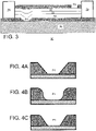
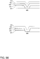
- FIG. 3 illustrates a portion of a solid-state electroactive device 30, in cross-section, having an improved film structure.
- the electroactive device 30 depicted in FIG. 3 is an electrochromic device similar to the device depicted in FIGS. 1 and 2 .
- teachings herein are similarly applicable to electrochromic devices with different stacks or film structures (e.g., additional layers).
- the electrochromic device 30 of FIG. 3 that device is similar to the device of FIGS. 1 and 2 only to the extent that each of the aforementioned layers, 11-15 are present in the device of FIG. 3 (as layers 31-35).
- the device of FIG. 3 differs from the device depicted in FIGS.
- the sidewall profile of the scribe at location P1 is shaped differently and has different properties or characteristics.
- the sidewall profile of the scribe in FIGS. 1 and 2 is substantially vertical or cliff-like
- the profile in FIG. 3 is tapered.
- the lower conductive layer of the device of FIGS. 1 and 2 is subject to delamination and melt spots along the scribe edges, whereas the improved device of FIG. 3 does not have delamination defects or melt spots.
- lower conductive layer 35 is formed on substrate 36 and includes a first portion coupled to a first busbar 38 and a second portion coupled to a second busbar 39.
- the first portion and second portion are physically separated from one another at location P1 by the scribe.
- the physical separation is covered and filled, either completely or partially, by the remaining layers of the electrochromic device, which include the electrode layer 34 formed directly thereon (which may be either the electrochromic electrode layer or the counter electrode layer), the ion conductor layer 33, the other electrode layer 32 (which may be the other of the electrochromic electrode layer and the counter electrode layer), and the upper conductive layer 31. Because of the tapered profile of the scribe sidewalls, which is relatively smooth compared to the scribe sidewalls of the device in FIGS.
- the electrode layer 34 provides improved step coverage along the scribe edge over the lower conductive layer.
- the ion conducting layer 13 shown in FIG. 2 reaches almost to the sidewall of the lower conductive layer 15, the electrode layer 34 in FIG. 3 maintains improved separation between the ion conducting layer 33 and the lower conductive layer 35.
- the electrode layers 32 and 34, and the ion conductor layer 33 sandwiched in between collectively provide improved step coverage along the scribe edge over the lower conductive layer 31 so that there are no current leaks or shorts between the respective conductive layers 31 and 35.
- each tapered sidewall may provide a smooth transition between the surface of the scribed layers and the surface of the substrate.
- each tapered sidewall may have a rounded upper edge.
- the overall slope of each tapered sidewall may be about 45 degrees with respect to the plane of the substrate.
- each tapered sidewall is formed such that no section of the sidewalls has a slope steeper than 45 degrees with respect to the plane of the substrate.
- FIGS. 4A-4C depict some possible sidewall profiles that may be achieved.
- FIG. 4A depicts a close-up of the linear profile of FIG. 3 .
- FIG. 4B depicts a substantially Gaussian (curved) profile with curved sidewall edges.
- FIG. 4C depicts a profile having both linear and curved properties.
- the energy profile of the beam may be smoothly varied.
- Fig. 3 highlights aspects of the invention, such as the tapered profile of the scribe sidewalls, and is useful for understanding the invention.
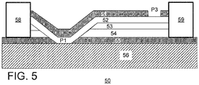
- FIG. 5 illustrates a portion of another solid-state electrochromic device 50, in cross-section, having another improved film structure.
- the device 50 of FIG. 5 is similar to the solid-state device depicted in FIG. 3 to the extent that each of the aforementioned layers, 31-35 is again present in the device of FIG. 5 (as layers 51-55).
- the device of FIG. 5 differs from the device depicted in FIG. 3 to the extent that the electrode layer directly adjacent to the lower conductive layer, and the ion conducting layer, have been scribed along with the lower conductive layer. Comparable to FIG. 3 , the sidewall profiles of the scribe at location PI is tapered. Also, like in FIG. 3 , each of the scribed layers of the device in FIG. 5 does not have delamination defects or melt spots.
- each of the lower conductive layer 55, first electrode layer 54, and ion conducting layer 53 is formed on substrate 56 and includes a first portion coupled to a first busbar 58 and a second portion coupled to a second busbar 59.
- the first portion and second portion of each layer are physically separated from one another at location PI by the scribe.
- the physical separation is covered and filled, either completely or partially, by the remaining layers, which include the electrode layer 52 (which may be either the electrochromic electrode layer or the counter electrode layer) and the upper conductive layer 51. Because of the tapered profile of the scribe sidewalls, which is relatively smooth compared to the scribe sidewalls of the device in FIGS. 1 and 2 , the electrode layer 52 provides improved step coverage along the scribe edge over the lower conductive layer 55 so that there are no current leaks or shorts between the respective conductive layers 51 and 55.
- the lower conductive layer, electrochromic electrode layer, and ion conductor layer are more than about twice as thick as the counterelectrode layer.
- the lower conductive layer, electrochromic electrode layer, and ion conductor layer may be more than about three times as thick as the counterelectrode layer.
- the lower conductive layer and one or more other scribed adjacent layers may be about twice as thick or more than the layers deposited over the scribed layers and underneath the upper conductive layer.
- the lower conductive layer and one or more other scribed adjacent layers may be about three times as thick or more than the layers deposited over the scribed layers and underneath the upper conductive layer.
- composition or type of layers which are deposited may be varied in order to achieve the desired results without departing from the teachings herein.
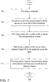
- FIG. 6 provides a flow diagram 600 that illustrates a process by which the device 30 may be formed.
- a substrate or workpiece on which the device will be formed or fabricated is provided.
- the substrate may be an ordinary piece of float glass, as is generally used in building windows, borosilicate glass, or other glass panes such as for automotive or aircraft applications.
- the substrate may be annealed, heat strengthened, thermally tempered, or chemically strengthened.
- the substrate may further include other materials suitable for the type of device being fabricated, including many transparent materials such as diamond, aluminum oxide or sapphire, and rigid or flexible polymers. Additionally, opaque materials with surfaces smooth enough to allow specular reflection may be used, when polished or coated to form a reflective background to the electroactive films, resulting in a reflective electroactive device. This could include metals with polished surfaces, and reflective metal or dielectric coatings on semiconductors or dielectrics, such as carbon, silicon, silicon carbide, gallium arsenide, or boron oxide.
- one or more adjacent layers of the electroactive device including a layer of conductive material, such as indium tin oxide, are formed on the surface of the substrate.
- the layers may be deposited such that each layer extends continuously from the first busbar to the second busbar of the device.
- the layers include the conductive layer.
- the layers further include an electrode layer which may be formed directly above and adjacent to the conductive layer.
- the materials comprising a conductive layer are deposited via sputtering onto a transparent substrate to form a transparent conductive layer.
- a scribing implement is positioned incident to the side of the substrate having the one or more adjacent layers formed thereon.
- the scribing implement may be capable of scribing the layers using one of several different methods, including laser scribing, mechanical abrading involving, for example, use of a diamond, ruby or stainless steel tip, electrical discharge machining, or chemical etching, or another suitable removing processes known in the art ("cutting").
- the scribing implement may be mounted in the deposition (e.g., coating) chamber. If the scribing implement is a laser, positioning of the laser may involve focusing a laser beam of the laser at location PI of the substrate.
- a portion of the one or more adjacent layers is removed using the scribing implement.
- the layers may scribed or cut at location PI.
- the scribe may extend the entire length of the substrate, i.e., from one end of the substrate to the opposite end, normal to the location P1 shown in the cross-section of FIG. 3 .
- the linewidth of the scribe may be about 25 microns or more.
- a scribe having a greater linewidth, or more than one scribe may be performed around location PI in accordance with the technology of copending U.S. Application Serial No. 13/950,791 .
- each scribe may be separated by unscribed material in the scribed layers.
- the multiples scribes could remove all of the material between each scribe, thereby resulting effectively in a single scribe having a relatively large linewidth compared to each individual scribe.
- the remaining layers may include the electrochromic electrode layer, the counter electrode layer, an ion conducting layer sandwiched between the two electrode layers, and an upper conducting layer formed above the other layers.
- Deposition of these layers may be performed by sputtering, chemical vapor deposition, or other thin film fabrication methods known in the art, such as those described in copending U.S. Application Serial No. 13/950,791 .
- additional layers may be formed in the layer structure, such as anti-reflective coating layers, optical tuning layers, such as those described in U.S. Patent No. 5,724,177 , ion transport layers, such as those described in U.S. Patent No. 8,004,744 .
- all of the adjacent scribed layers and at least one of the remaining layers are deposited via magnetron sputter deposition in the same vacuum processing chamber so as to increase device fabrication manufacturability, meaning that the substrate undergoes only one stage in coating the initial layers in the fabrication process of the device, that the yields are likely to be improved as a result of reduced handling, and further that the throughput is also likely to be increased as a result of fewer processing steps. Moreover, depositing all of the initial layers in the same chamber without removing the substrate results in a reduction in the number of shorts.
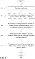
- FIG. 7 provides another flow diagram 700 that illustrates another process by which the device 30 may be formed.
- the steps described in blocks 702, 704, 708, and 710 are respectively comparable to steps 602, 604, 608, and 610 described in connection with flow diagram 600 and are therefore not repeated here.
- Flow diagram 700 includes an additional step, block 706, which may be performed in lieu or in addition to step 606 of flow diagram 600.
- a laser with a pulse width of about 100 picoseconds or shorter is provided.
- the laser may be positioned either incident or opposite the film side of the substrate. By positioning a laser having a pulse width of 100 picoseconds or shorter incident to the film side of the substrate, both flow diagrams 600 and 700 may be performed together.
- the pulse width of the laser may be selected to optimize dissipation of heat in the device during processing to prevent unwanted spreading of heat, which may cause delamination or melt spots in the lower conductive layer.
- a pulse width is generally about 100 picoseconds or shorter, but may vary depending on the materials being scribed. Generally, pulse widths lasting 1 nm or longer have been found to cause unwanted spreading of heat, but use of a laser having a shorter pulse width may be beneficial.
- the pulse width of the laser may be about 50 picoseconds or shorter. In further examples, the pulse width may be about 10 picoseconds or shorter. In yet further examples, the pulse width may be about 6 picoseconds.
- the wavelength of the laser may range from about 340 nm to about 1070 nm. More particularly, the wavelength of the laser may be selected to reduce absorption of the beam energy by the substrate, and more particularly to optimize the ratio of absorption between the lower conductive layer and the substrate. The optimal wavelength may vary depending on the substrate material and other layer materials. In some embodiments, the lower conductive layer should absorb a high percentage of the energy from the laser, and the substrate should absorb a low percentage of the energy. For example, in the electrochromic devices described in copending U.S. Application Serial No. 13/950,791 , it has been found that the glass substrates for electrochromic devices have a relatively low absorption of green light, and indium tin oxide on a glass substrate exhibits a higher ratio of absorption. Further, it has been found that light having a wavelength between about 515 nm and about 532 nm is preferred in such a device. In other devices using different materials, a laser emitting light having a different wavelength may be preferred.
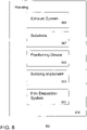
- FIG. 8 provides a simplified diagram of a system 800 for forming the electroactive device of the present disclosure.
- the system 800 includes a housing or chamber 810 for fabrication of the device.
- the chamber 810 may be any standard evaporation chamber or coater known in the art used for fabrication of electroactive devices.
- the chamber 810 may be a coater, such as for performing an initial stage of coating the conductive and/or electroactive layers on a substrate.
- the chamber 810 may be operated at either vacuum or under other pressure conditions (e.g., normal atmospheric pressure).
- Housed within the chamber 810 may be the film deposition system 801, the laser 803, a positioning device 805 for positioning or adjusting the position of beam of the laser relative to the substrate, the substrate 807, and a collection system 809.
- the film deposition system 801 may be a magnetron sputter, DC sputter, or RF sputter, or other means for depositing thin films of conductive and/or insulating materials on a substrate in vacuum conditions.
- the laser 803, as described above, may in some examples have a pulse width less than about 100 picoseconds.
- the positioning device 805 may hold the laser in place and/or mount the laser within the chamber, with the laser oriented such that it emits a laser beam at the surface of the substrate 807.
- the positioning device 805 may be configured such that the laser beam is incident to the film side of the substrate 807.
- the positioning device 805 may further be configured to displace or reorient the laser such that the focused beam may move along the scribe edge on the surface of the substrate 807.
- the collection system 809 may be a vent, electrostatic plate, chilled surface, pipe, or other structure for collecting particulate materials or vapors generated by focusing of the beam on the surface of the substrate.
- the collection system 809 may further be configured to filter those particulate materials or vapors, and/or carry them out of the housing 810. Collection and/or ejection of the particulate materials or vapors is beneficial for preventing materials from being 'blown' around during purging, venting, and/or pumpdown of the housing, which in turn could scratch or otherwise damage the substrate and/or film structure.
- the electroactive device may be formed without having to remove the substrate from the housing.
- the substrate may be placed in the housing, a layer of conductive material may be formed on the surface of the substrate, a portion of the layer of conductive material may be removed using the laser, and at least one of the electrochromic electrode layer and the counter electrode layer may be formed on the layer of conductive material, all without removing the substrate from the housing.
- these steps may be performed in a single continuous vacuum step.
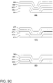
- the above described benefits may be realized in scribes through the conductive layer 911 only, such that the electrode layers and ion conductor layer 912-914 separate the upper and lower conductive layers, 915 and 911 respectively (910), or through the conductive layer 921 and one electrode layer 922, such that the emitting layer 923 and the other transport layer 924 separate the upper and lower conductive layers, 925 and 921 respectively (920), or even through the conductive layer 931, one electrode layer 932, and the ion conductor layer 933, such that only the other electrode layer 934 separates the upper and lower conductive layers, 935 and 931 respectively (930).
- the above described benefits may be realized in scribes through the conductive layer 941 only, such that the insulating layers and phosphor layer 942-944 separate the upper and lower conductive layers, 945 and 941 respectively (940), or through the conductive layer 951, one insulating layer 952, and the phosphor layer 953 (e.g., such that only the other insulating layer 954 separates the upper and lower conductive layers, 955 and 951 respectively) (950).
- the above described benefits may be realized in scribes through the conductive layer 961 only, such that the transporting layers and emitting layer 962-964 separate the upper and lower conductive layers, 965 and 961 respectively (960), or through the conductive layer and one transport layer, such that the emitting layer and the other transport layer separate the upper and lower conductive layers (not shown), or even through the conductive layer, one transport layer, and the emitting layer, such that only the other transport layer separates the upper and lower conductive layers (also not shown).
- the above described benefits may be realized in scribes through the conductive layer 971 only, such that the acceptor/donor layers and pn-junction layer 972-974 separate the upper and lower conductive layers, 975 and 971 respectively (970), or through the conductive layer 981, one of the acceptor/donor layers 982, and the p-n junction layer 983, such that only the other acceptor/donor layer 984 separates the upper and lower conductive layers, 985 and 981 respectively) (980).
- FIGS. 9A-C is depicted for illustrative clarity in the diagrams of FIGS. 9A-C .
- each of the above embodiments illustrates device structure between only two busbars, it will be understood that the above disclosure similarly applies to devices having more than two busbars as well.
- each of the busbars may be electrically separated from each other by forming the structures as described above. Forming of each of the structures may be performed simultaneously or sequentially, and the layers formed between each pair of busbars may be scribed in any of the manners described above.
- the embodiments described above are not limited to rectangular shaped devices. Rather, the descriptions and figures are meant only to depict cross-sectional views of a device and are not meant to limit the shape of such a device in any manner.
- the device may be formed in shapes other than rectangles (e.g., triangles, circles, arcuate structures, etc.).
- the device may be shaped three-dimensionally (e.g ., convex, concave, etc.).
Landscapes
- Physics & Mathematics (AREA)
- Optics & Photonics (AREA)
- Nonlinear Science (AREA)
- Engineering & Computer Science (AREA)
- Chemical & Material Sciences (AREA)
- General Physics & Mathematics (AREA)
- Mechanical Engineering (AREA)
- Materials Engineering (AREA)
- Chemical Kinetics & Catalysis (AREA)
- Metallurgy (AREA)
- Organic Chemistry (AREA)
- Plasma & Fusion (AREA)
- Electrochromic Elements, Electrophoresis, Or Variable Reflection Or Absorption Elements (AREA)
- Manufacturing & Machinery (AREA)
- Microelectronics & Electronic Packaging (AREA)
- Devices For Indicating Variable Information By Combining Individual Elements (AREA)
- Health & Medical Sciences (AREA)
- Toxicology (AREA)
- General Chemical & Material Sciences (AREA)
Applications Claiming Priority (2)
| Application Number | Priority Date | Filing Date | Title |
|---|---|---|---|
| US14/095,308 US20150153622A1 (en) | 2013-12-03 | 2013-12-03 | Methods for producing lower electrical isolation in electrochromic films |
| PCT/US2014/068357 WO2015084952A1 (en) | 2013-12-03 | 2014-12-03 | Electroactive device and a method of fabricating the same |
Publications (3)
| Publication Number | Publication Date |
|---|---|
| EP3078056A1 EP3078056A1 (en) | 2016-10-12 |
| EP3078056A4 EP3078056A4 (en) | 2017-07-19 |
| EP3078056B1 true EP3078056B1 (en) | 2022-09-14 |
Family
ID=53265206
Family Applications (1)
| Application Number | Title | Priority Date | Filing Date |
|---|---|---|---|
| EP14868114.1A Active EP3078056B1 (en) | 2013-12-03 | 2014-12-03 | Electroactive device and a method of fabricating the same |
Country Status (6)
Families Citing this family (15)
| Publication number | Priority date | Publication date | Assignee | Title |
|---|---|---|---|---|
| US9958750B2 (en) | 2010-11-08 | 2018-05-01 | View, Inc. | Electrochromic window fabrication methods |
| US10295880B2 (en) | 2011-12-12 | 2019-05-21 | View, Inc. | Narrow pre-deposition laser deletion |
| US12061402B2 (en) | 2011-12-12 | 2024-08-13 | View, Inc. | Narrow pre-deposition laser deletion |
| EP2791733B1 (en) | 2011-12-12 | 2017-10-25 | View, Inc. | Thin-film devices and fabrication |
| US12403676B2 (en) | 2011-12-12 | 2025-09-02 | View Operating Corporation | Thin-film devices and fabrication |
| US11865632B2 (en) | 2011-12-12 | 2024-01-09 | View, Inc. | Thin-film devices and fabrication |
| US10802371B2 (en) | 2011-12-12 | 2020-10-13 | View, Inc. | Thin-film devices and fabrication |
| US20150153622A1 (en) | 2013-12-03 | 2015-06-04 | Sage Electrochromics, Inc. | Methods for producing lower electrical isolation in electrochromic films |
| US12235560B2 (en) | 2014-11-25 | 2025-02-25 | View, Inc. | Faster switching electrochromic devices |
| CA2980477A1 (en) | 2015-03-20 | 2016-09-29 | View, Inc. | Faster switching low-defect electrochromic windows |
| WO2018157057A1 (en) | 2017-02-27 | 2018-08-30 | Sage Electrochromics, Inc. | Electrical device including a substrate and a transparent conductive layer and a process of forming the same |
| US20200096830A1 (en) * | 2018-09-26 | 2020-03-26 | Sage Electrochromics, Inc. | Electroactive device and methods |
| CN113574449A (zh) * | 2019-03-20 | 2021-10-29 | Sage电致变色显示有限公司 | 按库存生产的图案化透明导电层 |
| US20220198118A1 (en) * | 2020-12-21 | 2022-06-23 | Sage Electrochromics, Inc. | Apparatus and method for manufacturing a motherboard comprising one or more electrochromic devices |
| EP4609674A1 (en) * | 2022-11-10 | 2025-09-03 | Energy Materials Corporation | Photovoltaic modules and methods of making same |
Family Cites Families (42)
| Publication number | Priority date | Publication date | Assignee | Title |
|---|---|---|---|---|
| US5321544A (en) | 1991-09-04 | 1994-06-14 | Sun Active Glass Electrochromics, Inc. | Electrochromic structures and methods |
| US5724177A (en) | 1991-09-04 | 1998-03-03 | Sun Active Glass Electrochromics, Inc. | Electrochromic devices and methods |
| BR9306215A (pt) | 1992-04-10 | 1998-06-23 | Sun Active Glass Electrochrom | Dispositivo eletrocrómico e processo para a preparaçao do mesmo |
| US5370775A (en) | 1992-04-10 | 1994-12-06 | Sun Active Glass Electrochromics, Inc. | Formation of chemically reduced electrode layers |
| US5404244A (en) | 1992-04-10 | 1995-04-04 | Sun Active Glass Electrochromics, Inc. | Electrochromic structures and methods |
| US5724175A (en) * | 1997-01-02 | 1998-03-03 | Optical Coating Laboratory, Inc. | Electrochromic device manufacturing process |
| US6700692B2 (en) * | 1997-04-02 | 2004-03-02 | Gentex Corporation | Electrochromic rearview mirror assembly incorporating a display/signal light |
| US6515787B1 (en) * | 2000-03-07 | 2003-02-04 | Eclipse Energy Systems, Inc. | Electrochromic layer |
| JP4171166B2 (ja) * | 2000-08-31 | 2008-10-22 | 三洋電機株式会社 | 光起電力装置及びその製造方法 |
| US7255451B2 (en) * | 2002-09-20 | 2007-08-14 | Donnelly Corporation | Electro-optic mirror cell |
| FR2833107B1 (fr) | 2001-12-05 | 2004-02-20 | Saint Gobain | Electrode de dispositifs electrochimiques/electrocommandables |
| US6838157B2 (en) * | 2002-09-23 | 2005-01-04 | Siemens Westinghouse Power Corporation | Method and apparatus for instrumenting a gas turbine component having a barrier coating |
| JP2004198966A (ja) * | 2002-12-20 | 2004-07-15 | Tokai Rika Co Ltd | 反射鏡 |
| DE602004001508T2 (de) | 2003-01-31 | 2007-02-15 | Ntera Ltd. | Elektrochromische anzeigeeinrichtung |
| US6885033B2 (en) * | 2003-03-10 | 2005-04-26 | Cree, Inc. | Light emitting devices for light conversion and methods and semiconductor chips for fabricating the same |
| DE10333764B3 (de) | 2003-07-23 | 2004-12-30 | Outokumpu Oy | Verfahren zum Chargieren von feinkörnigen Metallen in einen Elektrolichtbogenofen |
| EP1557875A1 (en) * | 2003-12-29 | 2005-07-27 | STMicroelectronics S.r.l. | Process for forming tapered trenches in a dielectric material |
| US7372610B2 (en) | 2005-02-23 | 2008-05-13 | Sage Electrochromics, Inc. | Electrochromic devices and methods |
| US7593154B2 (en) | 2005-10-11 | 2009-09-22 | Sage Electrochromics, Inc. | Electrochromic devices having improved ion conducting layers |
| US7483454B2 (en) * | 2006-05-26 | 2009-01-27 | Hauck James P | Laser system architecture and method of using the same |
| US7749907B2 (en) | 2006-08-25 | 2010-07-06 | Semiconductor Energy Laboratory Co., Ltd. | Method for manufacturing semiconductor device |
| US8148259B2 (en) | 2006-08-30 | 2012-04-03 | Semiconductor Energy Laboratory Co., Ltd. | Method for manufacturing semiconductor device |
| JP5205042B2 (ja) | 2006-12-20 | 2013-06-05 | 株式会社半導体エネルギー研究所 | 半導体装置の作製方法 |
| US8168265B2 (en) * | 2008-06-06 | 2012-05-01 | Applied Materials, Inc. | Method for manufacturing electrochromic devices |
| JP5947546B2 (ja) * | 2009-02-05 | 2016-07-06 | コーニンクレッカ フィリップス エヌ ヴェKoninklijke Philips N.V. | エレクトロルミネッセント装置 |
| US8432603B2 (en) * | 2009-03-31 | 2013-04-30 | View, Inc. | Electrochromic devices |
| FR2944610B1 (fr) | 2009-04-16 | 2011-06-24 | Saint Gobain | Dispositif electrochrome a transparence controlee |
| JP5111450B2 (ja) * | 2009-06-23 | 2013-01-09 | 三菱電機株式会社 | 薄膜太陽電池およびその製造方法 |
| US20120318776A1 (en) * | 2009-09-24 | 2012-12-20 | Electro Scientific Industries, Inc. | Method and apparatus for machining a workpiece |
| US8493646B2 (en) * | 2010-04-22 | 2013-07-23 | Sage Electrochromics, Inc. | Series connected electrochromic devices |
| FR2962818B1 (fr) | 2010-07-13 | 2013-03-08 | Saint Gobain | Dispositif electrochimique a proprietes de transmission optique et/ou energetique electrocommandables. |
| KR101172178B1 (ko) * | 2010-09-01 | 2012-08-07 | 엘지이노텍 주식회사 | 태양광 발전장치 및 이의 제조방법 |
| US8134067B1 (en) * | 2011-01-21 | 2012-03-13 | Chin-Yao Tsai | Thin film photovoltaic device |
| US10429712B2 (en) * | 2012-04-20 | 2019-10-01 | View, Inc. | Angled bus bar |
| JP2012243864A (ja) * | 2011-05-17 | 2012-12-10 | Mitsubishi Electric Corp | 集積型薄膜太陽電池とその製造方法及びそのレーザ加工方法 |
| WO2012174393A1 (en) * | 2011-06-17 | 2012-12-20 | Sion Power Corporation | Plating technique for electrode |
| EP2791733B1 (en) * | 2011-12-12 | 2017-10-25 | View, Inc. | Thin-film devices and fabrication |
| US8652940B2 (en) * | 2012-04-10 | 2014-02-18 | Applied Materials, Inc. | Wafer dicing used hybrid multi-step laser scribing process with plasma etch |
| EP2841987B1 (en) * | 2012-04-25 | 2020-01-22 | View, Inc. | Electrochromic window fabrication method and electrochromic window |
| US9013778B2 (en) * | 2013-03-06 | 2015-04-21 | Sage Electrochromics, Inc. | Laser cuts to reduce electrical leakage |
| US9152001B2 (en) | 2013-07-25 | 2015-10-06 | Sage Electrochromics, Inc. | Electrochromic devices having improved structure for reducing current leakage across lower transparent conductor layers |
| US20150153622A1 (en) | 2013-12-03 | 2015-06-04 | Sage Electrochromics, Inc. | Methods for producing lower electrical isolation in electrochromic films |
-
2013
- 2013-12-03 US US14/095,308 patent/US20150153622A1/en not_active Abandoned
-
2014
- 2014-12-03 CN CN201480066044.2A patent/CN105793965A/zh active Pending
- 2014-12-03 DK DK14868114.1T patent/DK3078056T3/da active
- 2014-12-03 CN CN202110412133.XA patent/CN113093445A/zh active Pending
- 2014-12-03 WO PCT/US2014/068357 patent/WO2015084952A1/en active Application Filing
- 2014-12-03 JP JP2016534714A patent/JP6340079B2/ja not_active Expired - Fee Related
- 2014-12-03 EP EP14868114.1A patent/EP3078056B1/en active Active
-
2017
- 2017-02-22 US US15/439,612 patent/US11194211B2/en active Active
-
2021
- 2021-11-08 US US17/453,971 patent/US12360426B2/en active Active
Also Published As
| Publication number | Publication date |
|---|---|
| US20150153622A1 (en) | 2015-06-04 |
| US20220057686A1 (en) | 2022-02-24 |
| DK3078056T3 (da) | 2022-11-21 |
| US20170160619A1 (en) | 2017-06-08 |
| US12360426B2 (en) | 2025-07-15 |
| CN105793965A (zh) | 2016-07-20 |
| CN113093445A (zh) | 2021-07-09 |
| EP3078056A1 (en) | 2016-10-12 |
| US11194211B2 (en) | 2021-12-07 |
| JP6340079B2 (ja) | 2018-06-06 |
| JP2016540248A (ja) | 2016-12-22 |
| EP3078056A4 (en) | 2017-07-19 |
| WO2015084952A1 (en) | 2015-06-11 |
Similar Documents
| Publication | Publication Date | Title |
|---|---|---|
| US12360426B2 (en) | Methods for producing lower electrical isolation in electrochromic films | |
| TWI628499B (zh) | 電致變色裝置及製造彼之方法及裝置 | |
| US8693078B2 (en) | Electrochromic devices | |
| US9252320B2 (en) | Thin film structures and devices with integrated light and heat blocking layers for laser patterning | |
| US20220308416A1 (en) | Electrochromic cathode materials | |
| JP2020536290A (ja) | 非発光式の可変透過デバイス及びそれを形成する方法 | |
| US8692153B2 (en) | Method for manufacturing photoelectric-conversion-device, device for photoelectric-conversion-device manufacturing device, and photoelectric conversion device | |
| TWI433340B (zh) | 半導體元件以及增加半導體元件有效運作面積的方法 | |
| JP6392346B2 (ja) | 下部透明導体層の部分を通る電流漏れを低減するように改良された構造を有するエレクトロクロミックデバイス | |
| KR20170086631A (ko) | 전기변색 디바이스들을 위한 상대 전극 | |
| KR20220120709A (ko) | 박막 디바이스 및 제조 | |
| US8779282B2 (en) | Solar cell apparatus and method for manufacturing the same | |
| US8835253B2 (en) | Photoelectric conversion device fabrication method and photoelectric conversion device | |
| CN103094408B (zh) | 太阳能电池及其制造方法以及太阳能电池图案 | |
| CN111886698A (zh) | 产生薄膜太阳能模块的方法 | |
| KR101938727B1 (ko) | 기판 구조체 및 이를 이용한 박막 태양전지 |
Legal Events
| Date | Code | Title | Description |
|---|---|---|---|
| PUAI | Public reference made under article 153(3) epc to a published international application that has entered the european phase |
Free format text: ORIGINAL CODE: 0009012 |
|
| 17P | Request for examination filed |
Effective date: 20160622 |
|
| AK | Designated contracting states |
Kind code of ref document: A1 Designated state(s): AL AT BE BG CH CY CZ DE DK EE ES FI FR GB GR HR HU IE IS IT LI LT LU LV MC MK MT NL NO PL PT RO RS SE SI SK SM TR |
|
| AX | Request for extension of the european patent |
Extension state: BA ME |
|
| DAX | Request for extension of the european patent (deleted) | ||
| RIC1 | Information provided on ipc code assigned before grant |
Ipc: G02F 1/153 20060101ALI20170608BHEP Ipc: H01L 21/28 20060101ALI20170608BHEP Ipc: H01L 21/3205 20060101AFI20170608BHEP |
|
| A4 | Supplementary search report drawn up and despatched |
Effective date: 20170619 |
|
| STAA | Information on the status of an ep patent application or granted ep patent |
Free format text: STATUS: EXAMINATION IS IN PROGRESS |
|
| 17Q | First examination report despatched |
Effective date: 20190402 |
|
| GRAP | Despatch of communication of intention to grant a patent |
Free format text: ORIGINAL CODE: EPIDOSNIGR1 |
|
| STAA | Information on the status of an ep patent application or granted ep patent |
Free format text: STATUS: GRANT OF PATENT IS INTENDED |
|
| INTG | Intention to grant announced |
Effective date: 20210507 |
|
| GRAJ | Information related to disapproval of communication of intention to grant by the applicant or resumption of examination proceedings by the epo deleted |
Free format text: ORIGINAL CODE: EPIDOSDIGR1 |
|
| STAA | Information on the status of an ep patent application or granted ep patent |
Free format text: STATUS: EXAMINATION IS IN PROGRESS |
|
| INTC | Intention to grant announced (deleted) | ||
| GRAP | Despatch of communication of intention to grant a patent |
Free format text: ORIGINAL CODE: EPIDOSNIGR1 |
|
| STAA | Information on the status of an ep patent application or granted ep patent |
Free format text: STATUS: GRANT OF PATENT IS INTENDED |
|
| INTG | Intention to grant announced |
Effective date: 20210927 |
|
| GRAJ | Information related to disapproval of communication of intention to grant by the applicant or resumption of examination proceedings by the epo deleted |
Free format text: ORIGINAL CODE: EPIDOSDIGR1 |
|
| STAA | Information on the status of an ep patent application or granted ep patent |
Free format text: STATUS: EXAMINATION IS IN PROGRESS |
|
| INTC | Intention to grant announced (deleted) | ||
| GRAP | Despatch of communication of intention to grant a patent |
Free format text: ORIGINAL CODE: EPIDOSNIGR1 |
|
| STAA | Information on the status of an ep patent application or granted ep patent |
Free format text: STATUS: GRANT OF PATENT IS INTENDED |
|
| INTG | Intention to grant announced |
Effective date: 20220309 |
|
| GRAJ | Information related to disapproval of communication of intention to grant by the applicant or resumption of examination proceedings by the epo deleted |
Free format text: ORIGINAL CODE: EPIDOSDIGR1 |
|
| STAA | Information on the status of an ep patent application or granted ep patent |
Free format text: STATUS: EXAMINATION IS IN PROGRESS |
|
| INTC | Intention to grant announced (deleted) | ||
| INTG | Intention to grant announced |
Effective date: 20220510 |
|
| GRAS | Grant fee paid |
Free format text: ORIGINAL CODE: EPIDOSNIGR3 |
|
| STAA | Information on the status of an ep patent application or granted ep patent |
Free format text: STATUS: GRANT OF PATENT IS INTENDED |
|
| GRAA | (expected) grant |
Free format text: ORIGINAL CODE: 0009210 |
|
| STAA | Information on the status of an ep patent application or granted ep patent |
Free format text: STATUS: THE PATENT HAS BEEN GRANTED |
|
| AK | Designated contracting states |
Kind code of ref document: B1 Designated state(s): AL AT BE BG CH CY CZ DE DK EE ES FI FR GB GR HR HU IE IS IT LI LT LU LV MC MK MT NL NO PL PT RO RS SE SI SK SM TR |
|
| REG | Reference to a national code |
Ref country code: GB Ref legal event code: FG4D |
|
| REG | Reference to a national code |
Ref country code: CH Ref legal event code: EP |
|
| REG | Reference to a national code |
Ref country code: DE Ref legal event code: R096 Ref document number: 602014084974 Country of ref document: DE |
|
| REG | Reference to a national code |
Ref country code: IE Ref legal event code: FG4D |
|
| REG | Reference to a national code |
Ref country code: AT Ref legal event code: REF Ref document number: 1519230 Country of ref document: AT Kind code of ref document: T Effective date: 20221015 |
|
| REG | Reference to a national code |
Ref country code: DK Ref legal event code: T3 Effective date: 20221116 |
|
| REG | Reference to a national code |
Ref country code: NL Ref legal event code: FP |
|
| REG | Reference to a national code |
Ref country code: SE Ref legal event code: TRGR |
|
| REG | Reference to a national code |
Ref country code: LT Ref legal event code: MG9D |
|
| PG25 | Lapsed in a contracting state [announced via postgrant information from national office to epo] |
Ref country code: RS Free format text: LAPSE BECAUSE OF FAILURE TO SUBMIT A TRANSLATION OF THE DESCRIPTION OR TO PAY THE FEE WITHIN THE PRESCRIBED TIME-LIMIT Effective date: 20220914 Ref country code: NO Free format text: LAPSE BECAUSE OF FAILURE TO SUBMIT A TRANSLATION OF THE DESCRIPTION OR TO PAY THE FEE WITHIN THE PRESCRIBED TIME-LIMIT Effective date: 20221214 Ref country code: LV Free format text: LAPSE BECAUSE OF FAILURE TO SUBMIT A TRANSLATION OF THE DESCRIPTION OR TO PAY THE FEE WITHIN THE PRESCRIBED TIME-LIMIT Effective date: 20220914 Ref country code: LT Free format text: LAPSE BECAUSE OF FAILURE TO SUBMIT A TRANSLATION OF THE DESCRIPTION OR TO PAY THE FEE WITHIN THE PRESCRIBED TIME-LIMIT Effective date: 20220914 Ref country code: FI Free format text: LAPSE BECAUSE OF FAILURE TO SUBMIT A TRANSLATION OF THE DESCRIPTION OR TO PAY THE FEE WITHIN THE PRESCRIBED TIME-LIMIT Effective date: 20220914 |
|
| PGFP | Annual fee paid to national office [announced via postgrant information from national office to epo] |
Ref country code: SE Payment date: 20221124 Year of fee payment: 9 Ref country code: DK Payment date: 20221123 Year of fee payment: 9 |
|
| REG | Reference to a national code |
Ref country code: AT Ref legal event code: MK05 Ref document number: 1519230 Country of ref document: AT Kind code of ref document: T Effective date: 20220914 |
|
| PG25 | Lapsed in a contracting state [announced via postgrant information from national office to epo] |
Ref country code: HR Free format text: LAPSE BECAUSE OF FAILURE TO SUBMIT A TRANSLATION OF THE DESCRIPTION OR TO PAY THE FEE WITHIN THE PRESCRIBED TIME-LIMIT Effective date: 20220914 Ref country code: GR Free format text: LAPSE BECAUSE OF FAILURE TO SUBMIT A TRANSLATION OF THE DESCRIPTION OR TO PAY THE FEE WITHIN THE PRESCRIBED TIME-LIMIT Effective date: 20221215 |
|
| PG25 | Lapsed in a contracting state [announced via postgrant information from national office to epo] |
Ref country code: SM Free format text: LAPSE BECAUSE OF FAILURE TO SUBMIT A TRANSLATION OF THE DESCRIPTION OR TO PAY THE FEE WITHIN THE PRESCRIBED TIME-LIMIT Effective date: 20220914 Ref country code: RO Free format text: LAPSE BECAUSE OF FAILURE TO SUBMIT A TRANSLATION OF THE DESCRIPTION OR TO PAY THE FEE WITHIN THE PRESCRIBED TIME-LIMIT Effective date: 20220914 Ref country code: PT Free format text: LAPSE BECAUSE OF FAILURE TO SUBMIT A TRANSLATION OF THE DESCRIPTION OR TO PAY THE FEE WITHIN THE PRESCRIBED TIME-LIMIT Effective date: 20230116 Ref country code: ES Free format text: LAPSE BECAUSE OF FAILURE TO SUBMIT A TRANSLATION OF THE DESCRIPTION OR TO PAY THE FEE WITHIN THE PRESCRIBED TIME-LIMIT Effective date: 20220914 Ref country code: CZ Free format text: LAPSE BECAUSE OF FAILURE TO SUBMIT A TRANSLATION OF THE DESCRIPTION OR TO PAY THE FEE WITHIN THE PRESCRIBED TIME-LIMIT Effective date: 20220914 Ref country code: AT Free format text: LAPSE BECAUSE OF FAILURE TO SUBMIT A TRANSLATION OF THE DESCRIPTION OR TO PAY THE FEE WITHIN THE PRESCRIBED TIME-LIMIT Effective date: 20220914 |
|
| PG25 | Lapsed in a contracting state [announced via postgrant information from national office to epo] |
Ref country code: SK Free format text: LAPSE BECAUSE OF FAILURE TO SUBMIT A TRANSLATION OF THE DESCRIPTION OR TO PAY THE FEE WITHIN THE PRESCRIBED TIME-LIMIT Effective date: 20220914 Ref country code: PL Free format text: LAPSE BECAUSE OF FAILURE TO SUBMIT A TRANSLATION OF THE DESCRIPTION OR TO PAY THE FEE WITHIN THE PRESCRIBED TIME-LIMIT Effective date: 20220914 Ref country code: IS Free format text: LAPSE BECAUSE OF FAILURE TO SUBMIT A TRANSLATION OF THE DESCRIPTION OR TO PAY THE FEE WITHIN THE PRESCRIBED TIME-LIMIT Effective date: 20230114 Ref country code: EE Free format text: LAPSE BECAUSE OF FAILURE TO SUBMIT A TRANSLATION OF THE DESCRIPTION OR TO PAY THE FEE WITHIN THE PRESCRIBED TIME-LIMIT Effective date: 20220914 |
|
| REG | Reference to a national code |
Ref country code: DE Ref legal event code: R097 Ref document number: 602014084974 Country of ref document: DE |
|
| PG25 | Lapsed in a contracting state [announced via postgrant information from national office to epo] |
Ref country code: AL Free format text: LAPSE BECAUSE OF FAILURE TO SUBMIT A TRANSLATION OF THE DESCRIPTION OR TO PAY THE FEE WITHIN THE PRESCRIBED TIME-LIMIT Effective date: 20220914 |
|
| P01 | Opt-out of the competence of the unified patent court (upc) registered |
Effective date: 20230530 |
|
| PLBE | No opposition filed within time limit |
Free format text: ORIGINAL CODE: 0009261 |
|
| STAA | Information on the status of an ep patent application or granted ep patent |
Free format text: STATUS: NO OPPOSITION FILED WITHIN TIME LIMIT |
|
| 26N | No opposition filed |
Effective date: 20230615 |
|
| PG25 | Lapsed in a contracting state [announced via postgrant information from national office to epo] |
Ref country code: SI Free format text: LAPSE BECAUSE OF FAILURE TO SUBMIT A TRANSLATION OF THE DESCRIPTION OR TO PAY THE FEE WITHIN THE PRESCRIBED TIME-LIMIT Effective date: 20220914 Ref country code: LU Free format text: LAPSE BECAUSE OF NON-PAYMENT OF DUE FEES Effective date: 20221203 |
|
| PG25 | Lapsed in a contracting state [announced via postgrant information from national office to epo] |
Ref country code: IE Free format text: LAPSE BECAUSE OF NON-PAYMENT OF DUE FEES Effective date: 20221203 |
|
| PGFP | Annual fee paid to national office [announced via postgrant information from national office to epo] |
Ref country code: NL Payment date: 20231121 Year of fee payment: 10 |
|
| PGFP | Annual fee paid to national office [announced via postgrant information from national office to epo] |
Ref country code: GB Payment date: 20231121 Year of fee payment: 10 |
|
| PGFP | Annual fee paid to national office [announced via postgrant information from national office to epo] |
Ref country code: BE Payment date: 20231121 Year of fee payment: 10 |
|
| PG25 | Lapsed in a contracting state [announced via postgrant information from national office to epo] |
Ref country code: HU Free format text: LAPSE BECAUSE OF FAILURE TO SUBMIT A TRANSLATION OF THE DESCRIPTION OR TO PAY THE FEE WITHIN THE PRESCRIBED TIME-LIMIT; INVALID AB INITIO Effective date: 20141203 |
|
| PG25 | Lapsed in a contracting state [announced via postgrant information from national office to epo] |
Ref country code: CY Free format text: LAPSE BECAUSE OF FAILURE TO SUBMIT A TRANSLATION OF THE DESCRIPTION OR TO PAY THE FEE WITHIN THE PRESCRIBED TIME-LIMIT Effective date: 20220914 |
|
| PG25 | Lapsed in a contracting state [announced via postgrant information from national office to epo] |
Ref country code: MK Free format text: LAPSE BECAUSE OF FAILURE TO SUBMIT A TRANSLATION OF THE DESCRIPTION OR TO PAY THE FEE WITHIN THE PRESCRIBED TIME-LIMIT Effective date: 20220914 Ref country code: IT Free format text: LAPSE BECAUSE OF FAILURE TO SUBMIT A TRANSLATION OF THE DESCRIPTION OR TO PAY THE FEE WITHIN THE PRESCRIBED TIME-LIMIT Effective date: 20220914 |
|
| PG25 | Lapsed in a contracting state [announced via postgrant information from national office to epo] |
Ref country code: MC Free format text: LAPSE BECAUSE OF FAILURE TO SUBMIT A TRANSLATION OF THE DESCRIPTION OR TO PAY THE FEE WITHIN THE PRESCRIBED TIME-LIMIT Effective date: 20220914 |
|
| PG25 | Lapsed in a contracting state [announced via postgrant information from national office to epo] |
Ref country code: MC Free format text: LAPSE BECAUSE OF FAILURE TO SUBMIT A TRANSLATION OF THE DESCRIPTION OR TO PAY THE FEE WITHIN THE PRESCRIBED TIME-LIMIT Effective date: 20220914 |
|
| REG | Reference to a national code |
Ref country code: DK Ref legal event code: EBP Effective date: 20231231 |
|
| REG | Reference to a national code |
Ref country code: SE Ref legal event code: EUG |
|
| PG25 | Lapsed in a contracting state [announced via postgrant information from national office to epo] |
Ref country code: BG Free format text: LAPSE BECAUSE OF FAILURE TO SUBMIT A TRANSLATION OF THE DESCRIPTION OR TO PAY THE FEE WITHIN THE PRESCRIBED TIME-LIMIT Effective date: 20220914 |
|
| PG25 | Lapsed in a contracting state [announced via postgrant information from national office to epo] |
Ref country code: MT Free format text: LAPSE BECAUSE OF FAILURE TO SUBMIT A TRANSLATION OF THE DESCRIPTION OR TO PAY THE FEE WITHIN THE PRESCRIBED TIME-LIMIT Effective date: 20220914 |
|
| PGFP | Annual fee paid to national office [announced via postgrant information from national office to epo] |
Ref country code: DE Payment date: 20241121 Year of fee payment: 11 |
|
| PG25 | Lapsed in a contracting state [announced via postgrant information from national office to epo] |
Ref country code: DK Free format text: LAPSE BECAUSE OF NON-PAYMENT OF DUE FEES Effective date: 20231231 |
|
| PGFP | Annual fee paid to national office [announced via postgrant information from national office to epo] |
Ref country code: FR Payment date: 20241121 Year of fee payment: 11 |
|
| PG25 | Lapsed in a contracting state [announced via postgrant information from national office to epo] |
Ref country code: DK Free format text: LAPSE BECAUSE OF NON-PAYMENT OF DUE FEES Effective date: 20231231 |
|
| PGFP | Annual fee paid to national office [announced via postgrant information from national office to epo] |
Ref country code: CH Payment date: 20250101 Year of fee payment: 11 |
|
| REG | Reference to a national code |
Ref country code: NL Ref legal event code: MM Effective date: 20250101 |
|
| GBPC | Gb: european patent ceased through non-payment of renewal fee |
Effective date: 20241203 |