EP3076445A2 - Thermoelectric converter and dehumidifier using the same - Google Patents
Thermoelectric converter and dehumidifier using the same Download PDFInfo
- Publication number
- EP3076445A2 EP3076445A2 EP16163230.2A EP16163230A EP3076445A2 EP 3076445 A2 EP3076445 A2 EP 3076445A2 EP 16163230 A EP16163230 A EP 16163230A EP 3076445 A2 EP3076445 A2 EP 3076445A2
- Authority
- EP
- European Patent Office
- Prior art keywords
- thermoelectric
- substrate
- thermoelectric conversion
- conversion member
- disposed
- Prior art date
- Legal status (The legal status is an assumption and is not a legal conclusion. Google has not performed a legal analysis and makes no representation as to the accuracy of the status listed.)
- Granted
Links
Images


Classifications
-
- H—ELECTRICITY
- H10—SEMICONDUCTOR DEVICES; ELECTRIC SOLID-STATE DEVICES NOT OTHERWISE PROVIDED FOR
- H10N—ELECTRIC SOLID-STATE DEVICES NOT OTHERWISE PROVIDED FOR
- H10N10/00—Thermoelectric devices comprising a junction of dissimilar materials, i.e. devices exhibiting Seebeck or Peltier effects
- H10N10/80—Constructional details
-
- F—MECHANICAL ENGINEERING; LIGHTING; HEATING; WEAPONS; BLASTING
- F24—HEATING; RANGES; VENTILATING
- F24F—AIR-CONDITIONING; AIR-HUMIDIFICATION; VENTILATION; USE OF AIR CURRENTS FOR SCREENING
- F24F5/00—Air-conditioning systems or apparatus not covered by F24F1/00 or F24F3/00, e.g. using solar heat or combined with household units such as an oven or water heater
- F24F5/0042—Air-conditioning systems or apparatus not covered by F24F1/00 or F24F3/00, e.g. using solar heat or combined with household units such as an oven or water heater characterised by the application of thermo-electric units or the Peltier effect
-
- F—MECHANICAL ENGINEERING; LIGHTING; HEATING; WEAPONS; BLASTING
- F25—REFRIGERATION OR COOLING; COMBINED HEATING AND REFRIGERATION SYSTEMS; HEAT PUMP SYSTEMS; MANUFACTURE OR STORAGE OF ICE; LIQUEFACTION SOLIDIFICATION OF GASES
- F25B—REFRIGERATION MACHINES, PLANTS OR SYSTEMS; COMBINED HEATING AND REFRIGERATION SYSTEMS; HEAT PUMP SYSTEMS
- F25B21/00—Machines, plants or systems, using electric or magnetic effects
- F25B21/02—Machines, plants or systems, using electric or magnetic effects using Peltier effect; using Nernst-Ettinghausen effect
- F25B21/04—Machines, plants or systems, using electric or magnetic effects using Peltier effect; using Nernst-Ettinghausen effect reversible
-
- F—MECHANICAL ENGINEERING; LIGHTING; HEATING; WEAPONS; BLASTING
- F24—HEATING; RANGES; VENTILATING
- F24F—AIR-CONDITIONING; AIR-HUMIDIFICATION; VENTILATION; USE OF AIR CURRENTS FOR SCREENING
- F24F3/00—Air-conditioning systems in which conditioned primary air is supplied from one or more central stations to distributing units in the rooms or spaces where it may receive secondary treatment; Apparatus specially designed for such systems
- F24F3/12—Air-conditioning systems in which conditioned primary air is supplied from one or more central stations to distributing units in the rooms or spaces where it may receive secondary treatment; Apparatus specially designed for such systems characterised by the treatment of the air otherwise than by heating and cooling
- F24F3/14—Air-conditioning systems in which conditioned primary air is supplied from one or more central stations to distributing units in the rooms or spaces where it may receive secondary treatment; Apparatus specially designed for such systems characterised by the treatment of the air otherwise than by heating and cooling by humidification; by dehumidification
-
- H—ELECTRICITY
- H10—SEMICONDUCTOR DEVICES; ELECTRIC SOLID-STATE DEVICES NOT OTHERWISE PROVIDED FOR
- H10N—ELECTRIC SOLID-STATE DEVICES NOT OTHERWISE PROVIDED FOR
- H10N10/00—Thermoelectric devices comprising a junction of dissimilar materials, i.e. devices exhibiting Seebeck or Peltier effects
- H10N10/10—Thermoelectric devices comprising a junction of dissimilar materials, i.e. devices exhibiting Seebeck or Peltier effects operating with only the Peltier or Seebeck effects
- H10N10/13—Thermoelectric devices comprising a junction of dissimilar materials, i.e. devices exhibiting Seebeck or Peltier effects operating with only the Peltier or Seebeck effects characterised by the heat-exchanging means at the junction
-
- H—ELECTRICITY
- H10—SEMICONDUCTOR DEVICES; ELECTRIC SOLID-STATE DEVICES NOT OTHERWISE PROVIDED FOR
- H10N—ELECTRIC SOLID-STATE DEVICES NOT OTHERWISE PROVIDED FOR
- H10N10/00—Thermoelectric devices comprising a junction of dissimilar materials, i.e. devices exhibiting Seebeck or Peltier effects
- H10N10/10—Thermoelectric devices comprising a junction of dissimilar materials, i.e. devices exhibiting Seebeck or Peltier effects operating with only the Peltier or Seebeck effects
- H10N10/17—Thermoelectric devices comprising a junction of dissimilar materials, i.e. devices exhibiting Seebeck or Peltier effects operating with only the Peltier or Seebeck effects characterised by the structure or configuration of the cell or thermocouple forming the device
-
- H—ELECTRICITY
- H10—SEMICONDUCTOR DEVICES; ELECTRIC SOLID-STATE DEVICES NOT OTHERWISE PROVIDED FOR
- H10N—ELECTRIC SOLID-STATE DEVICES NOT OTHERWISE PROVIDED FOR
- H10N10/00—Thermoelectric devices comprising a junction of dissimilar materials, i.e. devices exhibiting Seebeck or Peltier effects
- H10N10/80—Constructional details
- H10N10/85—Thermoelectric active materials
- H10N10/851—Thermoelectric active materials comprising inorganic compositions
- H10N10/852—Thermoelectric active materials comprising inorganic compositions comprising tellurium, selenium or sulfur
-
- H—ELECTRICITY
- H10—SEMICONDUCTOR DEVICES; ELECTRIC SOLID-STATE DEVICES NOT OTHERWISE PROVIDED FOR
- H10N—ELECTRIC SOLID-STATE DEVICES NOT OTHERWISE PROVIDED FOR
- H10N10/00—Thermoelectric devices comprising a junction of dissimilar materials, i.e. devices exhibiting Seebeck or Peltier effects
- H10N10/80—Constructional details
- H10N10/85—Thermoelectric active materials
- H10N10/851—Thermoelectric active materials comprising inorganic compositions
- H10N10/853—Thermoelectric active materials comprising inorganic compositions comprising arsenic, antimony or bismuth
Abstract
Description
- This application claims priority to and the benefit of Korean Patent Application No.
2015-0045533, filed on March 31, 2015 - Embodiments of the present invention relate to a device structure capable of improving cooling efficiency.
- Dehumidification is a principle of removing moisture in the air using a condensation phenomenon in which moisture in the air is condensed to water using a temperature difference, and a device using this principle is a dehumidifier. Nowadays, in indoor spaces such as households or offices, in addition to demands on a humidifier that maintains humidity of a dry indoor space, demands on the dehumidifier that removes humidity of a damp indoor space to keep the indoor space pleasant is increasing.
- So far, a cooling dehumidification method also referred to as a compressor method that dehumidifies by taking heat away and a heating dehumidification method also referred to as a desiccant method that dehumidifies using heat have been mainly used as methods of dehumidification.
- Particularly, in case of the method using a compressor, since moisture in humid air is first condensed and discharged using a refrigerant and the air is dried again, a dehumidification effect depends on the capacity of the compressor, thus imposing a limitation in the dehumidification effect, and there is a major problem of an increase in noise due to excessive operation of the compressor for dehumidification up to capacity limit.
- Embodiments of the present invention are devised for resolving the problems mentioned above, and particularly, the present invention is directed to providing a thermoelectric converter implementing a structure in which two or more thermoelectric modules are stacked and cooling areas of the stacked thermoelectric modules are arranged in a compact structure to maximize cooling efficiency.
- Particularly, a thermoelectric converter with enhanced cooling efficiency is applied to a dehumidifier to remove a compressor of a conventional compressor structure and to implement a dehumidifier only with a thermoelectric module having a structure that does not use chemical refrigerant at all.
- A thermoelectric converter according to an embodiment of the present invention includes a first thermoelectric module including a first substrate, a second substrate disposed to face the first substrate, and a first thermoelectric element disposed between the first substrate and the second substrate; a first thermoelectric conversion member disposed on the first substrate; a second thermoelectric conversion member disposed on the second substrate; a second thermoelectric module including a third substrate, a fourth substrate disposed to face the third substrate, and a second thermoelectric element disposed between the third substrate and the fourth substrate; a third thermoelectric conversion member disposed on the third substrate; and a fourth thermoelectric conversion member disposed on the fourth substrate, wherein the first substrate and the third substrate may be heat generation substrates, the second substrate and the fourth substrate may be heat absorption substrates, and the first thermoelectric module and the second thermoelectric module may be arranged in a structure in which the second substrate and the fourth substrate face each other.
- The above and other objects, features and advantages of the present invention will become more apparent to those of ordinary skill in the art by describing in detail exemplary embodiments thereof with reference to the accompanying drawings, in which:
-
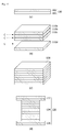
FIG. 1 is a cross-sectional view of a thermoelectric converter according to an embodiment of the present invention; -
FIG. 2 is an exploded perspective view of the thermoelectric converter illustrated inFIG. 1 ; -
FIG. 3 illustrates an arrangement of thermoelectric conversion members sandwiching a first thermoelectric module at one portion of the structure of the thermoelectric converter illustrated inFIG. 1 ; -
FIG. 4 is an enlarged perspective view exploded from a main portion ofFIG. 3 ; -
FIGS. 5 and6 illustrate an embodiment of a structure of a thermoelectric conversion member according toFIGS. 3 and4 ; -
FIG. 7 illustrates an example of implementing a thermoelectric conversion module in a structure according to an embodiment different from the structure of the thermoelectric conversion member mentioned inFIG. 6 ; -
FIGS. 8 and9 are conceptual views illustrating a structure of a thermoelectric module applied to the thermoelectric converter according to the embodiment of the present invention; -
FIG. 10 illustrates a modified embodiment in which a shape of the thermoelectric element mentioned inFIG. 9 is changed; and -
FIGS. 11 to 13 are conceptual views illustrating another embodiment of a thermoelectric element applied to the thermoelectric converter according to the embodiment of the present invention. - Hereinafter, configurations and actions according to the present invention will be described in detail with reference to the accompanying drawings. In describing the present invention with reference to the accompanying drawings, like reference numerals will be given to like elements throughout the drawings and overlapping descriptions thereof will be omitted. Terms such as "first" and "second" may be used in describing various elements, but the elements should not be limited by the terms. The terms are used only for differentiating one element from another element.
-
FIG. 1 is a cross-sectional view of athermoelectric converter 10 according to an embodiment of the present invention.FIG. 2 is an exploded perspective view of thethermoelectric converter 10 illustrated inFIG. 1 .FIG. 3 illustrates an arrangement ofthermoelectric conversion members thermoelectric module 100 at one portion of the structure of thethermoelectric converter 10 illustrated inFIG. 1 .FIG. 4 is an enlarged perspective view exploded from a main portion ofFIG. 3 . - Referring to
FIGS. 1 and2 , thethermoelectric converter 10 according to the embodiment of the present invention includes the firstthermoelectric module 100, a secondthermoelectric module 400, a firstthermoelectric conversion member 220, a secondthermoelectric conversion member 320, a thirdthermoelectric conversion member 620, and a fourththermoelectric conversion member 520. - The first
thermoelectric module 100 may include afirst substrate 140, asecond substrate 150 disposed to face thefirst substrate 140, and a firstthermoelectric element 120 disposed between thefirst substrate 140 and thesecond substrate 150. The firstthermoelectric conversion member 220 may be disposed on thefirst substrate 140, and the secondthermoelectric conversion member 320 may be disposed on thesecond substrate 150. - The second
thermoelectric module 400 may include athird substrate 440, afourth substrate 450 disposed to face thethird substrate 440, and a secondthermoelectric element 420 disposed between thethird substrate 440 and thefourth substrate 450. The thirdthermoelectric conversion member 620 may be disposed on thethird substrate 440, and the fourththermoelectric conversion member 520 may be disposed on thefourth substrate 450. - The
first substrate 140 and thethird substrate 440 may be heat generation substrates implementing heat generation areas, and thesecond substrate 150 and thefourth substrate 450 may be heat absorption substrates implementing heat absorption areas. - The
second substrate 150 and thefourth substrate 450 may be arranged in a structure facing each other. - In the embodiment of the present invention, the one pair of
thermoelectric modules thermoelectric conversion members cooling area 700 amongthermoelectric conversion modules thermoelectric conversion members thermoelectric conversion module 300 and the fourththermoelectric conversion module 500 respectively including the secondthermoelectric conversion member 320 and the fourththermoelectric conversion member 520 that perform a heat absorption function may come in close contact with each other at a portion of thecooling area 700. - The first
thermoelectric module 100 has a structure in which the firstthermoelectric element 120 which is mutually electrically connecting is disposed between the one pair ofsubstrates thermoelectric element 120, and when current is applied, a heat absorption part and a heat generation part are respectively implemented at the above-mentioned pair ofsubstrates second substrate 150 and a heat generation area is formed close to thefirst substrate 140 in the structure ofFIG. 1 will be described as an example. Here, of course in the case of the secondthermoelectric module 400, a heat absorption (cooling) area may be formed close to the fourththermoelectric conversion member 520 disposed at an upper portion of thefourth substrate 450, and then a heat generation area may be formed close to the thirdthermoelectric conversion member 620 disposed close to thethird substrate 440. - Accordingly, in the embodiment of the present invention, the second
thermoelectric conversion module 300 and the fourththermoelectric conversion module 500 respectively including thethermoelectric conversion members thermoelectric module 100 and the secondthermoelectric module 400 are arranged in a compact structure at an area defined as thecooling area 700, thereby further maximizing the cooling efficiency by concentrating cooling effects of the two thermoelectric modules to one area. - In this case, outside air introduced into the
cooling area 700 which is a central portion performs a cooling process, and the firstthermoelectric conversion module 200 and the thirdthermoelectric conversion module 600 arranged at the heat generation areas of the firstthermoelectric module 100 and the secondthermoelectric module 400 arranged outside simultaneously perform a drying function, thereby efficiently drying and removing moisture contained in the air. This structure enables a small-capacity dehumidification action that allows performing dehumidification and drying to a desired temperature even without structures such as a cooler using refrigerant and a compressor compressing the refrigerant in a conventional dehumidifier. -
FIGS. 3 and4 are views illustrating structures of the firstthermoelectric conversion module 200 and the secondthermoelectric conversion module 300 sandwiching the firstthermoelectric module 100 of thethermoelectric converter 10 according to the embodiment of the present invention. With reference toFIGS. 3 and4 , the structures of the firstthermoelectric conversion module 200 and the secondthermoelectric conversion module 300 of thethermoelectric converter 10 according to the embodiment of the present invention may include a thermoelectric conversion member having a predetermined pitch P1 and capable of implementing a cooling or heat generation effect implemented by thefirst substrate 140 and thesecond substrate 150 coming in contact with air. - Referring to
FIGS. 3 and4 , thethermoelectric conversion members separate accommodation modules thermoelectric conversion modules first substrate 140 and thesecond substrate 150. In the illustrated structure, thethermoelectric conversion members first substrate 140 and thesecond substrate 150, respectively, or a structure in which each comes indirectly in contact therewith via theseparate accommodation modules thermoelectric converter 10 according to the present invention, the structures of thethermoelectric conversion members first substrate 140 and thesecond substrate 150 to perform thermal conversion may include a surface coming in contact with air, liquid, etc. while including a flow passage groove to maximize the contact area. -
FIGS. 5 and6 illustrate an embodiment of a structure of thethermoelectric conversion member 220 according toFIGS. 3 and4 . - As illustrated, in order to perform surface contact with air, the first
thermoelectric conversion member 220 may be formed in a structure in which at least oneflow passage pattern 220A forming an air flow passage C1 which is a predetermined transfer passage of air is implemented on flat-plate-shaped base materials including a firstflat surface 221 and a secondflat surface 222 which is the opposite surface of the firstflat surface 221. - As illustrated in
FIG 5 andFIG. 6 , the base materials may be formed in a folding structure such that theflow passage pattern 220A is formed with a curvature pattern having predetermined pitches P1, P2 and height T1. That is, thethermoelectric conversion members - In the structure illustrated in
FIG. 6 , when air is introduced from a direction of the flow passage C1 at the inlet part from which the air is introduced, the air moves toward a direction of the end C2 of the flow passage while evenly coming in contact with the firstflat surface 221 and the secondflat surface 222 which is the opposite surface of the firstflat surface 221. Thus, contact with a much larger amount of air may be induced in the same space compared to a contact surface with a simple flat plate shape, thereby further improving an effect of heat absorption or heat generation. - Particularly, to further increase the area coming in contact with air, the first
thermoelectric conversion member 220 may includeresistive patterns 223 on a surface of the base material as illustrated inFIG. 6 . Theresistive patterns 223 may be formed on each of a first curved surface B1 and a second curved surface B2 in consideration of a unit flow passage pattern. Theresistive patterns 223 may be implemented in a structure in which each protrudes toward any one of the firstflat surface 221 and the secondflat surface 222 facing the firstflat surface 221. - Furthermore, the
thermoelectric conversion member 220 may further include a plurality offluid flowing grooves 224 passing through the surfaces of the base materials, and air may more freely come in contact with and flow between the first flat surface and the second flat surface of thethermoelectric conversion member 220 via the plurality offluid flowing grooves 224. - Particularly, as in the partially enlarged view in
FIG. 6 , theresistive pattern 223 is formed with a protruding structure tilted to have an inclined angle θ in a direction in which air enters in order to maximize friction with the air, thereby further improving the contact area or contact efficiency. The inclined angle θ is more preferably formed in a way that a horizontal extension line of the surface of the resistive pattern and an extension line of the surface of the base material form an acute angle since the effect of resistance decreases when the inclined angle θ is a right angle or an obtuse angle. Also, thefluid flowing grooves 224 may be arranged at connection parts of the resistive patterns and the base materials to simultaneously increase resistance of fluid such as air and improve efficiency of the air flowing toward the opposite surface. Specifically, thefluid flowing grooves 224 are formed on the base material surface at the front portion of theresistive patterns 223 to allow some of the air coming in contact with theresistive patterns 223 to pass through the front surface and the rear surface of the base materials, thereby further increasing the frequency or area of the contact. - Although the flow passage pattern illustrated in
FIG. 6 is in a structure having a predetermined pitch and is formed to have a predetermined cycle, the pitch of the unit pattern need not be uniform, and the cycle of the pattern may also be non-uniform. Furthermore, the height T1 of each unit pattern may also be changed to be non-uniform. - Although a structure of the
thermoelectric converter 10 according to the embodiment of the present invention in which one of thethermoelectric conversion members thermoelectric conversion modules FIG. 4 , thethermoelectric converter 10 may be implemented in a structure in which a plurality of thermoelectric conversion members are stacked within one thermoelectric conversion module in another embodiment. By this, a surface area coming in contact with air, etc. may be further maximized, and since several contact surfaces may be formed in a narrow area in the above structure due to the characteristic of the thermoelectric conversion member of the present invention formed in a folding structure, a larger number of thermoelectric conversion members may be arranged within the same volume. Of course, a support substrate such as a middle member may be further arranged between the thermoelectric conversion members stacked in this case. Furthermore, thethermoelectric converter 10 may also be implemented in a structure having two or more thermoelectric conversion modules in still another embodiment. - In addition, in the embodiment of the present invention, a pitch of the thermoelectric conversion member forming the heat generation part and a pitch of the thermoelectric conversion member forming the heat absorption part may be formed differently from each other. In this case, particularly, the pitch of the flow passage pattern of the thermoelectric conversion member within the thermoelectric conversion module forming the heat generation part may be formed greater than the pitch of the flow passage pattern of the thermoelectric conversion member within the thermoelectric conversion module forming the heat absorption part. In this case, a ratio between the width of the pitch of the flow passage pattern of the first
thermoelectric conversion member 220 and the thirdthermoelectric conversion member 620 arranged in thecooling area 700 and the width of the pitch of the flow passage pattern of the secondthermoelectric conversion member 320 and the fourththermoelectric conversion member 520 arranged in thecooling area 700 may be any one ratio belonging to the range of 1:0.5 to 1:2.0. The cooling efficiency may be maximized within the above range, and air circulation may be hindered or heat transfer of the heat generation area that does not form thecooling area 700 may increase when the ratio deviates from the above range, thus degrading the cooling function. - In addition, since the structure of the thermoelectric conversion member according to the embodiment of the present invention is able to implement a considerably larger contact area within the same volume compared to the thermoelectric conversion member in a flat plate structure or a structure of conventional heat radiation fins, a 50% or more increase in the area coming in contact with air may be brought about compared to the thermoelectric conversion member in the flat plate structure, and accordingly, the size of the thermoelectric conversion module may also be considerably reduced. In addition, various materials including metal materials with high heat transfer efficiency such as aluminum and synthetic resin may be applied to the thermoelectric conversion member.
-
FIG. 7 illustrates an example of implementing the firstthermoelectric conversion module 200, the secondthermoelectric conversion module 300, the thirdthermoelectric conversion module 600, and the fourththermoelectric conversion module 500 in a structure according to a different embodiment from the structure of the thermoelectric conversion member mentioned above with reference toFIG. 6 . In the structure illustrated inFIG. 7 , only the secondthermoelectric conversion module 300 that comes in contact with thesecond substrate 150 to implement thecooling area 700 is illustrated, and the design of the thermoelectric conversion member may be changed to afin structure 330 from the structure having curvatures. Of course, all of thethermoelectric conversion members thermoelectric conversion module 200, secondthermoelectric conversion module 300, thirdthermoelectric conversion module 600, and the fourththermoelectric conversion module 500 may be implemented in the fin structure. Also, although not illustrated, thethermoelectric conversion members FIG. 6 . - In the case of the fin structure type thermoelectric conversion member illustrated in
FIG. 7 , a ratio between a fin pitch of a fin structure included in the firstthermoelectric conversion member 220 and the thirdthermoelectric conversion member 620 arranged in thecooling area 700 and a fin pitch of a fin structure included in the secondthermoelectric conversion member 320 and the fourththermoelectric conversion member 520 may be any one of ratios belonging to the range of 1:0.5 to 1:2.0. Furthermore, in this case, the length of the fin in the fin structure may be implemented in a range of 3 mm to 100 mm. The cooling efficiency may be maximized within the above range, and air circulation may be hindered or heat transfer of the heat generation area that does not form thecooling area 700 may increase when the ratio deviates from the above range, thus degrading the cooling function. - Hereinafter, a structure of the first
thermoelectric module 100 applied to thethermoelectric converter 10 according to the embodiment of the present invention illustrated inFIG. 1 will be described in more detail with reference toFIGS. 8 and9 . Hereinafter, since structures of the firstthermoelectric module 100 and the secondthermoelectric module 400 are the same, description will be given with respect to the structure of the firstthermoelectric module 100. - The thermoelectric module including a thermoelectric element according to the embodiment of the present invention may be formed in a structure including at least one unit cell that includes the
first substrate 140 and thesecond substrate 150 facing each other, afirst semiconductor element 810 and asecond semiconductor element 820. Thefirst semiconductor element 810 is positioned between thefirst substrate 140 and thesecond substrate 150, and thesecond semiconductor element 820 is located between thefirst substrate 140 and thesecond substrate 150 and electrically connected to thefirst semiconductor element 810. An insulating substrate such as an alumina substrate may be used for thefirst substrate 140 and thesecond substrate 150, or in the case of another embodiment, a metal substrate may be used for thefirst substrate 140 and thesecond substrate 150 for heat absorption, heat generation efficiency, and thinning thefirst substrate 140 and thesecond substrate 150. Of course, when thefirst substrate 140 and thesecond substrate 150 are formed with metal substrates, the thermoelectric module preferably further includesdielectric layers first substrate 140 and anelectrode layer 160a and between thesecond substrate 150 and anelectrode layer 160b as illustrated inFIG. 8 . When thethird substrate 440 and thefourth substrate 450 of the firstthermoelectric conversion module 200 and thefirst substrate 140 and thesecond substrate 150 of the secondthermoelectric conversion module 300, are implemented in an integral structure, materials such as alumina, Cu, and Cu alloys may be applied to thefirst substrate 140 and thesecond substrate 150. - In the case of the metal substrates, Cu or Cu alloys may be applied and the metal substrates may be thinned to be within a thickness range of 0.1 mm to 0.5 mm. Reliability of the thermoelectric module considerably decreases due to an excessively high heat radiation characteristic or extremely high thermal conductivity when the thickness of the metal substrates is thinner than 0.1 mm or thicker than 0.5 mm. Also, in the case of the
dielectric layers dielectric layers electrode layers first semiconductor element 810 and asecond semiconductor element 820, and when a plurality of illustrated unit cells are connected, the unit cells are electrically connected to adjacent unit cells as illustrated inFIG. 3 . The thickness of the electrode layers may be formed within the range of 0.01 mm to 0.3 mm. Performance as an electrode degrades and electrical conductivity becomes poor when the thickness of the electrode layers is smaller than 0.01 mm, and the conduction efficiency decreases due to an increase in resistance when the thickness exceeds 0.3 mm. - Particularly, in this case, the thermoelectric element forming a unit cell may include a unit element in a stacked structure according to the embodiment of the present invention. In this case, one side may be the
first semiconductor element 810 which is a P-type semiconductor, and the other side may be thesecond semiconductor element 820 which is an N-type semiconductor. Thefirst semiconductor element 810 and thesecond semiconductor element 820 are connected to themetal electrodes circuit wires - A P-type semiconductor or an N-type semiconductor may be applied to the semiconductor element within the thermoelectric module. The N-type semiconductor material may be formed using a mixture in which a bismuth-telluride-base main material substance including selenium (Se), nickel (Ni), aluminum (Al), copper (Cu), silver (Ag), lead (Pb), boron (B), gallium (Ga), tellurium (Te), bismuth (Bi), and indium (In) are mixed with Bi or Te corresponding to 0.001-1.0 wt% of the overall weight of the main material substance. For example, the N-type semiconductor material may be formed having a Bi-Se-Te substance as the main material substance and adding Bi or Te corresponding to 0.001-1.0 wt% of the overall weight of Bi-Se-Te thereto. That is, when 100 g of Bi-Se-Te is injected, additionally mixed Bi or Te should be preferably in a range of 0.001 g to 1.0 g. As described above, when the range of the weight of the substance being added to the main material substance is not within the range of 0.001 wt% to 0.1 wt%, it is significant in that ZT value cannot be expected to be improved due to thermal conductivity not decreasing and electrical conductivity decreasing.
- The P-type semiconductor material is preferably formed using a mixture in which a Bi-Te-base main material substance including stibium (Sb), Ni, Al, Cu, Ag, Pb, B, Ga, Te, Bi, and In are mixed with Bi or Te corresponding to 0.001-1.0 wt% of the overall weight of the main material substance. For example, the P-type semiconductor material may be formed having a Bi-Sb-Te substance as the main material substance and adding Bi or Te corresponding to 0.001-1.0 wt% of the overall weight of Bi-Sb-Te thereto. That is, when 100 g of Bi-Sb-Te is injected, additionally mixed Bi or Te should be in a range of 0.001 g to 1.0 g. When the range of the weight of the substance being added to the main material substance is not within the range of 0.001 wt% to 0.1 wt%, it is significant in that a ZT value cannot be expected to improved due to thermal conductivity not decreasing and electrical conductivity decreasing.
- Although the shape and size of the
first semiconductor element 810 and thesecond semiconductor element 820 forming the unit cell and facing each other are the same, in consideration of the fact that a difference between electrical conductivity characteristics of the P-type semiconductor element and the N-type semiconductor element acts as an element that degrades cooling efficiency, the volumes of thefirst semiconductor element 810 and thesecond semiconductor element 820 may be differently formed to improve cooling performance. - That is, the volumes of the semiconductor elements of the unit cell facing each other may be differently formed by differently forming overall shapes, widening a cross-sectional diameter of any one of the semiconductor elements having the same height, or differently forming the heights or the cross-sectional diameters of the semiconductor elements of the same shape. Particularly, the diameter of the N-type semiconductor element may be formed larger than that of the P-type semiconductor element to increase the volume of the N-type semiconductor element in order to improve thermoelectric efficiency.
-
FIG. 10 illustrates a modified embodiment in which a shape of the thermoelectric element mentioned inFIG. 9 is changed. - Referring to
FIGS. 9 and10 , the firstthermoelectric element 120 according to another modified embodiment of the present invention may be implemented in a structure including afirst element part 122 having a first cross-sectional area, asecond element part 126 having a second cross-sectional area at a position facing thefirst element part 122, and aconnection part 124 having a third cross-sectional area to connect thefirst element part 122 to thesecond element part 126. Particularly, in this case, a horizontal cross-sectional area at any region of theconnection part 124 may be smaller than the first cross-sectional area and the second cross-sectional area. - This structure enables the areas of the
first element part 122 and thesecond element part 126 to be widened and the length of theconnection part 124 to be increased when the same amount of material as the thermoelectric element having the same material and having one cross-sectional area such as a cubic structure is applied, thereby having an advantage of being able to increase a temperature difference ΔT between the first element part and the second element part. When the temperature difference increases as above, the number of free electrons moving between a hot side and a cold side increases such that an amount of electricity being generated increases, thereby improving efficiency of heat generation or cooling. - Consequently, the first
thermoelectric element 120 according to the embodiment widely forms horizontal cross-sectional areas of thefirst element part 122 and thesecond element part 126 formed in a flat plate structure or other three-dimensional structures at an upper portion and a lower portion of theconnection part 124 and extends the length of theconnection part 124 to narrow the cross-sectional area of the connection part. Particularly, in the embodiment of the present invention, a ratio between a width B of a cross-section having the longest width among horizontal cross-sections of theconnection part 124 and a larger cross-sectional width A or C between horizontal cross-sectional areas of thefirst element part 122 and thesecond element part 126 should be in a range satisfying a range of 1:1.5 to 1:4. When the ratio deviates from this range, heat is conducted from the hot side to the cold side, thus actually decreasing generation efficiency or decreasing efficiency of heat generation or cooling. - In another aspect of the embodiment of this structure, in the first
thermoelectric element 120, longitudinal thicknesses a1 and a3 of thefirst element part 122 and thesecond element part 126 may be formed smaller than the longitudinal thickness s2 of theconnection part 124. - Furthermore, in this embodiment, the first cross-sectional area which is a horizontal cross-sectional area of the
first element part 122 and the second cross-sectional area which is a horizontal cross-sectional area of thesecond element part 126 may be formed differently from each other. This is to easily adjust a temperature difference to a desired value by controlling the thermoelectric efficiency. In addition, thefirst element part 122, thesecond element part 126, and theconnection part 124 may be integrally formed with each other, and in this case, each of the parts may be formed with the same material. -
FIG. 11 illustrates an example of implementing a structure of the thermoelectric element according to the above-mentioned embodiment of the present invention using a different method and configurations. - Referring to
FIG. 11 , in still another embodiment of the present invention, the above-mentioned semiconductor elements may be implemented in a stacked structure instead of a bulk structure for thinning and further improving cooling efficiency. Specifically, the structures of thefirst semiconductor element 810 and thesecond semiconductor element 820 according toFIG. 9 or10 may be formed with unit members formed by stacking a plurality of structures in which a semiconductor substance is applied on a sheet type base material and cutting the unit members to prevent loss of material and improve electrical conductivity characteristic. - With respect to this, referring to
FIG. 11, FIG. 11 is a conceptual view illustrating a process of manufacturing the above-mentioned unit member in a stacked structure. According toFIG. 11 , a material including a semiconductor material substance is fabricated in a paste form, and the paste is applied on abase material 111 such as a sheet and a film to form asemiconductor layer 112 in order to form oneunit member 110. As illustrated inFIG. 11 , a plurality ofunit members thermoelectric element 120 cut from the stacked structure is formed. That is, the unitthermoelectric element 120 according to the present invention may be formed with a structure in which a plurality ofunit members 110 formed by stacking thesemiconductor layer 112 on thebase material 111 are stacked. - In the above process, applying the paste on the
base material 111 may be implemented using various methods. For example, the applying of the paste may be implemented using a tape casting process. The tape casting process is a process of manufacturing slurry by mixing extremely fine semiconductor material powder with aqueous or non-aqueous solvent, binder, plasticizer, dispersant, defoamer, and surfactant and forming the slurry with a uniform thickness according to purposes on a moving blade or a moving base material being carried. In this case, materials such as a film, sheet, etc. in a thickness range of 10 um to 100 um may be used as the base material, and of course, the P-type semiconductor material and the N-type semiconductor material for manufacturing the above-mentioned bulk type element may also be applied to the semiconductor material being applied. - The
unit member 110 may be aligned and stacked in multiple layers and pressed at a temperature of 50-250 °C to form the stacked structure. A number of theunit member 110 being stacked may be in a range of 2-50. Then, a process of cutting the stacked structure in a desired form and size may be performed, and a sintering process may be added. - Uniformity of thickness and size of shape may be achieved in the unit thermoelectric element formed by stacking a plurality of
unit members 110 manufactured according to the above-mentioned process. That is, although a large amount of materials are lost in a cutting process, cutting into uniform sizes is difficult, and thinning is difficult due to the thickness of 3 mm to 5 mm in terms of the conventional bulk type thermoelectric element since a sintered bulk structure is cut after ingot grinding and a refining ball-mill process, almost no material is lost, uniformity of materials may be achieved due to the materials having a uniform thickness, the overall thickness of the unit thermoelectric element may be thinned to 1.5 mm or smaller, and various shapes may be applied in terms of the unit thermoelectric element in a stacked structure according to the embodiment of the present invention since a sheet-stacked structure is cut after stacking sheet-type unit members in multiple layers. A finally implemented structure may be implemented by cutting the stacked structure in a shape illustrated in (d) ofFIG. 11 as in the structure ofFIG. 9 or the structure of the thermoelectric element according to the embodiment of the present invention illustrated inFIG. 10 . This structure may be applied to the first thermoelectric module or the second thermoelectric module of the thermoelectric converter illustrated inFIG. 1 as an independent structure or a combined structure. - Particularly, in the process of manufacturing the unit thermoelectric element according to the embodiment of the present invention, the process of forming the stacked structure by stacking a plurality of
unit members 110 may further include forming a conductive layer on a surface of eachunit member 110. - That is, conductive layers illustrated in
FIG. 12 may be formed between unit members of the stacked structure in (c) ofFIG. 11 . The conductive layers may be formed on opposite surfaces of base material surfaces on which the semiconductor layers 112 are formed, and in this case, the conductive layers may be formed with patterned layers to form regions from which surfaces of the unit members are exposed. Electrical conductivity may be improved compared to when the conductive layers are fully applied on the surfaces of the unit members and a binding force between each of the unit members may be improved at the same time, thereby having an advantage of lowering thermal conductivity. - In other words,
FIG. 12 illustrates various modified embodiments of a conductive layer C according to the embodiment of the present invention. The pattern in which the surfaces of the unit members are exposed may be modified and designed in various ways such as a mesh type structure including closed type open patterns C1 and C2 as illustrated in (a) and (b) ofFIG. 12 or a line type structure including opened type open patterns C3 and C4 as illustrated in (c) and (d) ofFIG. 12 . The above conductive layers not only improve the binding force between each of the unit members within the unit thermoelectric element formed in a stacking structure of a plurality of unit members, but also lowers thermal conductivity between each of the unit members, thus having an advantage of improving electrical conductivity. Also, a cooling quantity Qc and ΔT (°C) are improved compared to the conventional bulk type thermoelectric element, and particularly, a power factor, i.e. electrical conductivity, increases by 1.5. Since the increase in the electrical conductivity is directly related to an improvement in thermoelectric efficiency, the cooling efficiency is enhanced. The conductive layers may be formed with metal materials, and all of metallic electrode materials such as Cu, Ag, and Ni may be applied to the conductive layers. - When the unit thermoelectric element in the stacked structure illustrated in
FIG. 11 is applied to the thermoelectric modules illustrated inFIGS. 1 and2 , i.e. when the thermoelectric element according to the embodiment of the present invention is disposed between thefirst substrate 140 and thesecond substrate 150 and the thermoelectric modules are implemented using the unit cells formed in the structure including the electrode layers and the dielectric layers, the overall thickness Th may be formed in a range of 1 mm to 1.5 mm, thereby making the thermoelectric modules considerably thinner compared to using the conventional bulk type element. - In addition, as illustrated in
FIG. 13 , thethermoelectric elements 120 and 130 illustrated inFIG. 10 may be aligned to be horizontally arranged in a lower direction Y as illustrated in (a) ofFIG. 13 and cut as in (c) ofFIG. 13 to implement the thermoelectric elements according to the embodiment of the present invention. - That is, although the thermoelectric modules may be formed in a structure in which the
first substrate 140, thesecond substrate 150, the semiconductor layers 112, and the base material surfaces are arranged to be adjacent to each other, the thermoelectric elements themselves may be vertical as illustrated in (b) ofFIG. 13 to allow side surface portions of the unit thermoelectric elements to be disposed adjacent to the first and second substrates. In this structure, end portions of the conductive layers are more exposed to the side surface portions than in the horizontally arranged structure, thereby simultaneously lowering thermal conduction efficiency in the vertical direction and further improving cooling efficiency due to being able to improve the electrical conduction characteristic. Furthermore, the shape inFIG. 10 may be implemented and applied by cutting as illustrated inFIG. 13 . - As described above, in the thermoelectric elements applied to the thermoelectric modules of the present invention that may be implemented in various embodiments, although the shape and size of the
first semiconductor element 810 and thesecond semiconductor element 820 facing each other are the same, in consideration of the fact that a difference between electrical conductivity characteristics of the P-type semiconductor element and the N-type semiconductor element acts as an element that degrades cooling efficiency in this case, the volumes of thefirst semiconductor element 810 and thesecond semiconductor element 820 may be differently formed to improve a cooling performance. - That is, the volumes of the semiconductor elements facing each other may be differently formed by differently forming overall shapes, widening a cross-sectional diameter of any one of the semiconductor elements having the same height, or differently forming the heights or the cross-sectional diameters of the semiconductor elements of the same shape. Particularly, the diameter of the N-type semiconductor element may be formed larger than that of the P-type semiconductor element to increase the volume of the N-type semiconductor element in order to improve thermoelectric efficiency.
- The thermoelectric elements formed in various structures and the thermoelectric modules including the same according to the above-mentioned embodiment of the present invention can be applied to a dehumidifier to maximize dehumidification efficiency.
- According to an embodiment of the present invention, a thermoelectric converter implementing a structure in which two or more thermoelectric modules are stacked and cooling areas of the stacked thermoelectric modules are arranged in a compact structure to maximize cooling efficiency can be provided.
- Particularly, when the thermoelectric converter according to the embodiment of the present invention is applied to implement a dehumidifier, a compressor of a conventional compressor structure can be removed and a dehumidifier can be implemented with only thermoelectric conversion modules that does not use chemical refrigerant at all.
- Specific embodiments have been described in the above detailed description of the present invention. However, the present invention may be modified in various ways without departing from the scope of the present invention. The technical spirit of the present invention should not be defined by being limited to the above-mentioned embodiments of the present invention and should be defined by the claims below and their equivalents.
Claims (11)
- A thermoelectric converter(10) comprising:a first thermoelectric module(100) comprising a first substrate(140), a second substrate(150) disposed to face the first substrate(140), and a first thermoelectric element(120) disposed between the first substrate(140) and the second substrate(150);a first thermoelectric conversion member(220) disposed on the first substrate(140);a second thermoelectric conversion member(320) disposed on the second substrate(150);a second thermoelectric module(400) comprising a third substrate(440), a fourth substrate(450) disposed to face the third substrate(440), and a second thermoelectric element(420) disposed between the third substrate(440) and the fourth substrate(450);a third thermoelectric conversion member(620) disposed on the third substrate(440); anda fourth thermoelectric conversion member(520) disposed on the fourth substrate(450), wherein:the first substrate(140) and the third substrate(440) are heat generation substrates;the second substrate(150) and the fourth substrate(450) are heat absorption substrates; andthe first thermoelectric module(100) and the second thermoelectric module(400) are arranged in a structure in which the second substrate(150) and the fourth substrate(450) face each other.
- The thermoelectric converter(10) according to claim 1, wherein the first thermoelectric module(100) and the second thermoelectric module(400) are arranged such that the second thermoelectric conversion member(320) and the fourth thermoelectric conversion member(520) come in contact with each other.
- The thermoelectric converter(10) according to claim 1, wherein the first thermoelectric conversion member(220), the second thermoelectric conversion member(320), the third thermoelectric conversion member(620), and the fourth thermoelectric conversion member(520) comprise a plurality of fin structures.
- The thermoelectric converter(10) according to claim 3, wherein a ratio between a fin pitch of a fin structure included in the first thermoelectric conversion member(220) and the third thermoelectric conversion member(620) and a fin pitch of a fin structure included in the second thermoelectric conversion member(320) and the fourth thermoelectric conversion member(520) is any one of ratios belonging to the range of 1:0.5 to 1:2.0.
- The thermoelectric converter(10) according to claim 4, wherein the length of the fin in the fin structure is any one belonging to a range of 3 mm to 100 mm.
- The thermoelectric converter(10) according to claim 4, wherein at least one of the first thermoelectric conversion member(220), the second thermoelectric conversion member(320), the third thermoelectric conversion member(620), and the fourth thermoelectric conversion member(520) comprises:a heat generation base material having a first flat surface coming in contact with air and a second flat surface facing the first flat surface; andat least one flow passage pattern(220A) structure configured to form an air flow passage(C1) within the heat generation base material in an air flowing direction.
- The thermoelectric converter(10) according to claim 6, wherein the flow passage pattern(220A) is a structure comprising a curvature pattern having a uniform pitch in a longitudinal direction of the heat generation base material.
- The thermoelectric converter(10) according to claim 6, wherein a ratio between a width of a pitch of a flow passage pattern(220A) included in the first thermoelectric conversion member(220) and the third thermoelectric conversion member(620) and a width of a pitch of a flow passage pattern(220A) included in the second thermoelectric conversion member(320) and the fourth thermoelectric conversion member(620) is any one ratio belonging to the range of 1:0.5 to 1:2.0.
- The thermoelectric converter(10) according to claim 6, further comprising a resistive pattern protruding from a surface of the heat generation base material on a surface of the flow passage pattern(220A).
- The thermoelectric converter(10) according to any one of claim 1 to claim 9, further comprising an air circulation module configured to introduce outside air into the thermoelectric converter and circulate the air.
- A dehumidifier comprising the thermoelectric converter(10) according to claim 10.
Applications Claiming Priority (1)
| Application Number | Priority Date | Filing Date | Title |
|---|---|---|---|
| KR1020150045533A KR20160116997A (en) | 2015-03-31 | 2015-03-31 | Thermoelectric device and dehumidifier using the same |
Publications (3)
| Publication Number | Publication Date |
|---|---|
| EP3076445A2 true EP3076445A2 (en) | 2016-10-05 |
| EP3076445A3 EP3076445A3 (en) | 2016-11-09 |
| EP3076445B1 EP3076445B1 (en) | 2018-05-09 |
Family
ID=55646439
Family Applications (1)
| Application Number | Title | Priority Date | Filing Date |
|---|---|---|---|
| EP16163230.2A Revoked EP3076445B1 (en) | 2015-03-31 | 2016-03-31 | Thermoelectric converter and dehumidifier using the same |
Country Status (4)
| Country | Link |
|---|---|
| US (1) | US20160290684A1 (en) |
| EP (1) | EP3076445B1 (en) |
| KR (1) | KR20160116997A (en) |
| CN (1) | CN106025055A (en) |
Families Citing this family (11)
| Publication number | Priority date | Publication date | Assignee | Title |
|---|---|---|---|---|
| KR20160116776A (en) * | 2015-03-31 | 2016-10-10 | 엘지이노텍 주식회사 | Dehumidifier |
| KR102652928B1 (en) | 2017-02-06 | 2024-03-29 | 엘지이노텍 주식회사 | Thermo electric element |
| KR101964663B1 (en) * | 2017-02-28 | 2019-04-03 | 주식회사 위닉스 | Dehumidifier |
| US10731878B2 (en) * | 2017-11-22 | 2020-08-04 | International Business Machines Corporation | Thermal cooling of an enclosure |
| KR102095242B1 (en) * | 2017-12-04 | 2020-04-01 | 엘지이노텍 주식회사 | Heat conversion device |
| CN108088000A (en) * | 2017-12-29 | 2018-05-29 | 姬晓青 | A kind of cool-down dehumidification equipment of medical inspection room |
| KR102405457B1 (en) * | 2018-01-23 | 2022-06-07 | 엘지이노텍 주식회사 | Thermoelectric device module |
| CN109798649A (en) * | 2018-11-30 | 2019-05-24 | 陈柏年 | Semiconductor full heat recovery device, fresh air ventilator and rotary dehumidifier |
| KR102615987B1 (en) * | 2019-01-07 | 2023-12-20 | 엘지이노텍 주식회사 | Thermoelectric module |
| CN112254371A (en) * | 2020-09-28 | 2021-01-22 | 西南电子技术研究所(中国电子科技集团公司第十研究所) | Thermal control device for multi-stage gradient thermoelectric refrigeration chip |
| CN112635647B (en) * | 2020-12-22 | 2022-10-25 | 杭州大和热磁电子有限公司 | Thermoelectric module capable of well dissipating heat and manufacturing method thereof |
Family Cites Families (13)
| Publication number | Priority date | Publication date | Assignee | Title |
|---|---|---|---|---|
| US4802929A (en) * | 1986-12-19 | 1989-02-07 | Fairchild Industries, Inc. | Compliant thermoelectric converter |
| US5038569A (en) * | 1989-04-17 | 1991-08-13 | Nippondenso Co., Ltd. | Thermoelectric converter |
| US5188286A (en) * | 1991-12-18 | 1993-02-23 | International Business Machines Corporation | Thermoelectric piezoelectric temperature control |
| US5737923A (en) * | 1995-10-17 | 1998-04-14 | Marlow Industries, Inc. | Thermoelectric device with evaporating/condensing heat exchanger |
| JP3510831B2 (en) | 1999-12-22 | 2004-03-29 | 株式会社小松製作所 | Heat exchanger |
| US20070051502A1 (en) | 2004-05-19 | 2007-03-08 | Showa Denko K.K. | Heat exchanger fin, heat exchanger, condensers, and evaporators |
| DE112005001273T5 (en) | 2004-05-31 | 2007-04-19 | Denso Corp., Kariya | Thermoelectric converter and method for its production |
| US20060207642A1 (en) * | 2004-11-30 | 2006-09-21 | Denso Corporation | Method of manufacturing thermoelectric transducer, thermoelectric transducer, and method for forming corrugated fin used for the same |
| JP4622585B2 (en) | 2005-03-02 | 2011-02-02 | 株式会社Ihi | Cascade module for thermoelectric conversion |
| JP4858306B2 (en) * | 2006-07-27 | 2012-01-18 | 株式会社デンソー | Method for manufacturing thermoelectric conversion device |
| JP2012151254A (en) * | 2011-01-18 | 2012-08-09 | Toyota Industries Corp | Heat exchanger for air conditioning |
| KR102170479B1 (en) | 2014-02-14 | 2020-10-28 | 엘지이노텍 주식회사 | Device using thermoelectric moudule |
| KR20150123055A (en) | 2014-04-24 | 2015-11-03 | 엘지이노텍 주식회사 | Device using thermoelectric moudule |
-
2015
- 2015-03-31 KR KR1020150045533A patent/KR20160116997A/en unknown
-
2016
- 2016-03-31 EP EP16163230.2A patent/EP3076445B1/en not_active Revoked
- 2016-03-31 US US15/086,771 patent/US20160290684A1/en not_active Abandoned
- 2016-03-31 CN CN201610200517.4A patent/CN106025055A/en active Pending
Non-Patent Citations (1)
| Title |
|---|
| None |
Also Published As
| Publication number | Publication date |
|---|---|
| EP3076445A3 (en) | 2016-11-09 |
| CN106025055A (en) | 2016-10-12 |
| EP3076445B1 (en) | 2018-05-09 |
| KR20160116997A (en) | 2016-10-10 |
| US20160290684A1 (en) | 2016-10-06 |
Similar Documents
| Publication | Publication Date | Title |
|---|---|---|
| EP3076445B1 (en) | Thermoelectric converter and dehumidifier using the same | |
| US10520208B2 (en) | Dehumidifier | |
| US10903410B2 (en) | Thermoelectric module, and heat conversion apparatus comprising the same | |
| KR102170479B1 (en) | Device using thermoelectric moudule | |
| US10030838B2 (en) | Vehicle lamp and vehicle including the same | |
| KR102410398B1 (en) | Thermoelectric device moudule | |
| KR101820424B1 (en) | Device using thermoelectric moudule | |
| KR20220027907A (en) | Thermoelectric device moudule and device using the same | |
| US20160204325A1 (en) | Thermoelectric Element, Thermoelectric Module Comprising Same, and Heat Conversion Apparatus | |
| CN107534077B (en) | Thermoelectric element, thermoelectric module, and heat conversion device including thermoelectric module | |
| US9829173B2 (en) | Vehicular lamp | |
| CN111615754A (en) | Thermoelectric element | |
| KR20150123055A (en) | Device using thermoelectric moudule | |
| CN111448677A (en) | Thermoelectric module | |
| KR102332357B1 (en) | Thermoelectric moudule and device using the same | |
| KR20160118065A (en) | Cooling and heating dwvice for vehicle | |
| KR20170036449A (en) | Thermoelectric moudule and device using the same |
Legal Events
| Date | Code | Title | Description |
|---|---|---|---|
| PUAI | Public reference made under article 153(3) epc to a published international application that has entered the european phase |
Free format text: ORIGINAL CODE: 0009012 |
|
| AK | Designated contracting states |
Kind code of ref document: A2 Designated state(s): AL AT BE BG CH CY CZ DE DK EE ES FI FR GB GR HR HU IE IS IT LI LT LU LV MC MK MT NL NO PL PT RO RS SE SI SK SM TR |
|
| AX | Request for extension of the european patent |
Extension state: BA ME |
|
| PUAL | Search report despatched |
Free format text: ORIGINAL CODE: 0009013 |
|
| AK | Designated contracting states |
Kind code of ref document: A3 Designated state(s): AL AT BE BG CH CY CZ DE DK EE ES FI FR GB GR HR HU IE IS IT LI LT LU LV MC MK MT NL NO PL PT RO RS SE SI SK SM TR |
|
| AX | Request for extension of the european patent |
Extension state: BA ME |
|
| RIC1 | Information provided on ipc code assigned before grant |
Ipc: H01L 35/30 20060101AFI20160930BHEP Ipc: F24F 5/00 20060101ALI20160930BHEP |
|
| RAP1 | Party data changed (applicant data changed or rights of an application transferred) |
Owner name: LG INNOTEK CO., LTD. |
|
| 17P | Request for examination filed |
Effective date: 20170426 |
|
| RBV | Designated contracting states (corrected) |
Designated state(s): AL AT BE BG CH CY CZ DE DK EE ES FI FR GB GR HR HU IE IS IT LI LT LU LV MC MK MT NL NO PL PT RO RS SE SI SK SM TR |
|
| STAA | Information on the status of an ep patent application or granted ep patent |
Free format text: STATUS: REQUEST FOR EXAMINATION WAS MADE |
|
| GRAP | Despatch of communication of intention to grant a patent |
Free format text: ORIGINAL CODE: EPIDOSNIGR1 |
|
| STAA | Information on the status of an ep patent application or granted ep patent |
Free format text: STATUS: GRANT OF PATENT IS INTENDED |
|
| RIC1 | Information provided on ipc code assigned before grant |
Ipc: F24F 5/00 20060101ALI20171106BHEP Ipc: F25B 21/04 20060101ALI20171106BHEP Ipc: H01L 35/30 20060101AFI20171106BHEP |
|
| INTG | Intention to grant announced |
Effective date: 20171201 |
|
| GRAS | Grant fee paid |
Free format text: ORIGINAL CODE: EPIDOSNIGR3 |
|
| GRAA | (expected) grant |
Free format text: ORIGINAL CODE: 0009210 |
|
| STAA | Information on the status of an ep patent application or granted ep patent |
Free format text: STATUS: THE PATENT HAS BEEN GRANTED |
|
| AK | Designated contracting states |
Kind code of ref document: B1 Designated state(s): AL AT BE BG CH CY CZ DE DK EE ES FI FR GB GR HR HU IE IS IT LI LT LU LV MC MK MT NL NO PL PT RO RS SE SI SK SM TR |
|
| REG | Reference to a national code |
Ref country code: GB Ref legal event code: FG4D |
|
| REG | Reference to a national code |
Ref country code: CH Ref legal event code: EP Ref country code: AT Ref legal event code: REF Ref document number: 998311 Country of ref document: AT Kind code of ref document: T Effective date: 20180515 |
|
| REG | Reference to a national code |
Ref country code: DE Ref legal event code: R096 Ref document number: 602016002857 Country of ref document: DE Ref country code: IE Ref legal event code: FG4D |
|
| REG | Reference to a national code |
Ref country code: NL Ref legal event code: MP Effective date: 20180509 |
|
| REG | Reference to a national code |
Ref country code: LT Ref legal event code: MG4D |
|
| PG25 | Lapsed in a contracting state [announced via postgrant information from national office to epo] |
Ref country code: ES Free format text: LAPSE BECAUSE OF FAILURE TO SUBMIT A TRANSLATION OF THE DESCRIPTION OR TO PAY THE FEE WITHIN THE PRESCRIBED TIME-LIMIT Effective date: 20180509 Ref country code: NO Free format text: LAPSE BECAUSE OF FAILURE TO SUBMIT A TRANSLATION OF THE DESCRIPTION OR TO PAY THE FEE WITHIN THE PRESCRIBED TIME-LIMIT Effective date: 20180809 Ref country code: BG Free format text: LAPSE BECAUSE OF FAILURE TO SUBMIT A TRANSLATION OF THE DESCRIPTION OR TO PAY THE FEE WITHIN THE PRESCRIBED TIME-LIMIT Effective date: 20180809 Ref country code: LT Free format text: LAPSE BECAUSE OF FAILURE TO SUBMIT A TRANSLATION OF THE DESCRIPTION OR TO PAY THE FEE WITHIN THE PRESCRIBED TIME-LIMIT Effective date: 20180509 Ref country code: FI Free format text: LAPSE BECAUSE OF FAILURE TO SUBMIT A TRANSLATION OF THE DESCRIPTION OR TO PAY THE FEE WITHIN THE PRESCRIBED TIME-LIMIT Effective date: 20180509 Ref country code: SE Free format text: LAPSE BECAUSE OF FAILURE TO SUBMIT A TRANSLATION OF THE DESCRIPTION OR TO PAY THE FEE WITHIN THE PRESCRIBED TIME-LIMIT Effective date: 20180509 |
|
| PG25 | Lapsed in a contracting state [announced via postgrant information from national office to epo] |
Ref country code: HR Free format text: LAPSE BECAUSE OF FAILURE TO SUBMIT A TRANSLATION OF THE DESCRIPTION OR TO PAY THE FEE WITHIN THE PRESCRIBED TIME-LIMIT Effective date: 20180509 Ref country code: LV Free format text: LAPSE BECAUSE OF FAILURE TO SUBMIT A TRANSLATION OF THE DESCRIPTION OR TO PAY THE FEE WITHIN THE PRESCRIBED TIME-LIMIT Effective date: 20180509 Ref country code: NL Free format text: LAPSE BECAUSE OF FAILURE TO SUBMIT A TRANSLATION OF THE DESCRIPTION OR TO PAY THE FEE WITHIN THE PRESCRIBED TIME-LIMIT Effective date: 20180509 Ref country code: RS Free format text: LAPSE BECAUSE OF FAILURE TO SUBMIT A TRANSLATION OF THE DESCRIPTION OR TO PAY THE FEE WITHIN THE PRESCRIBED TIME-LIMIT Effective date: 20180509 Ref country code: GR Free format text: LAPSE BECAUSE OF FAILURE TO SUBMIT A TRANSLATION OF THE DESCRIPTION OR TO PAY THE FEE WITHIN THE PRESCRIBED TIME-LIMIT Effective date: 20180810 |
|
| REG | Reference to a national code |
Ref country code: AT Ref legal event code: MK05 Ref document number: 998311 Country of ref document: AT Kind code of ref document: T Effective date: 20180509 |
|
| PG25 | Lapsed in a contracting state [announced via postgrant information from national office to epo] |
Ref country code: CZ Free format text: LAPSE BECAUSE OF FAILURE TO SUBMIT A TRANSLATION OF THE DESCRIPTION OR TO PAY THE FEE WITHIN THE PRESCRIBED TIME-LIMIT Effective date: 20180509 Ref country code: RO Free format text: LAPSE BECAUSE OF FAILURE TO SUBMIT A TRANSLATION OF THE DESCRIPTION OR TO PAY THE FEE WITHIN THE PRESCRIBED TIME-LIMIT Effective date: 20180509 Ref country code: SK Free format text: LAPSE BECAUSE OF FAILURE TO SUBMIT A TRANSLATION OF THE DESCRIPTION OR TO PAY THE FEE WITHIN THE PRESCRIBED TIME-LIMIT Effective date: 20180509 Ref country code: EE Free format text: LAPSE BECAUSE OF FAILURE TO SUBMIT A TRANSLATION OF THE DESCRIPTION OR TO PAY THE FEE WITHIN THE PRESCRIBED TIME-LIMIT Effective date: 20180509 Ref country code: PL Free format text: LAPSE BECAUSE OF FAILURE TO SUBMIT A TRANSLATION OF THE DESCRIPTION OR TO PAY THE FEE WITHIN THE PRESCRIBED TIME-LIMIT Effective date: 20180509 Ref country code: AT Free format text: LAPSE BECAUSE OF FAILURE TO SUBMIT A TRANSLATION OF THE DESCRIPTION OR TO PAY THE FEE WITHIN THE PRESCRIBED TIME-LIMIT Effective date: 20180509 Ref country code: DK Free format text: LAPSE BECAUSE OF FAILURE TO SUBMIT A TRANSLATION OF THE DESCRIPTION OR TO PAY THE FEE WITHIN THE PRESCRIBED TIME-LIMIT Effective date: 20180509 |
|
| REG | Reference to a national code |
Ref country code: DE Ref legal event code: R026 Ref document number: 602016002857 Country of ref document: DE |
|
| PLBI | Opposition filed |
Free format text: ORIGINAL CODE: 0009260 |
|
| PLAX | Notice of opposition and request to file observation + time limit sent |
Free format text: ORIGINAL CODE: EPIDOSNOBS2 |
|
| PG25 | Lapsed in a contracting state [announced via postgrant information from national office to epo] |
Ref country code: IT Free format text: LAPSE BECAUSE OF FAILURE TO SUBMIT A TRANSLATION OF THE DESCRIPTION OR TO PAY THE FEE WITHIN THE PRESCRIBED TIME-LIMIT Effective date: 20180509 Ref country code: SM Free format text: LAPSE BECAUSE OF FAILURE TO SUBMIT A TRANSLATION OF THE DESCRIPTION OR TO PAY THE FEE WITHIN THE PRESCRIBED TIME-LIMIT Effective date: 20180509 |
|
| 26 | Opposition filed |
Opponent name: MAHLE INTERNATIONAL GMBH Effective date: 20190208 |
|
| PGFP | Annual fee paid to national office [announced via postgrant information from national office to epo] |
Ref country code: DE Payment date: 20190207 Year of fee payment: 4 |
|
| PG25 | Lapsed in a contracting state [announced via postgrant information from national office to epo] |
Ref country code: SI Free format text: LAPSE BECAUSE OF FAILURE TO SUBMIT A TRANSLATION OF THE DESCRIPTION OR TO PAY THE FEE WITHIN THE PRESCRIBED TIME-LIMIT Effective date: 20180509 |
|
| PGFP | Annual fee paid to national office [announced via postgrant information from national office to epo] |
Ref country code: FR Payment date: 20190211 Year of fee payment: 4 |
|
| PG25 | Lapsed in a contracting state [announced via postgrant information from national office to epo] |
Ref country code: MC Free format text: LAPSE BECAUSE OF FAILURE TO SUBMIT A TRANSLATION OF THE DESCRIPTION OR TO PAY THE FEE WITHIN THE PRESCRIBED TIME-LIMIT Effective date: 20180509 |
|
| REG | Reference to a national code |
Ref country code: CH Ref legal event code: PL |
|
| RDAF | Communication despatched that patent is revoked |
Free format text: ORIGINAL CODE: EPIDOSNREV1 |
|
| REG | Reference to a national code |
Ref country code: DE Ref legal event code: R064 Ref document number: 602016002857 Country of ref document: DE Ref country code: DE Ref legal event code: R103 Ref document number: 602016002857 Country of ref document: DE |
|
| PG25 | Lapsed in a contracting state [announced via postgrant information from national office to epo] |
Ref country code: LU Free format text: LAPSE BECAUSE OF NON-PAYMENT OF DUE FEES Effective date: 20190331 Ref country code: AL Free format text: LAPSE BECAUSE OF FAILURE TO SUBMIT A TRANSLATION OF THE DESCRIPTION OR TO PAY THE FEE WITHIN THE PRESCRIBED TIME-LIMIT Effective date: 20180509 |
|
| REG | Reference to a national code |
Ref country code: BE Ref legal event code: MM Effective date: 20190331 |
|
| PG25 | Lapsed in a contracting state [announced via postgrant information from national office to epo] |
Ref country code: LI Free format text: LAPSE BECAUSE OF NON-PAYMENT OF DUE FEES Effective date: 20190331 Ref country code: CH Free format text: LAPSE BECAUSE OF NON-PAYMENT OF DUE FEES Effective date: 20190331 Ref country code: IE Free format text: LAPSE BECAUSE OF NON-PAYMENT OF DUE FEES Effective date: 20190331 |
|
| RDAG | Patent revoked |
Free format text: ORIGINAL CODE: 0009271 |
|
| STAA | Information on the status of an ep patent application or granted ep patent |
Free format text: STATUS: PATENT REVOKED |
|
| PG25 | Lapsed in a contracting state [announced via postgrant information from national office to epo] |
Ref country code: BE Free format text: LAPSE BECAUSE OF NON-PAYMENT OF DUE FEES Effective date: 20190331 |
|
| REG | Reference to a national code |
Ref country code: FI Ref legal event code: MGE |
|
| 27W | Patent revoked |
Effective date: 20191118 |
|
| GBPR | Gb: patent revoked under art. 102 of the ep convention designating the uk as contracting state |
Effective date: 20191118 |
|
| PG25 | Lapsed in a contracting state [announced via postgrant information from national office to epo] |
Ref country code: PT Free format text: LAPSE BECAUSE OF FAILURE TO SUBMIT A TRANSLATION OF THE DESCRIPTION OR TO PAY THE FEE WITHIN THE PRESCRIBED TIME-LIMIT Effective date: 20180910 |
|
| PG25 | Lapsed in a contracting state [announced via postgrant information from national office to epo] |
Ref country code: HU Free format text: LAPSE BECAUSE OF FAILURE TO SUBMIT A TRANSLATION OF THE DESCRIPTION OR TO PAY THE FEE WITHIN THE PRESCRIBED TIME-LIMIT; INVALID AB INITIO Effective date: 20160331 |
|
| PG25 | Lapsed in a contracting state [announced via postgrant information from national office to epo] |
Ref country code: TR Free format text: LAPSE BECAUSE OF FAILURE TO SUBMIT A TRANSLATION OF THE DESCRIPTION OR TO PAY THE FEE WITHIN THE PRESCRIBED TIME-LIMIT Effective date: 20180509 |
|
| PG25 | Lapsed in a contracting state [announced via postgrant information from national office to epo] |
Ref country code: MK Free format text: LAPSE BECAUSE OF FAILURE TO SUBMIT A TRANSLATION OF THE DESCRIPTION OR TO PAY THE FEE WITHIN THE PRESCRIBED TIME-LIMIT Effective date: 20180509 |