EP3074239B2 - Mehrschichtkörper als sicherheitselement und verfahren zu dessen herstellung - Google Patents
Mehrschichtkörper als sicherheitselement und verfahren zu dessen herstellung Download PDFInfo
- Publication number
- EP3074239B2 EP3074239B2 EP14805273.1A EP14805273A EP3074239B2 EP 3074239 B2 EP3074239 B2 EP 3074239B2 EP 14805273 A EP14805273 A EP 14805273A EP 3074239 B2 EP3074239 B2 EP 3074239B2
- Authority
- EP
- European Patent Office
- Prior art keywords
- layer
- partial
- layer system
- structuring
- lacquer
- Prior art date
- Legal status (The legal status is an assumption and is not a legal conclusion. Google has not performed a legal analysis and makes no representation as to the accuracy of the status listed.)
- Active
Links
Images


Classifications
-
- B—PERFORMING OPERATIONS; TRANSPORTING
- B42—BOOKBINDING; ALBUMS; FILES; SPECIAL PRINTED MATTER
- B42D—BOOKS; BOOK COVERS; LOOSE LEAVES; PRINTED MATTER CHARACTERISED BY IDENTIFICATION OR SECURITY FEATURES; PRINTED MATTER OF SPECIAL FORMAT OR STYLE NOT OTHERWISE PROVIDED FOR; DEVICES FOR USE THEREWITH AND NOT OTHERWISE PROVIDED FOR; MOVABLE-STRIP WRITING OR READING APPARATUS
- B42D25/00—Information-bearing cards or sheet-like structures characterised by identification or security features; Manufacture thereof
- B42D25/40—Manufacture
- B42D25/405—Marking
- B42D25/43—Marking by removal of material
- B42D25/445—Marking by removal of material using chemical means, e.g. etching
-
- B—PERFORMING OPERATIONS; TRANSPORTING
- B41—PRINTING; LINING MACHINES; TYPEWRITERS; STAMPS
- B41M—PRINTING, DUPLICATING, MARKING, OR COPYING PROCESSES; COLOUR PRINTING
- B41M1/00—Inking and printing with a printer's forme
- B41M1/14—Multicolour printing
- B41M1/18—Printing one ink over another
-
- B—PERFORMING OPERATIONS; TRANSPORTING
- B42—BOOKBINDING; ALBUMS; FILES; SPECIAL PRINTED MATTER
- B42D—BOOKS; BOOK COVERS; LOOSE LEAVES; PRINTED MATTER CHARACTERISED BY IDENTIFICATION OR SECURITY FEATURES; PRINTED MATTER OF SPECIAL FORMAT OR STYLE NOT OTHERWISE PROVIDED FOR; DEVICES FOR USE THEREWITH AND NOT OTHERWISE PROVIDED FOR; MOVABLE-STRIP WRITING OR READING APPARATUS
- B42D25/00—Information-bearing cards or sheet-like structures characterised by identification or security features; Manufacture thereof
- B42D25/20—Information-bearing cards or sheet-like structures characterised by identification or security features; Manufacture thereof characterised by a particular use or purpose
- B42D25/29—Securities; Bank notes
-
- B—PERFORMING OPERATIONS; TRANSPORTING
- B42—BOOKBINDING; ALBUMS; FILES; SPECIAL PRINTED MATTER
- B42D—BOOKS; BOOK COVERS; LOOSE LEAVES; PRINTED MATTER CHARACTERISED BY IDENTIFICATION OR SECURITY FEATURES; PRINTED MATTER OF SPECIAL FORMAT OR STYLE NOT OTHERWISE PROVIDED FOR; DEVICES FOR USE THEREWITH AND NOT OTHERWISE PROVIDED FOR; MOVABLE-STRIP WRITING OR READING APPARATUS
- B42D25/00—Information-bearing cards or sheet-like structures characterised by identification or security features; Manufacture thereof
- B42D25/30—Identification or security features, e.g. for preventing forgery
- B42D25/324—Reliefs
-
- B—PERFORMING OPERATIONS; TRANSPORTING
- B42—BOOKBINDING; ALBUMS; FILES; SPECIAL PRINTED MATTER
- B42D—BOOKS; BOOK COVERS; LOOSE LEAVES; PRINTED MATTER CHARACTERISED BY IDENTIFICATION OR SECURITY FEATURES; PRINTED MATTER OF SPECIAL FORMAT OR STYLE NOT OTHERWISE PROVIDED FOR; DEVICES FOR USE THEREWITH AND NOT OTHERWISE PROVIDED FOR; MOVABLE-STRIP WRITING OR READING APPARATUS
- B42D25/00—Information-bearing cards or sheet-like structures characterised by identification or security features; Manufacture thereof
- B42D25/30—Identification or security features, e.g. for preventing forgery
- B42D25/328—Diffraction gratings; Holograms
-
- B—PERFORMING OPERATIONS; TRANSPORTING
- B42—BOOKBINDING; ALBUMS; FILES; SPECIAL PRINTED MATTER
- B42D—BOOKS; BOOK COVERS; LOOSE LEAVES; PRINTED MATTER CHARACTERISED BY IDENTIFICATION OR SECURITY FEATURES; PRINTED MATTER OF SPECIAL FORMAT OR STYLE NOT OTHERWISE PROVIDED FOR; DEVICES FOR USE THEREWITH AND NOT OTHERWISE PROVIDED FOR; MOVABLE-STRIP WRITING OR READING APPARATUS
- B42D25/00—Information-bearing cards or sheet-like structures characterised by identification or security features; Manufacture thereof
- B42D25/30—Identification or security features, e.g. for preventing forgery
- B42D25/36—Identification or security features, e.g. for preventing forgery comprising special materials
- B42D25/364—Liquid crystals
-
- B—PERFORMING OPERATIONS; TRANSPORTING
- B42—BOOKBINDING; ALBUMS; FILES; SPECIAL PRINTED MATTER
- B42D—BOOKS; BOOK COVERS; LOOSE LEAVES; PRINTED MATTER CHARACTERISED BY IDENTIFICATION OR SECURITY FEATURES; PRINTED MATTER OF SPECIAL FORMAT OR STYLE NOT OTHERWISE PROVIDED FOR; DEVICES FOR USE THEREWITH AND NOT OTHERWISE PROVIDED FOR; MOVABLE-STRIP WRITING OR READING APPARATUS
- B42D25/00—Information-bearing cards or sheet-like structures characterised by identification or security features; Manufacture thereof
- B42D25/30—Identification or security features, e.g. for preventing forgery
- B42D25/36—Identification or security features, e.g. for preventing forgery comprising special materials
- B42D25/373—Metallic materials
-
- B—PERFORMING OPERATIONS; TRANSPORTING
- B42—BOOKBINDING; ALBUMS; FILES; SPECIAL PRINTED MATTER
- B42D—BOOKS; BOOK COVERS; LOOSE LEAVES; PRINTED MATTER CHARACTERISED BY IDENTIFICATION OR SECURITY FEATURES; PRINTED MATTER OF SPECIAL FORMAT OR STYLE NOT OTHERWISE PROVIDED FOR; DEVICES FOR USE THEREWITH AND NOT OTHERWISE PROVIDED FOR; MOVABLE-STRIP WRITING OR READING APPARATUS
- B42D25/00—Information-bearing cards or sheet-like structures characterised by identification or security features; Manufacture thereof
- B42D25/30—Identification or security features, e.g. for preventing forgery
- B42D25/36—Identification or security features, e.g. for preventing forgery comprising special materials
- B42D25/378—Special inks
-
- B—PERFORMING OPERATIONS; TRANSPORTING
- B42—BOOKBINDING; ALBUMS; FILES; SPECIAL PRINTED MATTER
- B42D—BOOKS; BOOK COVERS; LOOSE LEAVES; PRINTED MATTER CHARACTERISED BY IDENTIFICATION OR SECURITY FEATURES; PRINTED MATTER OF SPECIAL FORMAT OR STYLE NOT OTHERWISE PROVIDED FOR; DEVICES FOR USE THEREWITH AND NOT OTHERWISE PROVIDED FOR; MOVABLE-STRIP WRITING OR READING APPARATUS
- B42D25/00—Information-bearing cards or sheet-like structures characterised by identification or security features; Manufacture thereof
- B42D25/40—Manufacture
- B42D25/405—Marking
- B42D25/415—Marking using chemicals
-
- B—PERFORMING OPERATIONS; TRANSPORTING
- B42—BOOKBINDING; ALBUMS; FILES; SPECIAL PRINTED MATTER
- B42D—BOOKS; BOOK COVERS; LOOSE LEAVES; PRINTED MATTER CHARACTERISED BY IDENTIFICATION OR SECURITY FEATURES; PRINTED MATTER OF SPECIAL FORMAT OR STYLE NOT OTHERWISE PROVIDED FOR; DEVICES FOR USE THEREWITH AND NOT OTHERWISE PROVIDED FOR; MOVABLE-STRIP WRITING OR READING APPARATUS
- B42D25/00—Information-bearing cards or sheet-like structures characterised by identification or security features; Manufacture thereof
- B42D25/40—Manufacture
- B42D25/405—Marking
- B42D25/43—Marking by removal of material
-
- B—PERFORMING OPERATIONS; TRANSPORTING
- B42—BOOKBINDING; ALBUMS; FILES; SPECIAL PRINTED MATTER
- B42D—BOOKS; BOOK COVERS; LOOSE LEAVES; PRINTED MATTER CHARACTERISED BY IDENTIFICATION OR SECURITY FEATURES; PRINTED MATTER OF SPECIAL FORMAT OR STYLE NOT OTHERWISE PROVIDED FOR; DEVICES FOR USE THEREWITH AND NOT OTHERWISE PROVIDED FOR; MOVABLE-STRIP WRITING OR READING APPARATUS
- B42D25/00—Information-bearing cards or sheet-like structures characterised by identification or security features; Manufacture thereof
- B42D25/40—Manufacture
- B42D25/45—Associating two or more layers
Definitions
- the invention relates to a method for producing a multi-layer body with two layers or layer systems.
- ODD optically variable elements
- diffractive elements diffractive elements
- partially metallized layers printed features
- the document US2012/0189159 relates to a security element comprising an optical system.
- the document DE 10 2007 007 914 A1 relates to a high-index embossing lacquer for the production of micro-optical arrangements.
- WO 2009/053673 A1 relates to a security element for use in or on security substrates.
- the document GB 2464496A relates to a security feature having a printed image.
- the document DE 103 33 255 B3 relates to a method for generating a surface pattern.
- Register or register accuracy is to be understood as meaning the positionally accurate arrangement of layers lying one above the other in relation to one another while maintaining a desired positional tolerance.
- the partial second layer or the partial second layer system as a mask in order to structure the partial first layer or the partial first layer system, it is possible to arrange the two layers or layer systems exactly in register with one another. It is particularly important that the second partial layer or the second partial layer system not only extends into those areas that are covered by the first partial layer or the first partial layer system - i.e. the first partial area - but also in the areas not covered by the first partial layer or the first partial layer system--ie the second partial area.
- the second partial layer or the second partial layer system as a mask is to be understood here that when structuring the first partial layer or the first partial layer system, this or this in those areas that are covered by the second partial layer or the second partial layer system is selectively covered. A defined positional relationship between the two layers or layer systems therefore results during the structuring, so that they are arranged in register with one another, for example adjoining one another seamlessly.
- a layer system is to be understood here as meaning any arrangement of a plurality of layers.
- the layers can be arranged one above the other in the direction of the surface normal of the layer system or also next to one another in one plane. A combination of such horizontally and vertically arranged layers is also possible.
- Overlapping is understood here to mean that the respective subregions lie at least partially on top of one another in the direction of the surface normal of the planes spanned by the first or second layer, ie viewed in the stacking direction of the multi-layer body.
- the two layers or layer systems do not have to be generated in the specified order, i.e. the second partial layer or the second partial layer system can also be generated before the first partial layer or the first partial layer system.
- the layers or layer systems can be produced directly on the substrate, directly one on top of the other or with the production of any intermediate layers.
- the partial first layer or partial first layer system is structured in step c) by etching.
- the partial second layer or the partial second layer system is an etching resist or comprises an etching resist.
- An etch resist should be understood to mean a substance that is resistant to an etchant and one that is sensitive to the etchant substance from attack by the etchant where it covers it.
- an etchant is applied to the resulting layer stack, which removes the first partial layer or the first partial layer system where it is not covered by the second partial layer or the second partial layer system is.
- the etching resist is a lacquer that can include, in particular, binders, dyes, pigments, in particular colored or achromatic pigments, effect pigments, thin-film layer systems, cholesteric liquid crystals and/or metallic or nonmetallic nanoparticles.
- the second partial layer or the second partial layer system thus not only fulfills a protective function when structuring the first partial layer or the first partial layer system, but can itself develop a decorative effect. It is also possible for several different etching resists, for example resist lacquers with different colors, to be used for the second partial layer or the second partial layer system in order to produce further visual effects.
- the etchant used to structure the first partial layer or the first partial layer system depends on the composition of this layer or this layer system.
- Etching resists based on PVC (polyvinyl chloride), polyester resins, acrylates, for example, are suitable for such etching agents, with other film-forming substances such as nitrocellulose typically being admixed.
- the etching can be supported by mechanical agitation, for example by brushing, moving the etching bath or ultrasonic treatment. Customary temperatures for the etching process are preferably between 15°C and 75°C.
- the partial second layer or the partial second layer system can preferably be a protective lacquer or comprise a protective lacquer.
- Protective lacquer should be understood to mean a substance which absorbs in a wavelength range used for exposing the partial first layer or the partial first layer system. During exposure, the partial layers or layer systems are irradiated over their entire surface with light in this wavelength range, preferably perpendicularly to the layer plane. Typical wavelengths used for exposure are, for example, 250 nm to 420 nm. Exposure is preferably carried out with a dose of 10 mJ/cm 2 to 500 mJ/cm 2 . The exposure times result from the sensitivities of the materials used and the power of the available exposure source.
- the partial second layer or the partial second layer system is present, less light of this wavelength therefore reaches the partial first layer or the partial first layer system.
- etch resists and protective lacquers for example by adding absorbing substances, for example so-called UV absorbers, dyes, color pigments or scattering substances, such as titanium dioxide, to an etch resist lacquer.
- absorbing substances for example so-called UV absorbers, dyes, color pigments or scattering substances, such as titanium dioxide
- the protective lacquer is preferably a lacquer that contains, in particular, binders, dyes, pigments, in particular colored or achromatic pigments, effect pigments, thin-film layer systems, cholesteric Includes liquid crystals and/or metallic or non-metallic nanoparticles.
- Suitable protective coatings are formulated, for example, based on PVC, polyester or acrylates.
- the second partial layer or the second partial layer system thus not only fulfills a protective function when structuring the first partial layer or the first partial layer system, but can itself develop a decorative effect. It is also possible for several different protective lacquers, for example with different colors, to be used for the second partial layer or the second partial layer system in order to produce further visual effects.
- the partial first layer or the partial first layer system is a photoresist or includes a photoresist.
- a photoresist changes its chemical and/or physical properties when exposed to light in a specific wavelength range, so that the different properties of the exposed and unexposed areas can be used to selectively remove the photoresist in one of the areas. For example, when the photoresist is exposed to light, its solubility in relation to a solvent that can be used to develop the photoresist after exposure changes. In the case of positive photoresists, the exposed area is selectively removed in the development step following exposure, while in the case of negative photoresists the unexposed area is removed.
- a photoresist can also serve as a washable lacquer.
- Suitable positive photoresists are, for example, AZ 1518 or AZ 4562 from AZ Electronic Materials based on phenolic resin/diazoquinone.
- Suitable negative photoresists are, for example, AZ nLOF 2000 or ma-N 1420 from micro resist technology GmbH, for example based on cinnamic acid derivatives. These can preferably be exposed by irradiation with light in a wavelength range from 250 nm to 440 nm. The required dose depends on the respective layer thickness, the exposure wavelength and the sensitivity of the photoresist.
- Tetramethylammonium hydroxide for example, is suitable for developing these photoresists.
- the development preferably takes place at temperatures of 15°C to 65°C for a preferred development time of 2 seconds to a few minutes.
- the development process and the associated local removal of the photoresist can again be carried out by mechanical agitation, such as brushing, wiping, or flowing be assisted with the developing medium or ultrasonic treatment.
- the photoresist can also contain, in particular, binders, dyes, pigments, in particular colored pigments, effect pigments, thin-film layer systems, cholesteric liquid crystals and/or metallic or non-metallic nanoparticles in order to achieve additional decorative effects.
- the partial first layer or the partial first layer system and/or the partial second layer or the partial second layer system is first produced over the entire surface or at least in large areas and then structured.
- the full-area or large-area production can take place, for example, by printing or vapor deposition.
- the subsequent structuring of the partial first layer or the partial first layer system and/or the partial second layer or the partial second layer system in steps a) or b) then takes place by etching.
- the required etching resists can in turn be part of one or both of the layer systems or be applied as additional layers. These layers can in turn remain as part of the layer systems or can also be detached again in a further step.
- an external exposure mask can also be used, which is placed on the respective layer or the respective layer system.
- methods are also possible in which specific areas of the first layer or of the first layer system are partially removed, for example by means of a laser. Such methods are particularly suitable for the individual marking of security elements.
- the partial first layer or the partial first layer system is structured at the same time as in step c). This creates a method that can be carried out particularly simply and quickly.
- the partial first layer or the partial first layer system and/or the partial second layer or the partial second layer system can be produced in a structured manner in step a) and/or b).
- a printing process is preferably used for this purpose, in particular gravure printing, flexographic printing, offset printing, screen printing or digital printing, in particular inkjet printing.
- the partial first layer or the partial first layer system is or comprises a reflective layer made of a particularly opaque metal and/or a particularly transparent or translucent material with a high refractive index (this means a high real part of the complex refractive index), and/or at least a single-color or multicolor color coat and/or a Fabry-Perot layer system.
- the partial second layer or the partial second layer system is at least transparent, translucent or also largely is or comprises an opaque single-color or multi-color lacquer layer, in particular an etching and/or protective lacquer, and/or a Fabry-Perot layer system.
- the partial first layer or the partial first layer system and/or the partial second layer or the partial second layer system is applied in the form of at least one motif, pattern, symbol, image, logo or alphanumeric character, in particular numbers or letters.
- the layers or layer systems can also form such a motif, pattern, symbol, image, logo or alphanumeric characters, in particular numbers or letters, before or only after the structuring of the partial first layer or the partial first layer system.
- a graphic element produced in this way, which is created by the interaction of several layers, is particularly difficult to reproduce and is therefore particularly forgery-proof.
- the partial first layer or the partial first layer system and/or the partial second layer or the partial second layer system is applied in the form of a one-dimensional or two-dimensional grid of lines and/or points.
- transformed line grids are also possible, for example with wavy lines, which can also have a variable line width.
- the points of a point grid can have any geometry and/or size and do not have to be in the shape of a circular disk.
- point grids made up of triangular, rectangular, any polygonal, star-shaped points or points designed in the form of symbols are also possible.
- the dot grid can also be made up of dots of different sizes and/or different shapes. It is precisely when such a grid interacts with a graphic element in the respective other layer or in the respective other layer system that further graphic effects, such as halftone images, can be produced.
- the line and/or point grid preferably has a grid width of less than 300 ⁇ m, preferably less than 200 ⁇ m and more than 25 ⁇ m and preferably more than 50 ⁇ m.
- the grid width can also vary across the grid. Line widths or point diameters are preferably from 25 ⁇ m to 150 ⁇ m and can also vary. Such grids affect other graphic elements that are overlaid by the grid, but are no longer perceived as such, even to the naked human eye.
- the substrate comprises a carrier layer, in particular a film made from a plastic, preferably polyester, in particular PET (polyethylene terephthalate), and/or a release layer, for example made from a polymer lacquer, e.g. PMMA (polymethyl methacrylate) or from waxy substances.
- a carrier layer gives the multi-layer body stability during its production and later handling and protects it from damage.
- a detachment layer enables the security element to be easily detached from layers that are not required, such as the carrier layer, so that it can be attached to the desired document or object, in particular in the form of a hot stamping film with the carrier layer as the carrier film and the security element as the carrier film on a substrate transfer layer to be transferred.
- the substrate comprises a replication layer with a diffractive surface relief.
- the replication layer can consist of a thermoplastic, i.e. thermally curable or dryable replication lacquer or a UV-curable replication lacquer or a mixture of such lacquers.
- the surface relief introduced into the replication layer is an optically variable element, in particular a hologram, Kinegram® or Trustseal® , a preferably sinusoidal diffraction grating, an asymmetric relief structure, a blazed grating, a preferably isotropic or anisotropic matte structure, or a light-diffracting and/or light-refracting and/or light-focusing micro- or nanostructure, a binary or continuous Fresnel lens, a microprism structure, a microlens structure or a combination structure thereof.
- a hologram Kinegram® or Trustseal®
- a preferably sinusoidal diffraction grating an asymmetric relief structure
- a blazed grating a preferably isotropic or anisotropic matte structure
- a light-diffracting and/or light-refracting and/or light-focusing micro- or nanostructure a binary or continuous Fresnel lens
- a microprism structure a
- a variety of optical effects can be achieved by such structures or combinations thereof, which are also difficult to imitate and cannot be copied or can only be copied with difficulty using conventional optical copying methods, resulting in a multilayer body that is particularly forgery-proof.
- a third layer or a third layer system is applied, which is or comprises in particular an HRI layer and/or an adhesive layer.
- Adhesive layers can be used to attach the multi-layer body to a substrate, for example a document to be secured.
- HRI layers are particularly expedient in connection with extensive relief structures which are made visible by the transparent HRI layer even in areas in which the first and/or second layer or the first and/or second layer system do not provide an opaque metallized layer can become.
- Zinc sulfide for example, or also titanium dioxide or zirconium dioxide is suitable as a material for an HRI layer.
- a multi-layer body obtainable in this way can be used as a security element, in particular for a security document, in particular a banknote, a security, an identity document, a passport or a credit card.
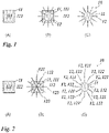
- the multi-layer body 10 comprises a first layer 11, which is designed as a metal layer, for example made of aluminum, and a second layer 12, which is designed as a colored etching resist.
- a first layer 11 which is designed as a metal layer, for example made of aluminum
- a second layer 12 which is designed as a colored etching resist.
- aluminum copper, silver or chrome are also suitable, as are a wide variety of metal alloys.
- the first layer 11 is produced, which can be done, for example, by vapor deposition onto a substrate (not shown).
- the vapor deposition is preferably carried out in a vacuum by thermal vaporization, by means of electron beam vaporization or also by means of sputtering.
- the layer thickness of the first layer 11 is preferably 5 nm to 100 nm, more preferably 15 nm to 40 nm.
- the first vapor-deposited layer can then be partially removed using known methods, for example by partially applying an etch resist after the vapor deposition and subsequent etching including removal of the etch resist; by the partial application of a wash lacquer before the vapor deposition and washing off (lift-off) after the vapor deposition or by the partial application of a photoresist after the vapor deposition and subsequent exposure and subsequent Removal of the exposed or unexposed parts of the photoresist depending on the type (positive, negative) of the photoresist.
- the substrate is not vapour-deposited over the entire surface, the layer 11 is rather produced partially, so that it is present in a first area 111 and is not present in a second area 112 .
- Various methods are known for this, such as shielding by means of a moving mask or pressure of an oil, which prevents the deposition of the metal layer in the vapor deposition process.
- ODD optically variable device
- the first layer 11 does not have to be continuous, as shown, but can be structured as desired and have any shape.
- the second layer 12, here in the form of a radial pattern is printed onto the first layer.
- the printing technique used is preferably intaglio printing, flexographic printing, offset printing, screen printing or digital printing, in particular ink jet printing.
- the second layer 12 extends both into the region 111 covered by the first layer 11, but does not cover it completely, and into the region 112 not covered by the first layer 11. If a replicated diffractive structure is present, printing takes place preferably in register with this structure, with tolerances of +/- 1 mm, preferably +/- 0.5 mm, depending on the printing process.
- the lacquer used to print the second layer 12 is an etching resist, ie resistant to an etchant which can dissolve the metal of the first layer 11 . If aluminum is used for the first layer, this etchant can be caustic soda, for example.
- a lacquer based on PVC/PVAc (polyvinyl acetate) copolymer, for example, is then suitable as an etching resist.
- the paint also contains dyes, pigments, in particular colored or achromatic pigments or effect pigments, thin-film layer systems or cholesteric liquid crystals or nanoparticles, so that it produces an optically visible effect.
- the etching is then preferably carried out at a concentration of 0.1% to 5%, an etchant temperature of 15° C. to 75° C. over a period of 5 seconds to 100 seconds.
- a suitable etching resist is, for example, a lacquer based on PVC/PVAc (polyvinyl acetate) copolymer, which is printed in a layer thickness of preferably 0.1 ⁇ m to 10 ⁇ m.
- the first layer 11 dissolves in the areas not covered by the second layer.
- a rinsing process for example with water, and a drying step can also follow the etching.
- 1c shows the resulting multi-layer body 10 from the side opposite the pressure side. It can be seen that the structures of the first layer 11 and second layer 12 seamlessly merge into one another, ie are arranged with register accuracy. This side is also the typical viewing side of the multi-layer body 10. If a replicated diffractive structure is present, the first layer 11 acts as a reflection layer, so that the diffractive structure in the region of the first layer 11 is particularly clearly visible. An additional coating with an adhesive layer (not shown) can completely erase the diffractive structure in the area 111 not covered by the first layer 11 if the adhesive layer has a similar refractive index (e.g. about 1.5) to the replication layer and therefore no optically effective boundary layer is formed between the adhesive layer and the replication layer.
- a similar refractive index e.g. about 1.5
- the adhesive layer serves to apply the multi-layer body 10 to a substrate, for example a bank note.
- the color can be designed to be largely transparent or translucent, so that the underlying substrate can be seen, but a largely opaque design is also possible.
- a metal layer as the first layer 11
- a plurality of adjacent color layers which are printed onto the substrate.
- Suitable resists for this are, for example, photoresists such as AZ 1518 from AZ Electronic Materials.
- the second layer 12 is then preferably a protective lacquer, for example a transparent or opaque lacquer with a UV blocker. Benzophenone derivatives or highly disperse titanium dioxide are particularly suitable for this.
- the second layer 12 is then preferably printed so that it overlaps with the boundary areas of the colored layers of the first layer 11 .
- a preferred exposure dose of 10 mJ/cm 2 to 500 mJ/cm 2 and etching with e.g. 0.3% NaOH at a preferred temperature of about 50°C for a time of preferably 10 seconds to 30 seconds then only the color components of the first layer 11 remain where they were covered by the second layer 12 and thus form a multicolored decoration.
- the second layer 12 in the form of guilloche lines the finished multi-layer body shows 10 guilloche lines in which color transitions show, ie a so-called iris print.
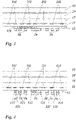
- the inside 2 Multi-layer body 10 shown is analogous to 1 produced.
- the second layer 12 is formed as a layer system by printing two differently colored lacquers 121, 122.
- the two lacquers 121, 122 can overlap in some areas and are preferably printed in register with a tolerance of preferably less than 0.5 mm and particularly preferably less than 0.2 mm.
- the result is the multi-layer body 10 according to Figure 2c .
- FIGS. 3 to 5 show the manufacturing steps of an alternative multi-layer body 10, which, however, corresponds to the basic structure in 2 shown.
- the essential difference lies in the fact that the second layer 12 is not already printed on in a structured manner in this case, but is first applied over the entire area or at least in large areas and is then structured.
- a release layer 14 and a replication layer 15 made of, for example, a thermoplastic material or a radiation-curable or temperature-curable replication lacquer are first applied to a carrier layer 13 made of polyester, in particular PET, with these layers in turn being able to consist of several layers.
- Diffractive structures 151 are then molded into the replication layer 15, for example by embossing with a metallic embossing tool.
- HRI High Refractive Index
- the second layer 12 is then applied to the first layer 11 over the entire surface or at least in large areas, which in turn consists of two differently colored lacquers 121, 122 which adjoin one another.
- the lacquers 121, 122 are UV-sensitive photoresists such as AZ 1518 from AZ Electronic Materials based on phenolic resin/diazoquinone.
- a mask layer 16 is then partially printed onto the second layer 12 .
- the mask layer 16 serves at the same time as an etching and protective lacquer.
- an etching resist lacquer for example based on PVC/PVAc (polyvinyl acetate) copolymer, can be provided with, for example, UV-absorbing titanium dioxide particles or other UV blockers.
- Exposure to UV light then takes place from the side of the mask layer 16 .
- the exposure preferably takes place at a wavelength of 365 nm with a dose of 25 mJ/cm 2 to 500 mJ/cm 2 .
- NaOH is suitable for this purpose, for example, in a preferred concentration of 0.05% to 2.5%, which preferably acts on the intermediate product for a period of 2 seconds to 60 seconds at a temperature of 20° C. to 65° C.
- the photoresist 121, 122 of the layer 12 was exposed during the UV irradiation and therefore now dissolves in the developer bath. You get that in 4 shown intermediate. However, this is not isolated. Rather, the etching process is continued, the HRI layer 11 now being attacked where it is not protected by the remaining layer 12 .
- the lacquers 121, 122 thus act here at the same time as an etching resist.
- the in figure 5 illustrated finished multi-layer body 10.
- An adhesive layer can also be applied to this, which fills the exposed diffractive structures 151 where they are not covered by the first layer 11. The diffractive structures 151 are then only visible where the HRI material of the first layer 11 acts as a reflection layer.
- FIG. 6 another multi-layer body 10 is shown. Layers 11 and 12 are applied in the same way as in 1 illustrated embodiment. A further transparent HRI layer 17 is then applied over the entire surface, so that a diffractive element 18 that is not covered by the first layer 11 becomes visible.
- Diffractive structures can thus be seen in the opaque metallic areas of the first layer 11 and in the areas of the transparent HRI layer 17, but typically not in the printed areas of the second layer 12, because the diffractive structures are printed directly onto the diffractive structures by the color coating of the second layer 12 are extinguished because the colored lacquer preferably has a similar refractive index (about 1.5) as the replication layer and therefore no optically effective boundary layer is formed between colored lacquer and replication layer.
- the refractive indices of the two adjacent layers should preferably not differ from one another by more than 0.1.
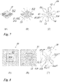
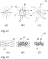
- the embodiment according to Fig. 7a-c again corresponds to the exemplary embodiment 1 .
- the only difference is that for the first Layer 11 two different metals 113, 114, such as Al and Cu are used.
- the two metals 113, 114 can be spatially separate, adjacent or partially overlapping.
- Figure 7b again shows how the second layer 12 is printed onto the first layer 11 viewed from the print side.
- Figure 7c shows the finished multi-layer body viewed from the metal side. Due to the opaque metal layers, the print of layer 12 under the metal areas of layer 11 is not visible.
- the first layer 11 can be structured in two steps, since, for example, different etching agents have to be used for the two metals or metal alloys used. If Al and Cu are used for the first layer 11, these are NaOH and FeCl 3 , for example. However, since the same printed mask is used for structuring, namely the second layer 12, the transitions between the two metals 113, 114 of the first layer 11 take place in perfect register, i.e. in the exact position relative to the printing of the second layer 12.
- the embodiment after 8 again corresponds to the exemplary embodiment 1 .
- only one more transparent HRI layer 17 is applied.
- an opaque metal 113 for example aluminum
- the HRI layer 17 made of ZnS or TiO 2 is applied, which can also be done by vapor deposition or sputtering, so that a layer arrangement according to FIG Figure 8a present.
- the HRI layer 17 can also be present only partially, bordering on the metal layer 113, or at least partially overlapping it.
- the metal layer 113 and the HRI layer 17 together form the first layer 11.
- a red color layer is overprinted as the second layer 12, so that the situation according to FIG Figure 8b results. Viewing is from the print side.
- the areas of the two reflection layers 113, 17 that are not overprinted are removed, possibly also in two process steps with chemicals that are matched to the layers to be removed, for example two different lyes.
- NaOH can be used to remove the aluminum fractions under the conditions described
- NaOH or Na 2 CO 3 is preferably also used to remove an HRI layer made of ZnS at a temperature of 20° C. to 60° C. for a period of 5 seconds to 60 seconds used.
- the finished multi-layer body is in Figure 8c seen from the side of the first layer 11.
- the effect of the diffractive structures in the substrate can also be seen in the non-metallic areas in which the HRI layer 17 is present, while at the same time the color print of the second layer 12 can be seen because the HRI layer is still between the printed and the diffractive structures 17 is arranged as an optical boundary layer.
- the colored lacquer can be made transparent, translucent or also largely opaque.
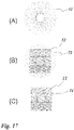
- the manufacturing process includes a first step in which the finely structured first layer 11 according to Figure 9a is produced.
- Correspondingly finely structured metal layers can be produced, for example, in the following way: by structuring a photoresist layer using high-resolution mask exposure, which is then in turn used to structure the metal layer, or by using a process for tolerance-free partial metallization, as is known, for example, from WO 2006/084685 A2 is known.
- the layer 11 consists of a fine grid, which consists, for example, of a microscopically fine text.
- the colored printing of the second layer 12 is then carried out according to FIG Figure 9b .
- the second layer 12 is a comparatively coarsely structured motif in the form of the large number "50".
- the second layer 12 can also be structured very finely.
- the colored print of layer 12 serves as a mask for removing the first layer 11 in register, so that the in 9c shown multi-layer body 10 is obtained. This is done analogously to the etching process already described.
- first layer 11 and second layer 12 are, for example, finely structured line grids, superposition effects occur depending on their relative position to one another, and the structure that is finally created is a finely structured superimposition structure of the first layer 11 and second layer 12.
- the overlay structure can produce a desired moiré effect, for example.
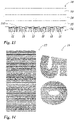
- the fine structuring of the first layer 11 can, for example, also be designed as a guilloche pattern made up of a large number of fine lines, preferably as a metallic reflection layer in combination with diffractive structures, for example with a KINEGRAM® , like this Figure 17A indicates.
- the colored printing of the second layer 12 is then carried out according to FIG Figure 17B .
- the colored print can have several differently colored areas, for example in the form of a national flag (as shown here) and/or a geographical contour of a country or in the form of a coat of arms or another multicolored motif.
- the colored print of layer 12 serves as a mask for removing the first layer 11 with precise register, so that the in Figure 17C shown multi-layer body 10 is obtained. This is done analogously to the etching process already described.
- the in 17 shown embodiment recognizes the viewer as counterfeit-proof and independent Characteristics that the finely structured lines are only present in the colored areas and the finely structured lines recognizable in one colored area continue in register in an adjacent further colored area.
- the fine structuring of the first layer 11 can also be implemented, for example, as a guilloche pattern made up of a large number of fine lines, preferably as a metallic reflection layer in combination with optical-diffraction structures, for example with a KINEGRAM® , like this 18A indicates.
- the second layer 12 is then printed according to FIG Figure 18B .
- a colorless, preferably transparent etching resist with a UV absorber is used.
- This etch resist should then fulfill a dual function: on the one hand, the etch resist is used for further substructuring of the finely structured first layer 11 by means of etching and, on the other hand, later as an exposure mask for structuring a color area.
- the fine structure of the first layer 11 is removed by etching in the areas in which the etching resist is not provided.
- a colored photoresist is then printed on, which covers at least the area that is not covered by the colorless etching resist.
- the photoresist can also overlap with the etch resist.
- the colored photoresist is cured in those areas that do not have a transparent etch resist and can register in the remaining areas with the etch resist and the areas protected and defined by the etch resist Areas of the finely structured first layer 11 are removed.
- the viewer recognizes as forgery-proof and independent features that the fine structures of the first layer 11 are only present in the colorless areas and end in register with the colored area of the photoresist and that the fine structures of the first layer 11 are practically "above the colored Across area" continue in register in an adjacent transparent area.
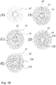
- the Figures 10 to 13 show the manufacturing steps of an alternative multi-layer body 10, which, however, corresponds to the basic structure in 9 shown.
- the essential difference lies in the fact that the second layer 12 is not already printed on in a structured manner in this case, but is first applied over the entire area or at least in large areas and is then structured.
- a release layer 14 and a replication layer 15 are first applied to a carrier layer 13 made of polyester or PET. Diffractive structures 151 are then molded into the replication layer 15 .
- the first layer 11 is now applied to the replication layer 15, which in this case is present as a finely structured metal layer, for example in the form of a grid.
- the resists 121, 122 are UV-sensitive colored photoresists.
- a mask layer 16 is then partially printed onto the second layer 12, so that the in 12 intermediate product shown is obtained.
- the mask layer 16 can have the form of a further grid.
- the mask layer 16 serves at the same time as an etching and protective lacquer.
- an etching resist can be provided with UV-absorbing titanium dioxide particles or other UV blockers, for example. Exposure to UV light then takes place from the side of the mask layer 16 .
- the exposure parameters and lacquers used correspond to those already described above.
- a film mask can also be used, which is only in contact with the layers 121 and 122 during the exposure process and is then removed again.
- first layer 11 and the second layer 12 Screenings of the first layer 11 and the second layer 12 are in 14 shown.
- other structures such as point grids, are of course also possible.
- the first layer 11 and/or the second layer 12 can be provided with a further grid of diffractive structures on the respective replication layer of the first and/or second layer second layer 11, 12, but also a further, additional overlay with the or the diffractive grids of the first and / or second layer or their optically variable effects.
- the overlay effects can be very different, depending on how similar or different the screen rulings and/or screen shapes of the screens involved in the overlay are.
- the viewing angle and/or illumination angle dependency of the diffractive raster can lead to surprising optical effects with this lead to complex superposition.
- first layer 11 a partial reflection layer made of opaque metal or transparent HRI material
- second layer 12 a print (second layer 12) is applied.
- the print of the second layer 12 serves as a mask layer, for example analogously to an etching resist print, for further structuring of the partial metal layer 11.
- a print (second layer 12) is first introduced into the pre-material, in which a diffractive structure (not shown) is then molded (see Figure 15a ).
- a first partial metal area (first layer 11) is produced, as in Figure 15b shown.
- the print already present in the starting material is used as an exposure mask for a photoresist layer applied thereto in order to structure the first layer 11 in perfect register for printing the second layer 12 .
- the materials and process parameters used correspond to those already described above.
- the second layer 12 is thus generated completely independently of the first layer 11 in terms of time and place.
- the second layer 12 can also be arranged, for example, on the rear side of the substrate, which is not shown, and the first layer 11 on its front side.
- the second layer 12 could be removed for specific purposes when it has served its purpose as a structuring aid for the first layer 11.
- FIG. 16 shows a multi-layer body 10.
- first the first layer 11 is produced as a metal layer with a recessed lettering 19 .
- the second layer 12 is, as in Figure 16b shown, printed as a wavy patterned lacquer layer on the first layer 11 and then serves as an etching resist mask for further structuring of the first layer 11 in a lye bath. After etching you get the in Figure 16c Multi-layer body 10 shown, in which the colored lines of the second layer 12 continue in the area of the recessed lettering in perfect register with the remaining metallic lines of the first layer 11 outside of the lettering 19.
- the line widths do not have to be constant, but can also be modulated, which results in different local area densities of the grid, which form additional information.
- the line widths are preferably from 25 ⁇ m to 150 ⁇ m.
- the screen width can also be modulated and is preferably less than 300 ⁇ m and preferably less than 200 ⁇ m, and preferably more than 25 ⁇ m.
Landscapes
- Engineering & Computer Science (AREA)
- Manufacturing & Machinery (AREA)
- Chemical & Material Sciences (AREA)
- Chemical Kinetics & Catalysis (AREA)
- General Chemical & Material Sciences (AREA)
- Accounting & Taxation (AREA)
- Finance (AREA)
- Business, Economics & Management (AREA)
- Crystallography & Structural Chemistry (AREA)
- Laminated Bodies (AREA)
- Credit Cards Or The Like (AREA)
- Application Of Or Painting With Fluid Materials (AREA)
- Diffracting Gratings Or Hologram Optical Elements (AREA)
- Holo Graphy (AREA)
- Floor Finish (AREA)
- Burglar Alarm Systems (AREA)
- Photometry And Measurement Of Optical Pulse Characteristics (AREA)
- Feeding, Discharge, Calcimining, Fusing, And Gas-Generation Devices (AREA)
- Air Bags (AREA)
- Prostheses (AREA)
Priority Applications (2)
| Application Number | Priority Date | Filing Date | Title |
|---|---|---|---|
| PL14805273.1T PL3074239T5 (pl) | 2013-11-29 | 2014-11-28 | Korpus wielowarstwowy jako element zabezpieczający i sposób jego wytwarzania |
| RS20190222A RS58357B2 (sr) | 2013-11-29 | 2014-11-28 | Višeslojno telo kao sigurnosni element i postupak za njegovu izradu |
Applications Claiming Priority (2)
| Application Number | Priority Date | Filing Date | Title |
|---|---|---|---|
| DE102013113283.9A DE102013113283A1 (de) | 2013-11-29 | 2013-11-29 | Mehrschichtkörper und Verfahren zu dessen Herstellung |
| PCT/EP2014/075928 WO2015079017A1 (de) | 2013-11-29 | 2014-11-28 | Mehrschichtkörper und verfahren zu dessen herstellung |
Publications (3)
| Publication Number | Publication Date |
|---|---|
| EP3074239A1 EP3074239A1 (de) | 2016-10-05 |
| EP3074239B1 EP3074239B1 (de) | 2018-12-19 |
| EP3074239B2 true EP3074239B2 (de) | 2022-04-13 |
Family
ID=51999431
Family Applications (1)
| Application Number | Title | Priority Date | Filing Date |
|---|---|---|---|
| EP14805273.1A Active EP3074239B2 (de) | 2013-11-29 | 2014-11-28 | Mehrschichtkörper als sicherheitselement und verfahren zu dessen herstellung |
Country Status (11)
| Country | Link |
|---|---|
| US (2) | US9956807B2 (pl) |
| EP (1) | EP3074239B2 (pl) |
| JP (1) | JP6634659B2 (pl) |
| CN (1) | CN105793060B (pl) |
| CA (1) | CA2930911C (pl) |
| DE (1) | DE102013113283A1 (pl) |
| ES (1) | ES2711547T5 (pl) |
| PL (1) | PL3074239T5 (pl) |
| RS (1) | RS58357B2 (pl) |
| TR (1) | TR201902966T4 (pl) |
| WO (1) | WO2015079017A1 (pl) |
Families Citing this family (11)
| Publication number | Priority date | Publication date | Assignee | Title |
|---|---|---|---|---|
| US6644309B2 (en) | 2001-01-12 | 2003-11-11 | Becton, Dickinson And Company | Medicament respiratory delivery device and method |
| DE102015104416A1 (de) * | 2015-03-24 | 2016-09-29 | Leonhard Kurz Stiftung & Co. Kg | Mehrschichtkörper und Verfahren zu dessen Herstellung |
| DE102015015991A1 (de) * | 2015-12-10 | 2017-06-14 | Giesecke & Devrient Gmbh | Sicherheitselement mit Linsenrasterbild |
| FR3057205B1 (fr) * | 2016-10-10 | 2020-10-16 | Arjowiggins Security | Procede de fabrication d'un element de securite |
| DE102017106721A1 (de) * | 2017-03-29 | 2018-10-04 | Leonhard Kurz Stiftung & Co. Kg | Verfahren zum Herstellen einer Mehrschichtfolie und eine Mehrschichtfolie sowie ein Sicherheitselement und ein Sicherheitsdokument |
| US11167581B2 (en) | 2018-04-06 | 2021-11-09 | Proof Authentication Corporation | Authentication hologram |
| DE102018003030A1 (de) * | 2018-04-13 | 2019-10-17 | Giesecke+Devrient Currency Technology Gmbh | Sicherheitselement, Verfahren zum Herstellen desselben und mit dem Sicherheitselement ausgestatteter Datenträger |
| CA3007268C (en) * | 2018-06-05 | 2023-12-12 | Canadian Bank Note Company, Limited | Method for making a security document comprising a thermosplastic substrate and uv-cured image and security document formed thereby |
| EP4309913A1 (en) | 2019-05-20 | 2024-01-24 | Crane & Co., Inc. | A security device including nanoparticles to tune index of refraction of layers of a polymeric matrix to optimize microoptic focus |
| CN114689097B (zh) * | 2020-06-18 | 2023-11-24 | 中国科学院苏州生物医学工程技术研究所 | 一种超声旋转编码器的传感部件 |
| EP4271572A1 (en) * | 2020-12-29 | 2023-11-08 | EPTAINKS S.p.A. | Security element for documents, particularly banknotes, and method for its production |
Citations (10)
| Publication number | Priority date | Publication date | Assignee | Title |
|---|---|---|---|---|
| WO1997023357A1 (de) † | 1995-12-22 | 1997-07-03 | Giesecke & Devrient Gmbh | Sicherheitsdokument mit einem sicherheitselement und verfahren zu dessen herstellung |
| DE10226116A1 (de) † | 2001-12-21 | 2003-07-03 | Giesecke & Devrient Gmbh | Sicherheitselement und Verfahren zu seiner Herstellung |
| US7029757B1 (en) † | 1999-07-30 | 2006-04-18 | Gaj Developpement Sas | Method for producing security marks and security marks |
| EP1747905A2 (de) † | 2005-07-25 | 2007-01-31 | Giesecke & Devrient GmbH | Sicherheitselement und Verfahren zu seiner Herstellung |
| WO2008120080A2 (en) † | 2007-03-30 | 2008-10-09 | Medichem, S.A. | An improved process for the synthesis of solifenacin |
| DE102008013073A1 (de) † | 2008-03-06 | 2009-09-10 | Leonhard Kurz Stiftung & Co. Kg | Verfahren zur Herstellung eines Folienkörpers |
| WO2010015381A2 (de) † | 2008-08-05 | 2010-02-11 | Giesecke & Devrient Gmbh | Verfahren zur herstellung von sicherheitselementen mit zueinander gepasserten motiven |
| WO2010015384A2 (de) † | 2008-08-05 | 2010-02-11 | Giesecke & Devrient Gmbh | Verfahren zur herstellung von sicherheitselementen mit gepasserten motivschichten |
| WO2011006634A2 (de) † | 2009-07-17 | 2011-01-20 | Leonhard Kurz Stiftung & Co. Kg | Verfahren zur herstellung eines mehrschichtkörpers sowie mehrschichtkörper |
| WO2014207165A1 (de) † | 2013-06-28 | 2014-12-31 | Leonhard Kurz Stiftung & Co. Kg | Verfahren zur herstellung eines mehrschichtkörpers sowie mehrschichtkörper |
Family Cites Families (18)
| Publication number | Priority date | Publication date | Assignee | Title |
|---|---|---|---|---|
| DE10333255B3 (de) | 2003-07-21 | 2005-01-13 | Leonhard Kurz Gmbh & Co. Kg | Verfahren zur Erzeugung eines Flächenmusters hoher Auflösung |
| EP1634722B8 (de) * | 2004-09-09 | 2009-10-07 | Alcan Technology & Management Ltd. | Gegenstand mit fälschungssicherer Bedruckung |
| DE102005006231B4 (de) | 2005-02-10 | 2007-09-20 | Ovd Kinegram Ag | Verfahren zur Herstellung eines Mehrschichtkörpers |
| WO2006090417A1 (en) * | 2005-02-28 | 2006-08-31 | Stmicroelectronics S.R.L. | Method for realising a nanometric circuit architecture between standard electronic components and semiconductor device obtained with said method |
| ITMI20051944A1 (it) * | 2005-10-14 | 2007-04-15 | Fabriano Securities Srl | Elemento di sicurezza per banconote o documenti rappresentanti un valore |
| JP5204959B2 (ja) * | 2006-06-26 | 2013-06-05 | 株式会社半導体エネルギー研究所 | 半導体装置の作製方法 |
| DE102006037431A1 (de) | 2006-08-09 | 2008-04-17 | Ovd Kinegram Ag | Verfahren zur Herstellung eines Mehrschichtkörpers sowie Mehrschichtkörper |
| CA2613830A1 (en) * | 2006-12-15 | 2008-06-15 | Alberto Argoitia | An article with micro indicia security enhancement |
| DE102007039996B4 (de) * | 2007-02-07 | 2020-09-24 | Leonhard Kurz Stiftung & Co. Kg | Sicherheitselement für ein Sicherheitsdokument und Verfahren zu seiner Herstellung |
| DE102007007914A1 (de) | 2007-02-14 | 2008-08-21 | Giesecke & Devrient Gmbh | Prägelack für mikrooptische Sicherheitselemente |
| JP4924088B2 (ja) * | 2007-02-22 | 2012-04-25 | 大日本印刷株式会社 | 真偽判定用媒体およびそれを有する物品、真偽判定用媒体ラベル、真偽判定用媒体転写シートならびに真偽判定用媒体転写箔 |
| GB2456500B (en) * | 2007-10-23 | 2011-12-28 | Rue De Int Ltd | Improvements in security elements |
| DE102008027952A1 (de) | 2008-06-12 | 2009-12-17 | Giesecke & Devrient Gmbh | Sicherheitselement mit gerasterter Schicht aus Rasterelementen |
| GB2464496B (en) | 2008-10-16 | 2013-10-09 | Rue De Int Ltd | Improvements in printed security features |
| MX2011013708A (es) | 2009-06-18 | 2012-02-22 | Toppan Printing Co Ltd | Elemento optico y metodo para fabricar el mismo. |
| FR2948216B1 (fr) * | 2009-07-17 | 2011-11-25 | Arjowiggins Security | Element de securite a effet de parallaxe |
| JP2012189935A (ja) * | 2011-03-14 | 2012-10-04 | Toppan Printing Co Ltd | 光学素子 |
| CN102368381A (zh) * | 2011-10-27 | 2012-03-07 | 深圳市华星光电技术有限公司 | 改善液晶面板的充电的方法与电路 |
-
2013
- 2013-11-29 DE DE102013113283.9A patent/DE102013113283A1/de not_active Withdrawn
-
2014
- 2014-11-28 JP JP2016534897A patent/JP6634659B2/ja active Active
- 2014-11-28 EP EP14805273.1A patent/EP3074239B2/de active Active
- 2014-11-28 WO PCT/EP2014/075928 patent/WO2015079017A1/de not_active Ceased
- 2014-11-28 RS RS20190222A patent/RS58357B2/sr unknown
- 2014-11-28 PL PL14805273.1T patent/PL3074239T5/pl unknown
- 2014-11-28 TR TR2019/02966T patent/TR201902966T4/tr unknown
- 2014-11-28 CA CA2930911A patent/CA2930911C/en active Active
- 2014-11-28 US US15/038,874 patent/US9956807B2/en active Active
- 2014-11-28 ES ES14805273T patent/ES2711547T5/es active Active
- 2014-11-28 CN CN201480065028.1A patent/CN105793060B/zh active Active
-
2018
- 2018-04-03 US US15/944,262 patent/US10850551B2/en active Active
Patent Citations (10)
| Publication number | Priority date | Publication date | Assignee | Title |
|---|---|---|---|---|
| WO1997023357A1 (de) † | 1995-12-22 | 1997-07-03 | Giesecke & Devrient Gmbh | Sicherheitsdokument mit einem sicherheitselement und verfahren zu dessen herstellung |
| US7029757B1 (en) † | 1999-07-30 | 2006-04-18 | Gaj Developpement Sas | Method for producing security marks and security marks |
| DE10226116A1 (de) † | 2001-12-21 | 2003-07-03 | Giesecke & Devrient Gmbh | Sicherheitselement und Verfahren zu seiner Herstellung |
| EP1747905A2 (de) † | 2005-07-25 | 2007-01-31 | Giesecke & Devrient GmbH | Sicherheitselement und Verfahren zu seiner Herstellung |
| WO2008120080A2 (en) † | 2007-03-30 | 2008-10-09 | Medichem, S.A. | An improved process for the synthesis of solifenacin |
| DE102008013073A1 (de) † | 2008-03-06 | 2009-09-10 | Leonhard Kurz Stiftung & Co. Kg | Verfahren zur Herstellung eines Folienkörpers |
| WO2010015381A2 (de) † | 2008-08-05 | 2010-02-11 | Giesecke & Devrient Gmbh | Verfahren zur herstellung von sicherheitselementen mit zueinander gepasserten motiven |
| WO2010015384A2 (de) † | 2008-08-05 | 2010-02-11 | Giesecke & Devrient Gmbh | Verfahren zur herstellung von sicherheitselementen mit gepasserten motivschichten |
| WO2011006634A2 (de) † | 2009-07-17 | 2011-01-20 | Leonhard Kurz Stiftung & Co. Kg | Verfahren zur herstellung eines mehrschichtkörpers sowie mehrschichtkörper |
| WO2014207165A1 (de) † | 2013-06-28 | 2014-12-31 | Leonhard Kurz Stiftung & Co. Kg | Verfahren zur herstellung eines mehrschichtkörpers sowie mehrschichtkörper |
Also Published As
| Publication number | Publication date |
|---|---|
| US20170028765A1 (en) | 2017-02-02 |
| JP2017500607A (ja) | 2017-01-05 |
| ES2711547T5 (es) | 2022-07-12 |
| US10850551B2 (en) | 2020-12-01 |
| US9956807B2 (en) | 2018-05-01 |
| CA2930911C (en) | 2021-12-28 |
| EP3074239B1 (de) | 2018-12-19 |
| EP3074239A1 (de) | 2016-10-05 |
| PL3074239T5 (pl) | 2022-07-18 |
| PL3074239T3 (pl) | 2019-06-28 |
| WO2015079017A1 (de) | 2015-06-04 |
| JP6634659B2 (ja) | 2020-01-22 |
| DE102013113283A1 (de) | 2015-06-03 |
| CA2930911A1 (en) | 2015-06-04 |
| CN105793060B (zh) | 2017-10-24 |
| TR201902966T4 (tr) | 2019-03-21 |
| US20180290480A1 (en) | 2018-10-11 |
| RS58357B1 (sr) | 2019-03-29 |
| ES2711547T3 (es) | 2019-05-06 |
| RS58357B2 (sr) | 2022-06-30 |
| CN105793060A (zh) | 2016-07-20 |
Similar Documents
| Publication | Publication Date | Title |
|---|---|---|
| EP3074239B2 (de) | Mehrschichtkörper als sicherheitselement und verfahren zu dessen herstellung | |
| DE102014106340B4 (de) | Mehrschichtkörper und Verfahren zu dessen Herstellung sowie Sicherheitsdokument | |
| DE102009032697B3 (de) | Mehrschichtkörper | |
| EP2860041B1 (de) | Verfahren zur Herstellung eines Mehrschichtkörpers sowie Mehrschichtkörper | |
| DE102018103236A1 (de) | Sicherheitselement und Verfahren zur Herstellung eines Sicherheitselements | |
| EP3013598B2 (de) | Verfahren zur herstellung eines mehrschichtkörpers | |
| EP3288773B1 (de) | Verfahren zum herstellen eines mehrschichtkörpers | |
| DE102015015991A1 (de) | Sicherheitselement mit Linsenrasterbild | |
| EP3274183B1 (de) | Mehrschichtkörper und verfahren zu dessen herstellung | |
| EP1599344B1 (de) | Sicherheitselement | |
| EP3606766B1 (de) | Sicherheitselement und herstellungsverfahren hierfür | |
| DE102023128009A1 (de) | Verfahren zur Herstellung eines Mehrschichtkörpers sowie Mehrschichtkörper | |
| EP3486092A1 (de) | Verfahren zum herstellen eines sicherheitselementes |
Legal Events
| Date | Code | Title | Description |
|---|---|---|---|
| PUAI | Public reference made under article 153(3) epc to a published international application that has entered the european phase |
Free format text: ORIGINAL CODE: 0009012 |
|
| 17P | Request for examination filed |
Effective date: 20160628 |
|
| AK | Designated contracting states |
Kind code of ref document: A1 Designated state(s): AL AT BE BG CH CY CZ DE DK EE ES FI FR GB GR HR HU IE IS IT LI LT LU LV MC MK MT NL NO PL PT RO RS SE SI SK SM TR |
|
| AX | Request for extension of the european patent |
Extension state: BA ME |
|
| RIN1 | Information on inventor provided before grant (corrected) |
Inventor name: FOERSTER, KARIN Inventor name: STAUB, RENE Inventor name: SPIESS, ROUVEN Inventor name: KRAEMER, PATRICK Inventor name: BREHM, LUDWIG |
|
| REG | Reference to a national code |
Ref country code: FR Ref legal event code: EL |
|
| DAX | Request for extension of the european patent (deleted) | ||
| STAA | Information on the status of an ep patent application or granted ep patent |
Free format text: STATUS: EXAMINATION IS IN PROGRESS |
|
| 17Q | First examination report despatched |
Effective date: 20170919 |
|
| GRAP | Despatch of communication of intention to grant a patent |
Free format text: ORIGINAL CODE: EPIDOSNIGR1 |
|
| STAA | Information on the status of an ep patent application or granted ep patent |
Free format text: STATUS: GRANT OF PATENT IS INTENDED |
|
| INTG | Intention to grant announced |
Effective date: 20180706 |
|
| GRAS | Grant fee paid |
Free format text: ORIGINAL CODE: EPIDOSNIGR3 |
|
| GRAA | (expected) grant |
Free format text: ORIGINAL CODE: 0009210 |
|
| STAA | Information on the status of an ep patent application or granted ep patent |
Free format text: STATUS: THE PATENT HAS BEEN GRANTED |
|
| RIN1 | Information on inventor provided before grant (corrected) |
Inventor name: STAUB, RENE Inventor name: FOERSTER, KARIN Inventor name: KRAEMER, PATRICK Inventor name: SPIESS, ROUVEN Inventor name: BREHM, LUDWIG |
|
| AK | Designated contracting states |
Kind code of ref document: B1 Designated state(s): AL AT BE BG CH CY CZ DE DK EE ES FI FR GB GR HR HU IE IS IT LI LT LU LV MC MK MT NL NO PL PT RO RS SE SI SK SM TR |
|
| REG | Reference to a national code |
Ref country code: GB Ref legal event code: FG4D Free format text: NOT ENGLISH |
|
| REG | Reference to a national code |
Ref country code: CH Ref legal event code: EP |
|
| REG | Reference to a national code |
Ref country code: IE Ref legal event code: FG4D Free format text: LANGUAGE OF EP DOCUMENT: GERMAN |
|
| REG | Reference to a national code |
Ref country code: DE Ref legal event code: R096 Ref document number: 502014010416 Country of ref document: DE |
|
| REG | Reference to a national code |
Ref country code: CH Ref legal event code: NV Representative=s name: FIAMMENGHI-FIAMMENGHI, CH Ref country code: AT Ref legal event code: REF Ref document number: 1078276 Country of ref document: AT Kind code of ref document: T Effective date: 20190115 |
|
| REG | Reference to a national code |
Ref country code: NL Ref legal event code: FP |
|
| PG25 | Lapsed in a contracting state [announced via postgrant information from national office to epo] |
Ref country code: HR Free format text: LAPSE BECAUSE OF FAILURE TO SUBMIT A TRANSLATION OF THE DESCRIPTION OR TO PAY THE FEE WITHIN THE PRESCRIBED TIME-LIMIT Effective date: 20181219 Ref country code: NO Free format text: LAPSE BECAUSE OF FAILURE TO SUBMIT A TRANSLATION OF THE DESCRIPTION OR TO PAY THE FEE WITHIN THE PRESCRIBED TIME-LIMIT Effective date: 20190319 Ref country code: LT Free format text: LAPSE BECAUSE OF FAILURE TO SUBMIT A TRANSLATION OF THE DESCRIPTION OR TO PAY THE FEE WITHIN THE PRESCRIBED TIME-LIMIT Effective date: 20181219 Ref country code: LV Free format text: LAPSE BECAUSE OF FAILURE TO SUBMIT A TRANSLATION OF THE DESCRIPTION OR TO PAY THE FEE WITHIN THE PRESCRIBED TIME-LIMIT Effective date: 20181219 |
|
| REG | Reference to a national code |
Ref country code: ES Ref legal event code: FG2A Ref document number: 2711547 Country of ref document: ES Kind code of ref document: T3 Effective date: 20190506 |
|
| REG | Reference to a national code |
Ref country code: LT Ref legal event code: MG4D |
|
| PG25 | Lapsed in a contracting state [announced via postgrant information from national office to epo] |
Ref country code: AL Free format text: LAPSE BECAUSE OF FAILURE TO SUBMIT A TRANSLATION OF THE DESCRIPTION OR TO PAY THE FEE WITHIN THE PRESCRIBED TIME-LIMIT Effective date: 20181219 Ref country code: SE Free format text: LAPSE BECAUSE OF FAILURE TO SUBMIT A TRANSLATION OF THE DESCRIPTION OR TO PAY THE FEE WITHIN THE PRESCRIBED TIME-LIMIT Effective date: 20181219 |
|
| REG | Reference to a national code |
Ref country code: GR Ref legal event code: EP Ref document number: 20190400400 Country of ref document: GR Effective date: 20190509 |
|
| RAP2 | Party data changed (patent owner data changed or rights of a patent transferred) |
Owner name: LEONHARD KURZ STIFTUNG & CO. KG Owner name: OVD KINEGRAM AG |
|
| PG25 | Lapsed in a contracting state [announced via postgrant information from national office to epo] |
Ref country code: PT Free format text: LAPSE BECAUSE OF FAILURE TO SUBMIT A TRANSLATION OF THE DESCRIPTION OR TO PAY THE FEE WITHIN THE PRESCRIBED TIME-LIMIT Effective date: 20190419 Ref country code: CZ Free format text: LAPSE BECAUSE OF FAILURE TO SUBMIT A TRANSLATION OF THE DESCRIPTION OR TO PAY THE FEE WITHIN THE PRESCRIBED TIME-LIMIT Effective date: 20181219 |
|
| PG25 | Lapsed in a contracting state [announced via postgrant information from national office to epo] |
Ref country code: RO Free format text: LAPSE BECAUSE OF FAILURE TO SUBMIT A TRANSLATION OF THE DESCRIPTION OR TO PAY THE FEE WITHIN THE PRESCRIBED TIME-LIMIT Effective date: 20181219 Ref country code: IS Free format text: LAPSE BECAUSE OF FAILURE TO SUBMIT A TRANSLATION OF THE DESCRIPTION OR TO PAY THE FEE WITHIN THE PRESCRIBED TIME-LIMIT Effective date: 20190419 Ref country code: EE Free format text: LAPSE BECAUSE OF FAILURE TO SUBMIT A TRANSLATION OF THE DESCRIPTION OR TO PAY THE FEE WITHIN THE PRESCRIBED TIME-LIMIT Effective date: 20181219 Ref country code: SM Free format text: LAPSE BECAUSE OF FAILURE TO SUBMIT A TRANSLATION OF THE DESCRIPTION OR TO PAY THE FEE WITHIN THE PRESCRIBED TIME-LIMIT Effective date: 20181219 Ref country code: SK Free format text: LAPSE BECAUSE OF FAILURE TO SUBMIT A TRANSLATION OF THE DESCRIPTION OR TO PAY THE FEE WITHIN THE PRESCRIBED TIME-LIMIT Effective date: 20181219 |
|
| REG | Reference to a national code |
Ref country code: DE Ref legal event code: R026 Ref document number: 502014010416 Country of ref document: DE |
|
| PLBI | Opposition filed |
Free format text: ORIGINAL CODE: 0009260 |
|
| PLAX | Notice of opposition and request to file observation + time limit sent |
Free format text: ORIGINAL CODE: EPIDOSNOBS2 |
|
| 26 | Opposition filed |
Opponent name: GIESECKE+DEVRIENT CURRENCY TECHNOLOGY GMBH Effective date: 20190919 |
|
| PG25 | Lapsed in a contracting state [announced via postgrant information from national office to epo] |
Ref country code: DK Free format text: LAPSE BECAUSE OF FAILURE TO SUBMIT A TRANSLATION OF THE DESCRIPTION OR TO PAY THE FEE WITHIN THE PRESCRIBED TIME-LIMIT Effective date: 20181219 |
|
| PLBB | Reply of patent proprietor to notice(s) of opposition received |
Free format text: ORIGINAL CODE: EPIDOSNOBS3 |
|
| PG25 | Lapsed in a contracting state [announced via postgrant information from national office to epo] |
Ref country code: SI Free format text: LAPSE BECAUSE OF FAILURE TO SUBMIT A TRANSLATION OF THE DESCRIPTION OR TO PAY THE FEE WITHIN THE PRESCRIBED TIME-LIMIT Effective date: 20181219 |
|
| PG25 | Lapsed in a contracting state [announced via postgrant information from national office to epo] |
Ref country code: MC Free format text: LAPSE BECAUSE OF FAILURE TO SUBMIT A TRANSLATION OF THE DESCRIPTION OR TO PAY THE FEE WITHIN THE PRESCRIBED TIME-LIMIT Effective date: 20181219 Ref country code: LU Free format text: LAPSE BECAUSE OF NON-PAYMENT OF DUE FEES Effective date: 20191128 |
|
| REG | Reference to a national code |
Ref country code: BE Ref legal event code: MM Effective date: 20191130 |
|
| PG25 | Lapsed in a contracting state [announced via postgrant information from national office to epo] |
Ref country code: IE Free format text: LAPSE BECAUSE OF NON-PAYMENT OF DUE FEES Effective date: 20191128 |
|
| PG25 | Lapsed in a contracting state [announced via postgrant information from national office to epo] |
Ref country code: BE Free format text: LAPSE BECAUSE OF NON-PAYMENT OF DUE FEES Effective date: 20191130 |
|
| PLAB | Opposition data, opponent's data or that of the opponent's representative modified |
Free format text: ORIGINAL CODE: 0009299OPPO |
|
| R26 | Opposition filed (corrected) |
Opponent name: GIESECKE+DEVRIENT CURRENCY TECHNOLOGY GMBH Effective date: 20190919 |
|
| PG25 | Lapsed in a contracting state [announced via postgrant information from national office to epo] |
Ref country code: CY Free format text: LAPSE BECAUSE OF FAILURE TO SUBMIT A TRANSLATION OF THE DESCRIPTION OR TO PAY THE FEE WITHIN THE PRESCRIBED TIME-LIMIT Effective date: 20181219 |
|
| PG25 | Lapsed in a contracting state [announced via postgrant information from national office to epo] |
Ref country code: HU Free format text: LAPSE BECAUSE OF FAILURE TO SUBMIT A TRANSLATION OF THE DESCRIPTION OR TO PAY THE FEE WITHIN THE PRESCRIBED TIME-LIMIT; INVALID AB INITIO Effective date: 20141128 Ref country code: MT Free format text: LAPSE BECAUSE OF FAILURE TO SUBMIT A TRANSLATION OF THE DESCRIPTION OR TO PAY THE FEE WITHIN THE PRESCRIBED TIME-LIMIT Effective date: 20181219 |
|
| APAH | Appeal reference modified |
Free format text: ORIGINAL CODE: EPIDOSCREFNO |
|
| APBM | Appeal reference recorded |
Free format text: ORIGINAL CODE: EPIDOSNREFNO |
|
| APBP | Date of receipt of notice of appeal recorded |
Free format text: ORIGINAL CODE: EPIDOSNNOA2O |
|
| APBU | Appeal procedure closed |
Free format text: ORIGINAL CODE: EPIDOSNNOA9O |
|
| REG | Reference to a national code |
Ref country code: CH Ref legal event code: PK Free format text: BERICHTIGUNGEN |
|
| RIN2 | Information on inventor provided after grant (corrected) |
Inventor name: FOERSTER, KARIN Inventor name: SPIESS, ROUVEN Inventor name: KRAEMER, PATRICK Inventor name: BREHM, LUDWIG Inventor name: STAUB, RENE |
|
| PUAH | Patent maintained in amended form |
Free format text: ORIGINAL CODE: 0009272 |
|
| STAA | Information on the status of an ep patent application or granted ep patent |
Free format text: STATUS: PATENT MAINTAINED AS AMENDED |
|
| 27A | Patent maintained in amended form |
Effective date: 20220413 |
|
| AK | Designated contracting states |
Kind code of ref document: B2 Designated state(s): AL AT BE BG CH CY CZ DE DK EE ES FI FR GB GR HR HU IE IS IT LI LT LU LV MC MK MT NL NO PL PT RO RS SE SI SK SM TR |
|
| REG | Reference to a national code |
Ref country code: DE Ref legal event code: R102 Ref document number: 502014010416 Country of ref document: DE |
|
| REG | Reference to a national code |
Ref country code: NL Ref legal event code: FP |
|
| REG | Reference to a national code |
Ref country code: GR Ref legal event code: EP Ref document number: 20220400848 Country of ref document: GR Effective date: 20220509 |
|
| PG25 | Lapsed in a contracting state [announced via postgrant information from national office to epo] |
Ref country code: MK Free format text: LAPSE BECAUSE OF FAILURE TO SUBMIT A TRANSLATION OF THE DESCRIPTION OR TO PAY THE FEE WITHIN THE PRESCRIBED TIME-LIMIT Effective date: 20181219 |
|
| REG | Reference to a national code |
Ref country code: ES Ref legal event code: DC2A Ref document number: 2711547 Country of ref document: ES Kind code of ref document: T5 Effective date: 20220712 |
|
| REG | Reference to a national code |
Ref country code: CH Ref legal event code: U11 Free format text: ST27 STATUS EVENT CODE: U-0-0-U10-U11 (AS PROVIDED BY THE NATIONAL OFFICE) Effective date: 20251201 |
|
| PGFP | Annual fee paid to national office [announced via postgrant information from national office to epo] |
Ref country code: NL Payment date: 20251119 Year of fee payment: 12 |
|
| PGFP | Annual fee paid to national office [announced via postgrant information from national office to epo] |
Ref country code: DE Payment date: 20251121 Year of fee payment: 12 |
|
| PGFP | Annual fee paid to national office [announced via postgrant information from national office to epo] |
Ref country code: GB Payment date: 20251120 Year of fee payment: 12 |
|
| PGFP | Annual fee paid to national office [announced via postgrant information from national office to epo] |
Ref country code: AT Payment date: 20251117 Year of fee payment: 12 |
|
| PGFP | Annual fee paid to national office [announced via postgrant information from national office to epo] |
Ref country code: IT Payment date: 20251128 Year of fee payment: 12 Ref country code: FI Payment date: 20251118 Year of fee payment: 12 |
|
| PGFP | Annual fee paid to national office [announced via postgrant information from national office to epo] |
Ref country code: FR Payment date: 20251120 Year of fee payment: 12 |
|
| PGFP | Annual fee paid to national office [announced via postgrant information from national office to epo] |
Ref country code: TR Payment date: 20251124 Year of fee payment: 12 Ref country code: GR Payment date: 20251117 Year of fee payment: 12 |
|
| PGFP | Annual fee paid to national office [announced via postgrant information from national office to epo] |
Ref country code: CH Payment date: 20251201 Year of fee payment: 12 |
|
| PGFP | Annual fee paid to national office [announced via postgrant information from national office to epo] |
Ref country code: BG Payment date: 20251114 Year of fee payment: 12 Ref country code: PL Payment date: 20251009 Year of fee payment: 12 |
|
| PGFP | Annual fee paid to national office [announced via postgrant information from national office to epo] |
Ref country code: RS Payment date: 20251118 Year of fee payment: 12 |
|
| PGFP | Annual fee paid to national office [announced via postgrant information from national office to epo] |
Ref country code: ES Payment date: 20251216 Year of fee payment: 12 |