EP3069353B1 - An electrically conductive article containing shaped particles and methods of making same - Google Patents
An electrically conductive article containing shaped particles and methods of making same Download PDFInfo
- Publication number
- EP3069353B1 EP3069353B1 EP14803303.8A EP14803303A EP3069353B1 EP 3069353 B1 EP3069353 B1 EP 3069353B1 EP 14803303 A EP14803303 A EP 14803303A EP 3069353 B1 EP3069353 B1 EP 3069353B1
- Authority
- EP
- European Patent Office
- Prior art keywords
- electrically conductive
- shaped particles
- particles
- composite
- item
- Prior art date
- Legal status (The legal status is an assumption and is not a legal conclusion. Google has not performed a legal analysis and makes no representation as to the accuracy of the status listed.)
- Active
Links
- 239000002245 particle Substances 0.000 title claims description 415
- 238000000034 method Methods 0.000 title claims description 95
- 239000002131 composite material Substances 0.000 claims description 184
- 229920005989 resin Polymers 0.000 claims description 99
- 239000011347 resin Substances 0.000 claims description 99
- 238000009826 distribution Methods 0.000 claims description 64
- 229910052751 metal Inorganic materials 0.000 claims description 63
- 239000002184 metal Substances 0.000 claims description 63
- 239000000758 substrate Substances 0.000 claims description 38
- 238000012360 testing method Methods 0.000 claims description 32
- 238000000576 coating method Methods 0.000 claims description 31
- 239000011248 coating agent Substances 0.000 claims description 30
- 239000011231 conductive filler Substances 0.000 claims description 20
- 229910003460 diamond Inorganic materials 0.000 claims description 17
- 239000010432 diamond Substances 0.000 claims description 17
- PNEYBMLMFCGWSK-UHFFFAOYSA-N aluminium oxide Inorganic materials [O-2].[O-2].[O-2].[Al+3].[Al+3] PNEYBMLMFCGWSK-UHFFFAOYSA-N 0.000 claims description 15
- NIXOWILDQLNWCW-UHFFFAOYSA-N acrylic acid group Chemical group C(C=C)(=O)O NIXOWILDQLNWCW-UHFFFAOYSA-N 0.000 claims description 14
- BQCADISMDOOEFD-UHFFFAOYSA-N Silver Chemical compound [Ag] BQCADISMDOOEFD-UHFFFAOYSA-N 0.000 claims description 13
- 229910052709 silver Inorganic materials 0.000 claims description 13
- PCHJSUWPFVWCPO-UHFFFAOYSA-N gold Chemical compound [Au] PCHJSUWPFVWCPO-UHFFFAOYSA-N 0.000 claims description 12
- 229910052737 gold Inorganic materials 0.000 claims description 12
- 239000010931 gold Substances 0.000 claims description 12
- 229920001296 polysiloxane Polymers 0.000 claims description 12
- RYGMFSIKBFXOCR-UHFFFAOYSA-N Copper Chemical compound [Cu] RYGMFSIKBFXOCR-UHFFFAOYSA-N 0.000 claims description 11
- 239000010949 copper Substances 0.000 claims description 11
- 229910052802 copper Inorganic materials 0.000 claims description 11
- 229920001721 polyimide Polymers 0.000 claims description 11
- 239000004332 silver Substances 0.000 claims description 11
- 239000004593 Epoxy Substances 0.000 claims description 10
- 239000004820 Pressure-sensitive adhesive Substances 0.000 claims description 9
- ISWSIDIOOBJBQZ-UHFFFAOYSA-N phenol group Chemical group C1(=CC=CC=C1)O ISWSIDIOOBJBQZ-UHFFFAOYSA-N 0.000 claims description 9
- 229920000877 Melamine resin Polymers 0.000 claims description 8
- 229920002396 Polyurea Polymers 0.000 claims description 8
- VYPSYNLAJGMNEJ-UHFFFAOYSA-N Silicium dioxide Chemical compound O=[Si]=O VYPSYNLAJGMNEJ-UHFFFAOYSA-N 0.000 claims description 8
- MCMNRKCIXSYSNV-UHFFFAOYSA-N Zirconium dioxide Chemical compound O=[Zr]=O MCMNRKCIXSYSNV-UHFFFAOYSA-N 0.000 claims description 8
- 229920003180 amino resin Polymers 0.000 claims description 8
- 229910045601 alloy Inorganic materials 0.000 claims description 7
- 239000000956 alloy Substances 0.000 claims description 7
- 229910052782 aluminium Inorganic materials 0.000 claims description 7
- XAGFODPZIPBFFR-UHFFFAOYSA-N aluminium Chemical compound [Al] XAGFODPZIPBFFR-UHFFFAOYSA-N 0.000 claims description 7
- 229920001651 Cyanoacrylate Polymers 0.000 claims description 6
- JOYRKODLDBILNP-UHFFFAOYSA-N Ethyl urethane Chemical compound CCOC(N)=O JOYRKODLDBILNP-UHFFFAOYSA-N 0.000 claims description 6
- MWCLLHOVUTZFKS-UHFFFAOYSA-N Methyl cyanoacrylate Chemical compound COC(=O)C(=C)C#N MWCLLHOVUTZFKS-UHFFFAOYSA-N 0.000 claims description 6
- 239000004952 Polyamide Substances 0.000 claims description 6
- 239000004642 Polyimide Substances 0.000 claims description 6
- JDSHMPZPIAZGSV-UHFFFAOYSA-N melamine Chemical compound NC1=NC(N)=NC(N)=N1 JDSHMPZPIAZGSV-UHFFFAOYSA-N 0.000 claims description 6
- 229920002647 polyamide Polymers 0.000 claims description 6
- 229920000728 polyester Polymers 0.000 claims description 6
- 239000004800 polyvinyl chloride Substances 0.000 claims description 5
- RUDFQVOCFDJEEF-UHFFFAOYSA-N yttrium(III) oxide Inorganic materials [O-2].[O-2].[O-2].[Y+3].[Y+3] RUDFQVOCFDJEEF-UHFFFAOYSA-N 0.000 claims description 5
- 229910052580 B4C Inorganic materials 0.000 claims description 4
- 229910052582 BN Inorganic materials 0.000 claims description 4
- PZNSFCLAULLKQX-UHFFFAOYSA-N Boron nitride Chemical compound N#B PZNSFCLAULLKQX-UHFFFAOYSA-N 0.000 claims description 4
- PXHVJJICTQNCMI-UHFFFAOYSA-N Nickel Chemical compound [Ni] PXHVJJICTQNCMI-UHFFFAOYSA-N 0.000 claims description 4
- INAHAJYZKVIDIZ-UHFFFAOYSA-N boron carbide Chemical compound B12B3B4C32B41 INAHAJYZKVIDIZ-UHFFFAOYSA-N 0.000 claims description 4
- 238000000465 moulding Methods 0.000 claims description 4
- 229920000915 polyvinyl chloride Polymers 0.000 claims description 4
- HBMJWWWQQXIZIP-UHFFFAOYSA-N silicon carbide Chemical compound [Si+]#[C-] HBMJWWWQQXIZIP-UHFFFAOYSA-N 0.000 claims description 4
- 229910010271 silicon carbide Inorganic materials 0.000 claims description 4
- 239000000377 silicon dioxide Substances 0.000 claims description 4
- MTPVUVINMAGMJL-UHFFFAOYSA-N trimethyl(1,1,2,2,2-pentafluoroethyl)silane Chemical compound C[Si](C)(C)C(F)(F)C(F)(F)F MTPVUVINMAGMJL-UHFFFAOYSA-N 0.000 claims description 4
- 229910001233 yttria-stabilized zirconia Inorganic materials 0.000 claims description 4
- 239000011148 porous material Substances 0.000 claims description 3
- 229910052759 nickel Inorganic materials 0.000 claims description 2
- 239000000463 material Substances 0.000 description 73
- 239000000853 adhesive Substances 0.000 description 37
- 230000001070 adhesive effect Effects 0.000 description 37
- OKTJSMMVPCPJKN-UHFFFAOYSA-N Carbon Chemical compound [C] OKTJSMMVPCPJKN-UHFFFAOYSA-N 0.000 description 23
- 239000000203 mixture Substances 0.000 description 20
- 229920000642 polymer Polymers 0.000 description 19
- 229910021389 graphene Inorganic materials 0.000 description 17
- 239000010935 stainless steel Substances 0.000 description 15
- 229910001220 stainless steel Inorganic materials 0.000 description 15
- 229920001187 thermosetting polymer Polymers 0.000 description 15
- -1 ethylene oxide modified bisphenol A Chemical class 0.000 description 13
- 238000004519 manufacturing process Methods 0.000 description 12
- 239000000835 fiber Substances 0.000 description 11
- 239000001993 wax Substances 0.000 description 11
- 238000007906 compression Methods 0.000 description 10
- 230000006835 compression Effects 0.000 description 10
- 229920000647 polyepoxide Polymers 0.000 description 9
- 238000004544 sputter deposition Methods 0.000 description 9
- 238000001723 curing Methods 0.000 description 8
- 239000000945 filler Substances 0.000 description 8
- 235000013824 polyphenols Nutrition 0.000 description 8
- NIXOWILDQLNWCW-UHFFFAOYSA-M Acrylate Chemical compound [O-]C(=O)C=C NIXOWILDQLNWCW-UHFFFAOYSA-M 0.000 description 7
- 239000003822 epoxy resin Substances 0.000 description 7
- 239000000499 gel Substances 0.000 description 7
- 239000000523 sample Substances 0.000 description 7
- 239000006188 syrup Substances 0.000 description 7
- 235000020357 syrup Nutrition 0.000 description 7
- 229920001169 thermoplastic Polymers 0.000 description 7
- 239000004831 Hot glue Substances 0.000 description 6
- OKKJLVBELUTLKV-UHFFFAOYSA-N Methanol Chemical compound OC OKKJLVBELUTLKV-UHFFFAOYSA-N 0.000 description 6
- 239000007788 liquid Substances 0.000 description 6
- 239000000178 monomer Substances 0.000 description 6
- 150000002989 phenols Chemical class 0.000 description 6
- 238000006116 polymerization reaction Methods 0.000 description 6
- 239000000843 powder Substances 0.000 description 6
- 239000000126 substance Substances 0.000 description 6
- IISBACLAFKSPIT-UHFFFAOYSA-N bisphenol A Chemical compound C=1C=C(O)C=CC=1C(C)(C)C1=CC=C(O)C=C1 IISBACLAFKSPIT-UHFFFAOYSA-N 0.000 description 5
- 150000001875 compounds Chemical class 0.000 description 5
- 150000002118 epoxides Chemical class 0.000 description 5
- 239000004744 fabric Substances 0.000 description 5
- 239000011521 glass Substances 0.000 description 5
- 229920000139 polyethylene terephthalate Polymers 0.000 description 5
- 230000005855 radiation Effects 0.000 description 5
- 238000012546 transfer Methods 0.000 description 5
- WSFSSNUMVMOOMR-UHFFFAOYSA-N Formaldehyde Chemical class O=C WSFSSNUMVMOOMR-UHFFFAOYSA-N 0.000 description 4
- 239000000654 additive Substances 0.000 description 4
- 238000011068 loading method Methods 0.000 description 4
- 238000002156 mixing Methods 0.000 description 4
- 239000005020 polyethylene terephthalate Substances 0.000 description 4
- 239000002243 precursor Substances 0.000 description 4
- 229920002050 silicone resin Polymers 0.000 description 4
- 239000004416 thermosoftening plastic Substances 0.000 description 4
- 239000004830 Super Glue Substances 0.000 description 3
- XSQUKJJJFZCRTK-UHFFFAOYSA-N Urea Chemical compound NC(N)=O XSQUKJJJFZCRTK-UHFFFAOYSA-N 0.000 description 3
- 125000003118 aryl group Chemical group 0.000 description 3
- 230000008901 benefit Effects 0.000 description 3
- 239000004202 carbamide Substances 0.000 description 3
- 229910052799 carbon Inorganic materials 0.000 description 3
- 239000006229 carbon black Substances 0.000 description 3
- 239000000919 ceramic Substances 0.000 description 3
- 238000006243 chemical reaction Methods 0.000 description 3
- 239000007795 chemical reaction product Substances 0.000 description 3
- 239000003795 chemical substances by application Substances 0.000 description 3
- MPTQRFCYZCXJFQ-UHFFFAOYSA-L copper(II) chloride dihydrate Chemical compound O.O.[Cl-].[Cl-].[Cu+2] MPTQRFCYZCXJFQ-UHFFFAOYSA-L 0.000 description 3
- 230000007423 decrease Effects 0.000 description 3
- 239000006185 dispersion Substances 0.000 description 3
- 239000011888 foil Substances 0.000 description 3
- 238000009472 formulation Methods 0.000 description 3
- 229910002804 graphite Inorganic materials 0.000 description 3
- 239000010439 graphite Substances 0.000 description 3
- 239000004519 grease Substances 0.000 description 3
- LNEPOXFFQSENCJ-UHFFFAOYSA-N haloperidol Chemical compound C1CC(O)(C=2C=CC(Cl)=CC=2)CCN1CCCC(=O)C1=CC=C(F)C=C1 LNEPOXFFQSENCJ-UHFFFAOYSA-N 0.000 description 3
- 239000001257 hydrogen Substances 0.000 description 3
- 229910052739 hydrogen Inorganic materials 0.000 description 3
- 239000002064 nanoplatelet Substances 0.000 description 3
- 229920003986 novolac Polymers 0.000 description 3
- 229920001225 polyester resin Polymers 0.000 description 3
- 239000004645 polyester resin Substances 0.000 description 3
- 230000008569 process Effects 0.000 description 3
- 150000003254 radicals Chemical class 0.000 description 3
- 229920006395 saturated elastomer Polymers 0.000 description 3
- 238000007873 sieving Methods 0.000 description 3
- XLYOFNOQVPJJNP-UHFFFAOYSA-N water Substances O XLYOFNOQVPJJNP-UHFFFAOYSA-N 0.000 description 3
- QDMXRSFKPPVBDW-UHFFFAOYSA-N 2-[9-(2-aminophenyl)fluoren-9-yl]aniline Chemical compound NC1=CC=CC=C1C1(C=2C(=CC=CC=2)N)C2=CC=CC=C2C2=CC=CC=C21 QDMXRSFKPPVBDW-UHFFFAOYSA-N 0.000 description 2
- XKRFYHLGVUSROY-UHFFFAOYSA-N Argon Chemical compound [Ar] XKRFYHLGVUSROY-UHFFFAOYSA-N 0.000 description 2
- 229920002943 EPDM rubber Polymers 0.000 description 2
- LYCAIKOWRPUZTN-UHFFFAOYSA-N Ethylene glycol Chemical compound OCCO LYCAIKOWRPUZTN-UHFFFAOYSA-N 0.000 description 2
- QIGBRXMKCJKVMJ-UHFFFAOYSA-N Hydroquinone Chemical compound OC1=CC=C(O)C=C1 QIGBRXMKCJKVMJ-UHFFFAOYSA-N 0.000 description 2
- CERQOIWHTDAKMF-UHFFFAOYSA-N Methacrylic acid Chemical compound CC(=C)C(O)=O CERQOIWHTDAKMF-UHFFFAOYSA-N 0.000 description 2
- 229910002651 NO3 Inorganic materials 0.000 description 2
- NHNBFGGVMKEFGY-UHFFFAOYSA-N Nitrate Chemical compound [O-][N+]([O-])=O NHNBFGGVMKEFGY-UHFFFAOYSA-N 0.000 description 2
- 235000019483 Peanut oil Nutrition 0.000 description 2
- 239000004698 Polyethylene Substances 0.000 description 2
- 244000028419 Styrax benzoin Species 0.000 description 2
- 235000000126 Styrax benzoin Nutrition 0.000 description 2
- 235000008411 Sumatra benzointree Nutrition 0.000 description 2
- BZHJMEDXRYGGRV-UHFFFAOYSA-N Vinyl chloride Chemical compound ClC=C BZHJMEDXRYGGRV-UHFFFAOYSA-N 0.000 description 2
- 229920006397 acrylic thermoplastic Polymers 0.000 description 2
- 150000001298 alcohols Chemical class 0.000 description 2
- 150000001412 amines Chemical class 0.000 description 2
- 229960002130 benzoin Drugs 0.000 description 2
- 229940106691 bisphenol a Drugs 0.000 description 2
- 125000002915 carbonyl group Chemical group [*:2]C([*:1])=O 0.000 description 2
- 230000008859 change Effects 0.000 description 2
- 238000012512 characterization method Methods 0.000 description 2
- 239000000805 composite resin Substances 0.000 description 2
- 229920001577 copolymer Polymers 0.000 description 2
- 238000005137 deposition process Methods 0.000 description 2
- ISAOCJYIOMOJEB-UHFFFAOYSA-N desyl alcohol Natural products C=1C=CC=CC=1C(O)C(=O)C1=CC=CC=C1 ISAOCJYIOMOJEB-UHFFFAOYSA-N 0.000 description 2
- GYZLOYUZLJXAJU-UHFFFAOYSA-N diglycidyl ether Chemical compound C1OC1COCC1CO1 GYZLOYUZLJXAJU-UHFFFAOYSA-N 0.000 description 2
- 229920001971 elastomer Polymers 0.000 description 2
- FGBJXOREULPLGL-UHFFFAOYSA-N ethyl cyanoacrylate Chemical compound CCOC(=O)C(=C)C#N FGBJXOREULPLGL-UHFFFAOYSA-N 0.000 description 2
- 235000019256 formaldehyde Nutrition 0.000 description 2
- 238000000227 grinding Methods 0.000 description 2
- 235000019382 gum benzoic Nutrition 0.000 description 2
- 238000010438 heat treatment Methods 0.000 description 2
- FAHBNUUHRFUEAI-UHFFFAOYSA-M hydroxidooxidoaluminium Chemical compound O[Al]=O FAHBNUUHRFUEAI-UHFFFAOYSA-M 0.000 description 2
- 239000012948 isocyanate Substances 0.000 description 2
- 150000002513 isocyanates Chemical class 0.000 description 2
- 230000007774 longterm Effects 0.000 description 2
- 239000000312 peanut oil Substances 0.000 description 2
- 125000001997 phenyl group Chemical group [H]C1=C([H])C([H])=C(*)C([H])=C1[H] 0.000 description 2
- 229920003229 poly(methyl methacrylate) Polymers 0.000 description 2
- 229920006122 polyamide resin Polymers 0.000 description 2
- 229920000573 polyethylene Polymers 0.000 description 2
- 229920002635 polyurethane Polymers 0.000 description 2
- 239000004814 polyurethane Substances 0.000 description 2
- 238000002360 preparation method Methods 0.000 description 2
- GHMLBKRAJCXXBS-UHFFFAOYSA-N resorcinol Chemical compound OC1=CC=CC(O)=C1 GHMLBKRAJCXXBS-UHFFFAOYSA-N 0.000 description 2
- 239000005060 rubber Substances 0.000 description 2
- 238000001878 scanning electron micrograph Methods 0.000 description 2
- 229920002379 silicone rubber Polymers 0.000 description 2
- 239000012798 spherical particle Substances 0.000 description 2
- 229920003051 synthetic elastomer Polymers 0.000 description 2
- KKEYFWRCBNTPAC-UHFFFAOYSA-L terephthalate(2-) Chemical compound [O-]C(=O)C1=CC=C(C([O-])=O)C=C1 KKEYFWRCBNTPAC-UHFFFAOYSA-L 0.000 description 2
- ISXSCDLOGDJUNJ-UHFFFAOYSA-N tert-butyl prop-2-enoate Chemical compound CC(C)(C)OC(=O)C=C ISXSCDLOGDJUNJ-UHFFFAOYSA-N 0.000 description 2
- 239000012815 thermoplastic material Substances 0.000 description 2
- PSGCQDPCAWOCSH-UHFFFAOYSA-N (4,7,7-trimethyl-3-bicyclo[2.2.1]heptanyl) prop-2-enoate Chemical compound C1CC2(C)C(OC(=O)C=C)CC1C2(C)C PSGCQDPCAWOCSH-UHFFFAOYSA-N 0.000 description 1
- QNRATNLHPGXHMA-XZHTYLCXSA-N (r)-(6-ethoxyquinolin-4-yl)-[(2s,4s,5r)-5-ethyl-1-azabicyclo[2.2.2]octan-2-yl]methanol;hydrochloride Chemical compound Cl.C([C@H]([C@H](C1)CC)C2)CN1[C@@H]2[C@H](O)C1=CC=NC2=CC=C(OCC)C=C21 QNRATNLHPGXHMA-XZHTYLCXSA-N 0.000 description 1
- MYWOJODOMFBVCB-UHFFFAOYSA-N 1,2,6-trimethylphenanthrene Chemical compound CC1=CC=C2C3=CC(C)=CC=C3C=CC2=C1C MYWOJODOMFBVCB-UHFFFAOYSA-N 0.000 description 1
- MSAHTMIQULFMRG-UHFFFAOYSA-N 1,2-diphenyl-2-propan-2-yloxyethanone Chemical compound C=1C=CC=CC=1C(OC(C)C)C(=O)C1=CC=CC=C1 MSAHTMIQULFMRG-UHFFFAOYSA-N 0.000 description 1
- VLDPXPPHXDGHEW-UHFFFAOYSA-N 1-chloro-2-dichlorophosphoryloxybenzene Chemical compound ClC1=CC=CC=C1OP(Cl)(Cl)=O VLDPXPPHXDGHEW-UHFFFAOYSA-N 0.000 description 1
- KWVGIHKZDCUPEU-UHFFFAOYSA-N 2,2-dimethoxy-2-phenylacetophenone Chemical compound C=1C=CC=CC=1C(OC)(OC)C(=O)C1=CC=CC=C1 KWVGIHKZDCUPEU-UHFFFAOYSA-N 0.000 description 1
- CCJAYIGMMRQRAO-UHFFFAOYSA-N 2-[4-[(2-hydroxyphenyl)methylideneamino]butyliminomethyl]phenol Chemical compound OC1=CC=CC=C1C=NCCCCN=CC1=CC=CC=C1O CCJAYIGMMRQRAO-UHFFFAOYSA-N 0.000 description 1
- LRRQSCPPOIUNGX-UHFFFAOYSA-N 2-hydroxy-1,2-bis(4-methoxyphenyl)ethanone Chemical compound C1=CC(OC)=CC=C1C(O)C(=O)C1=CC=C(OC)C=C1 LRRQSCPPOIUNGX-UHFFFAOYSA-N 0.000 description 1
- XMLYCEVDHLAQEL-UHFFFAOYSA-N 2-hydroxy-2-methyl-1-phenylpropan-1-one Chemical compound CC(C)(O)C(=O)C1=CC=CC=C1 XMLYCEVDHLAQEL-UHFFFAOYSA-N 0.000 description 1
- BQZJOQXSCSZQPS-UHFFFAOYSA-N 2-methoxy-1,2-diphenylethanone Chemical compound C=1C=CC=CC=1C(OC)C(=O)C1=CC=CC=C1 BQZJOQXSCSZQPS-UHFFFAOYSA-N 0.000 description 1
- QTWJRLJHJPIABL-UHFFFAOYSA-N 2-methylphenol;3-methylphenol;4-methylphenol Chemical class CC1=CC=C(O)C=C1.CC1=CC=CC(O)=C1.CC1=CC=CC=C1O QTWJRLJHJPIABL-UHFFFAOYSA-N 0.000 description 1
- KUDUQBURMYMBIJ-UHFFFAOYSA-N 2-prop-2-enoyloxyethyl prop-2-enoate Chemical compound C=CC(=O)OCCOC(=O)C=C KUDUQBURMYMBIJ-UHFFFAOYSA-N 0.000 description 1
- HLBLWEWZXPIGSM-UHFFFAOYSA-N 4-Aminophenyl ether Chemical compound C1=CC(N)=CC=C1OC1=CC=C(N)C=C1 HLBLWEWZXPIGSM-UHFFFAOYSA-N 0.000 description 1
- DBCAQXHNJOFNGC-UHFFFAOYSA-N 4-bromo-1,1,1-trifluorobutane Chemical compound FC(F)(F)CCCBr DBCAQXHNJOFNGC-UHFFFAOYSA-N 0.000 description 1
- SAPGBCWOQLHKKZ-UHFFFAOYSA-N 6-(2-methylprop-2-enoyloxy)hexyl 2-methylprop-2-enoate Chemical compound CC(=C)C(=O)OCCCCCCOC(=O)C(C)=C SAPGBCWOQLHKKZ-UHFFFAOYSA-N 0.000 description 1
- FIHBHSQYSYVZQE-UHFFFAOYSA-N 6-prop-2-enoyloxyhexyl prop-2-enoate Chemical compound C=CC(=O)OCCCCCCOC(=O)C=C FIHBHSQYSYVZQE-UHFFFAOYSA-N 0.000 description 1
- HRPVXLWXLXDGHG-UHFFFAOYSA-N Acrylamide Chemical group NC(=O)C=C HRPVXLWXLXDGHG-UHFFFAOYSA-N 0.000 description 1
- 229910000838 Al alloy Inorganic materials 0.000 description 1
- MQJKPEGWNLWLTK-UHFFFAOYSA-N Dapsone Chemical compound C1=CC(N)=CC=C1S(=O)(=O)C1=CC=C(N)C=C1 MQJKPEGWNLWLTK-UHFFFAOYSA-N 0.000 description 1
- LCGLNKUTAGEVQW-UHFFFAOYSA-N Dimethyl ether Chemical compound COC LCGLNKUTAGEVQW-UHFFFAOYSA-N 0.000 description 1
- 229920000181 Ethylene propylene rubber Polymers 0.000 description 1
- 239000004166 Lanolin Substances 0.000 description 1
- JHWNWJKBPDFINM-UHFFFAOYSA-N Laurolactam Chemical compound O=C1CCCCCCCCCCCN1 JHWNWJKBPDFINM-UHFFFAOYSA-N 0.000 description 1
- CERQOIWHTDAKMF-UHFFFAOYSA-M Methacrylate Chemical compound CC(=C)C([O-])=O CERQOIWHTDAKMF-UHFFFAOYSA-M 0.000 description 1
- VVQNEPGJFQJSBK-UHFFFAOYSA-N Methyl methacrylate Chemical compound COC(=O)C(C)=C VVQNEPGJFQJSBK-UHFFFAOYSA-N 0.000 description 1
- 239000004839 Moisture curing adhesive Substances 0.000 description 1
- GRYLNZFGIOXLOG-UHFFFAOYSA-N Nitric acid Chemical compound O[N+]([O-])=O GRYLNZFGIOXLOG-UHFFFAOYSA-N 0.000 description 1
- 229920000459 Nitrile rubber Polymers 0.000 description 1
- 239000004825 One-part adhesive Substances 0.000 description 1
- 239000005062 Polybutadiene Substances 0.000 description 1
- 229920002367 Polyisobutene Polymers 0.000 description 1
- 239000004743 Polypropylene Substances 0.000 description 1
- 239000004823 Reactive adhesive Substances 0.000 description 1
- 239000002174 Styrene-butadiene Substances 0.000 description 1
- LCXXNKZQVOXMEH-UHFFFAOYSA-N Tetrahydrofurfuryl methacrylate Chemical compound CC(=C)C(=O)OCC1CCCO1 LCXXNKZQVOXMEH-UHFFFAOYSA-N 0.000 description 1
- DAKWPKUUDNSNPN-UHFFFAOYSA-N Trimethylolpropane triacrylate Chemical compound C=CC(=O)OCC(CC)(COC(=O)C=C)COC(=O)C=C DAKWPKUUDNSNPN-UHFFFAOYSA-N 0.000 description 1
- 238000005411 Van der Waals force Methods 0.000 description 1
- IAXXETNIOYFMLW-COPLHBTASA-N [(1s,3s,4s)-4,7,7-trimethyl-3-bicyclo[2.2.1]heptanyl] 2-methylprop-2-enoate Chemical compound C1C[C@]2(C)[C@@H](OC(=O)C(=C)C)C[C@H]1C2(C)C IAXXETNIOYFMLW-COPLHBTASA-N 0.000 description 1
- USDJGQLNFPZEON-UHFFFAOYSA-N [[4,6-bis(hydroxymethylamino)-1,3,5-triazin-2-yl]amino]methanol Chemical compound OCNC1=NC(NCO)=NC(NCO)=N1 USDJGQLNFPZEON-UHFFFAOYSA-N 0.000 description 1
- 150000008062 acetophenones Chemical class 0.000 description 1
- 150000001252 acrylic acid derivatives Chemical class 0.000 description 1
- 239000003522 acrylic cement Substances 0.000 description 1
- 230000000996 additive effect Effects 0.000 description 1
- 239000002390 adhesive tape Substances 0.000 description 1
- 238000013019 agitation Methods 0.000 description 1
- 150000001299 aldehydes Chemical class 0.000 description 1
- 125000001931 aliphatic group Chemical group 0.000 description 1
- 125000000217 alkyl group Chemical group 0.000 description 1
- 230000004075 alteration Effects 0.000 description 1
- 125000003368 amide group Chemical group 0.000 description 1
- 239000003963 antioxidant agent Substances 0.000 description 1
- 229910052786 argon Inorganic materials 0.000 description 1
- 239000012179 bayberry wax Substances 0.000 description 1
- 229910001593 boehmite Inorganic materials 0.000 description 1
- MTAZNLWOLGHBHU-UHFFFAOYSA-N butadiene-styrene rubber Chemical compound C=CC=C.C=CC1=CC=CC=C1 MTAZNLWOLGHBHU-UHFFFAOYSA-N 0.000 description 1
- 125000000484 butyl group Chemical group [H]C([*])([H])C([H])([H])C([H])([H])C([H])([H])[H] 0.000 description 1
- 229920005549 butyl rubber Polymers 0.000 description 1
- 238000001354 calcination Methods 0.000 description 1
- 239000004204 candelilla wax Substances 0.000 description 1
- 235000013868 candelilla wax Nutrition 0.000 description 1
- 229940073532 candelilla wax Drugs 0.000 description 1
- 239000004203 carnauba wax Substances 0.000 description 1
- 235000013869 carnauba wax Nutrition 0.000 description 1
- 239000003054 catalyst Substances 0.000 description 1
- 239000003086 colorant Substances 0.000 description 1
- 238000004891 communication Methods 0.000 description 1
- 230000000052 comparative effect Effects 0.000 description 1
- 238000009833 condensation Methods 0.000 description 1
- 230000005494 condensation Effects 0.000 description 1
- 238000010276 construction Methods 0.000 description 1
- 238000001816 cooling Methods 0.000 description 1
- 239000011258 core-shell material Substances 0.000 description 1
- 229930003836 cresol Chemical class 0.000 description 1
- 239000003431 cross linking reagent Substances 0.000 description 1
- NLCKLZIHJQEMCU-UHFFFAOYSA-N cyano prop-2-enoate Chemical class C=CC(=O)OC#N NLCKLZIHJQEMCU-UHFFFAOYSA-N 0.000 description 1
- 125000004386 diacrylate group Chemical group 0.000 description 1
- WMWXXXSCZVGQAR-UHFFFAOYSA-N dialuminum;oxygen(2-);hydrate Chemical compound O.[O-2].[O-2].[O-2].[Al+3].[Al+3] WMWXXXSCZVGQAR-UHFFFAOYSA-N 0.000 description 1
- 150000004985 diamines Chemical class 0.000 description 1
- 125000006159 dianhydride group Chemical group 0.000 description 1
- 235000014113 dietary fatty acids Nutrition 0.000 description 1
- 238000009792 diffusion process Methods 0.000 description 1
- 238000006073 displacement reaction Methods 0.000 description 1
- 230000000694 effects Effects 0.000 description 1
- 230000005611 electricity Effects 0.000 description 1
- 238000010894 electron beam technology Methods 0.000 description 1
- 238000005516 engineering process Methods 0.000 description 1
- 230000007613 environmental effect Effects 0.000 description 1
- 229920006332 epoxy adhesive Polymers 0.000 description 1
- 125000004185 ester group Chemical group 0.000 description 1
- 229940053009 ethyl cyanoacrylate Drugs 0.000 description 1
- STVZJERGLQHEKB-UHFFFAOYSA-N ethylene glycol dimethacrylate Substances CC(=C)C(=O)OCCOC(=O)C(C)=C STVZJERGLQHEKB-UHFFFAOYSA-N 0.000 description 1
- 238000011156 evaluation Methods 0.000 description 1
- 239000000194 fatty acid Substances 0.000 description 1
- 229930195729 fatty acid Natural products 0.000 description 1
- 239000010419 fine particle Substances 0.000 description 1
- 229920001973 fluoroelastomer Polymers 0.000 description 1
- 125000000524 functional group Chemical group 0.000 description 1
- 239000007789 gas Substances 0.000 description 1
- 230000005484 gravity Effects 0.000 description 1
- IUJAMGNYPWYUPM-UHFFFAOYSA-N hentriacontane Chemical compound CCCCCCCCCCCCCCCCCCCCCCCCCCCCCCC IUJAMGNYPWYUPM-UHFFFAOYSA-N 0.000 description 1
- 125000000623 heterocyclic group Chemical group 0.000 description 1
- 150000002432 hydroperoxides Chemical class 0.000 description 1
- WGCNASOHLSPBMP-UHFFFAOYSA-N hydroxyacetaldehyde Natural products OCC=O WGCNASOHLSPBMP-UHFFFAOYSA-N 0.000 description 1
- 125000005462 imide group Chemical group 0.000 description 1
- 239000004615 ingredient Substances 0.000 description 1
- 239000003999 initiator Substances 0.000 description 1
- 229910052500 inorganic mineral Inorganic materials 0.000 description 1
- 229940119545 isobornyl methacrylate Drugs 0.000 description 1
- IQPQWNKOIGAROB-UHFFFAOYSA-N isocyanate group Chemical group [N-]=C=O IQPQWNKOIGAROB-UHFFFAOYSA-N 0.000 description 1
- 150000003951 lactams Chemical class 0.000 description 1
- 235000019388 lanolin Nutrition 0.000 description 1
- 229940039717 lanolin Drugs 0.000 description 1
- MRELNEQAGSRDBK-UHFFFAOYSA-N lanthanum oxide Inorganic materials [O-2].[O-2].[O-2].[La+3].[La+3] MRELNEQAGSRDBK-UHFFFAOYSA-N 0.000 description 1
- 230000005923 long-lasting effect Effects 0.000 description 1
- CPLXHLVBOLITMK-UHFFFAOYSA-N magnesium oxide Inorganic materials [Mg]=O CPLXHLVBOLITMK-UHFFFAOYSA-N 0.000 description 1
- 238000001755 magnetron sputter deposition Methods 0.000 description 1
- 238000005259 measurement Methods 0.000 description 1
- 230000007246 mechanism Effects 0.000 description 1
- 150000007974 melamines Chemical class 0.000 description 1
- 229910021645 metal ion Inorganic materials 0.000 description 1
- 150000002739 metals Chemical class 0.000 description 1
- 125000005395 methacrylic acid group Chemical group 0.000 description 1
- 239000004200 microcrystalline wax Substances 0.000 description 1
- 235000019808 microcrystalline wax Nutrition 0.000 description 1
- 239000011707 mineral Substances 0.000 description 1
- 239000003607 modifier Substances 0.000 description 1
- 239000006082 mold release agent Substances 0.000 description 1
- 150000004682 monohydrates Chemical class 0.000 description 1
- 239000012170 montan wax Substances 0.000 description 1
- GYVGXEWAOAAJEU-UHFFFAOYSA-N n,n,4-trimethylaniline Chemical compound CN(C)C1=CC=C(C)C=C1 GYVGXEWAOAAJEU-UHFFFAOYSA-N 0.000 description 1
- FOGSDLLFGSNQCW-UHFFFAOYSA-N n-[(prop-2-enoylamino)methoxymethyl]prop-2-enamide Chemical compound C=CC(=O)NCOCNC(=O)C=C FOGSDLLFGSNQCW-UHFFFAOYSA-N 0.000 description 1
- 229920003052 natural elastomer Polymers 0.000 description 1
- 229920001194 natural rubber Polymers 0.000 description 1
- PLDDOISOJJCEMH-UHFFFAOYSA-N neodymium oxide Inorganic materials [O-2].[O-2].[O-2].[Nd+3].[Nd+3] PLDDOISOJJCEMH-UHFFFAOYSA-N 0.000 description 1
- 230000003472 neutralizing effect Effects 0.000 description 1
- 229910017604 nitric acid Inorganic materials 0.000 description 1
- 239000004209 oxidized polyethylene wax Substances 0.000 description 1
- 235000013873 oxidized polyethylene wax Nutrition 0.000 description 1
- TWNQGVIAIRXVLR-UHFFFAOYSA-N oxo(oxoalumanyloxy)alumane Chemical compound O=[Al]O[Al]=O TWNQGVIAIRXVLR-UHFFFAOYSA-N 0.000 description 1
- KTUFCUMIWABKDW-UHFFFAOYSA-N oxo(oxolanthaniooxy)lanthanum Chemical compound O=[La]O[La]=O KTUFCUMIWABKDW-UHFFFAOYSA-N 0.000 description 1
- 238000012856 packing Methods 0.000 description 1
- 150000002978 peroxides Chemical class 0.000 description 1
- 239000003208 petroleum Substances 0.000 description 1
- 239000012169 petroleum derived wax Substances 0.000 description 1
- 229920001568 phenolic resin Polymers 0.000 description 1
- 239000005011 phenolic resin Substances 0.000 description 1
- 239000004014 plasticizer Substances 0.000 description 1
- 229920013639 polyalphaolefin Polymers 0.000 description 1
- 229920002857 polybutadiene Polymers 0.000 description 1
- 238000012643 polycondensation polymerization Methods 0.000 description 1
- 239000009719 polyimide resin Substances 0.000 description 1
- 239000003505 polymerization initiator Substances 0.000 description 1
- 230000000379 polymerizing effect Effects 0.000 description 1
- 229920001155 polypropylene Polymers 0.000 description 1
- 150000007519 polyprotic acids Polymers 0.000 description 1
- 150000003138 primary alcohols Chemical class 0.000 description 1
- 150000003141 primary amines Chemical class 0.000 description 1
- 239000000047 product Substances 0.000 description 1
- 229920005604 random copolymer Polymers 0.000 description 1
- 239000000376 reactant Substances 0.000 description 1
- 239000012966 redox initiator Substances 0.000 description 1
- 238000006479 redox reaction Methods 0.000 description 1
- 229920003987 resole Polymers 0.000 description 1
- CVHZOJJKTDOEJC-UHFFFAOYSA-N saccharin Chemical compound C1=CC=C2C(=O)NS(=O)(=O)C2=C1 CVHZOJJKTDOEJC-UHFFFAOYSA-N 0.000 description 1
- 229940081974 saccharin Drugs 0.000 description 1
- 235000019204 saccharin Nutrition 0.000 description 1
- 239000000901 saccharin and its Na,K and Ca salt Substances 0.000 description 1
- 150000003333 secondary alcohols Chemical class 0.000 description 1
- 150000003335 secondary amines Chemical class 0.000 description 1
- 238000000926 separation method Methods 0.000 description 1
- 229920000260 silastic Polymers 0.000 description 1
- 239000004945 silicone rubber Substances 0.000 description 1
- 238000005245 sintering Methods 0.000 description 1
- 229910000679 solder Inorganic materials 0.000 description 1
- 239000007787 solid Substances 0.000 description 1
- 239000003381 stabilizer Substances 0.000 description 1
- 239000011115 styrene butadiene Substances 0.000 description 1
- 229920003048 styrene butadiene rubber Polymers 0.000 description 1
- 150000005846 sugar alcohols Polymers 0.000 description 1
- 239000005061 synthetic rubber Substances 0.000 description 1
- 239000003760 tallow Substances 0.000 description 1
- 229920001897 terpolymer Polymers 0.000 description 1
- 238000010998 test method Methods 0.000 description 1
- 229920006345 thermoplastic polyamide Polymers 0.000 description 1
- 229920002803 thermoplastic polyurethane Polymers 0.000 description 1
- 239000004634 thermosetting polymer Substances 0.000 description 1
- 239000012745 toughening agent Substances 0.000 description 1
- 235000013311 vegetables Nutrition 0.000 description 1
- 238000009736 wetting Methods 0.000 description 1
Images


Classifications
-
- H—ELECTRICITY
- H05—ELECTRIC TECHNIQUES NOT OTHERWISE PROVIDED FOR
- H05K—PRINTED CIRCUITS; CASINGS OR CONSTRUCTIONAL DETAILS OF ELECTRIC APPARATUS; MANUFACTURE OF ASSEMBLAGES OF ELECTRICAL COMPONENTS
- H05K9/00—Screening of apparatus or components against electric or magnetic fields
- H05K9/0064—Earth or grounding circuit
-
- H—ELECTRICITY
- H01—ELECTRIC ELEMENTS
- H01B—CABLES; CONDUCTORS; INSULATORS; SELECTION OF MATERIALS FOR THEIR CONDUCTIVE, INSULATING OR DIELECTRIC PROPERTIES
- H01B1/00—Conductors or conductive bodies characterised by the conductive materials; Selection of materials as conductors
- H01B1/20—Conductive material dispersed in non-conductive organic material
- H01B1/22—Conductive material dispersed in non-conductive organic material the conductive material comprising metals or alloys
-
- H—ELECTRICITY
- H01—ELECTRIC ELEMENTS
- H01B—CABLES; CONDUCTORS; INSULATORS; SELECTION OF MATERIALS FOR THEIR CONDUCTIVE, INSULATING OR DIELECTRIC PROPERTIES
- H01B1/00—Conductors or conductive bodies characterised by the conductive materials; Selection of materials as conductors
- H01B1/20—Conductive material dispersed in non-conductive organic material
- H01B1/24—Conductive material dispersed in non-conductive organic material the conductive material comprising carbon-silicon compounds, carbon or silicon
Definitions
- Electrically conductive articles including shaped particles distributed in a resin, and methods of making such electrically conductive articles are provided.
- EMI electromagnetic interference
- EMI shielding can be achieved utilizing a metallic structure, for instance.
- EMI solutions are also being made in polymer composite forms due to the lightweight nature of polymer composites as compared to metals.
- EMI tape for example, is commonly used including an electrically conductive filler in an adhesive.
- the filler loading level is typically varied to provide a desired electrical conductivity for both grounding and EMI applications.
- a typical filler includes coated sphere shaped particles with a wide particle size distribution (e.g., particles having a diameter ranging from 20 microns ( ⁇ m) to 50 ⁇ m).
- Disadvantages of the wide size distribution of commercially available fillers in electrically conductive adhesive materials include that most of the particles are not utilized optimally as far as electrical conductivity is concerned and that long term electrical and adhesive performance of the materials is not maximized.
- US 2007/164260 discloses a highly packed, mixed conductive powder comprising substantially monodispersed conductive scale-like particles (A1) and conductive substantially spherical particles (B1), with a relative packing density of at least 68%, and a process for producing the same.
- EP 1 947 654 discloses a substantially monodispersed electrically conductive powder for use in electrically conductive or thermally conductive pastes.
- JP 2008 223058 discloses a mixed conductive powder comprising substantially monodispersed conductive powder consisting of polyhedral shaped particles and substantially scale-like particles, and a part of agglomerated fine particles, used for a conductive paste or a heat conductive paste, and a method for producing the same.
- an electrically conductive article including a composite including (a) a resin, and (b) electrically conductive shaped particles distributed in the resin, the particles having a monosized distribution and being as defined in the appended claims
- Each particle has a shape including at least a first surface and a second surface intersecting the first surface at an angle ⁇ between about 5 degrees and about 150 degrees.
- the composite has a thickness and optionally each of the particles distributed in the resin is oriented within the resin such that the particle does not extend beyond the thickness of the composite.
- a method for making an electrically conductive article including (a) providing electrically conductive shaped particles having a monosized distribution, and (b) distributing the electrically conductive shaped particles into a resin to form a composite.
- Each particle has a shape including at least a first surface and a second surface intersecting the first surface at an angle ⁇ between about 5 degrees and about 150 degrees.
- the composite has a thickness and optionally each of the particles distributed in the resin is oriented within the resin such that the particle does not extend beyond the thickness of the composite.
- an electrically conductive article including a composite including (a) a resin, and (b) electrically conductive shaped particles distributed in the resin, the particles having a monosized distribution.
- Each particle has a shape including at least a first surface and a second surface intersecting the first surface at an angle ⁇ between about 5 degrees and about 150 degrees.
- the composite has a thickness and optionally each of the electrically conductive shaped particles distributed in the resin is oriented within the resin such that the particle does not extend beyond the thickness of the composite.
- a method for making an electrically conductive article including (a) providing electrically conductive shaped particles having a monosized distribution, and (b) distributing the electrically conductive shaped particles into a resin to form a composite.
- Each particle has a shape including at least a first surface and a second surface intersecting the first surface at an angle ⁇ between about 5 degrees and about 150 degrees.
- the composite has a thickness and optionally each of the electrically conductive shaped particles distributed in the resin is oriented within the resin such that the particle does not extend beyond the thickness of the composite.
- any numerical range by endpoints is meant to include the endpoints of the range, all numbers within the range, and any narrower range within the stated range (e.g. 1 to 5 includes 1, 1.5, 2, 2.75, 3, 3.8, 4, and 5).
- all numbers expressing quantities or ingredients, measurement of properties and so forth used in the specification and embodiments are to be understood as being modified in all instances by the term "about.”
- the numerical parameters set forth in the foregoing specification and attached listing of embodiments can vary depending upon the desired properties sought to be obtained by those skilled in the art utilizing the teachings of the present disclosure. At the very least, and not as an attempt to limit the application of the doctrine of equivalents to the scope of the claimed embodiments, each numerical parameter should at least be construed in light of the number of reported significant digits and by applying ordinary rounding techniques.
- an electrically conductive article comprising a composite comprising (a) a resin; and (b) electrically conductive shaped particles distributed in the resin, the particles having a monosized distribution, each particle comprising a shape comprising at least a first surface and a second precisely intersecting the first surface at an angle ⁇ between about 5 degrees and about 150 degrees; wherein the composite comprises a thickness.
- a method comprises (a) providing electrically conductive shaped particles having a monosized distribution, each particle comprising a shape comprising at least a first surface and a second surface intersecting the first surface at an angle ⁇ between about 5 degrees and about 150 degrees; and (b) distributing the electrically conductive shaped particles into a resin to form a composite; wherein the composite comprises a thickness.
- Each particle comprises at least a first surface and a second surface intersecting the first surface at an angle ⁇ between about 5 degrees and about 150 degrees.
- the angle ⁇ of the second surface intersecting the first surface is between about 15 degrees and about 135 degrees, or between about 5 degrees and about 85 degrees, or between about 10 degrees and about 75 degrees, or between about 90 degrees and about 150 degrees.
- the first surface optionally comprises at least one plane comprising a triangle shape, a diamond shape, a rectangle shape, a rhombus shape, a kite shape, a star shape, a hexagon shape, an octagon shape, a trapezoid shape, or a hemisphere shape.
- one or more of the surfaces is curved rather than planar.
- a cross-sectional schematic of an exemplary electrically conductive article 10 including a composite 12 comprising a plurality of electrically conductive shaped particles 14 comprising a triangle shape distributed in a resin 16.
- the composite comprises a thickness 8, and the height 19 of each of the electrically conductive shaped particles 14 is within 95% to 100% of the thickness 8 of the composite.
- a perspective schematic of an exemplary electrically conductive shaped particle 20 is provided.
- the particle 20 comprises a pyramid shape, having at least a first surface 22 and a second surface 24 intersecting the first surface 22 at an angle ⁇ between about 5 degrees and about 150 degrees.
- each of the electrically conductive shaped particles comprises a shape comprising at least three surfaces meeting in a point. Referring to Figure 3 , a perspective schematic of an exemplary electrically conductive shaped particle 30 is provided.
- the particle 30 comprises a pyramid shape, having at least a first surface 32, a second surface 34 intersecting the first surface 32 at an angle ⁇ between about 5 degrees and about 150 degrees, and a third surface 36.
- the particle 30 comprises a pyramid shape comprising at least three surfaces (32, 34, and 36) meeting in a point 38.
- each of the electrically conductive shaped particles comprises a pyramid shape, a cone shape, a cube shape, a frusto-pyramid shape, a truncated sphere shape, or a frusto-conical shape.
- each of the electrically conductive shaped particles comprises a three-sided pyramid shape, a four-sided pyramid shape, a five-sided pyramid shape, a five-sided triangle shape, or a diamond shape.
- Figure 4 provides a cross-sectional schematic of an exemplary electrically conductive article 10, including a composite 12 comprising a plurality of electrically conductive shaped particles 14 comprising a diamond shape distributed in a resin 16.
- Figure 5 provides a cross-sectional schematic of an exemplary electrically conductive article 10, including a composite 12 comprising a plurality of electrically conductive shaped particles 14 comprising a star shape distributed in a resin 16.
- Figure 6 provides a cross-sectional schematic of an exemplary electrically conductive article 10, including a composite 12 comprising a plurality of electrically conductive shaped particles 14 comprising a kite shape distributed in a resin 16.
- Figure 7 provides a cross-sectional schematic of an exemplary electrically conductive article 10, including a composite 12 comprising a plurality of electrically conductive shaped particles 14 comprising a hexagon shape distributed in a resin 16.
- electrically conductive shaped particles comprising more than one shape are optionally included in a composite.
- the electrically conductive article is employed to adhere two materials together.
- the electrically conductive article in such embodiments usually comprises a composite having a first major surface, a second major surface opposite the first major surface, and a thickness between the first and second major surfaces.
- Exemplary thicknesses of the composite for certain embodiments of the electrically conductive article comprises a thickness between 5 ⁇ m and 500 ⁇ m, or between 5 ⁇ m and 1000 ⁇ m, or between 5 ⁇ m and 25 ⁇ m, or between 10 ⁇ m and 35 ⁇ m, or between 10 ⁇ m and 50 ⁇ m, or between 30 ⁇ m and 100 ⁇ m.
- the average particle size of the electrically conductive shaped particles will depend on the thickness of the composite when in use.
- the height of the electrically conductive shaped particles is within about 95% of the thickness of the composite when in use (e.g., subjected to compression between two materials).
- the height of at least 90% of the shaped particles is within 96% of the thickness of the composite when in use, or within 97%, or within 98%, or within 99%, or at 100% of the thickness of the composite when in use.
- a height of an electrically conductive shaped particle that is greater than the thickness of the composite will negatively impact adhesion of the article.
- the electrically conductive shaped particles comprise an average particle size of between 5 ⁇ m and 200 ⁇ m, or between 5 ⁇ m and 50 ⁇ m, or between 5 ⁇ m and 25 ⁇ m, or between 10 ⁇ m and 35 ⁇ m, or between 30 ⁇ m and 75 ⁇ m, or between 50 ⁇ m and 75 ⁇ m.
- each of the electrically conductive shaped particles is located (or oriented) to be at or within the limit of the thickness of the composite, or each of the electrically conductive shaped particles is aligned to be fully contained within the composite, or no part of any of the electrically conductive shaped particles is located outside of the composite.
- Such an orientation may be achieved by employing a coating method that includes a means for controlling the thickness of the composite (e.g., a bar notch coater).
- a means for controlling the thickness of the composite e.g., a bar notch coater.
- any shaped particles that are oriented to have a height beyond the composite thickness are forced (e.g., pushed over) into an alternate orientation in which the shaped particle no longer extends beyond the thickness of the composite.
- each of the plurality of electrically conductive shaped particles comprises a height that is within 25% of the initial composite thickness, or within 50%, or within 75%, or within 90%, or within 95% of the thickness of the initial composite.
- the composite in the electrically conductive article when utilized in an application thus, can be compressed from 0% to 75% of the thickness of the initial composite, or from 0% to 50%, or from 1 to 10% of the thickness of the initial composite.
- the composite comprises thermoplastic and/or thermoset characteristics, flows with heat and or pressure, is a liquid, is porous (e.g., foamed), and/or comprises a low molecular weight resin
- the capacity of the composite to be reduced in thickness from the initial composite (i.e., a "pre-application condition") to the composite when in use (i.e., a "post application condition") dictates a "Post/Pre” Ratio Factor (PPRF) that can be applied to the pre-application shaped particle height features.
- PPRF Post/Pre” Ratio Factor
- a composite comprising a material with a PPRF factor of 0.5 indicates that the composite will be intentionally reduced in thickness before shaped particles contact desired surfaces and thus the "thickness" range is multiplied by a factor of 0.5 (or range) to indicate the shaped particle size is within a pre-application composite thickness.
- Example intentional decreases in thickness of the composite include for instance employing some of the composite resin to make fillets, fill areas that are not flat, fill voids, and form pins, etc., between substrates.
- the resin portion of the composite can be displaced to allow the shaped particles to engage, contact, and/or embed within a desired surface.
- Such resin displacement can occur by many means such as by flow characteristics of the resin under pressure, heat, vibration, compressibility of the resin (e.g., it may have a foamed structure, be a thermoplastic, and/or be a thermoset resin.)
- Any practical resin and/or shaped particle carrier means e.g., solders, pastes, greases, gels, or films
- the resin can be designed to have adhesive functions or non-adhesive functions in an end use. For non-adhesive functionality, mechanical clamps, gravity, and/or van der waals forces, for instance, may be employed to hold together the assembly.
- the article in use can be described as a composite having a shaped particle plane and a resin carrier plane.
- the shaped particle plane can extend past the resin plane, into a material surface (i.e., past the material surface plane), with the resin unable to protrude past the material surface plane for mechanical reasons during assembly (e.g., application pressure, time, heat, force, etc.).
- the shaped particle plane in such a case is typically located somewhat past the nominal plane of the material surface.
- an electrically conductive shaped particle that extends beyond the thickness of the composite will negatively impact adhesion of the article when in use if two rigid material surfaces are used that prevent embedding of the shaped particles and the shaped particles extend past the resin composite thickness following compression.
- the shaped particles extending past the resin plane are not able to protrude into the material for various reasons (e.g., hardness, application pressure, etc.), and the shaped particles would in effect act as stand-offs, limiting the resin from making surface contact and forming an attachment.
- the monosized shaped particles allow for a much greater percent of the shaped particles to be effectively engaged with a surface for electrical conductivity (and optionally thermal conductivity) of the shaped particles versus a typical distribution of random particles and/or fillers.
- the normal distribution size particles when used with certain hard materials into which the particles may not be able to significantly embed or protrude will define a gap between a composite and a material surface. Thus, a small percent of the normal distribution particles may only be in contact with material surfaces while most are not contacting one or either material surface when in use.
- a "monosized" distribution of particles according to the invention refers to a distribution of particles in which at least 90% of the particles in the distribution has a surface area that does not vary by more than 15% of the average surface area of all of the particles in the distribution.
- the surface area does not vary by a smaller amount, for example in certain embodiments at least 90%, or at least 95%, or at least 98% of the particles in the monosized distribution comprises a surface area that does not vary by more than 12% of the average surface area of all of the particles in the distribution, or by more than 10%, or by more than 8%, or by more than 6%, or by more than 5%, or by more than 4%, or by more than 3%, or by more than 2% or by more than 1% of the average surface area of all of the particles in the distribution.
- electrically conductive particles In contrast to a monosized distribution of shaped particles, electrically conductive particles have previously typically exhibited a broader distribution of particles obtained by methods such as sieving a population of particles having a very wide size distribution.
- particles that have a random shape obtained by crushing, grinding, etc., of a larger material also have a wide variation in aspect ratio, making them difficult to sieve into a narrow size distribution. Accordingly, methods such as sieving require more process steps and materials, and are thus often less cost- and time-efficient than the embodiments employing shaped particles disclosed herein.
- even a relatively narrow size distribution of sieved particles will typically include many particles that do not have a height within a certain percentage of the thickness of a composite when in use, as well as some particles that have a height greater than the thickness of the composite.
- the shorter particles are generally ineffective at providing electrical conductivity in the z-axis (i.e., through the thickness of the resin layer) and the taller particles generally decrease the adhesion of the article to an adjacent material.
- a comparative electrically conductive article comprising a composite containing a statistically normal height-width distribution of randomly shaped particles
- percent of the particles that are in actual contact between two material surfaces when such an electrically conductive article is in use is typically less than 10%, and more often less than 5%.
- an electrically conductive article comprising a composite according to the disclosure identical except for comprising monosized electrically conductive shaped particles instead of randomly shaped particles, will have a higher percentage of particles contacting the desired material surfaces.
- Preferably more than 10% of the monosized electrically conductive shaped particles are in contact with at least one material surface, preferably greater than 30%, more preferably greater than 50%, and optimally greater than 75% of the monosized electrically conductive shaped particles are in contact with at least one material surface, when the electrically conductive article is in use.
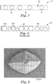
- Figure 8 provides a cross-sectional schematic of an exemplary prior art electrically conductive article 80, including a plurality of sieved electrically conductive spherical particles 84 distributed in a resin 86.
- an electrically conductive article 80 having a thickness of 50 ⁇ m, for example, containing sieved substantially spherical electrically conductive particles 84 would typically contain particles ranging in nominal size from about 20 ⁇ m to about 50 ⁇ m.
- the particles 84a having a diameter close to 50 ⁇ m can participate in z-axis conductivity of the article 80, but the particles 84b having a smaller diameter (e.g., a diameter closer to 20 ⁇ m) are generally too far from at least one of the major surfaces of the resin to participate in z-axis conductivity.
- embodiments according to the present disclosure advantageously require a smaller loading of electrically conductive particles to achieve the same conductivity as when employing a wider size distribution of electrically conductive particles.
- the amount of electrically conductive shaped particles in the electrically conductive article of the present disclosure is optionally expressed in terms of its percent by weight of the composite or in terms of its percent by volume of the composite.
- the use of shaped particles having a narrow size distribution allows the addition of lower loadings of the shaped particles as compared to particles having a wider size distribution, to achieve the same electrical conductivity.
- the composite comprises between 1 wt. % and 95 wt. % of the electrically conductive shaped particles.
- the composite comprises up to 95 wt. % of the electrically conductive shaped particles, or up to 75 wt. %, or up to 50 wt. %, or up to 30 wt.
- the composite comprises at least 1 wt. % of the electrically conductive shaped particles, or at least 5 wt. %, or at least 10 wt. %, or at least 15 wt. %, or at least 20 wt. %, or at least 25 wt. % of the electrically conductive shaped particles. In certain embodiments, the composite comprises between 0.1 volume percent (vol. %) and 25 vol. % of the electrically conductive shaped particles. In certain embodiments, the composite comprises up to 25 vol. % of the electrically conductive shaped particles, or up to 20 vol. %, or up to 15 vol.
- the composite comprises at least 0.1 vol. % of the electrically conductive shaped particles, or at least 0.5 vol. %, or at least 1 vol. %, or at least 5 vol. %, or at least 10 vol. % of the electrically conductive shaped particles
- Providing the electrically conductive shaped particles typically comprises molding a core of each of the electrically conductive shaped particles.
- Several suitable molding methods are described in detail in each of U.S. Patent Nos. 8,034,137 (Erickson et al. ), 8,142,531 (Adefris et al. ), and 8,142,891 (Culler et al. ), and U.S. Application Publication Nos. 2012/0227333 (Adefris et al. ), and 2010/0146867 (Boden et al. ).
- the ability to employ a plurality of particles manufactured to have a monosized dispersion and shape corresponding to the shape of a mold cavity provides an efficient way to provide electrical conductivity to a composite, such as for an electrically conductive article.
- the electrically conductive shaped particles employed have sufficient mechanical strength to be utilized in applications requiring structural integrity.
- the electrically conductive shaped particles comprise a core comprising a Young's modulus of from 0.01 GigaPascal (GPa) to 1,000 GPa, more preferably from 1 GPa to 100 GPa, and most preferably from 10 GPa to 400 GPa.
- each of the electrically conductive shaped particles comprises a core comprising alumina, zirconia, yttria, yttria-stabilized zirconia, silica, titanium carbide, boron carbide, boron nitride, or silicon carbide, and often the core comprises alumina.
- Figure 9 provides a scanning electron microscope (SEM) image of a shaped particle formed of alumina having the shape of a truncated pyramid with four side facets, a base, and a top surface (provided by the truncation of the pyramid).
- Figure 10 provides a SEM image of a five-sided triangle shaped particle formed of alumina.
- Providing the electrically conductive shaped particles usually further comprises applying a metal coating to the core of each of the electrically conductive shaped particles to form the electrically conductive shaped particles.
- the method of coating the cores is not particularly limited, for example and without limitation the metal coating optionally comprises sputtering the metal onto the core of each of the electrically conductive shaped particles.
- Each of the metal coated electrically conductive shaped particles generally comprises a metal coating having an average thickness between 1 micrometer ( ⁇ m) and 50 ⁇ m, or between 1 micrometer ( ⁇ m) and 20 ⁇ m, or between 1 micrometer ( ⁇ m) and 10 ⁇ m.
- the metal coating comprises aluminum, silver, copper, nickel, gold, or alloys thereof, and often silver or copper.
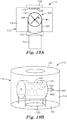
- Figure 11A provides a cross-sectional schematic of an exemplary electrically conductive shaped particle 40 comprising a triangle shape, having a core 42 and a metal coating 44.
- Figure 11B provides a cross-sectional schematic of an exemplary electrically conductive shaped particle 40 comprising a rectangle shape, having a core 42 and a metal coating 44.
- each of the electrically conductive shaped particles comprising a metal coating comprises between 10 percent by weight (wt. %) metal and 40 wt. % metal. In certain embodiments, each of the electrically conductive shaped particles comprises a metal coating comprising up to 70 wt. %, or up to 40 wt. % metal, or up to 25 wt. % metal, or up to 20 wt. % metal, or up to 15 wt. % metal. In certain embodiments, each of the electrically conductive shaped particles comprises a metal coating comprising at least 1 wt. % metal, or at least 10 wt. % metal, or at least 15 wt. % metal, or at least 25 wt.
- each of the electrically conductive shaped particles comprises a metal coating comprising at least 15 wt. % metal. It was discovered that a metal coating level of 15 wt. % or greater typically ensured that sufficient metal was coated on the surface of each of the particles to adequately cover each of the facet surfaces and the edges of the formed surfaces, achieving reliable conductivity from one surface facet to another adjacent facet across an edge.
- each of the electrically conductive shaped particles comprises a metal.
- each of the electrically conductive shaped particles optionally comprises a core comprising aluminum, silver, copper, gold, or alloys thereof.
- the majority of the electrically conductive shaped particles are oriented in the resin of the composite in substantially the same direction.
- the intersection of the first surface and the second surface of at least 30% of the electrically conductive shaped particles is oriented in the resin normal to a major surface of the composite, or at least 70%, or at least 80%, or at least 90%, or at least 95%, or at least 98% of the electrically conductive shaped particles is oriented in the resin normal to a major surface of the composite.
- the resin of the electrically conductive article is not particularly limited, and will typically depend on the specific application for which the article is intended.
- the resin comprises a thermoset polymer, a thermoplastic polymer, or an elastomeric polymer.
- the resin comprises a pressure-sensitive adhesive, a liquid adhesive, a hot melt adhesive, and/or a structural adhesive (e.g., either a 1- or 2-part adhesive).
- the resin optionally comprises an epoxy, a polyurea, an acrylic, a cyanoacrylate, a polyamide, a phenolic, a polyimide, a silicone, a polyester, an aminoplast, a melamine, an acrylated epoxy, a urethane, polyvinyl chloride, or a combination thereof.
- the resin may include a thermosetting material or a thermoplastic material.
- material refers to monomers, oligomers, prepolymers, and/or polymers.
- the resin may include optional additives, and in the case of a resin material including a thermosetting material, may also include a curative or curatives.
- curative is used broadly to include not only those materials that are conventionally regarded as curatives but also those materials that catalyze or accelerate the reaction of the curable material as well as those materials that may act as both curative and catalyst or accelerator.
- thermoplastic refers to a material which undergoes a physical change upon the application of heat, i.e., the material flows upon heating and returns to its initial non-flowing state upon cooling.
- a thermoplastic material is typically bonded by application of heat and/or pressure.
- Thermoplastic adhesives can include hot-melt adhesives.
- Hot melt adhesive can include natural or synthetic rubbers, butyl rubber, nitrile rubbers, synthetic polyisoprene, ethylene-propylene rubber, ethylene-propylene-diene monomer rubber (EPDM), polybutadiene, polyisobutylene, poly(alpha-olefin), styrene-butadiene random copolymer, fluoroelastomers, silicone elastomers, and combinations thereof.
- An alternative to rubber includes polyvinyl chloride (PVC) resins, which are formed by polymerization of the monomer vinyl chloride (VCM).
- thermosetting refers to a material, which undergoes a curing reaction that results in a chemical change upon bonding and an increase in the hardness of the material.
- thermoset refers to a thermosetting material which has been cured.
- a thermosetting material may generally be bonded by application of heat, actinic radiation such as UV, visible, or infrared, or microwave or X-ray energy.
- a thermosetting material may also be caused to cure by mixing two reactive components, for example, by mixing a monomer mixture or oligomer mixture with a curative mixture.
- the resin of the present disclosure can include a heat bondable material which, upon application of heat, undergoes an initial decrease in viscosity which promotes wetting of a substrate in which the article is in contact, and enhances adhesion and, in the case of, for example, a thermosetting material, causes a curing reaction.
- Typical thermosetting adhesives can be epoxy-based adhesives such as, for example, ethylene-glycidyl (meth)acrylate copolymers, phenolic-based adhesives, or (meth)acrylic adhesives. These adhesives can be crosslinked thermally, reactively (including moisture-cured), or photochemically.
- the resin often includes acrylic pressure-sensitive adhesives. Typically, the acrylic pressure-sensitive adhesives are substantially solventless and are UV or visible-light curable.
- Suitable acrylic adhesives include free radically-curing acrylics and cyanoacrylates.
- the term "(meth)acrylic” as used herein refers to acrylic and methacrylic.
- the acrylic adhesives can include conventional additives such as plasticizers, tougheners, flow modifiers, neutralizing agents, stabilizers, antioxidants, fillers, colorants, and the like.
- Suitable free radically-curing acrylics can include, but are not limited to, those formed from methyl methacrylate, methacrylic acid, tetrahydrofurfuryl methacrylate, isobornyl acrylate, and isobornyl methacrylate.
- Multifunctional (meth)acrylic acid esters can optionally be included as crosslinking agents.
- multifunctional (meth)acrylates can include, but are not limited to, ethylene glycol dimethacrylate, 1,6-hexanediol dimethacrylate, 1,6-hexanediol diacrylate, trimethylolpropane triacrylate, pentaerythritol tetraacrylate, 1,2-ethylene glycol diacrylate, the dimethacrylate of ethylene oxide modified bisphenol A and the diacrylate of ethylene oxide modified bisphenol A.
- the (meth)acrylic adhesives can be cured through free radical initiated polymerization.
- the free radicals are generated by a redox reaction.
- Redox initiators can include peroxides, hydroperoxides, metal ions, saccharin, and N,N-dimethyl-p-toluidine.
- the free radicals can be generated in a two-part adhesive system that cures at room temperature after mixing or in a one-part adhesive system.
- the polymerization of the (meth)acrylic adhesive monomers to form a polymer useful in the present disclosure can be carried out using thermal energy, electron-beam radiation, ultraviolet radiation, and the like.
- Such polymerizations can be facilitated by a polymerization initiator, which can be a thermal initiator or a photoinitiator.
- a polymerization initiator which can be a thermal initiator or a photoinitiator.
- suitable photoinitiators include, but are not limited to, benzoin ethers such as benzoin methyl ether and benzoin isopropyl ether, substituted benzoin ethers such as anisoin methyl ether, substituted acetophenones such as 2,2-dimethoxy-2-phenylacetophenone, and substituted alpha-ketols such as 2-methyl-2-hydroxypropiophenone.
- Cyanoacrylate adhesives can include those formed from methyl cyanoacrylate and ethyl cyanoacrylate as well as other cyanoacrylate esters. They can optionally include additives such as hydroquinone.
- the cyanoacrylate adhesive is chosen from adhesives sold by multiple companies under the name of Super Glue Gel, which have enhanced viscosity and appropriately long bondlines.
- Suitable epoxy resins include those formed from monomers having at least two 1,2-cyclic ethers. Such compounds can be saturated or unsaturated, aliphatic, aromatic or heterocyclic, or can include combinations thereof. Suitable epoxides may be solid or liquid at room temperature. It is also within the scope of this disclosure to use a material with functionality in addition to epoxide functionality but which is essentially unreactive with the epoxide functionality, for example, a material containing both epoxide and acrylic functionality. An optional additive is a core-shell toughener. Examples of suitable epoxide-based adhesives that are commercially available include those available from 3M Company, St. Paul, MN under the trade designation "3M SCOTCH-WELD EPOXY ADHESIVE.”
- Suitable epoxy resin compositions may be made from thermally curable epoxy resins.
- the term epoxy resin composition will typically be used to refer to an uncured composition.
- An exemplary epoxy resin composition includes one or more aromatic polyepoxides and one or more 9,9-bis(aminophenyl)fluorene curing agents.
- Suitable aromatic polyepoxides include poly(glycidyl ether)s of polyhydric phenols and epoxy resins available from Shell Chemical Company, Houston, Tex., under the trade designations EPON 1001F and EPON 1050.
- Suitable resins include blends of a diglycidylether of bisphenol A and a novolac epoxy, for example, 75 to 90% by weight EPON 1001F and 25 to 10% by weight EPON 1050F based on the total weight of the resin.
- Suitable curing agents for the epoxy resin compositions include, but are not limited to, di(4-aminophenyl)sulfone and 9,9-bis(aminophenyl)fluorene as described in U.S. Pat. No. 4,684,678 .
- active-hydrogen containing groups include primary alcohols, secondary alcohols, phenols and water.
- Other active-hydrogen containing groups include primary and secondary amines which react with the isocyanate to form a urea linkage, thereby making a polyurea.
- Urethane adhesives can include two-part room temperature-curing adhesives. Urethane adhesives can also include one-part moisture curing adhesives that are applied when warm including those available from 3M company, St. Paul, MN under the trade designation "3M SCOTCH-WELD POLYURETHANE REACTIVE ADHESIVES".
- Suitable phenolic resins are generally described in " Encyclopedia of Polymer Science and Engineering”, Volume 11, John Wiley & Sons, Inc. (New York, 1988), pp. 45-92 . Phenolic-based resins are generally described in Alphonsus V. Pocius, "Adhesion and Adhesives Technology: An Introduction”, Hanser Publishers (New York, 1997), pp.185-188 . Suitable phenolic materials are those made as the reaction product of phenols and formaldehydes, including resole phenolics and novolac phenolics. Examples of phenols include phenol, resorcinol, para-substituted phenol, cresol, and the reaction product of bisphenol-A and the monoglycidyl ether of bisphenol-A.
- Suitable silicone resins include moisture-cured silicones, condensation-cured silicones, and addition-cured silicones, such as hydroxyl-terminated silicones, silicone rubber, and fluorosilicone.
- suitable commercially available silicone pressure-sensitive adhesive compositions comprising silicone resin include Dow Coming's 280A, 282, 7355, 7358, 7502, 7657, Q2-7406, Q2-7566 and Q2-7735; General Electric's PSA 590, PSA 600, PSA 595, PSA 610, PSA 518 (medium phenyl content), PSA 6574 (high phenyl content), and PSA 529, PSA 750-D1, PSA 825-D1, and PSA 800-C.
- An example of a two-part silicone resin is commercially available under the trade designation " SILASTIC J" from Dow Chemical Company, Midland, MI .
- Suitable polyurea resins include those prepared by reacting an isocyanate-functional material with an amine-functional material.
- the polyurea is included in a pressure-sensitive adhesive or a thermosetting adhesive.
- a polyurea-based polymer comprises a segmented copolymer, in which at least about 0.5 mole fraction of linkages between segments in a backbone of the polymer are urea linkages.
- Polyester resins include polymers having monomer units linked together by an ester group, i.e., -COO-. Typically, polyester resins are formed by polymerizing a polyhydric alcohol with a polybasic acid. Exemplary polyester resins include polyethylene terephthalate (PET) and polyethylene terephtalate glycol (PETG).
- PET polyethylene terephthalate
- PETG polyethylene terephtalate glycol
- Suitable polyimide resins include those prepared by reacting primary aliphatic diamines and dicarboxylic dianhydrides, such as reacting pyromellitic dianhydride with 4,4'-oxydianiline. Curing is typically accomplished by eliminating water via heating to close the imide rings present along the polymer chain, thereby forming the polyimide structure.
- Polyamide resin materials are characterized by having an amide group, i.e., -C(O)NH-.
- the polyamide resin materials usually include polyamide hot melt adhesives. Suitable polyamides include for example terpolymers produced from lactams (such as lauryl lactam) and diamines. Commercially available thermoplastic polyamides include those having the trade designations VESTAMELT 732, VESTAMELT 730, VESTAMELT 742, VESTAMELT 750/751, VESTAMELT 755, and VESTAMELT 760, from Creanova, Somerset, N.J.
- Melamine resins are amino resins formed from a condensation polymerization of trimethylol melamine, typically also reacting with melamine and formaldehyde. Further, butylated melamine resins are optionally formed by including alcohols such as butyl during the polymerization.
- Aminoplast resins are thermosetting adhesives formed by condensation of an amine-containing compound with an aldehyde. Suitable amine-containing compounds include for example melamine or urea. Some useful aminoplast resins can be monomeric or oligomeric. Typically, the aminoplast resins have at least one pendant ⁇ , ⁇ -unsaturated carbonyl group per molecule. These ⁇ , ⁇ -unsaturated carbonyl groups can be acrylate, methacrylate, or acrylamide groups. Examples of such resins include N-hydroxymethyl-acrylamide, N,N'-oxydimethylenebisacrylamide, ortho and para acrylamidomethylated phenol, acrylamidomethylated phenolic novolac, and combinations thereof. These materials are further described in U.S. Pat. Nos. 4,903,440 and 5,236,472 , which are incorporated herein by reference.
- the resin may comprise at least one of a grease or wax.
- Suitable commercially available greases include non-silicone resin systems having the trade designations 3M THERMALLY CONDUCTIVE GREASE TCG-2035 AND 3M THERMALLY CONDUCTIVE GREASE TCG-2031, from 3M Company, St. Paul, MN.
- Waxes include long alkyl chains, either with or without functional groups such as fatty acid esters and alcohols. Waxes or mixtures of waxes which may be used include materials of vegetable, animal, petroleum, and/or mineral derived origin.
- Representative waxes include carnauba wax, candelilla wax, oxidized Fischer-Tropsch wax, microcrystalline wax, lanolin; bayberry wax, palm kernal wax, mutton tallow wax, emulsifiable polyethylene wax, polyethylene copolymer wax, emulsifiable petroleum derived waxes, montan wax derivatives, emulsifiable polypropylene wax, and oxidized polyethylene wax.
- the composite further comprises a plurality of conductive fillers comprising an aspect ratio of length to height of greater than 2:1, or greater than 4:1, or greater than 10:1.
- the length is the longest dimension and the height is the smallest dimension (with the width equal to or greater than the height).
- Such conductive fillers typically provide conductivity in the x-y plane, which adds to the electrical conductivity in the z-axis being provided by the electrically conductive shaped particles in the composite.
- Figure 12 is a cross-sectional schematic of an exemplary electrically conductive article 10, including a composite 12 comprising a plurality of electrically conductive shaped particles 14 comprising a trapezoid shape and a plurality of conductive fillers 17 distributed in a resin 16.
- Figure 13 is a cross-sectional schematic of an exemplary electrically conductive article 10, including a composite 12 comprising a plurality of electrically conductive shaped particles 14 comprising a rhombus shape and a plurality of conductive fillers 17 distributed in a resin 16.
- the plurality of conductive fillers is not particularly limited, and optionally comprises fibers, shards, woven and/or nonwoven scrims, coated with metal.
- the fibers, shards, woven and nonwoven scrims comprise glass, polymer, carbon, or ceramic.
- Figure 14 provides a cross-sectional schematic of an exemplary conductive coated fiber 60 comprising a needle shape, having a fiber 62 and a metal coating 64.
- the plurality of conductive fillers comprises carbon black or graphene based materials, for example doped or undoped graphene.
- Suitable graphene based materials comprise for example and without limitation, flakes, exfoliated graphite, graphene nanoplatelets, functionalized graphene sheets, or a combination thereof.
- the electrically conductive article further comprises conductive and/or non-conductive fillers having a typical particle size distribution (i.e., not monosized), to enhance the performance of the article.
- conductive and/or non-conductive fillers having a typical particle size distribution (i.e., not monosized), to enhance the performance of the article.
- Such fillers are used primarily to enhance EMI shielding EMI absorbing, and/or thermal conductivity of the composite, or to modify composite properties for shear strength, flow characteristics, fracture resistance, and/or environmental stability.
- the electrically conductive article comprises a substrate, wherein the composite is attached to a major surface of the substrate.
- the substrate is not particularly limited, and often comprises a nonwoven material, a woven material, a metal foil, a polymer, or a (woven) fabric. Such substrates are often employed when the electrically conductive article comprises an adhesive tape.
- the electrically conductive article comprises a substrate provided between two layers of electrically conductive resin, thus providing a double-sided electrically conductive article.
- Figure 15 provides a cross-sectional schematic of an exemplary electrically conductive article 10, including a composite 12 comprising a plurality of electrically conductive shaped particles 14 comprising a diamond shape distributed in a resin 16, and an electrically conductive internal substrate 92 positioned approximately in the center of the thickness of the article 10.
- the height of the plurality of electrically conductive shaped particles 14 allows the particles to contact both the internal substrate 92 and one major surface 94, for instance, of the composite 12, thus two rows of electrically conductive shaped particles 14 are included to cooperatively provide conductivity through the thickness of the article 10 when it is in use (e.g., subjected to compression between two materials).
- Figure 16 provides a cross-sectional schematic of an exemplary electrically conductive article 10, including a composite 12 comprising a first plurality of electrically conductive shaped particles 14a and a second plurality of electrically conductive shaped particles 14b, each comprising a diamond shape, distributed in a resin 16.
- the article further includes an electrically conductive internal substrate 92 positioned approximately in the center of the thickness of the article 10.
- the height of the first plurality of electrically conductive shaped particles 14a allows the particles to contact both the internal substrate 92 and one major surface 94 of the composite 12, whereas the height of the second plurality of electrically conductive shaped particles 14b (approximately twice that of the first shaped particles 14a) allows the second shaped particles 14b to contact both major surfaces of the composite 12, and penetrate through the internal substrate 92, to provide conductivity through the thickness of the article 10 when it is in use (e.g., subjected to compression between two materials).
- Figure 17 provides a cross-sectional schematic of an exemplary electrically conductive article 10, including a composite 12 comprising a first plurality of electrically conductive shaped particles 14a comprising a trapezoid shape and a second plurality of electrically conductive shaped particles 14b comprising a diamond shape, distributed in a resin 16.
- the article further includes an electrically conductive internal substrate 92 positioned at approximately one third of the distance of the thickness of the article 10.
- the height of the first plurality of electrically conductive shaped particles 14a allows the particles to contact both the internal substrate 92 and a first major surface 94 of the composite 12, whereas the height of the second plurality of electrically conductive shaped particles 14b allows the particles to contact both the internal substrate and a second, opposing, major surface 96 of the composite 12.
- one row of the first shaped particles 14a and one row of the second shaped particles 14b are included to cooperatively provide conductivity through the thickness of the article 10 when it is in use (e.g., subjected to compression between two materials).
- Figure 18 provides a cross-sectional schematic of an exemplary electrically conductive article 10, including a composite 12 comprising a first plurality of electrically conductive shaped particles 14a comprising a trapezoid shape and a second plurality of electrically conductive shaped particles 14b comprising a diamond shape, distributed in a resin 16.
- the article further includes an electrically conductive internal substrate 92 positioned approximately in the center of the thickness of the article 10.
- the height of the first plurality of electrically conductive shaped particles 14a allows the particles to contact both the internal substrate and a first major surface 94 of the composite 12, whereas the height of the second plurality of electrically conductive shaped particles 14b allows the particles to contact both the internal substrate 92 and a second, opposing, major surface 96 of the composite 12.
- the electrically conductive shaped particles partially penetrate the internal electrically conductive substrate 92 due to its loose, nonwoven (or in some cases woven) structure.
- one row of the first shaped particles 14a and one row of the second shaped particles 14b are included to cooperatively provide conductivity through the thickness of the article 10 when it is in use (e.g., subjected to compression between two materials).
- the electrically conductive article exhibits a contact resistance of the z-axis of less than 100.00 ohms, or less than 10.00 ohms, or less than 2.00 ohms, or less than 0.05 ohms, such as between 0.005 and 1.00 ohms, or between 0.05 and 1.00 ohms, or between 0.05 and 0.80 ohms, or between 0.05 and 0.60 ohms, or between 0.05 and 0.40 ohms, or between 0.005 and 0.40 ohms, as measured by standard contact resistance tests.
- boehmite sol-gel was made using the following recipe: aluminum oxide monohydrate powder (1600 parts) having the trade designation "DISPERAL” (commercially available from Sasol North America, Inc.) was dispersed by high shear mixing a solution containing water (2400 parts) and 70 percent aqueous nitric acid (72 parts) for 5 minutes. The resulting sol-gel was aged for at least 1 hour before coating. A mold release agent, 1 percent peanut oil in methanol was used to coat the production tooling with about 0.5 milligram per square inch (mg/in 2 ) (3.2 milligram per square centimeter (mg/cm 2 )) of peanut oil applied to the production tooling.
- DISPERAL trade designation
- a mold release agent 1 percent peanut oil in methanol was used to coat the production tooling with about 0.5 milligram per square inch (mg/in 2 ) (3.2 milligram per square centimeter (mg/cm 2 )) of peanut oil applied to the production tooling.
- the sol-gel was forced into production tooling having triangular shaped mold cavities of 8 mils (203.2 micrometers ( ⁇ m)) depth and 27 mils (685.8 ⁇ m) on each side.
- the draft angle ⁇ between the sidewall and bottom of the mold was 98 degrees.
- the sol-gel was forced into the cavities with a putty knife so that the openings of the production tooling were completely filled.
- Excess methanol was removed by placing sheets of the production tooling in an air convection oven for 5 minutes at 45 degrees Celsius.
- the sol-gel coated production tooling was placed in an air convection oven at 45 degrees Celsius for at least 45 minutes to dry.
- the precursor shaped abrasive particles were removed from the production tooling by passing it over an ultrasonic horn.
- the precursor shaped abrasive particles were calcined at approximately 650 degrees Celsius and then saturated with a mixed nitrate solution of the following concentration (reported as oxides): 1.8 percent each of MgO, Y 2 O 3 , Nd 2 O 3 and La 2 O 3 .
- the excess nitrate solution was removed and the saturated precursor shaped abrasive particles with openings were allowed to dry after which the particles were again calcined at 650 degrees Celsius and sintered at approximately 1400 degrees Celsius. Both the calcining and sintering was performed using rotary tube kilns.
- 5-sided truncated pyramid shaped particles were produced using the same procedure described above except the production tooling was changed to a production tooling having right rhombic pyramidal shaped mold cavities of dimensions as shown in Table 1.
- the surfaces of the mold cavities were manufactured to have a series grooves with triangular cross sections. The grooves were 6 micrometers deep and had a 110 degree tip angle dimension. Table 1.
- IPC Multi-Purpose test board (IPC-B-25A) (Diversified Systems, Inc, Indianapolis, Ind.) was used to measure the conductivity of the composite in the Z-axis direction.
- IPC-B-25A IPC Multi-Purpose test board
- the composite sample was laminated over a portion of a 2.7 millimeter (mm) wide, gold plated copper trace on a polyimide film. A portion of the gold plated copper trace was not covered by the composite.
- the polyimide test strip was laminated over the 2.1 mm wide traces on the IPC-B-25 test board.
- Heat and pressure bonding, compression, or combinations thereof were available for non-adhesive composites.
- the portion of the gold plated copper trace that was not covered with the composite was clamped into contact with one of the other traces on the IPC test board.
- the resistance was measured by probing the IPC trace that was in contact with the composite and the IPC trace that was in contact with the gold plated trace on the polyimide film.
- Samples were dwelled for 1 hour and for 24 hours at room temperature conditions (20-23°C at 20-50% relative humidity) after the test configuration was set, prior to resistance testing.
- the polyimide film and composite were applied to a Stainless Steel (SS) substrate with a section of the polyimide film away from the SS substrate.
- the overlap of the film/composite onto the SS substrate was 10 mm.
- the contact resistance was measured between the film and the SS substrate with resistance probes. Samples were dwelled for 1 hour and for 24 hours at room temperature conditions (20-23°C at 20-50% relative humidity) after the test configuration was set, prior to resistance testing.
- the apparatus 110 includes a housing 112 defining a vacuum chamber 114 containing a particle agitator 116.
- the housing 112 which may be made from an aluminum alloy if desired, is a vertically oriented hollow cylinder (45 centimeters (cm) high and 50 cm in diameter).
- the base 118 contains a port 120 for a high vacuum gate valve 122 followed by a six-inch diffusion pump 124 as well as a support 126 for the particle agitator 116.
- the chamber 114 is capable of being evacuated to background pressures in the range of 10 -6 torr.
- the top of the housing 112 includes a demountable, rubber L-gasket sealed plate 128 that is fitted with an external mount three-inch diameter dc magnetron sputter deposition source 130 (a US Gun II, US, INC., San Jose, CA).
- a metal sputter target 132 (5 inches x 8 inches and 0.5 inches thick) (12.7 cm x 20.32 cm and 1.27 cm thick).
- the sputter source 130 is powered by an MDX-10 Magnetron Drive (Advanced Energy Industries, Inc, Fort Collins, CO) fitted with an arc suppressing Sparc-le 20 (Advanced Energy Industries, Inc, Fort Collins, CO).
- the particle agitator 116 is a hollow cylinder (2.00 inches long x 2.25 inches diameter horizontal) (5.08 cm long x 5.715 cm diameter horizontal) with a rectangular opening 34 (1.25 inches x 1.75 inches) (3.175 inches x 4.445 inches) in the top 136.
- the opening 134 is positioned 7 centimeters directly below the surface 136 of the sputter target 132 so that sputtered metal atoms can enter the agitator volume 138.
- the agitator 116 is fitted with a shaft 140 aligned with its axis.
- the shaft 140 has a rectangular cross section to which are bolted four rectangular blades 142 which form an agitation mechanism or paddle wheel for the support particles being tumbled.
- the blades 142 each contain two holes 144 to promote communication between the particle volumes contained in each of the four quadrants formed by the blades 142 and agitator cylinder 116.
- alumina shaped particles Forty cubic centimeters (cc) (125g) of alumina shaped particles were used as the substrate.
- the particles were placed into the particle agitator apparatus 110, and the chamber 114 was then evacuated. Once the chamber pressure was in the 10 -5 torr range, the argon sputtering gas was admitted to the chamber 114 at a pressure of about 110 millitorr. Pure Ag metal was used as the sputter target 132.
- the deposition process was then started by applying a cathodic power of 2.00 kilowatts.
- the particle agitator shaft 140 was rotated at about 4 rpm during the Ag deposition process. The power was stopped after 6 hours.
- the chamber 114 was backfilled with air and the Ag coated particles were removed from the apparatus 110.
- Example 1 Electrically Conductive Adhesive Transfer Tape with 5-Sided Pyramid Alumina Shaved Particles:
- Example 1 shaped particles (see Figure 10 ) were obtained and made conductive by coating silver metal on the particles according to the Sputtering Method above.
- a mixture of Acrylate syrup Ag coated shaped alumina particles was prepared according to the sample formulation in Table 3 below. The mixture was put in a small glass container and a tongue depressor was used to mix the shaped particles in the syrup by hand. Finally, the mixture was poured out into a 6 inch (15.24 cm) width silicone coated polyester terephthalate (PET) release liner ⁇ T50 (125 ⁇ m thick) and T10 (50 ⁇ m thick) ⁇ , with the two release sides facing each other and coated using a notch bar coater.
- PET silicone coated polyester terephthalate
- the coating was complete it was cured with UV radiation from the top side for 10 minutes, using a Sylvania bulb at a power of 2.0 - 2.2 mW/cm 2 , for a time of 10 minutes.
- test coupons were cut out and tested using the Stainless Steel Resistance Test above and the Z-Axis Resistance Test above.
- Table 3 lists the electrical data from Example 1.
- the contact resistance (R) data from the standard SS (stainless steel test) and the Z axis test show that all of the values of R are less than 1 ⁇ .
- Example 2 Electrically Conductive Adhesive Transfer Tape with 5-Sided Triangle Alumina Shaved Particles:
- Example 2 shaped particles (see Figure 9 ) were obtained and made conductive by coating silver metal on the particles according to the Sputtering Method above.
- a mixture of Acrylate syrup Ag coated shaped alumina particles was prepared according to the sample formulation in Table 3 below. The mixture was put in a small glass container and a tongue depressor was used to mix the shaped particles in the syrup by hand. Finally, the mixture was poured out into a 6 inch (15.24 cm) width silicone coated polyester terephthalate (PET) release liner ⁇ T50 (125 ⁇ m thick) and T10 (50 ⁇ m thick) ⁇ , with the two release sides facing each other and coated using a notch bar coater.
- PET silicone coated polyester terephthalate
- the coating was complete it was cured with UV radiation from the top side for 10 minutes, using a Sylvania bulb at a power of 2.0 - 2.2 mW/cm 2 , for a time of 10 minutes.
- test coupons were cut out and tested using the Stainless Steel Resistance Test above and the Z-Axis Resistance Test above.
- Table 3 below lists the electrical data from Example 2.
- the contact resistance (R) data from the standard SS (stainless steel test) and the Z axis test show that all of the values of R are less than 1 ohm ( ⁇ ), except for the Stainless Steel Test with a 24 hour dwell time.
- Table 3. Ex. # Sample Formulation Stainless Steel Test (1 hour dwell) Stainless Steel Test (24 hour dwell) Z-Axis Test (1 hour dwell) Z-Axis Test (24 hour dwell) ( ⁇ ) ( ⁇ ) ( ⁇ ) 1 21.2 wt. % Ag coated truncated pyramid shaped particles + 78.8 wt. % Acrylate Syrup 0.77 1.13 0.36 0.59 2 21.2 wt. % Ag coated triangle shaped particles + 78.8 wt. % Acrylate Syrup 0.35 0.69 0.34 0.68
Landscapes
- Physics & Mathematics (AREA)
- Chemical & Material Sciences (AREA)
- Dispersion Chemistry (AREA)
- Spectroscopy & Molecular Physics (AREA)
- Engineering & Computer Science (AREA)
- Microelectronics & Electronic Packaging (AREA)
- Compositions Of Macromolecular Compounds (AREA)
- Conductive Materials (AREA)
- Non-Insulated Conductors (AREA)
- Manufacturing Of Electric Cables (AREA)
Applications Claiming Priority (2)
| Application Number | Priority Date | Filing Date | Title |
|---|---|---|---|
| US201361904656P | 2013-11-15 | 2013-11-15 | |
| PCT/US2014/064728 WO2015073346A1 (en) | 2013-11-15 | 2014-11-10 | An electrically conductive article containing shaped particles and methods of making same |
Publications (2)
| Publication Number | Publication Date |
|---|---|
| EP3069353A1 EP3069353A1 (en) | 2016-09-21 |
| EP3069353B1 true EP3069353B1 (en) | 2019-10-30 |
Family
ID=51987485
Family Applications (1)
| Application Number | Title | Priority Date | Filing Date |
|---|---|---|---|
| EP14803303.8A Active EP3069353B1 (en) | 2013-11-15 | 2014-11-10 | An electrically conductive article containing shaped particles and methods of making same |
Country Status (5)
| Country | Link |
|---|---|
| US (1) | US10785900B2 (zh) |
| EP (1) | EP3069353B1 (zh) |
| JP (1) | JP6591413B2 (zh) |
| CN (1) | CN105706181B (zh) |
| WO (1) | WO2015073346A1 (zh) |
Families Citing this family (40)
| Publication number | Priority date | Publication date | Assignee | Title |
|---|---|---|---|---|
| CN103764349B (zh) | 2011-06-30 | 2017-06-09 | 圣戈本陶瓷及塑料股份有限公司 | 液相烧结碳化硅研磨颗粒 |
| US8986409B2 (en) | 2011-06-30 | 2015-03-24 | Saint-Gobain Ceramics & Plastics, Inc. | Abrasive articles including abrasive particles of silicon nitride |
| WO2013049239A1 (en) | 2011-09-26 | 2013-04-04 | Saint-Gobain Ceramics & Plastics, Inc. | Abrasive articles including abrasive particulate materials, coated abrasives using the abrasive particulate materials and methods of forming |
| EP2797716B1 (en) | 2011-12-30 | 2021-02-17 | Saint-Gobain Ceramics & Plastics, Inc. | Composite shaped abrasive particles and method of forming same |
| KR102074138B1 (ko) | 2011-12-30 | 2020-02-07 | 생-고뱅 세라믹스 앤드 플라스틱스, 인코포레이티드 | 형상화 연마입자 및 이의 형성방법 |
| US8840696B2 (en) | 2012-01-10 | 2014-09-23 | Saint-Gobain Ceramics & Plastics, Inc. | Abrasive particles having particular shapes and methods of forming such particles |
| BR112014017050B1 (pt) | 2012-01-10 | 2021-05-11 | Saint-Gobain Ceramics & Plastics, Inc. | partícula abrasiva moldada |
| US9242346B2 (en) | 2012-03-30 | 2016-01-26 | Saint-Gobain Abrasives, Inc. | Abrasive products having fibrillated fibers |
| US9200187B2 (en) | 2012-05-23 | 2015-12-01 | Saint-Gobain Ceramics & Plastics, Inc. | Shaped abrasive particles and methods of forming same |
| IN2015DN00343A (zh) | 2012-06-29 | 2015-06-12 | Saint Gobain Ceramics | |
| RU2614488C2 (ru) | 2012-10-15 | 2017-03-28 | Сен-Гобен Абразивс, Инк. | Абразивные частицы, имеющие определенные формы, и способы формирования таких частиц |
| KR101818946B1 (ko) | 2012-12-31 | 2018-01-17 | 생-고뱅 세라믹스 앤드 플라스틱스, 인코포레이티드 | 미립자 소재 및 이의 형성방법 |
| PL2978566T3 (pl) | 2013-03-29 | 2024-07-15 | Saint-Gobain Abrasives, Inc. | Cząstki ścierne o określonych kształtach i sposoby formowania takich cząstek |
| TW201502263A (zh) | 2013-06-28 | 2015-01-16 | Saint Gobain Ceramics | 包含成形研磨粒子之研磨物品 |
| CA3114978A1 (en) | 2013-09-30 | 2015-04-02 | Saint-Gobain Ceramics & Plastics, Inc. | Shaped abrasive particles and methods of forming same |
| US9566689B2 (en) | 2013-12-31 | 2017-02-14 | Saint-Gobain Abrasives, Inc. | Abrasive article including shaped abrasive particles |
| US9771507B2 (en) | 2014-01-31 | 2017-09-26 | Saint-Gobain Ceramics & Plastics, Inc. | Shaped abrasive particle including dopant material and method of forming same |
| KR101890106B1 (ko) | 2014-04-14 | 2018-08-22 | 생-고뱅 세라믹스 앤드 플라스틱스, 인코포레이티드 | 형상화 연마 입자들을 포함하는 연마 물품 |
| US9803119B2 (en) | 2014-04-14 | 2017-10-31 | Saint-Gobain Ceramics & Plastics, Inc. | Abrasive article including shaped abrasive particles |
| US9902045B2 (en) | 2014-05-30 | 2018-02-27 | Saint-Gobain Abrasives, Inc. | Method of using an abrasive article including shaped abrasive particles |
| US9707529B2 (en) | 2014-12-23 | 2017-07-18 | Saint-Gobain Ceramics & Plastics, Inc. | Composite shaped abrasive particles and method of forming same |
| US9914864B2 (en) | 2014-12-23 | 2018-03-13 | Saint-Gobain Ceramics & Plastics, Inc. | Shaped abrasive particles and method of forming same |
| US9676981B2 (en) | 2014-12-24 | 2017-06-13 | Saint-Gobain Ceramics & Plastics, Inc. | Shaped abrasive particle fractions and method of forming same |
| TWI634200B (zh) | 2015-03-31 | 2018-09-01 | 聖高拜磨料有限公司 | 固定磨料物品及其形成方法 |
| EP3277459B1 (en) | 2015-03-31 | 2023-08-16 | Saint-Gobain Abrasives, Inc. | Fixed abrasive articles and methods of forming same |
| CA3118262C (en) | 2015-06-11 | 2023-09-19 | Saint-Gobain Ceramics & Plastics, Inc. | Abrasive article including shaped abrasive particles |
| MX2018005764A (es) * | 2015-11-12 | 2018-08-01 | Cytec Ind Inc | Velo hibrido como capa intercalar en materiales compuestos. |
| KR102481559B1 (ko) | 2016-05-10 | 2022-12-28 | 생-고뱅 세라믹스 앤드 플라스틱스, 인코포레이티드 | 연마 입자 및 이의 형성 방법 |
| KR102313436B1 (ko) | 2016-05-10 | 2021-10-19 | 생-고뱅 세라믹스 앤드 플라스틱스, 인코포레이티드 | 연마 입자들 및 그 형성 방법 |
| WO2018064642A1 (en) | 2016-09-29 | 2018-04-05 | Saint-Gobain Abrasives, Inc. | Fixed abrasive articles and methods of forming same |
| US10964441B2 (en) | 2016-12-21 | 2021-03-30 | 3M Innovative Properties Company | Conductive particles, articles, and methods |
| US10563105B2 (en) | 2017-01-31 | 2020-02-18 | Saint-Gobain Ceramics & Plastics, Inc. | Abrasive article including shaped abrasive particles |
| US10759024B2 (en) | 2017-01-31 | 2020-09-01 | Saint-Gobain Ceramics & Plastics, Inc. | Abrasive article including shaped abrasive particles |
| WO2018205127A1 (en) | 2017-05-09 | 2018-11-15 | 3M Innovative Properties Company | Electrically conductive adhesive |
| CN110719946B (zh) | 2017-06-21 | 2022-07-15 | 圣戈本陶瓷及塑料股份有限公司 | 颗粒材料及其形成方法 |
| JP7049459B2 (ja) | 2017-12-22 | 2022-04-06 | エッカルト ゲゼルシャフト ミット ベシュレンクテル ハフツング | 導電性粒子、組成物、物品、及び導電性粒子の製造方法 |
| CN109688782A (zh) * | 2019-01-31 | 2019-04-26 | 常州斯威克新材料科技有限公司 | 一种无导电颗粒电磁屏蔽膜及其制备方法 |
| WO2021133901A1 (en) | 2019-12-27 | 2021-07-01 | Saint-Gobain Ceramics & Plastics, Inc. | Abrasive articles and methods of forming same |
| KR102474337B1 (ko) * | 2020-08-28 | 2022-12-07 | 주식회사 아이에스시 | 전기접속용 커넥터 |
| KR102582710B1 (ko) * | 2021-12-29 | 2023-09-26 | 주식회사 아이에스시 | 도전성 입자의 제조방법 및 도전성 입자 |
Family Cites Families (24)
| Publication number | Priority date | Publication date | Assignee | Title |
|---|---|---|---|---|
| US3475213A (en) | 1965-09-13 | 1969-10-28 | Minnesota Mining & Mfg | Electrically conductive adhesive tape |
| US4684678A (en) | 1985-05-30 | 1987-08-04 | Minnesota Mining And Manufacturing Company | Epoxy resin curing agent, process, and composition |
| US4903440A (en) | 1988-11-23 | 1990-02-27 | Minnesota Mining And Manufacturing Company | Abrasive product having binder comprising an aminoplast resin |
| US5236472A (en) | 1991-02-22 | 1993-08-17 | Minnesota Mining And Manufacturing Company | Abrasive product having a binder comprising an aminoplast binder |
| US5443876A (en) | 1993-12-30 | 1995-08-22 | Minnesota Mining And Manufacturing Company | Electrically conductive structured sheets |
| JP2004035686A (ja) | 2002-07-02 | 2004-02-05 | Bridgestone Corp | 異方性導電フィルム |
| US7790063B2 (en) | 2003-09-26 | 2010-09-07 | Hitachi Chemical Company, Ltd. | Mixed conductive power and use thereof |
| GB0427164D0 (en) * | 2004-12-11 | 2005-01-12 | Eastman Kodak Co | Conductive silver dispersions and uses thereof |
| JP4319167B2 (ja) | 2005-05-13 | 2009-08-26 | タツタ システム・エレクトロニクス株式会社 | シールドフィルム、シールドプリント配線板、シールドフレキシブルプリント配線板、シールドフィルムの製造方法及びシールドプリント配線板の製造方法 |
| CN101288133B (zh) * | 2005-09-29 | 2011-01-26 | 阿尔法科学株式会社 | 导电粉及其制造方法、导电粉膏以及导电粉膏的制造方法 |
| JP4924167B2 (ja) | 2006-04-13 | 2012-04-25 | 日立化成工業株式会社 | 導電性ペースト、並びにこれを用いたプリプレグ、金属箔張積層板、及びプリント配線板 |
| CN101495587B (zh) | 2006-07-24 | 2011-08-10 | 3M创新有限公司 | 导电压敏粘合剂 |
| GB0622060D0 (en) * | 2006-11-06 | 2006-12-13 | Hexcel Composites Ltd | Improved composite materials |
| WO2008064215A2 (en) * | 2006-11-20 | 2008-05-29 | Sabic Innovative Plastics Ip Bv | Thermally regulated electrically conducting compositions |
| JP4922793B2 (ja) | 2007-03-09 | 2012-04-25 | アルファーサイエンティフィック株式会社 | 混合導電粉及びその製造方法並びに導電ペースト及びその製造方法 |
| WO2009054386A1 (ja) * | 2007-10-22 | 2009-04-30 | Nippon Chemical Industrial Co., Ltd. | 被覆導電性粉体およびそれを用いた導電性接着剤 |
| JP5414694B2 (ja) | 2007-12-27 | 2014-02-12 | スリーエム イノベイティブ プロパティズ カンパニー | 成形され断裂された研磨粒子及びこの研磨粒子を使用する研磨物品、並びにそれらの作製方法 |
| US8142531B2 (en) | 2008-12-17 | 2012-03-27 | 3M Innovative Properties Company | Shaped abrasive particles with a sloping sidewall |
| US8142891B2 (en) | 2008-12-17 | 2012-03-27 | 3M Innovative Properties Company | Dish-shaped abrasive particles with a recessed surface |
| JP5525546B2 (ja) | 2008-12-17 | 2014-06-18 | スリーエム イノベイティブ プロパティズ カンパニー | 溝を有する成形された研磨粒子 |
| WO2011068714A2 (en) | 2009-12-02 | 2011-06-09 | 3M Innovative Properties Company | Dual tapered shaped abrasive particles |
| JP2011150836A (ja) | 2010-01-20 | 2011-08-04 | Jsr Corp | 回路接続部材、導電性粒子および導電性粒子の製造方法 |
| EP2638990B1 (en) * | 2010-11-08 | 2019-05-08 | Namics Corporation | Manufacturing method for metal particles |
| CN103231072B (zh) * | 2013-04-09 | 2015-06-03 | 昆明理工大学 | 高温电子浆料用二氧化硅/银核壳复合粉的制备方法 |
-
2014
- 2014-11-10 JP JP2016530915A patent/JP6591413B2/ja active Active
- 2014-11-10 CN CN201480061407.3A patent/CN105706181B/zh active Active
- 2014-11-10 US US15/027,496 patent/US10785900B2/en active Active
- 2014-11-10 WO PCT/US2014/064728 patent/WO2015073346A1/en active Application Filing
- 2014-11-10 EP EP14803303.8A patent/EP3069353B1/en active Active
Non-Patent Citations (1)
| Title |
|---|
| None * |
Also Published As
| Publication number | Publication date |
|---|---|
| US20160249495A1 (en) | 2016-08-25 |
| WO2015073346A1 (en) | 2015-05-21 |
| CN105706181B (zh) | 2018-11-16 |
| US10785900B2 (en) | 2020-09-22 |
| CN105706181A (zh) | 2016-06-22 |
| JP2016541098A (ja) | 2016-12-28 |
| JP6591413B2 (ja) | 2019-10-16 |
| EP3069353A1 (en) | 2016-09-21 |
Similar Documents
| Publication | Publication Date | Title |
|---|---|---|
| EP3069353B1 (en) | An electrically conductive article containing shaped particles and methods of making same | |
| EP3605602B1 (en) | Heat-conducting member and heat-dissipating structure including said heat-conducting member | |
| CN1965045B (zh) | 包括空心部分的粘合片及其制备方法 | |
| KR101331679B1 (ko) | 전기 전도성 감압 접착제 | |
| KR101550083B1 (ko) | 방열 시트 및 방열 장치 | |
| KR101523332B1 (ko) | 점착 시트, 전자파 쉴드 시트 및 전자 기기 | |
| JP5423455B2 (ja) | 熱伝導シート、その製造方法及び熱伝導シートを用いた放熱装置 | |
| JP5774472B2 (ja) | 熱強化された電気絶縁性接着ペースト | |
| WO2015072487A1 (ja) | 電磁波吸収放熱シート | |
| JP2006228475A (ja) | 導電性微粒子及び異方性導電材料 | |
| JP2013136766A (ja) | 向上した機能を有する熱伝導性接着テープ | |
| JP2006228474A (ja) | 導電性微粒子及び異方性導電材料 | |
| CN102197069A (zh) | 导热片材、其制造方法以及使用了该导热片材的散热装置 | |
| SE528186C2 (sv) | Slipartikel, slipsegment och segmenterad slipskiva, och förfarande för framställning av dessa | |
| JP4893415B2 (ja) | 放熱性フィルム | |
| US11548264B2 (en) | Insulation sheet, laminate, and substrate | |
| JP2017059704A (ja) | 熱伝導組成物、熱伝導シート、熱伝導シートの製造方法、及び部材 | |
| JP6679839B2 (ja) | 粘着テープ及びその製造方法ならびに放熱フィルム | |
| JPWO2012067194A1 (ja) | 多層樹脂シート及び樹脂シート積層体 | |
| JP2020098905A (ja) | 電子部品搭載基板および電子機器 | |
| KR102425833B1 (ko) | 자기장 차폐시트 및 이를 포함하는 안테나 모듈 | |
| KR20170040776A (ko) | 자성시트 제조방법 | |
| JP6983345B1 (ja) | 熱伝導性シート、および電子機器 | |
| US20230055151A1 (en) | Thermal interface layer | |
| US20230059388A1 (en) | Magnetic film |
Legal Events
| Date | Code | Title | Description |
|---|---|---|---|
| PUAI | Public reference made under article 153(3) epc to a published international application that has entered the european phase |
Free format text: ORIGINAL CODE: 0009012 |
|
| 17P | Request for examination filed |
Effective date: 20160517 |
|
| AK | Designated contracting states |
Kind code of ref document: A1 Designated state(s): AL AT BE BG CH CY CZ DE DK EE ES FI FR GB GR HR HU IE IS IT LI LT LU LV MC MK MT NL NO PL PT RO RS SE SI SK SM TR |
|
| AX | Request for extension of the european patent |
Extension state: BA ME |
|
| DAX | Request for extension of the european patent (deleted) | ||
| STAA | Information on the status of an ep patent application or granted ep patent |
Free format text: STATUS: EXAMINATION IS IN PROGRESS |
|
| 17Q | First examination report despatched |
Effective date: 20181016 |
|
| GRAP | Despatch of communication of intention to grant a patent |
Free format text: ORIGINAL CODE: EPIDOSNIGR1 |
|
| STAA | Information on the status of an ep patent application or granted ep patent |
Free format text: STATUS: GRANT OF PATENT IS INTENDED |
|
| INTG | Intention to grant announced |
Effective date: 20190529 |
|
| GRAS | Grant fee paid |
Free format text: ORIGINAL CODE: EPIDOSNIGR3 |
|
| GRAA | (expected) grant |
Free format text: ORIGINAL CODE: 0009210 |
|
| STAA | Information on the status of an ep patent application or granted ep patent |
Free format text: STATUS: THE PATENT HAS BEEN GRANTED |
|
| AK | Designated contracting states |
Kind code of ref document: B1 Designated state(s): AL AT BE BG CH CY CZ DE DK EE ES FI FR GB GR HR HU IE IS IT LI LT LU LV MC MK MT NL NO PL PT RO RS SE SI SK SM TR |
|
| REG | Reference to a national code |
Ref country code: GB Ref legal event code: FG4D |
|
| REG | Reference to a national code |
Ref country code: CH Ref legal event code: EP |
|
| REG | Reference to a national code |
Ref country code: AT Ref legal event code: REF Ref document number: 1197027 Country of ref document: AT Kind code of ref document: T Effective date: 20191115 |
|
| REG | Reference to a national code |
Ref country code: DE Ref legal event code: R096 Ref document number: 602014056024 Country of ref document: DE |
|
| REG | Reference to a national code |
Ref country code: IE Ref legal event code: FG4D |
|
| REG | Reference to a national code |
Ref country code: LT Ref legal event code: MG4D |
|
| PG25 | Lapsed in a contracting state [announced via postgrant information from national office to epo] |
Ref country code: PL Free format text: LAPSE BECAUSE OF FAILURE TO SUBMIT A TRANSLATION OF THE DESCRIPTION OR TO PAY THE FEE WITHIN THE PRESCRIBED TIME-LIMIT Effective date: 20191030 Ref country code: LV Free format text: LAPSE BECAUSE OF FAILURE TO SUBMIT A TRANSLATION OF THE DESCRIPTION OR TO PAY THE FEE WITHIN THE PRESCRIBED TIME-LIMIT Effective date: 20191030 Ref country code: SE Free format text: LAPSE BECAUSE OF FAILURE TO SUBMIT A TRANSLATION OF THE DESCRIPTION OR TO PAY THE FEE WITHIN THE PRESCRIBED TIME-LIMIT Effective date: 20191030 Ref country code: NO Free format text: LAPSE BECAUSE OF FAILURE TO SUBMIT A TRANSLATION OF THE DESCRIPTION OR TO PAY THE FEE WITHIN THE PRESCRIBED TIME-LIMIT Effective date: 20200130 Ref country code: FI Free format text: LAPSE BECAUSE OF FAILURE TO SUBMIT A TRANSLATION OF THE DESCRIPTION OR TO PAY THE FEE WITHIN THE PRESCRIBED TIME-LIMIT Effective date: 20191030 Ref country code: BG Free format text: LAPSE BECAUSE OF FAILURE TO SUBMIT A TRANSLATION OF THE DESCRIPTION OR TO PAY THE FEE WITHIN THE PRESCRIBED TIME-LIMIT Effective date: 20200130 Ref country code: GR Free format text: LAPSE BECAUSE OF FAILURE TO SUBMIT A TRANSLATION OF THE DESCRIPTION OR TO PAY THE FEE WITHIN THE PRESCRIBED TIME-LIMIT Effective date: 20200131 Ref country code: LT Free format text: LAPSE BECAUSE OF FAILURE TO SUBMIT A TRANSLATION OF THE DESCRIPTION OR TO PAY THE FEE WITHIN THE PRESCRIBED TIME-LIMIT Effective date: 20191030 Ref country code: NL Free format text: LAPSE BECAUSE OF FAILURE TO SUBMIT A TRANSLATION OF THE DESCRIPTION OR TO PAY THE FEE WITHIN THE PRESCRIBED TIME-LIMIT Effective date: 20191030 Ref country code: PT Free format text: LAPSE BECAUSE OF FAILURE TO SUBMIT A TRANSLATION OF THE DESCRIPTION OR TO PAY THE FEE WITHIN THE PRESCRIBED TIME-LIMIT Effective date: 20200302 |
|
| REG | Reference to a national code |
Ref country code: NL Ref legal event code: MP Effective date: 20191030 |
|
| PG25 | Lapsed in a contracting state [announced via postgrant information from national office to epo] |
Ref country code: HR Free format text: LAPSE BECAUSE OF FAILURE TO SUBMIT A TRANSLATION OF THE DESCRIPTION OR TO PAY THE FEE WITHIN THE PRESCRIBED TIME-LIMIT Effective date: 20191030 Ref country code: RS Free format text: LAPSE BECAUSE OF FAILURE TO SUBMIT A TRANSLATION OF THE DESCRIPTION OR TO PAY THE FEE WITHIN THE PRESCRIBED TIME-LIMIT Effective date: 20191030 Ref country code: IS Free format text: LAPSE BECAUSE OF FAILURE TO SUBMIT A TRANSLATION OF THE DESCRIPTION OR TO PAY THE FEE WITHIN THE PRESCRIBED TIME-LIMIT Effective date: 20200229 |
|
| PG25 | Lapsed in a contracting state [announced via postgrant information from national office to epo] |
Ref country code: AL Free format text: LAPSE BECAUSE OF FAILURE TO SUBMIT A TRANSLATION OF THE DESCRIPTION OR TO PAY THE FEE WITHIN THE PRESCRIBED TIME-LIMIT Effective date: 20191030 |
|
| REG | Reference to a national code |
Ref country code: CH Ref legal event code: PL |
|
| PG25 | Lapsed in a contracting state [announced via postgrant information from national office to epo] |
Ref country code: CZ Free format text: LAPSE BECAUSE OF FAILURE TO SUBMIT A TRANSLATION OF THE DESCRIPTION OR TO PAY THE FEE WITHIN THE PRESCRIBED TIME-LIMIT Effective date: 20191030 Ref country code: RO Free format text: LAPSE BECAUSE OF FAILURE TO SUBMIT A TRANSLATION OF THE DESCRIPTION OR TO PAY THE FEE WITHIN THE PRESCRIBED TIME-LIMIT Effective date: 20191030 Ref country code: EE Free format text: LAPSE BECAUSE OF FAILURE TO SUBMIT A TRANSLATION OF THE DESCRIPTION OR TO PAY THE FEE WITHIN THE PRESCRIBED TIME-LIMIT Effective date: 20191030 Ref country code: DK Free format text: LAPSE BECAUSE OF FAILURE TO SUBMIT A TRANSLATION OF THE DESCRIPTION OR TO PAY THE FEE WITHIN THE PRESCRIBED TIME-LIMIT Effective date: 20191030 Ref country code: ES Free format text: LAPSE BECAUSE OF FAILURE TO SUBMIT A TRANSLATION OF THE DESCRIPTION OR TO PAY THE FEE WITHIN THE PRESCRIBED TIME-LIMIT Effective date: 20191030 Ref country code: MC Free format text: LAPSE BECAUSE OF FAILURE TO SUBMIT A TRANSLATION OF THE DESCRIPTION OR TO PAY THE FEE WITHIN THE PRESCRIBED TIME-LIMIT Effective date: 20191030 Ref country code: CH Free format text: LAPSE BECAUSE OF NON-PAYMENT OF DUE FEES Effective date: 20191130 Ref country code: LI Free format text: LAPSE BECAUSE OF NON-PAYMENT OF DUE FEES Effective date: 20191130 Ref country code: LU Free format text: LAPSE BECAUSE OF NON-PAYMENT OF DUE FEES Effective date: 20191110 |
|
| REG | Reference to a national code |
Ref country code: DE Ref legal event code: R097 Ref document number: 602014056024 Country of ref document: DE |
|
| REG | Reference to a national code |
Ref country code: AT Ref legal event code: MK05 Ref document number: 1197027 Country of ref document: AT Kind code of ref document: T Effective date: 20191030 |
|
| REG | Reference to a national code |
Ref country code: BE Ref legal event code: MM Effective date: 20191130 |
|
| PG25 | Lapsed in a contracting state [announced via postgrant information from national office to epo] |
Ref country code: SK Free format text: LAPSE BECAUSE OF FAILURE TO SUBMIT A TRANSLATION OF THE DESCRIPTION OR TO PAY THE FEE WITHIN THE PRESCRIBED TIME-LIMIT Effective date: 20191030 Ref country code: SM Free format text: LAPSE BECAUSE OF FAILURE TO SUBMIT A TRANSLATION OF THE DESCRIPTION OR TO PAY THE FEE WITHIN THE PRESCRIBED TIME-LIMIT Effective date: 20191030 Ref country code: IT Free format text: LAPSE BECAUSE OF FAILURE TO SUBMIT A TRANSLATION OF THE DESCRIPTION OR TO PAY THE FEE WITHIN THE PRESCRIBED TIME-LIMIT Effective date: 20191030 |
|
| PLBE | No opposition filed within time limit |
Free format text: ORIGINAL CODE: 0009261 |
|
| STAA | Information on the status of an ep patent application or granted ep patent |
Free format text: STATUS: NO OPPOSITION FILED WITHIN TIME LIMIT |
|
| GBPC | Gb: european patent ceased through non-payment of renewal fee |
Effective date: 20200130 |
|
| 26N | No opposition filed |
Effective date: 20200731 |
|
| PG25 | Lapsed in a contracting state [announced via postgrant information from national office to epo] |
Ref country code: GB Free format text: LAPSE BECAUSE OF NON-PAYMENT OF DUE FEES Effective date: 20200130 Ref country code: FR Free format text: LAPSE BECAUSE OF NON-PAYMENT OF DUE FEES Effective date: 20191230 Ref country code: IE Free format text: LAPSE BECAUSE OF NON-PAYMENT OF DUE FEES Effective date: 20191110 |
|
| PG25 | Lapsed in a contracting state [announced via postgrant information from national office to epo] |
Ref country code: SI Free format text: LAPSE BECAUSE OF FAILURE TO SUBMIT A TRANSLATION OF THE DESCRIPTION OR TO PAY THE FEE WITHIN THE PRESCRIBED TIME-LIMIT Effective date: 20191030 Ref country code: BE Free format text: LAPSE BECAUSE OF NON-PAYMENT OF DUE FEES Effective date: 20191130 Ref country code: AT Free format text: LAPSE BECAUSE OF FAILURE TO SUBMIT A TRANSLATION OF THE DESCRIPTION OR TO PAY THE FEE WITHIN THE PRESCRIBED TIME-LIMIT Effective date: 20191030 |
|
| PG25 | Lapsed in a contracting state [announced via postgrant information from national office to epo] |
Ref country code: CY Free format text: LAPSE BECAUSE OF FAILURE TO SUBMIT A TRANSLATION OF THE DESCRIPTION OR TO PAY THE FEE WITHIN THE PRESCRIBED TIME-LIMIT Effective date: 20191030 |
|
| PG25 | Lapsed in a contracting state [announced via postgrant information from national office to epo] |
Ref country code: MT Free format text: LAPSE BECAUSE OF FAILURE TO SUBMIT A TRANSLATION OF THE DESCRIPTION OR TO PAY THE FEE WITHIN THE PRESCRIBED TIME-LIMIT Effective date: 20191030 Ref country code: HU Free format text: LAPSE BECAUSE OF FAILURE TO SUBMIT A TRANSLATION OF THE DESCRIPTION OR TO PAY THE FEE WITHIN THE PRESCRIBED TIME-LIMIT; INVALID AB INITIO Effective date: 20141110 |
|
| PG25 | Lapsed in a contracting state [announced via postgrant information from national office to epo] |
Ref country code: TR Free format text: LAPSE BECAUSE OF FAILURE TO SUBMIT A TRANSLATION OF THE DESCRIPTION OR TO PAY THE FEE WITHIN THE PRESCRIBED TIME-LIMIT Effective date: 20191030 |
|
| PG25 | Lapsed in a contracting state [announced via postgrant information from national office to epo] |
Ref country code: MK Free format text: LAPSE BECAUSE OF FAILURE TO SUBMIT A TRANSLATION OF THE DESCRIPTION OR TO PAY THE FEE WITHIN THE PRESCRIBED TIME-LIMIT Effective date: 20191030 |
|
| P01 | Opt-out of the competence of the unified patent court (upc) registered |
Effective date: 20230530 |
|
| PGFP | Annual fee paid to national office [announced via postgrant information from national office to epo] |
Ref country code: DE Payment date: 20231019 Year of fee payment: 10 |