EP3062386B1 - Resonator, filter, duplexer and multiplexer - Google Patents
Resonator, filter, duplexer and multiplexer Download PDFInfo
- Publication number
- EP3062386B1 EP3062386B1 EP13897663.4A EP13897663A EP3062386B1 EP 3062386 B1 EP3062386 B1 EP 3062386B1 EP 13897663 A EP13897663 A EP 13897663A EP 3062386 B1 EP3062386 B1 EP 3062386B1
- Authority
- EP
- European Patent Office
- Prior art keywords
- dielectric material
- resonator
- resonant cavity
- filter
- tuning rod
- Prior art date
- Legal status (The legal status is an assumption and is not a legal conclusion. Google has not performed a legal analysis and makes no representation as to the accuracy of the status listed.)
- Active
Links
- 239000003989 dielectric material Substances 0.000 claims description 86
- 238000001914 filtration Methods 0.000 claims description 6
- 239000000919 ceramic Substances 0.000 claims description 5
- PNEYBMLMFCGWSK-UHFFFAOYSA-N aluminium oxide Inorganic materials [O-2].[O-2].[O-2].[Al+3].[Al+3] PNEYBMLMFCGWSK-UHFFFAOYSA-N 0.000 claims description 2
- 230000007547 defect Effects 0.000 claims description 2
- 239000010453 quartz Substances 0.000 claims description 2
- VYPSYNLAJGMNEJ-UHFFFAOYSA-N silicon dioxide Inorganic materials O=[Si]=O VYPSYNLAJGMNEJ-UHFFFAOYSA-N 0.000 claims description 2
- 238000010586 diagram Methods 0.000 description 32
- 238000000034 method Methods 0.000 description 10
- 229910052751 metal Inorganic materials 0.000 description 9
- 239000002184 metal Substances 0.000 description 9
- 230000015556 catabolic process Effects 0.000 description 6
- 230000007423 decrease Effects 0.000 description 6
- 239000007769 metal material Substances 0.000 description 5
- 239000004020 conductor Substances 0.000 description 4
- 238000004891 communication Methods 0.000 description 3
- 230000000694 effects Effects 0.000 description 3
- 238000005516 engineering process Methods 0.000 description 3
- 238000004519 manufacturing process Methods 0.000 description 3
- 239000000463 material Substances 0.000 description 3
- 230000010355 oscillation Effects 0.000 description 3
- 229910052761 rare earth metal Inorganic materials 0.000 description 3
- 150000002910 rare earth metals Chemical class 0.000 description 3
- 230000009286 beneficial effect Effects 0.000 description 2
- 230000005684 electric field Effects 0.000 description 2
- 238000003466 welding Methods 0.000 description 2
- 229910010293 ceramic material Inorganic materials 0.000 description 1
- 238000013461 design Methods 0.000 description 1
- 238000011161 development Methods 0.000 description 1
- 230000005672 electromagnetic field Effects 0.000 description 1
- 238000003780 insertion Methods 0.000 description 1
- 230000037431 insertion Effects 0.000 description 1
- 230000001788 irregular Effects 0.000 description 1
- 238000007493 shaping process Methods 0.000 description 1
Images


Classifications
-
- H—ELECTRICITY
- H01—ELECTRIC ELEMENTS
- H01P—WAVEGUIDES; RESONATORS, LINES, OR OTHER DEVICES OF THE WAVEGUIDE TYPE
- H01P7/00—Resonators of the waveguide type
- H01P7/04—Coaxial resonators
-
- H—ELECTRICITY
- H01—ELECTRIC ELEMENTS
- H01P—WAVEGUIDES; RESONATORS, LINES, OR OTHER DEVICES OF THE WAVEGUIDE TYPE
- H01P1/00—Auxiliary devices
- H01P1/20—Frequency-selective devices, e.g. filters
- H01P1/207—Hollow waveguide filters
-
- H—ELECTRICITY
- H01—ELECTRIC ELEMENTS
- H01P—WAVEGUIDES; RESONATORS, LINES, OR OTHER DEVICES OF THE WAVEGUIDE TYPE
- H01P1/00—Auxiliary devices
- H01P1/20—Frequency-selective devices, e.g. filters
- H01P1/213—Frequency-selective devices, e.g. filters combining or separating two or more different frequencies
- H01P1/2136—Frequency-selective devices, e.g. filters combining or separating two or more different frequencies using comb or interdigital filters; using cascaded coaxial cavities
-
- H—ELECTRICITY
- H01—ELECTRIC ELEMENTS
- H01P—WAVEGUIDES; RESONATORS, LINES, OR OTHER DEVICES OF THE WAVEGUIDE TYPE
- H01P5/00—Coupling devices of the waveguide type
- H01P5/12—Coupling devices having more than two ports
-
- H—ELECTRICITY
- H01—ELECTRIC ELEMENTS
- H01P—WAVEGUIDES; RESONATORS, LINES, OR OTHER DEVICES OF THE WAVEGUIDE TYPE
- H01P7/00—Resonators of the waveguide type
- H01P7/06—Cavity resonators
Definitions
- the present invention relates to the field of communications devices, and in particular, to a resonator, a filter, a duplexer, and a multiplexer.
- a broadband development trend of wireless communication requires that performance such as a loss can remain basically unchanged when a radio frequency front-end duplexer of a base station has a smaller volume, a larger power capacity, and lower costs.
- a cavity filter is a traditional technology of the duplexer of the base station, where the technology is mature and costs are low.
- the cavity filter generally includes a cover and multiple cavity casings, and multiple resonance tubes are disposed in each cavity casing. A function of each cavity casing is equivalent to an electronic oscillation circuit.
- the oscillation circuit When the filter is tuned to a proper wavelength of a receive signal, the oscillation circuit may be represented as a parallel oscillation circuit that includes an inductance part and a capacitance part, and a resonance frequency of the filter may be adjusted by adjusting the inductance part or the capacitance part.
- a capacitance adjustment method is adjusting spacing between the resonance tube and the cover, and adjustment of the spacing is generally implemented by rotating a tuning screw out of or into a screw hole on the cover.
- the cavity filter generally uses a metal resonator, that is, the cavity casing, the resonance tube, and the like are all made of metal materials, or metalized materials at least on inner surfaces of the cavity casing.
- a metal resonator that is, the cavity casing, the resonance tube, and the like are all made of metal materials, or metalized materials at least on inner surfaces of the cavity casing.
- a high-performance ceramic material generally includes a rare earth, and a price of the rare earth is high because of a global scarcity of a rare earth resource.
- US4024481 relates to frequency drift compensation due to temperature variations in dielectric loaded cavity filters.
- WO2004084340 relates to a resonator filter.
- GB2452293 relates to a tuneable filter with a motor to displace the tuning member to tune the filter.
- the present invention further provides a resonator that can reduce a conductor loss and facilitates frequency adjustment, and a filter, a duplexer, and a multiplexer that use the resonator, according to the present claims.
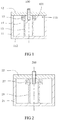
- FIG. 1 is a cutaway diagram of a resonator 100.
- the resonator 100 includes: a resonant cavity casing 11, a cover 12, a resonance tube 13, and a tuning screw 14.
- the resonant cavity casing 11 is a metal cavity casing
- the resonant cavity casing 11 may be a cavity casing that is entirely made of a metal material or that is metalized at least on an inner surface
- the resonant cavity casing 11 has a resonant cavity 112 and an open end 113.
- the cover 12 covers the open end 113 and is connected to the resonant cavity casing 11, and a connection manner of the cover 12 and the resonant cavity casing 11 may be connecting by using a screw, or the like.
- the cover 12 may be an independent component, or may be a PCB (printed circuit board). When the PCB is mounted on the resonant cavity casing 11 in a fastened manner and covers the open end 113, the PCB is used as the cover 12.
- the resonance tube 13 is located inside the resonant cavity 112.
- the resonance tube 13 is integrated with the resonant cavity casing 11 as one casing, that is, the resonance tube 13 is integrated on an inner side surface of the bottom of the resonant cavity casing 11 as one casing.
- the resonance tube 13 may be an independently disposed component, and is connected to the resonant cavity casing 11 in a fastened manner by using a fastening element.
- the tuning screw 14 is connected to the cover 12 and stretches into the resonance tube 13, and a length of a part that is of the tuning screw 14 and that stretches into the resonance tube 13 is changed by rotating the tuning screw 14, so that frequency may be adjusted.
- the tuning screw 14 and the resonance tube 13 are coaxially disposed.
- the resonator 100 further includes a dielectric material 17 that is filled in the resonant cavity 112 and whose dielectric constant is greater than 1.
- the dielectric material 17 is filled in a capacitance area formed between the top of the resonance tube 13 and the cover 12.
- An upper end surface and a lower end surface of the dielectric material 17 respectively are in contact with a lower surface of the cover 12 and an upper surface of the resonance tube 13.
- the capacitance area specifically includes at least one of an area between the resonance tube 13 and the cover 12, an area between the tuning screw 14 and an inner wall of the resonance tube 13, or an area between an outer edge of the resonance tube 13 and a cavity wall of the resonant cavity 112. These areas have greater electric intensity than another area inside the resonant cavity casing, that is, these areas have relatively high electric intensity.
- the dielectric material 17 may be tightly in contact with the cover 12 and the resonance tube 13, that is, an air gap between the dielectric material 17 and the lower surface of the cover 12 is less than 0.2 mm, and an air gap between the dielectric material 17 and the upper surface of the resonance tube 13 is less than 0.2 mm.
- the dielectric material 17 includes but is not limited to: ceramic, monocrystalline quartz, or spherical alumina.
- the top of the resonance tube 13 of the resonator 100 may have a disc 131 that extends outwards, and the dielectric material 17 is filled between the cover 12 and the disc 131.
- a filling volume of the dielectric material 17 can be increased; or in the case of a same volume of the dielectric material 17, a decrease in a height of the dielectric material 17 helps reduce an entire volume of the resonator 100.
- the filled dielectric material 17 is separately fastened to the cover 12 and the resonance tube 13 by means of bonding or welding.
- a quality factor Qf of the dielectric material 17 is greater than 5000, to reduce a dielectric loss.
- the quality factor is a reciprocal of the dielectric loss of the dielectric material 17. Because the low-loss dielectric material 17 may be filled, a loss of the dielectric material 17 can be lower in a case in which the resonator 100 in this implementation manner has a same resonant cavity volume as an SIR resonator (stepped-impedance resonator, Stepped Impedance Resonator), and an increase in the dielectric loss brought by the filled dielectric material can be less than a decrease in a conductor loss; therefore, a loss of the resonator 100 provided in this embodiment of the present invention is less than that in an SIR technology.
- Beneficial effects generated by the resonator 100 are as follows:
- FIG. 2 is a cutaway diagram of a resonator 200.
- the resonator 200 is basically similar to the resonator 100 shown in FIG. 1 , and a difference between the resonator 200 and the resonator 100 lies in that the filled dielectric material 27 is crimped between the cover 22 and the resonance tube 23.
- An implementation manner of the resonator 200 may be as follows: A thickness of the dielectric material 27 is properly set; when the cover 22 is mounted on the resonant cavity casing 21 in a fastened manner, the cover 22 presses against the dielectric material 27; the dielectric material 27 is tightly crimped between the cover 22 and the resonance tube 23. By using this mounting manner, mounting of the dielectric material 27 can be facilitated.
- FIG. 3 is a cutaway diagram of a resonator 300.
- the resonator 300 is basically similar to the resonator 100 shown in FIG. 1 , and a difference between the resonator 300 and the resonator 100 lies in that the resonance tube 33 is a post, a disc is not formed on the top of the resonance tube 33, and an upper surface and a lower surface of the dielectric material 37 is respectively fastened to the cover 32 and the resonance tube 33 by means of bonding.
- the resonance tube 33 is a post
- a disc is not formed on the top of the resonance tube 33
- an upper surface and a lower surface of the dielectric material 37 is respectively fastened to the cover 32 and the resonance tube 33 by means of bonding.
- FIG. 4 is a cutaway diagram of a resonator 400.
- the resonator 400 is basically similar to the resonator 200 shown in FIG. 2 , and a difference between the resonator 400 and the resonator 200 lies in that the resonance tube 43 is a post, a disc is not formed on the top of the resonance tube 43, and the dielectric material 47 is crimped between the cover 42 and the resonance tube 43.
- FIG. 5 and FIG. 6 respectively are a three-dimensional cutaway diagram and a three-dimensional exploded diagram of a filter 500.
- the filter 500 is constructed by combining multiple foregoing resonators.
- the filter 500 in this implementation manner includes three resonators that are arranged at an interval, and cover of the three resonators are integrated and resonant cavity casings that are of resonators located on the periphery of the filter are integrated; therefore, the filter 500 includes a case 51 and a cover 52 that covers the case 51.
- the case 51 is a metal case
- the cover 52 is a metal cover
- the case 51 may be a cavity casing that is entirely made of a metal material or that is metalized at least on an inner surface
- the metal cover 52 may be a plate casing that is entirely made of a metal material or that is metalized at least on a lower surface.
- the filter 500 is a three-cavity filter.
- the case 51 has an open end and three resonant cavities 512.
- the cover 52 covers the open end.
- a resonance tube 53 and a tuning screw 54 corresponding to the resonant cavity 512 are disposed inside each resonant cavity 512.
- An area with relatively high electric intensity inside each resonant cavity 512 is filled with a dielectric material 57.
- a filling area and a filling manner for the dielectric material 57 are any one applied to the resonator in the first implementation manner to the fourth implementation manner.
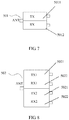
- FIG. 7 is a schematic structural diagram of a duplexer 501.
- the duplexer 501 includes a transmitter channel filter 5011 and a receiver channel filter 5012, where the transmitter channel filter 5011 and the receiver channel filter 5012 perform filtering by using the foregoing filter 500.
- the transmitter channel filter 5011 is configured to process a transmit signal of a transmitter
- the receiver channel filter 5012 is configured to process a receive signal of a receiver.
- FIG. 8 is a schematic structural diagram of a multiplexer 502
- the multiplexer 502 includes multiple transmitter channel filters 5021 and multiple receiver channel filters 5022, where the transmitter channel filters 5021 and the receiver channel filters 5022 perform filtering by using the foregoing filter 500.
- the figure shows two transmitter channel filters 5021 and two receiver channel filters 5022, and there may be three or more transmitter channel filters and receiver channel filters in another implementation manner.
- the transmitter channel filter 5021 is configured to process a transmit signal of a transmitter
- the receiver channel filter 5022 is configured to process a receive signal of a receiver.
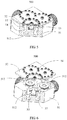
- FIG. 9 is a three-dimensional cutaway diagram of a resonator 600 according to an implementation manner of the present invention.
- FIG. 10 is a full cutaway diagram of the resonator 600 according to the implementation manner of the present invention.
- the resonator 600 includes: a resonant cavity casing 61, a cover 62, a resonance tube 63, and a tuning rod 64.
- the resonant cavity casing 61 is a metal cavity casing
- the resonant cavity casing 61 may be a cavity casing that is entirely made of a metal material or that is metalized at least on an inner surface
- the resonant cavity casing 61 has a resonant cavity 612 and an open end 613.
- the cover 62 covers the open end 613 and is connected to the resonant cavity casing 61, and a connection manner of the cover 62 and the resonant cavity casing 61 may be connecting by using a screw, or the like.
- the cover 62 may be an independent component, or may be a PCB. When the PCB is mounted on the resonant cavity casing 61 in a fastened manner and covers the open end 613, the PCB is used as the cover 62.
- the resonance tube 63 is located inside the resonant cavity 612.
- the resonance tube 63 is integrated with the resonant cavity casing 61 as one casing, that is, the resonance tube 63 is integrated on an inner surface of the bottom of the resonant cavity casing 61 as one casing.
- a circular via hole is disposed at the center of the resonance tube 63.
- the resonance tube 63 may be an independently disposed component, and is connected to the resonant cavity casing 61 in a fastened manner by using a fastening element.
- the fastening element plays a role of fastening the resonance tube 63, and the fastening element may be made of a metal piece or may be made of another material.
- the resonator 600 further includes a dielectric material 67 that is filled in the resonant cavity 612 and whose dielectric constant is greater than 1.
- the dielectric material 67 is filled in a capacitance area formed between the top of the resonance tube 63 and the cover 62.
- the capacitance area may include: an area between a top surface of the resonance tube 63 and a lower surface of the cover 62, or an area between the top of a cavity casing encircled by an inner wall of the resonance tube 63 and a lower surface of the cover 62.
- the capacitance area has greater electric intensity than another area inside the resonant cavity casing 612, that is, this area has relatively high electric intensity.
- the tuning rod 64 is rotatable relative to the dielectric material 67, and a contact surface of the tuning rod 64 and the dielectric material 67 is in a non-circular structure, so that the tuning rod 64 can adjust the frequency when being rotated relative to the dielectric material 67.
- the non-circular structure refers to a circle with an incomplete cross section, such as a quadrilateral, a sector, or a circle with a gap.
- an upper surface of the filled dielectric material 67 is in contact with the lower surface of the cover 62, and a lower surface of the filled dielectric material 67 is in contact with or not in contact with an upper surface of the top of the tuning rod.
- the upper surface of the dielectric material 67 is fastened to the lower surface of the cover 62 by means of welding or bonding.
- the tuning rod 64 includes a main part 641 inserted inside the resonance tube 63, and a resonant disc 642 formed on the top of the main part 641.
- the resonant disc 642 is located between the main part 641 and the cover 62, and protrudes from the top of the resonance tube 63.
- a diameter of the resonant disc 642 is greater than an outer diameter of the resonance tube 63.
- the dielectric material 67 is filled between the resonant disc 642 and the cover 62.
- Disposing of the resonant disc 642 helps increase an area of contact between the resonant disc 642 and the dielectric material 67, to increase a volume of the dielectric material 67; or in the case of a same volume of the dielectric material 67, a decrease in a height of the dielectric material 67 helps reduce an entire volume of the resonator 600.
- the resonator 600 further includes a base plate 65 connected to the bottom of the resonant cavity casing, and an elastic element 66 pushing against the base plate 65 and the tuning rod 64.
- the elastic element 66 provides elastic pressure for the tuning rod 64 to press against the dielectric material 67.
- the elastic element 66 may be a spring.
- the elastic element 66 is disposed, and when a frequency needs to be re-adjusted, the base plate 65 may be released, and after the tuning rod 64 is separated from the dielectric material 67, adjustment is performed.
- the base plate 65 is connected to a base plate of the resonant cavity casing 61, where a connection manner of the base plate 65 and the resonant cavity casing 61 may be connecting by using a screw, or may be another manner, which is not limited herein.
- the screw plays a role of connecting the base plate 65 and the resonant cavity casing 61, where a metal screw may be used, or a screw made of another material may be used.
- the resonator 600 further includes a tuning screw 68, where the tuning screw 68 is configured to adjust rotation of the tuning rod 64.
- the tuning screw 68 penetrates the base plate 65 and is connected to the tuning rod 64 in a fastened manner.
- the tuning screw 68 is rotated by using a tool, for example, a screwdriver, the tuning rod 64 may be driven to rotate, to change a relative position between the tuning rod 64 and the dielectric material 67, that is, to adjust a position at which the tuning rod 64 and the dielectric material 67 mutually overlap, so as to adjust a frequency.
- Using of the tuning screw 68 may help perform fine adjustment and multiple times of adjustment.
- the tuning screw 68 may not be disposed to perform frequency adjustment; instead, after the relative position between the tuning rod 64 and the dielectric material 67 is adjusted to achieve a required frequency, a position of the tuning rod is fastened by means of dispensing.
- a grounding protrusion part 644 that remains to be connected to an inner side wall of the resonance tube 63 is disposed on a side surface of the tuning rod 64.
- the tuning rod 64 remains to be connected to the inner wall of the resonance tube 63 by using the grounding protrusion part 644.
- the grounding protrusion part 644 is a torus encircling the main part 641.
- the resonance tube 63 may be grounded in another manner. For example, grounding is implemented by using a ground point at the bottom.
- a shape of the contact surface of the tuning rod 64 and the dielectric material 67 is a quadrilateral, that is, both the resonant disc 642 and the dielectric material 67 are quadrilaterals.
- a shape of the contact surface of the tuning rod 64 and the dielectric material 67 is a sector, that is, both the resonant disc 642 and the dielectric material 67 are sectors.
- a shape of the contact surface of the tuning rod 64 and the dielectric material 67 is a round rectangle, that is, both the resonant disc 642 and the dielectric material 67 are round rectangles.
- a shape of the contact surface of the tuning rod 64 and the dielectric material 67 may be a circle in which a defect part is provided, for example, a circle in which a regular or an irregular gap is provided, or a circle in which a via hole is provided on a surface.
- the foregoing shape of the contact surface of the tuning rod 64 and the dielectric material 67 may be selected according to convenience of a manufacturing technique.
- the resonator 600 in this implementation manner of the present invention has the following beneficial technical effects:
- An implementation manner of the present invention further provides a filter (not shown in the diagrams), including the foregoing resonator 600.
- An implementation manner of the present invention further provides a duplexer (not shown in the diagrams), including a transmitter channel filter and a receiver channel filter, where the transmitter channel filter and the receiver channel filter perform filtering by using the foregoing filter 600.
- the transmitter channel filter is configured to process a transmit signal of a transmitter
- the receiver channel filter is configured to process a receive signal of a receiver.
- An implementation manner of the present invention further provides a multiplexer (not shown in the diagrams), including multiple transmitter channel filters and multiple receiver channel filters, where the transmitter channel filters and the receiver channel filters perform filtering by using the foregoing filter 600.
- the filter, the duplexer, and the multiplexer provided in the foregoing embodiments may be applied to a communications system, or may be applied to a radar system, which may not be limited herein.
Landscapes
- Control Of Motors That Do Not Use Commutators (AREA)
Applications Claiming Priority (1)
| Application Number | Priority Date | Filing Date | Title |
|---|---|---|---|
| PCT/CN2013/087304 WO2015070450A1 (zh) | 2013-11-18 | 2013-11-18 | 谐振器、滤波器、双工器及多工器 |
Publications (3)
| Publication Number | Publication Date |
|---|---|
| EP3062386A1 EP3062386A1 (en) | 2016-08-31 |
| EP3062386A4 EP3062386A4 (en) | 2016-12-21 |
| EP3062386B1 true EP3062386B1 (en) | 2020-05-20 |
Family
ID=51912354
Family Applications (1)
| Application Number | Title | Priority Date | Filing Date |
|---|---|---|---|
| EP13897663.4A Active EP3062386B1 (en) | 2013-11-18 | 2013-11-18 | Resonator, filter, duplexer and multiplexer |
Country Status (5)
| Country | Link |
|---|---|
| US (1) | US10096884B2 (sv) |
| EP (1) | EP3062386B1 (sv) |
| CN (1) | CN104170162B (sv) |
| BR (1) | BR112016011287B1 (sv) |
| WO (1) | WO2015070450A1 (sv) |
Families Citing this family (16)
| Publication number | Priority date | Publication date | Assignee | Title |
|---|---|---|---|---|
| CN104953206B (zh) * | 2015-06-23 | 2018-02-13 | 上海航天测控通信研究所 | 一种同轴腔体滤波器及其介质填充方法 |
| CN105633520B (zh) * | 2016-03-01 | 2018-09-21 | 西南交通大学 | 一种双频窄带带通介质滤波器 |
| CN106129574A (zh) * | 2016-08-25 | 2016-11-16 | 安徽华东光电技术研究所 | 腔体滤波器及其制备方法 |
| WO2018119825A1 (zh) * | 2016-12-29 | 2018-07-05 | 深圳市大富科技股份有限公司 | 一种tem模滤波器及通信设备 |
| US10177431B2 (en) * | 2016-12-30 | 2019-01-08 | Nokia Shanghai Bell Co., Ltd. | Dielectric loaded metallic resonator |
| CN110168802B (zh) | 2017-01-18 | 2021-07-20 | 华为技术有限公司 | 一种横磁模介质谐振器、滤波器及通信设备 |
| CN109962325A (zh) * | 2017-12-22 | 2019-07-02 | 香港凡谷發展有限公司 | 一种全介质混合谐振结构及滤波器 |
| CN110364788B (zh) * | 2018-04-11 | 2021-05-18 | 上海华为技术有限公司 | 滤波装置 |
| CN108987863A (zh) * | 2018-09-18 | 2018-12-11 | 苏州市协诚五金制品有限公司 | 一种双零点交叉耦合陶瓷滤波器 |
| CN109216839B (zh) * | 2018-09-28 | 2024-03-22 | 西南应用磁学研究所 | 一种新型小型化交指陶瓷管介质腔体滤波器 |
| RU190739U1 (ru) * | 2019-04-26 | 2019-07-11 | Акционерное общество "Научно-исследовательский институт Приборостроения имени В.В. Тихомирова" | СВЧ смеситель |
| CN110247142B (zh) * | 2019-06-27 | 2021-05-18 | 深圳大学 | 滤波器 |
| CN110875506B (zh) * | 2019-12-02 | 2021-07-13 | 成都雷电微力科技股份有限公司 | 一种紧凑型介质填充波导滤波器 |
| CN113224487A (zh) * | 2020-01-21 | 2021-08-06 | 深圳市大富科技股份有限公司 | 5g无线通信基站 |
| CN112002971A (zh) * | 2020-09-01 | 2020-11-27 | 苏州诺泰信通讯有限公司 | 一种含有填充介质的滤波器 |
| WO2023273032A1 (zh) * | 2021-06-29 | 2023-01-05 | 大富科技(安徽)股份有限公司 | 谐振器、滤波器、双工器、多工器以及通信设备 |
Family Cites Families (20)
| Publication number | Priority date | Publication date | Assignee | Title |
|---|---|---|---|---|
| US4024481A (en) * | 1976-01-07 | 1977-05-17 | International Telephone And Telegraph Corporation | Frequency drift compensation due to temperature variations in dielectric loaded cavity filters |
| JPS57124902A (en) * | 1981-01-26 | 1982-08-04 | Toyo Commun Equip Co Ltd | Filter for semicoaxial cavity resonator |
| US4728913A (en) * | 1985-01-18 | 1988-03-01 | Murata Manufacturing Co., Ltd. | Dielectric resonator |
| US4963841A (en) * | 1989-05-25 | 1990-10-16 | Raytheon Company | Dielectric resonator filter |
| US6147577A (en) * | 1998-01-15 | 2000-11-14 | K&L Microwave, Inc. | Tunable ceramic filters |
| JP3241671B2 (ja) | 1998-11-30 | 2001-12-25 | 日本電気株式会社 | 高周波誘電体濾波器 |
| US6255917B1 (en) | 1999-01-12 | 2001-07-03 | Teledyne Technologies Incorporated | Filter with stepped impedance resonators and method of making the filter |
| SE519554C2 (sv) | 1999-04-14 | 2003-03-11 | Ericsson Telefon Ab L M | Skruvanordning samt trimanordning innefattande en sådan skruvanordning för trimning av ett kavitetsfilters frekvensförhållande eller kopplingsgrad |
| US6222428B1 (en) * | 1999-06-15 | 2001-04-24 | Allgon Ab | Tuning assembly for a dielectrical resonator in a cavity |
| JP3506121B2 (ja) | 2000-03-30 | 2004-03-15 | 株式会社村田製作所 | 誘電体共振器、フィルタ、デュプレクサおよび通信装置 |
| FI119207B (sv) * | 2003-03-18 | 2008-08-29 | Filtronic Comtek Oy | Koaxialresonatorfilter |
| US6904666B2 (en) | 2003-07-31 | 2005-06-14 | Andrew Corporation | Method of manufacturing microwave filter components and microwave filter components formed thereby |
| CN1273408C (zh) * | 2004-03-23 | 2006-09-06 | 浙江大学 | 低温烧结(Ca,Mg)SiO3系微波介质陶瓷及制备工艺 |
| US20060284708A1 (en) * | 2005-06-15 | 2006-12-21 | Masions Of Thought, R&D, L.L.C. | Dielectrically loaded coaxial resonator |
| GB2452293B (en) * | 2007-08-30 | 2011-09-28 | Isotek Electronics Ltd | A tuneable filter and a method of tuning such a filter |
| EP2099091B1 (en) | 2008-03-04 | 2017-11-22 | HMD global Oy | Variable radio frequency band filter |
| WO2013036485A1 (en) * | 2011-09-06 | 2013-03-14 | Powerwave Technologies | Open circuit common junction feed for duplexer |
| CN103311633B (zh) * | 2012-03-15 | 2015-03-11 | 成都赛纳赛德科技有限公司 | 一种谐振器调谐结构 |
| CN102903987A (zh) * | 2012-10-18 | 2013-01-30 | 江苏贝孚德通讯科技股份有限公司 | 金属同轴滤波器 |
| CN103022621A (zh) * | 2012-12-18 | 2013-04-03 | 四川九洲电器集团有限责任公司 | 运用介质块加载的谐振器 |
-
2013
- 2013-11-18 WO PCT/CN2013/087304 patent/WO2015070450A1/zh active Application Filing
- 2013-11-18 EP EP13897663.4A patent/EP3062386B1/en active Active
- 2013-11-18 CN CN201380004298.7A patent/CN104170162B/zh active Active
- 2013-11-18 BR BR112016011287-3A patent/BR112016011287B1/pt active IP Right Grant
-
2016
- 2016-05-16 US US15/156,137 patent/US10096884B2/en active Active
Non-Patent Citations (1)
| Title |
|---|
| None * |
Also Published As
| Publication number | Publication date |
|---|---|
| CN104170162A (zh) | 2014-11-26 |
| EP3062386A1 (en) | 2016-08-31 |
| US10096884B2 (en) | 2018-10-09 |
| BR112016011287A2 (sv) | 2017-08-08 |
| WO2015070450A1 (zh) | 2015-05-21 |
| EP3062386A4 (en) | 2016-12-21 |
| US20160261018A1 (en) | 2016-09-08 |
| CN104170162B (zh) | 2017-02-15 |
| BR112016011287B1 (pt) | 2022-03-15 |
Similar Documents
| Publication | Publication Date | Title |
|---|---|---|
| EP3062386B1 (en) | Resonator, filter, duplexer and multiplexer | |
| US9979070B2 (en) | Resonator, filter, duplexer, multiplexer, and communications device | |
| US10873119B2 (en) | Filter and wireless network device | |
| CN110098453B (zh) | 射频滤波器 | |
| US9236846B2 (en) | Tunable bandpass filter device and method | |
| CN102324602A (zh) | 用于TE01δ模介质谐振器的电感耦合装置 | |
| CN107210510B (zh) | 介质谐振器及滤波器 | |
| CN106960994A (zh) | 一种便于调节频率与耦合带宽的介质滤波器 | |
| CN104979609A (zh) | 腔体滤波器 | |
| CN206864583U (zh) | 一种便于调节频率与耦合带宽的介质滤波器 | |
| EP3217468B1 (en) | Transverse electromagnetic mode dielectric filter, radio frequency module and base station | |
| EP3561948B1 (en) | Cavity resonator, filter and communication device | |
| US11108123B2 (en) | Triple-mode dielectric resonator filter, method for manufacturing the same, and band pass filter using dielectric resonator and NRN stub | |
| EP3553880A1 (en) | Resonator and communication device | |
| EP3384551B1 (en) | Coaxial resonator with dielectric disc | |
| CN204668441U (zh) | 频率间距可调的双模介质谐振装置 | |
| WO2017054474A1 (zh) | 一种谐振腔及滤波器 | |
| CN115483522A (zh) | 一种金属谐振器 | |
| CN107112616A (zh) | 一种介质滤波器 | |
| KR20100008939A (ko) | 감쇄 특성을 향상시킨 일체형 유전체 필터 및 이를 이용한통신 중계 장치 | |
| CN207265203U (zh) | 一种介质滤波器及通信设备 | |
| CN103855454A (zh) | 一种谐振腔、滤波器件及电磁波设备 | |
| CN218770035U (zh) | 一种金属谐振器 | |
| CN211743359U (zh) | 一种介质分层式的滤波器 | |
| CN114204236B (zh) | 一种大频率比的腔体双频宽带滤波器 |
Legal Events
| Date | Code | Title | Description |
|---|---|---|---|
| PUAI | Public reference made under article 153(3) epc to a published international application that has entered the european phase |
Free format text: ORIGINAL CODE: 0009012 |
|
| 17P | Request for examination filed |
Effective date: 20160525 |
|
| AK | Designated contracting states |
Kind code of ref document: A1 Designated state(s): AL AT BE BG CH CY CZ DE DK EE ES FI FR GB GR HR HU IE IS IT LI LT LU LV MC MK MT NL NO PL PT RO RS SE SI SK SM TR |
|
| AX | Request for extension of the european patent |
Extension state: BA ME |
|
| A4 | Supplementary search report drawn up and despatched |
Effective date: 20161122 |
|
| RIC1 | Information provided on ipc code assigned before grant |
Ipc: H01P 7/04 20060101AFI20161116BHEP Ipc: H01P 7/06 20060101ALI20161116BHEP |
|
| DAX | Request for extension of the european patent (deleted) | ||
| STAA | Information on the status of an ep patent application or granted ep patent |
Free format text: STATUS: EXAMINATION IS IN PROGRESS |
|
| 17Q | First examination report despatched |
Effective date: 20190222 |
|
| GRAP | Despatch of communication of intention to grant a patent |
Free format text: ORIGINAL CODE: EPIDOSNIGR1 |
|
| STAA | Information on the status of an ep patent application or granted ep patent |
Free format text: STATUS: GRANT OF PATENT IS INTENDED |
|
| INTG | Intention to grant announced |
Effective date: 20191206 |
|
| GRAS | Grant fee paid |
Free format text: ORIGINAL CODE: EPIDOSNIGR3 |
|
| GRAA | (expected) grant |
Free format text: ORIGINAL CODE: 0009210 |
|
| STAA | Information on the status of an ep patent application or granted ep patent |
Free format text: STATUS: THE PATENT HAS BEEN GRANTED |
|
| AK | Designated contracting states |
Kind code of ref document: B1 Designated state(s): AL AT BE BG CH CY CZ DE DK EE ES FI FR GB GR HR HU IE IS IT LI LT LU LV MC MK MT NL NO PL PT RO RS SE SI SK SM TR |
|
| REG | Reference to a national code |
Ref country code: GB Ref legal event code: FG4D |
|
| REG | Reference to a national code |
Ref country code: CH Ref legal event code: EP |
|
| REG | Reference to a national code |
Ref country code: DE Ref legal event code: R096 Ref document number: 602013069332 Country of ref document: DE |
|
| REG | Reference to a national code |
Ref country code: AT Ref legal event code: REF Ref document number: 1273222 Country of ref document: AT Kind code of ref document: T Effective date: 20200615 |
|
| REG | Reference to a national code |
Ref country code: LT Ref legal event code: MG4D |
|
| REG | Reference to a national code |
Ref country code: NL Ref legal event code: MP Effective date: 20200520 |
|
| PG25 | Lapsed in a contracting state [announced via postgrant information from national office to epo] |
Ref country code: PT Free format text: LAPSE BECAUSE OF FAILURE TO SUBMIT A TRANSLATION OF THE DESCRIPTION OR TO PAY THE FEE WITHIN THE PRESCRIBED TIME-LIMIT Effective date: 20200921 Ref country code: IS Free format text: LAPSE BECAUSE OF FAILURE TO SUBMIT A TRANSLATION OF THE DESCRIPTION OR TO PAY THE FEE WITHIN THE PRESCRIBED TIME-LIMIT Effective date: 20200920 Ref country code: NO Free format text: LAPSE BECAUSE OF FAILURE TO SUBMIT A TRANSLATION OF THE DESCRIPTION OR TO PAY THE FEE WITHIN THE PRESCRIBED TIME-LIMIT Effective date: 20200820 Ref country code: GR Free format text: LAPSE BECAUSE OF FAILURE TO SUBMIT A TRANSLATION OF THE DESCRIPTION OR TO PAY THE FEE WITHIN THE PRESCRIBED TIME-LIMIT Effective date: 20200821 Ref country code: FI Free format text: LAPSE BECAUSE OF FAILURE TO SUBMIT A TRANSLATION OF THE DESCRIPTION OR TO PAY THE FEE WITHIN THE PRESCRIBED TIME-LIMIT Effective date: 20200520 Ref country code: SE Free format text: LAPSE BECAUSE OF FAILURE TO SUBMIT A TRANSLATION OF THE DESCRIPTION OR TO PAY THE FEE WITHIN THE PRESCRIBED TIME-LIMIT Effective date: 20200520 Ref country code: LT Free format text: LAPSE BECAUSE OF FAILURE TO SUBMIT A TRANSLATION OF THE DESCRIPTION OR TO PAY THE FEE WITHIN THE PRESCRIBED TIME-LIMIT Effective date: 20200520 |
|
| PG25 | Lapsed in a contracting state [announced via postgrant information from national office to epo] |
Ref country code: BG Free format text: LAPSE BECAUSE OF FAILURE TO SUBMIT A TRANSLATION OF THE DESCRIPTION OR TO PAY THE FEE WITHIN THE PRESCRIBED TIME-LIMIT Effective date: 20200820 Ref country code: RS Free format text: LAPSE BECAUSE OF FAILURE TO SUBMIT A TRANSLATION OF THE DESCRIPTION OR TO PAY THE FEE WITHIN THE PRESCRIBED TIME-LIMIT Effective date: 20200520 Ref country code: LV Free format text: LAPSE BECAUSE OF FAILURE TO SUBMIT A TRANSLATION OF THE DESCRIPTION OR TO PAY THE FEE WITHIN THE PRESCRIBED TIME-LIMIT Effective date: 20200520 Ref country code: HR Free format text: LAPSE BECAUSE OF FAILURE TO SUBMIT A TRANSLATION OF THE DESCRIPTION OR TO PAY THE FEE WITHIN THE PRESCRIBED TIME-LIMIT Effective date: 20200520 |
|
| REG | Reference to a national code |
Ref country code: AT Ref legal event code: MK05 Ref document number: 1273222 Country of ref document: AT Kind code of ref document: T Effective date: 20200520 |
|
| PG25 | Lapsed in a contracting state [announced via postgrant information from national office to epo] |
Ref country code: NL Free format text: LAPSE BECAUSE OF FAILURE TO SUBMIT A TRANSLATION OF THE DESCRIPTION OR TO PAY THE FEE WITHIN THE PRESCRIBED TIME-LIMIT Effective date: 20200520 Ref country code: AL Free format text: LAPSE BECAUSE OF FAILURE TO SUBMIT A TRANSLATION OF THE DESCRIPTION OR TO PAY THE FEE WITHIN THE PRESCRIBED TIME-LIMIT Effective date: 20200520 |
|
| PG25 | Lapsed in a contracting state [announced via postgrant information from national office to epo] |
Ref country code: AT Free format text: LAPSE BECAUSE OF FAILURE TO SUBMIT A TRANSLATION OF THE DESCRIPTION OR TO PAY THE FEE WITHIN THE PRESCRIBED TIME-LIMIT Effective date: 20200520 Ref country code: SM Free format text: LAPSE BECAUSE OF FAILURE TO SUBMIT A TRANSLATION OF THE DESCRIPTION OR TO PAY THE FEE WITHIN THE PRESCRIBED TIME-LIMIT Effective date: 20200520 Ref country code: EE Free format text: LAPSE BECAUSE OF FAILURE TO SUBMIT A TRANSLATION OF THE DESCRIPTION OR TO PAY THE FEE WITHIN THE PRESCRIBED TIME-LIMIT Effective date: 20200520 Ref country code: DK Free format text: LAPSE BECAUSE OF FAILURE TO SUBMIT A TRANSLATION OF THE DESCRIPTION OR TO PAY THE FEE WITHIN THE PRESCRIBED TIME-LIMIT Effective date: 20200520 Ref country code: RO Free format text: LAPSE BECAUSE OF FAILURE TO SUBMIT A TRANSLATION OF THE DESCRIPTION OR TO PAY THE FEE WITHIN THE PRESCRIBED TIME-LIMIT Effective date: 20200520 Ref country code: CZ Free format text: LAPSE BECAUSE OF FAILURE TO SUBMIT A TRANSLATION OF THE DESCRIPTION OR TO PAY THE FEE WITHIN THE PRESCRIBED TIME-LIMIT Effective date: 20200520 Ref country code: ES Free format text: LAPSE BECAUSE OF FAILURE TO SUBMIT A TRANSLATION OF THE DESCRIPTION OR TO PAY THE FEE WITHIN THE PRESCRIBED TIME-LIMIT Effective date: 20200520 |
|
| REG | Reference to a national code |
Ref country code: DE Ref legal event code: R097 Ref document number: 602013069332 Country of ref document: DE |
|
| PG25 | Lapsed in a contracting state [announced via postgrant information from national office to epo] |
Ref country code: PL Free format text: LAPSE BECAUSE OF FAILURE TO SUBMIT A TRANSLATION OF THE DESCRIPTION OR TO PAY THE FEE WITHIN THE PRESCRIBED TIME-LIMIT Effective date: 20200520 Ref country code: SK Free format text: LAPSE BECAUSE OF FAILURE TO SUBMIT A TRANSLATION OF THE DESCRIPTION OR TO PAY THE FEE WITHIN THE PRESCRIBED TIME-LIMIT Effective date: 20200520 |
|
| PLBE | No opposition filed within time limit |
Free format text: ORIGINAL CODE: 0009261 |
|
| STAA | Information on the status of an ep patent application or granted ep patent |
Free format text: STATUS: NO OPPOSITION FILED WITHIN TIME LIMIT |
|
| 26N | No opposition filed |
Effective date: 20210223 |
|
| PG25 | Lapsed in a contracting state [announced via postgrant information from national office to epo] |
Ref country code: SI Free format text: LAPSE BECAUSE OF FAILURE TO SUBMIT A TRANSLATION OF THE DESCRIPTION OR TO PAY THE FEE WITHIN THE PRESCRIBED TIME-LIMIT Effective date: 20200520 |
|
| PG25 | Lapsed in a contracting state [announced via postgrant information from national office to epo] |
Ref country code: MC Free format text: LAPSE BECAUSE OF FAILURE TO SUBMIT A TRANSLATION OF THE DESCRIPTION OR TO PAY THE FEE WITHIN THE PRESCRIBED TIME-LIMIT Effective date: 20200520 |
|
| REG | Reference to a national code |
Ref country code: CH Ref legal event code: PL |
|
| PG25 | Lapsed in a contracting state [announced via postgrant information from national office to epo] |
Ref country code: LU Free format text: LAPSE BECAUSE OF NON-PAYMENT OF DUE FEES Effective date: 20201118 |
|
| REG | Reference to a national code |
Ref country code: BE Ref legal event code: MM Effective date: 20201130 |
|
| PG25 | Lapsed in a contracting state [announced via postgrant information from national office to epo] |
Ref country code: LI Free format text: LAPSE BECAUSE OF NON-PAYMENT OF DUE FEES Effective date: 20201130 Ref country code: CH Free format text: LAPSE BECAUSE OF NON-PAYMENT OF DUE FEES Effective date: 20201130 |
|
| PG25 | Lapsed in a contracting state [announced via postgrant information from national office to epo] |
Ref country code: IE Free format text: LAPSE BECAUSE OF NON-PAYMENT OF DUE FEES Effective date: 20201118 Ref country code: FR Free format text: LAPSE BECAUSE OF NON-PAYMENT OF DUE FEES Effective date: 20201130 |
|
| PG25 | Lapsed in a contracting state [announced via postgrant information from national office to epo] |
Ref country code: TR Free format text: LAPSE BECAUSE OF FAILURE TO SUBMIT A TRANSLATION OF THE DESCRIPTION OR TO PAY THE FEE WITHIN THE PRESCRIBED TIME-LIMIT Effective date: 20200520 Ref country code: MT Free format text: LAPSE BECAUSE OF FAILURE TO SUBMIT A TRANSLATION OF THE DESCRIPTION OR TO PAY THE FEE WITHIN THE PRESCRIBED TIME-LIMIT Effective date: 20200520 Ref country code: CY Free format text: LAPSE BECAUSE OF FAILURE TO SUBMIT A TRANSLATION OF THE DESCRIPTION OR TO PAY THE FEE WITHIN THE PRESCRIBED TIME-LIMIT Effective date: 20200520 |
|
| PG25 | Lapsed in a contracting state [announced via postgrant information from national office to epo] |
Ref country code: MK Free format text: LAPSE BECAUSE OF FAILURE TO SUBMIT A TRANSLATION OF THE DESCRIPTION OR TO PAY THE FEE WITHIN THE PRESCRIBED TIME-LIMIT Effective date: 20200520 |
|
| PG25 | Lapsed in a contracting state [announced via postgrant information from national office to epo] |
Ref country code: BE Free format text: LAPSE BECAUSE OF NON-PAYMENT OF DUE FEES Effective date: 20201130 |
|
| PGFP | Annual fee paid to national office [announced via postgrant information from national office to epo] |
Ref country code: GB Payment date: 20231006 Year of fee payment: 11 |
|
| PGFP | Annual fee paid to national office [announced via postgrant information from national office to epo] |
Ref country code: IT Payment date: 20231010 Year of fee payment: 11 Ref country code: DE Payment date: 20230929 Year of fee payment: 11 |