EP3217468B1 - Transverse electromagnetic mode dielectric filter, radio frequency module and base station - Google Patents
Transverse electromagnetic mode dielectric filter, radio frequency module and base station Download PDFInfo
- Publication number
- EP3217468B1 EP3217468B1 EP15867903.5A EP15867903A EP3217468B1 EP 3217468 B1 EP3217468 B1 EP 3217468B1 EP 15867903 A EP15867903 A EP 15867903A EP 3217468 B1 EP3217468 B1 EP 3217468B1
- Authority
- EP
- European Patent Office
- Prior art keywords
- filter
- dielectric body
- resonant
- rejection structure
- frequency
- Prior art date
- Legal status (The legal status is an assumption and is not a legal conclusion. Google has not performed a legal analysis and makes no representation as to the accuracy of the status listed.)
- Active
Links
Images

Classifications
-
- H—ELECTRICITY
- H01—ELECTRIC ELEMENTS
- H01P—WAVEGUIDES; RESONATORS, LINES, OR OTHER DEVICES OF THE WAVEGUIDE TYPE
- H01P1/00—Auxiliary devices
- H01P1/20—Frequency-selective devices, e.g. filters
- H01P1/201—Filters for transverse electromagnetic waves
- H01P1/205—Comb or interdigital filters; Cascaded coaxial cavities
- H01P1/2056—Comb filters or interdigital filters with metallised resonator holes in a dielectric block
Definitions
- Embodiments of the present invention relate to the field of communications technologies, and in particular, to a transverse electromagnetic mode dielectric filter, a radio frequency module, and a base station.
- a wireless communications device With development of wireless communications technologies, a wireless communications device increasingly strives for miniaturization and a low insertion loss. Compared with a conventional metal cavity filter, a dielectric filter has an advantage such as a small size, a low insertion loss, high bearing power, and low costs.
- a transverse electromagnetic mode (TEM, transverse electromagnetic mode) dielectric filter is an important dielectric filter type, and may be applied to a device such as a wireless base station, a radio frequency terminal, or a radio frequency or microwave transceiver component.
- a transverse electromagnetic mode dielectric filter provided in the prior art has poor near-end rejection performance, and therefore, cannot be applied to a location, such as a radio frequency front-end or a microwave antenna feeder front-end, that has a relatively high requirement on filter performance. Consequently, an application scenario is limited.
- RF monoblock filters comprising metallized filter structures on a dielectric lid are known.
- WO2007/142786 A1 (CTS Corp [US]) ceramic monoblock filters comprising cross-coupling signal means at a top surface of a dielectric body are known.
- From US 5,537,085 ceramic filters comprising a magnetic coupling on a side surface of a dielectric body are known.
- Embodiments of the present invention provide a transverse electromagnetic mode dielectric filter that has good near-end rejection performance; and the embodiments of the present invention further provide a radio frequency module and a base station.
- the present invention provides a transverse electromagnetic mode dielectric filter according to the subject-matter of the present claims.
- a near-end rejection structure is disposed inside a transverse electromagnetic mode dielectric filter.
- a transmission zero or zero cavity function is implemented, and a radio frequency signal on a high-frequency end or a low-frequency end out of a passband of the filter is rejected.
- the transverse electromagnetic mode dielectric filter provided in the embodiments of the present invention has good near-end rejection performance, and may be widely applied to a radio frequency module and a base station.
- a filter is a necessary component in a device such as a base station or a radio frequency terminal.
- a dielectric filter may be applied at a location such as a receive link of the base station, and is configured to perform filtering on a radio frequency signal.
- a transverse electromagnetic mode dielectric filter is a widely-used dielectric filter.
- a radio frequency performance indicator of the transverse electromagnetic mode dielectric filter is relatively poor, and cannot be used at a location, such as a front-end of a radio frequency module, that is, a location between a transmit antenna and a power amplifier, that has a relatively high requirement on the performance of the filter.
- the radio frequency performance indicator of the filter includes multiple indicators such as an insertion loss, rejection, and inter-modulation. Therefore, an application scenario of the transverse electromagnetic mode dielectric filter is greatly limited.
- near-end rejection is also referred to as sideband rejection or near band rejection (near band rejection), and means performing strong rejection on a signal on a high-frequency end or a low-frequency end near an outside area of a passband of the filter, so as to ensure a filtering effect.
- sideband rejection or near band rejection near band rejection
- a design method for cross-coupling or resonance of the transverse electromagnetic mode dielectric filter is inflexible, a transmission zero or zero cavity structure cannot be formed effectively, and therefore, the filter does not have good near-end rejection performance.
- FIG. 1 is a schematic diagram of a transverse electromagnetic mode dielectric filter according to an embodiment of the present invention.
- a transverse electromagnetic mode dielectric filter 1 (“filter 1" for short below) includes a resonator 11, a dielectric body 12, and a metal housing 13.
- the metal housing 13 is fastened above the dielectric body 12, and there is a gap between the metal housing 13 and the dielectric body 12.
- An outer surface of the dielectric body 12 is covered with a conductive material.
- a metal coating such as a silver coating, may be used.
- the gap between the metal housing 13 and the dielectric body 12 is filled with air.
- the resonator 11 includes a resonant plate 101 and a resonant hole 102, and the resonant plate 101 is disposed on a top surface of the dielectric body 12.
- the resonant plate 101 may be a thin metal piece disposed on the top surface of the dielectric body 12, or may be a metal coating printed on the top surface of the dielectric body 12.
- a shape of the resonant plate 101 is not limited.
- the shape may be a regular figure such as a rectangle or a circle, or may be modified on the basis of the regular figure according to specifications and a performance requirement of the filter, for example, a specific area is cut off to form an irregular figure. This is not particularly limited in this embodiment of the present invention.
- the resonant hole 102 is a hollow cylindrical structure with openings on upper and lower ends, an upper opening of the resonant hole 102 is provided on the resonant plate 101, a lower opening of the resonant hole 102 is provided on a lower surface of the dielectric body 12, and an inner surface of the resonant hole 102 is covered with a conductive material.
- the conductive material covering the inner surface of the resonant hole 102 may be a metal coating, such as a silver coating.
- the resonant hole 102 and the resonant plate 101 may be integrally formed, or may be separately made and then formed by means of connection.
- the filter 1 further includes a near-end rejection structure 14.
- the near-end rejection structure 14 is inside the dielectric body 12, and a shape, a location, and a size of the near-end rejection structure 14 are determined by a frequency of a signal that the filter is to filter out.
- the magnetic field area refers to an area that is inside the dielectric body and that has a stronger magnetic field than that of another location.
- a strong magnetic field area inside the dielectric body 12 is an area near the lower surface of the dielectric body 12.
- a height, a length, and a distance away from the resonant hole that are of the near-end rejection structure 14 may be determined according to a coupling coefficient (coupling coefficient) of the filter, and the coupling coefficient is corresponding to the frequency of the signal that the filter is to filter out.
- a coupling coefficient coupling coefficient
- the coupling coefficient is an important parameter during filter design.
- a physical structure of the filter may be designed according to the coupling coefficient, and a corresponding performance indicator may be achieved.
- the coupling coefficient may be obtained by solving a coupling matrix (coupling matrix).
- the coupling matrix may be used to indicate a coupling energy relationship between resonant cavities, and the coupling coefficient is included in the coupling matrix.
- the coupling matrix may be obtained by means of calculation by using filter emulation software, or may be determined according to an experimental or empirical value. This is not particularly limited in this embodiment of the present invention.
- the near-end rejection structure 14 may be any one of a metalized through hole, a metalized strip line, a physical metal structure, a metalized conductor, or a thin metal piece.
- the near-end rejection structure 14 may be a strip structure with a specific radian.
- the radian may be determined by means of debugging according to the performance requirement of the filter. This is not particularly limited in this embodiment of the present invention.
- any other part of the near-end rejection structure 14 may also be in contact with the lower surface of the dielectric body 12, to play a grounding role.
- the near-end rejection structure 14 plays an inductive transmission zero role, and can improve a rejection capability on a high-frequency end out of a passband of the filter, that is, can reject a signal on the high-frequency end out of the passband of the filter. It may be understood that the near-end rejection structure 14 may be designed for only one specific signal frequency, and when the filter has strong rejection over a specific frequency, the filter has good rejection over a frequency band neighboring to the frequency.
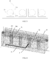
- the filter 1 may include more than three resonators 11, and the near-end rejection structure 14 is located between nonadjacent resonant cavities. As shown in FIG. 1 , the filter 1 includes four resonators, successively marked as cavity 1, cavity 2, cavity 3, and cavity 4 from left to right. The two ends of the near-end rejection structure 14 are respectively located near the cavity 1 and cavity 3. Optionally, the near-end rejection structure 14 may be located between the cavity 1 and cavity 4, or between the cavity 2 and cavity 4.
- the near-end rejection structure 14 located between nonadjacent resonant cavities forms a cross-coupling structure, that is, when signals pass through resonant cavities through different signal paths, phases of different signal paths are canceled, so as to form a transmission zero.
- a signal path of cavity 1-cavity 2-cavity 3 may be considered as a positive phase path, and a signal path of cavity 1-cavity 3 is considered as a negative phase path. Phases of the two paths are canceled, and a transmission zero is formed at the near-end rejection structure 14. The zero is corresponding to the frequency of the signal that the filter is to filter out.
- a near-end rejection structure is disposed inside the dielectric filter and near a lower surface of the dielectric filter, so as to implement an inductive transmission zero function, and reject a radio frequency signal on a high-frequency end out of a passband of the filter, thereby achieving good near-end rejection performance.
- FIG. 2 and FIG. 3 are a front view and a top view of another transverse electromagnetic mode dielectric filter according to an embodiment of the present invention.
- a transverse electromagnetic mode dielectric filter 2 (“filter 2" for short below) includes a resonator 21, a dielectric body 22, a metal housing 23, and a near-end rejection structure 24.
- the metal housing 23 is fastened above the dielectric body 22, and there is a gap between the metal housing 23 and the dielectric body 22.
- the resonator 21 includes a resonant plate 211 and a resonant hole 212.
- the near-end rejection structure 24 is located at an area near a top surface of the dielectric body 22.
- the area is an electric field area inside the dielectric body 22, and the electric field area refers to an area that is inside the dielectric body and that has a stronger electric field than that of another location.
- a specific shape, location, and size of the near-end rejection structure 24 may be determined according to a coupling coefficient of the filter. For a specific determining manner, reference may be made to the description in the embodiment shown in FIG. 1 . This is not described herein.
- the near-end rejection structure 24 plays a capacitive transmission zero role, and can improve a rejection capability on a low-frequency end out of a passband of the filter, that is, can reject a signal on the low-frequency end out of the passband of the filter.
- a transverse electromagnetic mode dielectric filter whose specification is 90*44*20 (mm, millimeter) is used as an example.
- a near-end rejection structure is disposed inside a dielectric body of the filter to serve as a capacitive zero.
- the structure is a metalized through hole whose specific size is as follows: A length is 23 mm, a width is 1 mm, a distance away from a resonant hole is 3 mm, and a distance away from a top surface of the dielectric body, that is, a resonant plate, is 3 mm.
- a passband of the filter is 1805 MHz to 1865 MHz, that is, a radio frequency signal whose frequency is beyond this frequency band can be effectively filtered out.
- a near-end rejection structure is disposed inside the dielectric filter and near a top surface of a dielectric body, so as to implement a capacitive transmission zero function, and reject a radio frequency signal on a low-frequency end out of a passband of the filter, thereby achieving good near-end rejection performance.
- FIG. 4 is a schematic diagram of another transverse electromagnetic mode dielectric filter according to an embodiment of the present invention.
- a transverse electromagnetic mode dielectric filter 3 (“filter 3" for short below) includes a resonator 31, a dielectric body 32, a metal housing 33, and a near-end rejection structure 34.
- the metal housing 33 is fastened above the dielectric body 32, there is a gap between the metal housing 33 and the dielectric body 32, and the resonator 31 includes a resonant plate 301 and a resonant hole 302.
- a wavelength and a frequency of an electromagnetic wave waveform are in a one-to-one correspondence relationship.
- a height, a length, and a distance away from the resonant hole 302 that are of the near-end rejection structure 34 may be determined according to the electrical wavelength.
- a size of the near-end rejection structure 34 may be determined by using filter emulation software, or may be determined according to an experiment or experience. This is not particularly limited in this embodiment of the present invention.
- the near-end rejection structure 34 may be a strip structure with a bending angle, or may be a strip or tube structure with a radian in another embodiment.
- any other parts of the near-end rejection structure 34 may also be contacted to the lower surface of the dielectric body 32.
- the near-end rejection structure 34 may play a zero cavity role, and may improve a rejection capability on a high-frequency end or a low-frequency end out of a passband of the filter, that is, may reject a signal on the high-frequency end or the low-frequency end out of the passband of the filter.
- the electrical wavelength corresponding to the near-end rejection structure 34 may be changed, so as to control the frequency of the signal that the filter is to filter out.
- the length of the near-end rejection structure 34 is inversely proportional to the signal frequency.
- a longer near-end rejection structure 34 indicates a lower corresponding signal frequency, and the filter 3 may be configured to filter out a signal on a low-frequency end.
- a shorter near-end rejection structure 34 indicates a higher corresponding signal frequency, and the filter 3 may be configured to filter out a signal on a high-frequency end.
- This embodiment of the present invention further provides a radio frequency module.
- the radio frequency module includes any transverse electromagnetic mode dielectric filter described in the foregoing embodiments.
- the radio frequency module may be a repeater, a remote radio unit (RRU, remote radio unit), a radio frequency unit (RFU, radio frequency unit), or another device. This is not particularly limited in this embodiment of the present invention.
- a zero cavity function can be implemented by disposing a near-end rejection structure inside a dielectric body; and by using the structure, a signal on a high-frequency end or a low-frequency end out of a passband of the filter can be rejected, and near-end rejection performance of the filter can be improved, thereby improving a filtering effect.
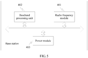
- FIG. 5 is an example diagram of a base station according to an embodiment of the present invention.
- the base station may include a radio frequency module, and the radio frequency module includes the transverse electromagnetic mode dielectric filter shown in any embodiment in FIG. 1 to FIG. 4 .
- the base station may further include a baseband processing unit (BBU, base band unit) 402, a power module 403, and the like. All modules or units may be connected by using a communications bus.
- BBU baseband processing unit
- All modules or units may be connected by using a communications bus.
- the base station may be a small cell (small cell) device, such as an indoor small cell product.
- small cell small cell
- the radio frequency module or the base station provided in this embodiment of the present invention uses a transverse electromagnetic mode dielectric filter with good near-end rejection performance, and therefore has low costs and a small size.
- An embodiment of the present invention further provides a method for producing any transverse electromagnetic mode dielectric filter ("filter” for short below) according to FIG. 1 to FIG. 4 .
- the method includes: preparing two layers or multiple layers of dielectric blank raw materials; after a through hole or a blind hole is provided on the two layers or multiple layers of dielectric raw materials, separately sintering each layer of dielectric raw material; preparing a metalized structure and a punching on each layer of sintered dielectric; then forming a filter entirety by means of bonding; and forming the transverse electromagnetic mode dielectric filter provided in this embodiment of the present invention after metallization of a printed pattern of the filter is completed.
- the method may be: preparing two layers or multiple layers of dielectric blank raw materials; obtaining a required metal structure, that is, a transmission zero or zero cavity structure in the present invention, by means of opening a hole, printing a circuit, and the like on each layer of dielectric raw material; then stacking prepared layers of dielectric raw materials together for sintering; and finally forming the transverse electromagnetic mode dielectric filter provided in this embodiment of the present invention after metallization of a printed pattern of the dielectric filter is completed.
Description
- Embodiments of the present invention relate to the field of communications technologies, and in particular, to a transverse electromagnetic mode dielectric filter, a radio frequency module, and a base station.
- With development of wireless communications technologies, a wireless communications device increasingly strives for miniaturization and a low insertion loss. Compared with a conventional metal cavity filter, a dielectric filter has an advantage such as a small size, a low insertion loss, high bearing power, and low costs. A transverse electromagnetic mode (TEM, transverse electromagnetic mode) dielectric filter is an important dielectric filter type, and may be applied to a device such as a wireless base station, a radio frequency terminal, or a radio frequency or microwave transceiver component.
- However, a transverse electromagnetic mode dielectric filter provided in the prior art has poor near-end rejection performance, and therefore, cannot be applied to a location, such as a radio frequency front-end or a microwave antenna feeder front-end, that has a relatively high requirement on filter performance. Consequently, an application scenario is limited. From
US 2012/0326806 A1 RF monoblock filters comprising metallized filter structures on a dielectric lid are known. FromWO2007/142786 A1 (CTS Corp [US]) ceramic monoblock filters comprising cross-coupling signal means at a top surface of a dielectric body are known. FromUS 5,537,085 ceramic filters comprising a magnetic coupling on a side surface of a dielectric body are known. - Embodiments of the present invention provide a transverse electromagnetic mode dielectric filter that has good near-end rejection performance; and the embodiments of the present invention further provide a radio frequency module and a base station.
- The present invention provides a transverse electromagnetic mode dielectric filter according to the subject-matter of the present claims.
- According to technical solutions provided in the embodiments of the present invention, a near-end rejection structure is disposed inside a transverse electromagnetic mode dielectric filter. By flexibly designing a shape, a location, and a size of the near-end rejection structure, a transmission zero or zero cavity function is implemented, and a radio frequency signal on a high-frequency end or a low-frequency end out of a passband of the filter is rejected. The transverse electromagnetic mode dielectric filter provided in the embodiments of the present invention has good near-end rejection performance, and may be widely applied to a radio frequency module and a base station.
- To describe the technical solutions in the embodiments of the present invention more clearly, the following briefly describes the accompanying drawings required for describing the embodiments. Apparently, the accompanying drawings in the following description show merely some embodiments of the present invention, and persons of ordinary skill in the art may still derive other drawings from these accompanying drawings without creative efforts.
-
FIG. 1 is a schematic structural diagram of a transverse electromagnetic mode dielectric filter according to an embodiment of the present invention; -
FIG. 2 is a front view of another transverse electromagnetic mode dielectric filter according to an embodiment of the present invention; -
FIG. 3 is a top view of another transverse electromagnetic mode dielectric filter according to an embodiment of the present invention; -
FIG. 4 is a schematic structural diagram of another transverse electromagnetic mode dielectric filter according to an embodiment of the present invention; and -
FIG. 5 is a schematic structural diagram of a base station according to an embodiment of the present invention. - To make the objectives, technical solutions, and advantages of the present invention clearer, the following further describes implementations of the present invention in detail with reference to the accompanying drawings.
- A filter is a necessary component in a device such as a base station or a radio frequency terminal. With an advantage in costs, size, and the like, a dielectric filter may be applied at a location such as a receive link of the base station, and is configured to perform filtering on a radio frequency signal. A transverse electromagnetic mode dielectric filter is a widely-used dielectric filter.
- However, a radio frequency performance indicator of the transverse electromagnetic mode dielectric filter is relatively poor, and cannot be used at a location, such as a front-end of a radio frequency module, that is, a location between a transmit antenna and a power amplifier, that has a relatively high requirement on the performance of the filter. The radio frequency performance indicator of the filter includes multiple indicators such as an insertion loss, rejection, and inter-modulation. Therefore, an application scenario of the transverse electromagnetic mode dielectric filter is greatly limited.
- A main reason causing the relatively poor radio frequency performance indicator of the transverse electromagnetic mode dielectric filter is that near-end rejection performance of this type of filter is poor. Near-end rejection is also referred to as sideband rejection or near band rejection (near band rejection), and means performing strong rejection on a signal on a high-frequency end or a low-frequency end near an outside area of a passband of the filter, so as to ensure a filtering effect. Currently, a design method for cross-coupling or resonance of the transverse electromagnetic mode dielectric filter is inflexible, a transmission zero or zero cavity structure cannot be formed effectively, and therefore, the filter does not have good near-end rejection performance.
-
FIG. 1 is a schematic diagram of a transverse electromagnetic mode dielectric filter according to an embodiment of the present invention. - As shown in
FIG. 1 , a transverse electromagnetic mode dielectric filter 1 ("filter 1" for short below) includes aresonator 11, adielectric body 12, and ametal housing 13. Themetal housing 13 is fastened above thedielectric body 12, and there is a gap between themetal housing 13 and thedielectric body 12. - An outer surface of the
dielectric body 12 is covered with a conductive material. Optionally, a metal coating, such as a silver coating, may be used. - The gap between the
metal housing 13 and thedielectric body 12 is filled with air. - The
resonator 11 includes aresonant plate 101 and aresonant hole 102, and theresonant plate 101 is disposed on a top surface of thedielectric body 12. - Optionally, the
resonant plate 101 may be a thin metal piece disposed on the top surface of thedielectric body 12, or may be a metal coating printed on the top surface of thedielectric body 12. - Optionally, a shape of the
resonant plate 101 is not limited. For example, the shape may be a regular figure such as a rectangle or a circle, or may be modified on the basis of the regular figure according to specifications and a performance requirement of the filter, for example, a specific area is cut off to form an irregular figure. This is not particularly limited in this embodiment of the present invention. - The
resonant hole 102 is a hollow cylindrical structure with openings on upper and lower ends, an upper opening of theresonant hole 102 is provided on theresonant plate 101, a lower opening of theresonant hole 102 is provided on a lower surface of thedielectric body 12, and an inner surface of theresonant hole 102 is covered with a conductive material. - Optionally, the conductive material covering the inner surface of the
resonant hole 102 may be a metal coating, such as a silver coating. - Optionally, the
resonant hole 102 and theresonant plate 101 may be integrally formed, or may be separately made and then formed by means of connection. - The filter 1 further includes a near-
end rejection structure 14. The near-end rejection structure 14 is inside thedielectric body 12, and a shape, a location, and a size of the near-end rejection structure 14 are determined by a frequency of a signal that the filter is to filter out. - As shown in
FIG. 1 , two ends of the near-end rejection structure 14 are in contact with the lower surface of thedielectric body 12, and a remaining part of the near-end rejection structure 14 is within a magnetic field area inside thedielectric body 12. The magnetic field area refers to an area that is inside the dielectric body and that has a stronger magnetic field than that of another location. - A strong magnetic field area inside the
dielectric body 12 is an area near the lower surface of thedielectric body 12. - Optionally, a height, a length, and a distance away from the resonant hole that are of the near-
end rejection structure 14 may be determined according to a coupling coefficient (coupling coefficient) of the filter, and the coupling coefficient is corresponding to the frequency of the signal that the filter is to filter out. - The coupling coefficient is an important parameter during filter design. When the coupling coefficient is determined, a physical structure of the filter may be designed according to the coupling coefficient, and a corresponding performance indicator may be achieved. Generally, the coupling coefficient may be obtained by solving a coupling matrix (coupling matrix). The coupling matrix may be used to indicate a coupling energy relationship between resonant cavities, and the coupling coefficient is included in the coupling matrix.
- Optionally, the coupling matrix may be obtained by means of calculation by using filter emulation software, or may be determined according to an experimental or empirical value. This is not particularly limited in this embodiment of the present invention.
- Optionally, the near-
end rejection structure 14 may be any one of a metalized through hole, a metalized strip line, a physical metal structure, a metalized conductor, or a thin metal piece. - Optionally, the near-
end rejection structure 14 may be a strip structure with a specific radian. Specifically, the radian may be determined by means of debugging according to the performance requirement of the filter. This is not particularly limited in this embodiment of the present invention. - Optionally, in another embodiment of the present invention, in addition to the two ends, any other part of the near-
end rejection structure 14 may also be in contact with the lower surface of thedielectric body 12, to play a grounding role. - In the embodiment shown in
FIG. 1 , the near-end rejection structure 14 plays an inductive transmission zero role, and can improve a rejection capability on a high-frequency end out of a passband of the filter, that is, can reject a signal on the high-frequency end out of the passband of the filter. It may be understood that the near-end rejection structure 14 may be designed for only one specific signal frequency, and when the filter has strong rejection over a specific frequency, the filter has good rejection over a frequency band neighboring to the frequency. - Optionally, the filter 1 may include more than three
resonators 11, and the near-end rejection structure 14 is located between nonadjacent resonant cavities. As shown inFIG. 1 , the filter 1 includes four resonators, successively marked as cavity 1, cavity 2,cavity 3, and cavity 4 from left to right. The two ends of the near-end rejection structure 14 are respectively located near the cavity 1 andcavity 3. Optionally, the near-end rejection structure 14 may be located between the cavity 1 and cavity 4, or between the cavity 2 and cavity 4. - The near-
end rejection structure 14 located between nonadjacent resonant cavities forms a cross-coupling structure, that is, when signals pass through resonant cavities through different signal paths, phases of different signal paths are canceled, so as to form a transmission zero. For example, a signal path of cavity 1-cavity 2-cavity 3 may be considered as a positive phase path, and a signal path of cavity 1-cavity 3 is considered as a negative phase path. Phases of the two paths are canceled, and a transmission zero is formed at the near-end rejection structure 14. The zero is corresponding to the frequency of the signal that the filter is to filter out. - According to the transverse electromagnetic mode dielectric filter provided in this embodiment of the present invention, a near-end rejection structure is disposed inside the dielectric filter and near a lower surface of the dielectric filter, so as to implement an inductive transmission zero function, and reject a radio frequency signal on a high-frequency end out of a passband of the filter, thereby achieving good near-end rejection performance.
-
FIG. 2 andFIG. 3 are a front view and a top view of another transverse electromagnetic mode dielectric filter according to an embodiment of the present invention. - As shown in
FIG. 2 , a transverse electromagnetic mode dielectric filter 2 ("filter 2" for short below) includes aresonator 21, adielectric body 22, ametal housing 23, and a near-end rejection structure 24. Themetal housing 23 is fastened above thedielectric body 22, and there is a gap between themetal housing 23 and thedielectric body 22. As shown inFIG. 3 , theresonator 21 includes aresonant plate 211 and aresonant hole 212. - Overall structures of the filter 2 and the filter 1 provided in the embodiment shown in
FIG. 1 are similar, and what is different from the embodiment shown inFIG. 1 is that the near-end rejection structure 24 is located at an area near a top surface of thedielectric body 22. The area is an electric field area inside thedielectric body 22, and the electric field area refers to an area that is inside the dielectric body and that has a stronger electric field than that of another location. A specific shape, location, and size of the near-end rejection structure 24 may be determined according to a coupling coefficient of the filter. For a specific determining manner, reference may be made to the description in the embodiment shown inFIG. 1 . This is not described herein. - In the embodiments shown in
FIG. 2 andFIG. 3 , the near-end rejection structure 24 plays a capacitive transmission zero role, and can improve a rejection capability on a low-frequency end out of a passband of the filter, that is, can reject a signal on the low-frequency end out of the passband of the filter. - It may be understood that for detailed description of another component in the filter 2, reference may be made to the content in the embodiment shown in
FIG. 1 . This is not described herein. - A transverse electromagnetic mode dielectric filter whose specification is 90*44*20 (mm, millimeter) is used as an example. A near-end rejection structure is disposed inside a dielectric body of the filter to serve as a capacitive zero. The structure is a metalized through hole whose specific size is as follows: A length is 23 mm, a width is 1 mm, a distance away from a resonant hole is 3 mm, and a distance away from a top surface of the dielectric body, that is, a resonant plate, is 3 mm. A passband of the filter is 1805 MHz to 1865 MHz, that is, a radio frequency signal whose frequency is beyond this frequency band can be effectively filtered out.
- According to the transverse electromagnetic mode dielectric filter provided in this embodiment of the present invention, a near-end rejection structure is disposed inside the dielectric filter and near a top surface of a dielectric body, so as to implement a capacitive transmission zero function, and reject a radio frequency signal on a low-frequency end out of a passband of the filter, thereby achieving good near-end rejection performance.
-
FIG. 4 is a schematic diagram of another transverse electromagnetic mode dielectric filter according to an embodiment of the present invention. - As shown in
FIG. 4 , a transverse electromagnetic mode dielectric filter 3 ("filter 3" for short below) includes aresonator 31, adielectric body 32, ametal housing 33, and a near-end rejection structure 34. Themetal housing 33 is fastened above thedielectric body 32, there is a gap between themetal housing 33 and thedielectric body 32, and theresonator 31 includes aresonant plate 301 and aresonant hole 302. - Overall structures of the
filter 3 and the transverse electromagnetic mode dielectric filter provided in the embodiment inFIG. 1 or FIG. 2 andFIG. 3 are similar, and what is different from the filter shown inFIG. 1 or FIG. 2 is that a shape, a location, and a size of the near-end rejection structure 34 are determined by an electrical wavelength corresponding to a frequency of a signal that the filter is to filter out. The electrical wavelength is an electromagnetic wave wavelength. - Specifically, the electrical wavelength may be calculated according to a formula: c=λ*f, where f is a signal frequency, λ is an electrical wavelength, and c is a constant.
- It can be learned that a wavelength and a frequency of an electromagnetic wave waveform are in a one-to-one correspondence relationship. A height, a length, and a distance away from the
resonant hole 302 that are of the near-end rejection structure 34 may be determined according to the electrical wavelength. Specifically, a size of the near-end rejection structure 34 may be determined by using filter emulation software, or may be determined according to an experiment or experience. This is not particularly limited in this embodiment of the present invention. - Optionally, as shown in
FIG. 4 , the near-end rejection structure 34 may be a strip structure with a bending angle, or may be a strip or tube structure with a radian in another embodiment. - As shown in
FIG. 4 , two ends of the near-end rejection structure 34 are contacted to a lower surface of thedielectric body 32. Optionally, in another embodiment, in addition to the two ends, any other parts of the near-end rejection structure 34 may also be contacted to the lower surface of thedielectric body 32. - In the embodiment shown in
FIG. 4 , the near-end rejection structure 34 may play a zero cavity role, and may improve a rejection capability on a high-frequency end or a low-frequency end out of a passband of the filter, that is, may reject a signal on the high-frequency end or the low-frequency end out of the passband of the filter. - Optionally, by changing a structure of the near-
end rejection structure 34, such as changing a length, the electrical wavelength corresponding to the near-end rejection structure 34 may be changed, so as to control the frequency of the signal that the filter is to filter out. Specifically, the length of the near-end rejection structure 34 is inversely proportional to the signal frequency. A longer near-end rejection structure 34 indicates a lower corresponding signal frequency, and thefilter 3 may be configured to filter out a signal on a low-frequency end. A shorter near-end rejection structure 34 indicates a higher corresponding signal frequency, and thefilter 3 may be configured to filter out a signal on a high-frequency end. - It may be understood that for detailed description of another component in the
filter 3, reference may be made to the content in the embodiment shown inFIG. 1 or FIG. 2 andFIG. 3 . This is not described herein. - This embodiment of the present invention further provides a radio frequency module. The radio frequency module includes any transverse electromagnetic mode dielectric filter described in the foregoing embodiments.
- Optionally, the radio frequency module may be a repeater, a remote radio unit (RRU, remote radio unit), a radio frequency unit (RFU, radio frequency unit), or another device. This is not particularly limited in this embodiment of the present invention.
- According to the transverse electromagnetic mode dielectric filter or the radio frequency module provided in this embodiment of the present invention, when a size of the filter is not increased, a zero cavity function can be implemented by disposing a near-end rejection structure inside a dielectric body; and by using the structure, a signal on a high-frequency end or a low-frequency end out of a passband of the filter can be rejected, and near-end rejection performance of the filter can be improved, thereby improving a filtering effect.
-
FIG. 5 is an example diagram of a base station according to an embodiment of the present invention. The base station may include a radio frequency module, and the radio frequency module includes the transverse electromagnetic mode dielectric filter shown in any embodiment inFIG. 1 to FIG. 4 . - The base station may further include a baseband processing unit (BBU, base band unit) 402, a
power module 403, and the like. All modules or units may be connected by using a communications bus. - Optionally, the base station may be a small cell (small cell) device, such as an indoor small cell product.
- The radio frequency module or the base station provided in this embodiment of the present invention uses a transverse electromagnetic mode dielectric filter with good near-end rejection performance, and therefore has low costs and a small size.
- An embodiment of the present invention further provides a method for producing any transverse electromagnetic mode dielectric filter ("filter" for short below) according to
FIG. 1 to FIG. 4 . - The method includes: preparing two layers or multiple layers of dielectric blank raw materials; after a through hole or a blind hole is provided on the two layers or multiple layers of dielectric raw materials, separately sintering each layer of dielectric raw material; preparing a metalized structure and a punching on each layer of sintered dielectric; then forming a filter entirety by means of bonding; and forming the transverse electromagnetic mode dielectric filter provided in this embodiment of the present invention after metallization of a printed pattern of the filter is completed.
- In another embodiment of the present invention, the method may be: preparing two layers or multiple layers of dielectric blank raw materials; obtaining a required metal structure, that is, a transmission zero or zero cavity structure in the present invention, by means of opening a hole, printing a circuit, and the like on each layer of dielectric raw material; then stacking prepared layers of dielectric raw materials together for sintering; and finally forming the transverse electromagnetic mode dielectric filter provided in this embodiment of the present invention after metallization of a printed pattern of the dielectric filter is completed.
Claims (5)
- A transverse electromagnetic mode dielectric filter (1, 2, 3), comprising:
a resonator (11, 21, 31), a dielectric body (12, 22, 32), and a metal housing (13, 23, 33), wherein- an outer surface of the dielectric body (12, 22, 32) is covered with a conductive material, the metal housing (13, 23, 33) is fastened above the dielectric body (12, 22, 32), and there is a gap between the metal housing (13, 23, 33) and the dielectric body (12, 22, 32);- the resonator (11, 21, 31) comprises a resonant plate (101, 201, 301) and a resonant hole (102, 202, 302), wherein the resonant plate (102, 202, 302) is disposed on a top surface of the dielectric body (12, 22, 32), the resonant hole (102, 202, 302) is a hollow cylindrical structure with openings on upper and lower ends, an upper opening of the resonant hole (102, 202, 302) is provided on the resonant plate (101, 201, 301), a lower opening of the resonant hole is provided on a lower surface of the dielectric body (12, 22, 32), an inner surface of the resonant hole (102, 202, 302) is covered with a conductive material, and the resonant plate (101, 201, 301) is of a metal material; and- the filter (1, 2, 3) further comprises a near-end rejection structure (14, 24, 34), wherein the near-end rejection structure (14, 24, 34) is inside the dielectric body (12, 22, 32), and a shape, a location, and a size of the near-end rejection structure (14, 24, 34) are configured according to a frequency of a signal that the filter (1, 2, 3) is to filter out;- the near-end rejection structure is a near high-frequency end-rejection structure or a near low-frequency end-rejection structure;- the near-end rejection structure (14, 24, 34) has at least two ends in contact with the lower surface of the dielectric body (12, 22, 32), and a remaining part of the near-end rejection structure (14, 24, 34) is within a magnetic field area inside the dielectric body
or
the near-end rejection structure (14, 24, 34) is within an electric field area inside the dielectric body (12, 22, 32); and- the near-end rejection structure (14, 24, 34) is any one of a metalized through hole, a metalized strip line, a physical metal structure, a metalized conductor, or a thin metal piece. - The filter (1, 2, 3) according to claim 1, wherein a height, a length, and a distance away from the resonant hole (102, 202, 302) that are of the near-end rejection structure (14, 24, 34) are configured according to a coupling coefficient of the filter (1, 2, 3), wherein the coupling coefficient is corresponding to the frequency of the signal that the filter (1, 2, 3) is to filter out.
- The filter (1, 2, 3) according to claim 1, wherein a height, a length, and a distance away from the resonant hole (102, 202, 302) that are of the near-end rejection structure (14, 24, 34) are configured according to an electrical wavelength corresponding to the frequency of the signal that the filter (1, 2, 3) is to filter out.
- A radio frequency module, comprising the transverse electromagnetic mode dielectric filter according to any one of claims 1 to 3.
- A base station, comprising the radio frequency module according to claim 4.
Applications Claiming Priority (2)
| Application Number | Priority Date | Filing Date | Title |
|---|---|---|---|
| CN201410743332.9A CN104466315B (en) | 2014-12-08 | 2014-12-08 | Transverse electromagnetic mode dielectric filter, radio-frequency module and base station |
| PCT/CN2015/085087 WO2016090925A1 (en) | 2014-12-08 | 2015-07-24 | Transverse electromagnetic mode dielectric filter, radio frequency module and base station |
Publications (3)
| Publication Number | Publication Date |
|---|---|
| EP3217468A1 EP3217468A1 (en) | 2017-09-13 |
| EP3217468A4 EP3217468A4 (en) | 2017-11-29 |
| EP3217468B1 true EP3217468B1 (en) | 2021-01-06 |
Family
ID=52911977
Family Applications (1)
| Application Number | Title | Priority Date | Filing Date |
|---|---|---|---|
| EP15867903.5A Active EP3217468B1 (en) | 2014-12-08 | 2015-07-24 | Transverse electromagnetic mode dielectric filter, radio frequency module and base station |
Country Status (5)
| Country | Link |
|---|---|
| EP (1) | EP3217468B1 (en) |
| JP (1) | JP2017537581A (en) |
| CN (1) | CN104466315B (en) |
| CA (1) | CA2970054C (en) |
| WO (1) | WO2016090925A1 (en) |
Families Citing this family (6)
| Publication number | Priority date | Publication date | Assignee | Title |
|---|---|---|---|---|
| CN104466315B (en) * | 2014-12-08 | 2017-11-24 | 上海华为技术有限公司 | Transverse electromagnetic mode dielectric filter, radio-frequency module and base station |
| CN109219904A (en) * | 2016-12-29 | 2019-01-15 | 深圳市大富科技股份有限公司 | A kind of TEM mode filter and communication equipment |
| CN107359394B (en) * | 2017-08-15 | 2020-09-11 | 罗森伯格技术有限公司 | Adjustable electromagnetic hybrid coupling filter |
| CN108493538B (en) * | 2018-04-11 | 2024-04-16 | 广东通宇通讯股份有限公司 | Cavity filter capable of adjusting coupling strength |
| WO2023159482A1 (en) * | 2022-02-25 | 2023-08-31 | Telefonaktiebolaget Lm Ericsson (Publ) | A communication device |
| CN115411476B (en) * | 2022-08-19 | 2023-09-05 | 北京遥测技术研究所 | Miniature all-metal micro-coaxial microwave filter chip |
Citations (2)
| Publication number | Priority date | Publication date | Assignee | Title |
|---|---|---|---|---|
| US4692726A (en) * | 1986-07-25 | 1987-09-08 | Motorola, Inc. | Multiple resonator dielectric filter |
| WO2008051572A1 (en) * | 2006-10-27 | 2008-05-02 | Cts Corporation | Monoblock rf resonator/filter |
Family Cites Families (18)
| Publication number | Priority date | Publication date | Assignee | Title |
|---|---|---|---|---|
| US5537085A (en) * | 1994-04-28 | 1996-07-16 | Motorola, Inc. | Interdigital ceramic filter with transmission zero |
| KR970008855A (en) * | 1996-11-08 | 1997-02-24 | 김덕용 | Dielectric resonator filter |
| US5850168A (en) * | 1997-04-18 | 1998-12-15 | Motorola Inc. | Ceramic transverse-electromagnetic-mode filter having a waveguide cavity mode frequency shifting void and method of tuning same |
| TW409458B (en) * | 1998-11-03 | 2000-10-21 | Samsung Electro Mech | Dielectric filter |
| KR100342442B1 (en) * | 1999-11-03 | 2002-06-28 | 성규제 | Microwave Bandpass Filter Using TEM mode Ceramic Coaxial Resonators with Microstrip Pattern Coupling |
| JP3883902B2 (en) * | 2002-04-25 | 2007-02-21 | 三洋電機株式会社 | Dielectric filter |
| JP4494931B2 (en) * | 2004-10-19 | 2010-06-30 | 日本特殊陶業株式会社 | Dielectric porcelain composition and electronic component using the same |
| JP2007028141A (en) * | 2005-07-15 | 2007-02-01 | Toko Inc | Dielectric filter |
| WO2007142786A1 (en) * | 2006-05-31 | 2007-12-13 | Cts Corporation | Ceramic monoblock filter with inductive direct-coupling and quadruplet cross-coupling |
| CN101340014B (en) * | 2008-08-01 | 2012-04-04 | 苏州艾福电子通讯有限公司 | Ceramic dielectric filter and duplexer having slots |
| US9030276B2 (en) * | 2008-12-09 | 2015-05-12 | Cts Corporation | RF monoblock filter with a dielectric core and with a second filter disposed in a side surface of the dielectric core |
| CN103050752B (en) * | 2009-08-11 | 2016-06-01 | 京信通信系统(中国)有限公司 | Cavity medium filter and Out-of-band rejection method thereof |
| JP5569686B2 (en) * | 2010-07-29 | 2014-08-13 | 宇部興産株式会社 | Dielectric resonant component and mounting structure using the same |
| CN102760923B (en) * | 2012-08-02 | 2015-04-29 | 深圳市国人射频通信有限公司 | Medium filter |
| CN202855879U (en) * | 2012-09-18 | 2013-04-03 | 武汉凡谷电子技术股份有限公司 | Adjustable electric coupling structure between TEM die metal chamber and TM die medium chamber in filter |
| CN203260696U (en) * | 2012-12-03 | 2013-10-30 | 武汉凡谷电子技术股份有限公司 | TM mode dielectric filter |
| CN103928731A (en) * | 2014-04-30 | 2014-07-16 | 华为技术有限公司 | TEM mode dielectric filter and manufacturing method |
| CN104466315B (en) * | 2014-12-08 | 2017-11-24 | 上海华为技术有限公司 | Transverse electromagnetic mode dielectric filter, radio-frequency module and base station |
-
2014
- 2014-12-08 CN CN201410743332.9A patent/CN104466315B/en active Active
-
2015
- 2015-07-24 JP JP2017548510A patent/JP2017537581A/en active Pending
- 2015-07-24 CA CA2970054A patent/CA2970054C/en active Active
- 2015-07-24 EP EP15867903.5A patent/EP3217468B1/en active Active
- 2015-07-24 WO PCT/CN2015/085087 patent/WO2016090925A1/en active Application Filing
Patent Citations (2)
| Publication number | Priority date | Publication date | Assignee | Title |
|---|---|---|---|---|
| US4692726A (en) * | 1986-07-25 | 1987-09-08 | Motorola, Inc. | Multiple resonator dielectric filter |
| WO2008051572A1 (en) * | 2006-10-27 | 2008-05-02 | Cts Corporation | Monoblock rf resonator/filter |
Also Published As
| Publication number | Publication date |
|---|---|
| CA2970054A1 (en) | 2016-06-16 |
| CN104466315B (en) | 2017-11-24 |
| JP2017537581A (en) | 2017-12-14 |
| CA2970054C (en) | 2019-04-23 |
| WO2016090925A1 (en) | 2016-06-16 |
| EP3217468A1 (en) | 2017-09-13 |
| EP3217468A4 (en) | 2017-11-29 |
| CN104466315A (en) | 2015-03-25 |
Similar Documents
| Publication | Publication Date | Title |
|---|---|---|
| EP3217468B1 (en) | Transverse electromagnetic mode dielectric filter, radio frequency module and base station | |
| US9893399B2 (en) | Waveguide filter | |
| CN107681275B (en) | Antenna and electronic device | |
| EP3370300B1 (en) | Dielectric resonator, dielectric filter, and fabrication method | |
| US9748641B2 (en) | Antenna device and method for designing same | |
| WO2014157947A1 (en) | Planar antenna apparatus and method | |
| CN103151584A (en) | Cavity filter, radio-frequency zooming-out equipment, signal receiving-transmitting device and tower top amplifier | |
| CN107516753A (en) | A kind of wave filter based on the incomplete mould of substrate integration wave-guide | |
| CN107134614B (en) | A kind of multi-layer ceramics microwave band-pass filter | |
| WO2021081769A1 (en) | Cavity filter and electromagnetic wave device | |
| CN113328219B (en) | Dielectric filter and communication apparatus | |
| CN204991909U (en) | Miniaturized radio frequency identification band pass filter | |
| CN104332683B (en) | A kind of dual-passband hexagon wave filter for being applied to PCS & WiMAX frequency ranges | |
| EP3159966B1 (en) | Antenna device and terminal | |
| CN204067572U (en) | Groove is utilized to suppress the printing type monopole antenna of frequency range | |
| EP2747191B1 (en) | Filter | |
| EP3883050B1 (en) | Dielectric filter, duplexer, and communication device | |
| CN210092347U (en) | Filtering antenna for wireless communication system | |
| JP2011091781A (en) | Composite filter and radio communication module employing the same and radio communication device | |
| CN102637928B (en) | Dielectric filter | |
| CN210693919U (en) | NB-IoT communication module with strong anti-interference performance | |
| KR100332878B1 (en) | Duplexer dielectric filter | |
| CN105322254A (en) | Direct-feed planar dual-mode ring band-pass filter with adjustable bandwidth | |
| CN117791068A (en) | Dual-mode dual-passband filter with independently adjustable bandwidth and frequency and modulation method | |
| CN117941171A (en) | Integrated low pass band pass filter unit formed of metal plates coated with dielectric material |
Legal Events
| Date | Code | Title | Description |
|---|---|---|---|
| STAA | Information on the status of an ep patent application or granted ep patent |
Free format text: STATUS: THE INTERNATIONAL PUBLICATION HAS BEEN MADE |
|
| PUAI | Public reference made under article 153(3) epc to a published international application that has entered the european phase |
Free format text: ORIGINAL CODE: 0009012 |
|
| STAA | Information on the status of an ep patent application or granted ep patent |
Free format text: STATUS: REQUEST FOR EXAMINATION WAS MADE |
|
| 17P | Request for examination filed |
Effective date: 20170608 |
|
| AK | Designated contracting states |
Kind code of ref document: A1 Designated state(s): AL AT BE BG CH CY CZ DE DK EE ES FI FR GB GR HR HU IE IS IT LI LT LU LV MC MK MT NL NO PL PT RO RS SE SI SK SM TR |
|
| AX | Request for extension of the european patent |
Extension state: BA ME |
|
| A4 | Supplementary search report drawn up and despatched |
Effective date: 20171026 |
|
| RIC1 | Information provided on ipc code assigned before grant |
Ipc: H01P 1/205 20060101ALI20171020BHEP Ipc: H01P 1/201 20060101AFI20171020BHEP |
|
| DAV | Request for validation of the european patent (deleted) | ||
| DAX | Request for extension of the european patent (deleted) | ||
| STAA | Information on the status of an ep patent application or granted ep patent |
Free format text: STATUS: EXAMINATION IS IN PROGRESS |
|
| 17Q | First examination report despatched |
Effective date: 20191218 |
|
| GRAP | Despatch of communication of intention to grant a patent |
Free format text: ORIGINAL CODE: EPIDOSNIGR1 |
|
| STAA | Information on the status of an ep patent application or granted ep patent |
Free format text: STATUS: GRANT OF PATENT IS INTENDED |
|
| INTG | Intention to grant announced |
Effective date: 20200728 |
|
| GRAS | Grant fee paid |
Free format text: ORIGINAL CODE: EPIDOSNIGR3 |
|
| GRAA | (expected) grant |
Free format text: ORIGINAL CODE: 0009210 |
|
| STAA | Information on the status of an ep patent application or granted ep patent |
Free format text: STATUS: THE PATENT HAS BEEN GRANTED |
|
| AK | Designated contracting states |
Kind code of ref document: B1 Designated state(s): AL AT BE BG CH CY CZ DE DK EE ES FI FR GB GR HR HU IE IS IT LI LT LU LV MC MK MT NL NO PL PT RO RS SE SI SK SM TR |
|
| REG | Reference to a national code |
Ref country code: GB Ref legal event code: FG4D |
|
| REG | Reference to a national code |
Ref country code: AT Ref legal event code: REF Ref document number: 1353362 Country of ref document: AT Kind code of ref document: T Effective date: 20210115 Ref country code: CH Ref legal event code: EP |
|
| REG | Reference to a national code |
Ref country code: DE Ref legal event code: R096 Ref document number: 602015064596 Country of ref document: DE |
|
| REG | Reference to a national code |
Ref country code: IE Ref legal event code: FG4D |
|
| REG | Reference to a national code |
Ref country code: NL Ref legal event code: MP Effective date: 20210106 |
|
| REG | Reference to a national code |
Ref country code: AT Ref legal event code: MK05 Ref document number: 1353362 Country of ref document: AT Kind code of ref document: T Effective date: 20210106 |
|
| REG | Reference to a national code |
Ref country code: LT Ref legal event code: MG9D |
|
| PG25 | Lapsed in a contracting state [announced via postgrant information from national office to epo] |
Ref country code: NO Free format text: LAPSE BECAUSE OF FAILURE TO SUBMIT A TRANSLATION OF THE DESCRIPTION OR TO PAY THE FEE WITHIN THE PRESCRIBED TIME-LIMIT Effective date: 20210406 Ref country code: PT Free format text: LAPSE BECAUSE OF FAILURE TO SUBMIT A TRANSLATION OF THE DESCRIPTION OR TO PAY THE FEE WITHIN THE PRESCRIBED TIME-LIMIT Effective date: 20210506 Ref country code: GR Free format text: LAPSE BECAUSE OF FAILURE TO SUBMIT A TRANSLATION OF THE DESCRIPTION OR TO PAY THE FEE WITHIN THE PRESCRIBED TIME-LIMIT Effective date: 20210407 Ref country code: HR Free format text: LAPSE BECAUSE OF FAILURE TO SUBMIT A TRANSLATION OF THE DESCRIPTION OR TO PAY THE FEE WITHIN THE PRESCRIBED TIME-LIMIT Effective date: 20210106 Ref country code: FI Free format text: LAPSE BECAUSE OF FAILURE TO SUBMIT A TRANSLATION OF THE DESCRIPTION OR TO PAY THE FEE WITHIN THE PRESCRIBED TIME-LIMIT Effective date: 20210106 Ref country code: LT Free format text: LAPSE BECAUSE OF FAILURE TO SUBMIT A TRANSLATION OF THE DESCRIPTION OR TO PAY THE FEE WITHIN THE PRESCRIBED TIME-LIMIT Effective date: 20210106 Ref country code: BG Free format text: LAPSE BECAUSE OF FAILURE TO SUBMIT A TRANSLATION OF THE DESCRIPTION OR TO PAY THE FEE WITHIN THE PRESCRIBED TIME-LIMIT Effective date: 20210406 |
|
| PG25 | Lapsed in a contracting state [announced via postgrant information from national office to epo] |
Ref country code: SE Free format text: LAPSE BECAUSE OF FAILURE TO SUBMIT A TRANSLATION OF THE DESCRIPTION OR TO PAY THE FEE WITHIN THE PRESCRIBED TIME-LIMIT Effective date: 20210106 Ref country code: AT Free format text: LAPSE BECAUSE OF FAILURE TO SUBMIT A TRANSLATION OF THE DESCRIPTION OR TO PAY THE FEE WITHIN THE PRESCRIBED TIME-LIMIT Effective date: 20210106 Ref country code: PL Free format text: LAPSE BECAUSE OF FAILURE TO SUBMIT A TRANSLATION OF THE DESCRIPTION OR TO PAY THE FEE WITHIN THE PRESCRIBED TIME-LIMIT Effective date: 20210106 Ref country code: LV Free format text: LAPSE BECAUSE OF FAILURE TO SUBMIT A TRANSLATION OF THE DESCRIPTION OR TO PAY THE FEE WITHIN THE PRESCRIBED TIME-LIMIT Effective date: 20210106 Ref country code: RS Free format text: LAPSE BECAUSE OF FAILURE TO SUBMIT A TRANSLATION OF THE DESCRIPTION OR TO PAY THE FEE WITHIN THE PRESCRIBED TIME-LIMIT Effective date: 20210106 |
|
| PG25 | Lapsed in a contracting state [announced via postgrant information from national office to epo] |
Ref country code: IS Free format text: LAPSE BECAUSE OF FAILURE TO SUBMIT A TRANSLATION OF THE DESCRIPTION OR TO PAY THE FEE WITHIN THE PRESCRIBED TIME-LIMIT Effective date: 20210506 |
|
| REG | Reference to a national code |
Ref country code: DE Ref legal event code: R097 Ref document number: 602015064596 Country of ref document: DE |
|
| PG25 | Lapsed in a contracting state [announced via postgrant information from national office to epo] |
Ref country code: SM Free format text: LAPSE BECAUSE OF FAILURE TO SUBMIT A TRANSLATION OF THE DESCRIPTION OR TO PAY THE FEE WITHIN THE PRESCRIBED TIME-LIMIT Effective date: 20210106 Ref country code: CZ Free format text: LAPSE BECAUSE OF FAILURE TO SUBMIT A TRANSLATION OF THE DESCRIPTION OR TO PAY THE FEE WITHIN THE PRESCRIBED TIME-LIMIT Effective date: 20210106 Ref country code: EE Free format text: LAPSE BECAUSE OF FAILURE TO SUBMIT A TRANSLATION OF THE DESCRIPTION OR TO PAY THE FEE WITHIN THE PRESCRIBED TIME-LIMIT Effective date: 20210106 |
|
| PLBE | No opposition filed within time limit |
Free format text: ORIGINAL CODE: 0009261 |
|
| STAA | Information on the status of an ep patent application or granted ep patent |
Free format text: STATUS: NO OPPOSITION FILED WITHIN TIME LIMIT |
|
| PG25 | Lapsed in a contracting state [announced via postgrant information from national office to epo] |
Ref country code: DK Free format text: LAPSE BECAUSE OF FAILURE TO SUBMIT A TRANSLATION OF THE DESCRIPTION OR TO PAY THE FEE WITHIN THE PRESCRIBED TIME-LIMIT Effective date: 20210106 Ref country code: SK Free format text: LAPSE BECAUSE OF FAILURE TO SUBMIT A TRANSLATION OF THE DESCRIPTION OR TO PAY THE FEE WITHIN THE PRESCRIBED TIME-LIMIT Effective date: 20210106 Ref country code: RO Free format text: LAPSE BECAUSE OF FAILURE TO SUBMIT A TRANSLATION OF THE DESCRIPTION OR TO PAY THE FEE WITHIN THE PRESCRIBED TIME-LIMIT Effective date: 20210106 |
|
| 26N | No opposition filed |
Effective date: 20211007 |
|
| PG25 | Lapsed in a contracting state [announced via postgrant information from national office to epo] |
Ref country code: AL Free format text: LAPSE BECAUSE OF FAILURE TO SUBMIT A TRANSLATION OF THE DESCRIPTION OR TO PAY THE FEE WITHIN THE PRESCRIBED TIME-LIMIT Effective date: 20210106 Ref country code: ES Free format text: LAPSE BECAUSE OF FAILURE TO SUBMIT A TRANSLATION OF THE DESCRIPTION OR TO PAY THE FEE WITHIN THE PRESCRIBED TIME-LIMIT Effective date: 20210106 |
|
| REG | Reference to a national code |
Ref country code: DE Ref legal event code: R119 Ref document number: 602015064596 Country of ref document: DE |
|
| PG25 | Lapsed in a contracting state [announced via postgrant information from national office to epo] |
Ref country code: SI Free format text: LAPSE BECAUSE OF FAILURE TO SUBMIT A TRANSLATION OF THE DESCRIPTION OR TO PAY THE FEE WITHIN THE PRESCRIBED TIME-LIMIT Effective date: 20210106 |
|
| REG | Reference to a national code |
Ref country code: CH Ref legal event code: PL |
|
| PG25 | Lapsed in a contracting state [announced via postgrant information from national office to epo] |
Ref country code: MC Free format text: LAPSE BECAUSE OF FAILURE TO SUBMIT A TRANSLATION OF THE DESCRIPTION OR TO PAY THE FEE WITHIN THE PRESCRIBED TIME-LIMIT Effective date: 20210106 |
|
| REG | Reference to a national code |
Ref country code: BE Ref legal event code: MM Effective date: 20210731 |
|
| PG25 | Lapsed in a contracting state [announced via postgrant information from national office to epo] |
Ref country code: LI Free format text: LAPSE BECAUSE OF NON-PAYMENT OF DUE FEES Effective date: 20210731 Ref country code: IT Free format text: LAPSE BECAUSE OF FAILURE TO SUBMIT A TRANSLATION OF THE DESCRIPTION OR TO PAY THE FEE WITHIN THE PRESCRIBED TIME-LIMIT Effective date: 20210106 Ref country code: DE Free format text: LAPSE BECAUSE OF NON-PAYMENT OF DUE FEES Effective date: 20220201 Ref country code: CH Free format text: LAPSE BECAUSE OF NON-PAYMENT OF DUE FEES Effective date: 20210731 |
|
| PG25 | Lapsed in a contracting state [announced via postgrant information from national office to epo] |
Ref country code: IS Free format text: LAPSE BECAUSE OF FAILURE TO SUBMIT A TRANSLATION OF THE DESCRIPTION OR TO PAY THE FEE WITHIN THE PRESCRIBED TIME-LIMIT Effective date: 20210506 Ref country code: LU Free format text: LAPSE BECAUSE OF NON-PAYMENT OF DUE FEES Effective date: 20210724 Ref country code: FR Free format text: LAPSE BECAUSE OF NON-PAYMENT OF DUE FEES Effective date: 20210731 |
|
| PG25 | Lapsed in a contracting state [announced via postgrant information from national office to epo] |
Ref country code: IE Free format text: LAPSE BECAUSE OF NON-PAYMENT OF DUE FEES Effective date: 20210724 Ref country code: BE Free format text: LAPSE BECAUSE OF NON-PAYMENT OF DUE FEES Effective date: 20210731 |
|
| PG25 | Lapsed in a contracting state [announced via postgrant information from national office to epo] |
Ref country code: HU Free format text: LAPSE BECAUSE OF FAILURE TO SUBMIT A TRANSLATION OF THE DESCRIPTION OR TO PAY THE FEE WITHIN THE PRESCRIBED TIME-LIMIT; INVALID AB INITIO Effective date: 20150724 |
|
| PG25 | Lapsed in a contracting state [announced via postgrant information from national office to epo] |
Ref country code: NL Free format text: LAPSE BECAUSE OF NON-PAYMENT OF DUE FEES Effective date: 20210206 Ref country code: CY Free format text: LAPSE BECAUSE OF FAILURE TO SUBMIT A TRANSLATION OF THE DESCRIPTION OR TO PAY THE FEE WITHIN THE PRESCRIBED TIME-LIMIT Effective date: 20210106 |
|
| PGFP | Annual fee paid to national office [announced via postgrant information from national office to epo] |
Ref country code: GB Payment date: 20230601 Year of fee payment: 9 |