EP3059635B1 - Method for aligning quadrate wafer in first photolithographic process - Google Patents
Method for aligning quadrate wafer in first photolithographic process Download PDFInfo
- Publication number
- EP3059635B1 EP3059635B1 EP14853966.1A EP14853966A EP3059635B1 EP 3059635 B1 EP3059635 B1 EP 3059635B1 EP 14853966 A EP14853966 A EP 14853966A EP 3059635 B1 EP3059635 B1 EP 3059635B1
- Authority
- EP
- European Patent Office
- Prior art keywords
- quadrate
- wafer
- aligning
- mask
- markers
- Prior art date
- Legal status (The legal status is an assumption and is not a legal conclusion. Google has not performed a legal analysis and makes no representation as to the accuracy of the status listed.)
- Active
Links
- 238000000034 method Methods 0.000 title claims description 92
- 239000003550 marker Substances 0.000 claims description 33
- 238000000206 photolithography Methods 0.000 claims description 28
- 229910001218 Gallium arsenide Inorganic materials 0.000 claims description 2
- 230000002093 peripheral effect Effects 0.000 claims description 2
- 235000012431 wafers Nutrition 0.000 description 106
- 230000001965 increasing effect Effects 0.000 description 6
- 238000005520 cutting process Methods 0.000 description 5
- 238000004519 manufacturing process Methods 0.000 description 5
- 238000005530 etching Methods 0.000 description 3
- 238000002161 passivation Methods 0.000 description 2
- 239000004065 semiconductor Substances 0.000 description 2
- 239000002699 waste material Substances 0.000 description 2
- 238000013459 approach Methods 0.000 description 1
- 238000003491 array Methods 0.000 description 1
- 238000009826 distribution Methods 0.000 description 1
- 230000000694 effects Effects 0.000 description 1
- 230000002708 enhancing effect Effects 0.000 description 1
- 239000000463 material Substances 0.000 description 1
- 230000001681 protective effect Effects 0.000 description 1
- 239000000758 substrate Substances 0.000 description 1
Images


Classifications
-
- G—PHYSICS
- G03—PHOTOGRAPHY; CINEMATOGRAPHY; ANALOGOUS TECHNIQUES USING WAVES OTHER THAN OPTICAL WAVES; ELECTROGRAPHY; HOLOGRAPHY
- G03F—PHOTOMECHANICAL PRODUCTION OF TEXTURED OR PATTERNED SURFACES, e.g. FOR PRINTING, FOR PROCESSING OF SEMICONDUCTOR DEVICES; MATERIALS THEREFOR; ORIGINALS THEREFOR; APPARATUS SPECIALLY ADAPTED THEREFOR
- G03F9/00—Registration or positioning of originals, masks, frames, photographic sheets or textured or patterned surfaces, e.g. automatically
- G03F9/70—Registration or positioning of originals, masks, frames, photographic sheets or textured or patterned surfaces, e.g. automatically for microlithography
- G03F9/7073—Alignment marks and their environment
- G03F9/7084—Position of mark on substrate, i.e. position in (x, y, z) of mark, e.g. buried or resist covered mark, mark on rearside, at the substrate edge, in the circuit area, latent image mark, marks in plural levels
-
- G—PHYSICS
- G03—PHOTOGRAPHY; CINEMATOGRAPHY; ANALOGOUS TECHNIQUES USING WAVES OTHER THAN OPTICAL WAVES; ELECTROGRAPHY; HOLOGRAPHY
- G03F—PHOTOMECHANICAL PRODUCTION OF TEXTURED OR PATTERNED SURFACES, e.g. FOR PRINTING, FOR PROCESSING OF SEMICONDUCTOR DEVICES; MATERIALS THEREFOR; ORIGINALS THEREFOR; APPARATUS SPECIALLY ADAPTED THEREFOR
- G03F1/00—Originals for photomechanical production of textured or patterned surfaces, e.g., masks, photo-masks, reticles; Mask blanks or pellicles therefor; Containers specially adapted therefor; Preparation thereof
- G03F1/38—Masks having auxiliary features, e.g. special coatings or marks for alignment or testing; Preparation thereof
- G03F1/42—Alignment or registration features, e.g. alignment marks on the mask substrates
Definitions
- the present invention relates to semiconductor technology field, and particularly to a method of aligning a quadrate wafer during a first photolithography process.
- a plurality of processes are needed, including mesa etching, electrode defining, passivation protecting, and thus a series of mask patterns for various processes are needed.
- a circular wafer it can be exposed under a first mask directly since it is not needed to be aligned to the mask during a first exposure process.
- a second mask may be aligned to the wafer according to a formed aligning marker formed at a corresponding position of the wafer through the first mask, and so on.
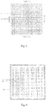
- reference number 21 indicates four sides of a quadrate wafer
- reference 22 indicates dies formed from the quadrate wafer through an existing photolithography process. As shown in Figure 1 , the dies at edges of the quadrate wafer are not intact due to lack of photolithography alignment, which renders waste product.
- JP H07 169673 A discloses that for production of semiconductor lasers circular wafers are of advantage because the wafer material can be utilized to a higher degree than in square wafers. The document further explains alignment technology in connection with circular wafers.
- US 2005/0250291 A1 discloses alignment structure which can be used to align wafers.
- the embodiments relate to circular wafers.
- US 6929888 B2 relates to a photolithography process and corresponding photo masks.
- Mask keys are provided on the photo mask.
- the embodiments relate to the production of LCD arrays, and the alignment keys are provided alongside a single element which is repeated in pattern on a substrate. No particular reference to square wafers is made.
- JP H09 171610 A relates also to align a mask having structure of an element which is to repeated in a pattern on an elongated magnetic strip. No reference to wafers or in particular square wafers is made.
- the invention is defined in claim 1.
- a method of aligning a quadrate wafer during a first photolithography process comprises: step A: fabricating mask aligning markers in a periphery region of a mask, that is used for a first exposure process of the quadrate wafer, with respect to (around) a mask pattern of the mask; step B: during the first exposure process, positioning the quadrate wafer in a preset region by using the mask aligning markers on the mask, and exposing the quadrate wafer by using the mask; and, step C: performing alignment for the quadrate wafer during a second exposure process and subsequent exposure processes by using aligning markers on the quadrate wafer that are obtained during the first exposure process.
- the method of aligning the quadrate wafer with masks according to embodiments of the present invention is simply and reliable, easy to be implemented and may ensure producing completed dies at edges of the quadrate wafer and thus increasing yield of chips.
- the present invention provides a method of aligning a quadrate wafer in a first photolithography process.
- the method includes: step A: fabricating mask aligning markers in a periphery region of a mask, which is used for a first exposure process of the quadrate wafer, around a mask pattern of the mask; step B: during the first exposure process, positioning the quadrate wafer in a preset region by using the mask aligning markers on the mask, and exposing the quadrate wafer through the mask; and step C: performing alignment for the quadrate wafer during a second exposure process and subsequent exposure processes by using aligning markers on the quadrate wafer that are obtained during the first exposure process.
- the method may be easily and reliably performed to ensure intact dies at periphery of a quadrate wafer to be produced and thus render increased yield of chips.
- 21 edge of a quadrate wafer; 22 - incompleted die at periphery of a wafer; 23 - rectangular bar aligning marker; 24 -quadrate-frame aligning marker; 25, 26, 27 - mask pattern.
- Embodiments of the present invention are implemented by forming at least aligning markers at opposite corners of or outside of a quadrate wafer during a preceding photolithography process and performing an aligning process in according with the formed aligning markers during subsequent photolithography processes, ensuring integrity of dies formed at peripheral edges of the quadrate wafer.
- a method of aligning a quadrate wafer with a mask in which the quadrate wafer may be a quadrate GaN-based epitaxial LED-contained wafer.
- a process of manufacturing a LED chip from the epitaxial LED-contained wafer includes a series of processes, such as mesa etching, electrode defining, passivation protecting and the like.
- the method of aligning a quadrate wafer with a mask includes: Step A: fabricating at least two pairs of bar aligning markers parallel to sides of the quadrate wafer respectively in a periphery region of a mask around a mask pattern 25 of the mask, which is used for performing a first exposure on the quadrate wafer, such as, a quadrate GaN-based epitaxial LED wafer, as shown in Figure 5 .
- the bar aligning markers each have a length and a width that may be set as required.
- the inner sides of the pair of bar aligning markers are respectively parallel to sides of the quadrate wafer, and preferably, the bar aligning markers are respectively parallel to two sides of the quadrate wafer that are perpendicular to one another.
- the paired bar aligning markers are perpendicular to one another.
- the aligning marker may be a right-angle or L-shaped aligning marker or a crisscross aligning marker, or a combination thereof.
- the paired bar aligning markers may be perpendicular to one another but not crossed, for example, as shown in Figure 5 .
- the length and width of the bar aligning marker may be configured as required.
- the paired bar aligning markers may be perpendicular to and joint to one another, for example, like the right-angle or L-shaped aligning markers shown in Figure 3 .
- the paired bar aligning markers may be perpendicular to one another and crossed so as to form, for example, a crisscross aligning marker shown in Figure 4 .
- the respective bar aligning markers may be separated from one another.
- the paired bar aligning markers may be jointed to each other.
- the paired bar aligning markers may be crossed to form a crisscross aligning marker.
- At least two pairs of bar aligning markers are configured as two right-angle or L-shaped aligning markers 23, and inner sides of the two right-angle or L-shaped aligning markers 23 are parallel to corresponding sides at two opposite corners of the quadrate GaN-based epitaxial LED-contained wafer, respectively.
- the length and width of the right-angle or L-shaped aligning marker 23 may be set as required, provided that two portions of the right-angle or L-shaped aligning marker perpendicular to each other are respectively parallel to two sides of the quadrate wafer perpendicular to each other. In other words, two bars of the right-angle or L-shaped aligning marker are respectively parallel to two sides of the quadrate wafer perpendicular to each other.
- the right-angle or L-shaped aligning marker shown in Figure 3 is only provided for illustration, but not for limitation.
- the right-angle or L-shaped aligning marker 23 may be modified as a "crisscross" aligning marker with four bars extending in four directions.
- Two bars of the crisscross aligning marker may extend different distances in opposite directions from a cross point of the crisscross aligning marker, as shown in Figure 4 .
- the number of the right-angle or L-shaped bar aligning markers is at least two, that is, there are at least two pairs of bars each having two bars perpendicular to each other.
- the number of the right-angle or L-shaped aligning markers may be three or four. The present invention, however, is not limited to these.
- the inner sides of the right-angle or L-shaped aligning markers are spaced away from corresponding sides of the quadrate GaN-based epitaxial LED-contained wafer to be exposed by a distance in a range from 0 ⁇ m to 100 ⁇ m, or from 0 ⁇ m to 50 ⁇ m, i.e., 0 ⁇ m ⁇ d ⁇ 100 ⁇ m, or 0 ⁇ m ⁇ d ⁇ 50 ⁇ m.
- the aligning marker 23 may be a bar aligning marker, the length of which may be set depending on dimension of the quadrate wafer, such as, a ratio of the length of the bar aligning marker to the length of the side of the quadrate wafer may be in a range from 1/1000 to 1, or in a range from 1/5 to 1.
- the bar aligning markers may be located in a periphery region of the mask around the mask pattern 25, are parallel to sides of the quadrate wafer respectively and are spaced away from sides of the quadrate wafer by a distance d in a range from 0 ⁇ m to 100 ⁇ m.
- Step B during the first exposure process, aligning the inner sides of right-angle or L-shaped aligning marker with two sides at each of two opposite corners of the quadrate GaN-based epitaxial LED-contained wafer and performing exposure on the quadrate GaN-based epitaxial LED-contained wafer with the mask pattern.
- Step C during a second exposure process and subsequent exposure processes, performing alignment of the wafer with mask(s) by an aligning marker on the wafer that is formed in the first photolithography process.
- the photolithography process may be a conventional process.
- a second mask may be aligned by the aligning markers (which are not the right-angle or L-shaped aligning markers in the first mask in above description) formed at corresponding positions of the wafer through the first mask, and the subsequent masks may be aligned in a similar way, thereby ensuring intactness of the dies at periphery of the epitaxial wafer.
- the second mask may be aligned with the epitaxial wafer by means of the aligning markers at positions of the wafer corresponding to the first mask, and so on, thereby ensuring intact dies at periphery of the wafer to be formed and increasing yield of HEMT power device dies.
- the throughout of dies may be increased by 9%.
- alignment and positioning of a wafer may be implemented with naked eye without measuring any dimensions or sizes, thereby largely increasing final yield of the wafer and enhancing convenience.
- a method of aligning a quadrate wafer with a mask wherein the quadrate wafer is a quadrate GaN-based HEMT epitaxial wafer.
- the processes of producing power devices from the GaN-based HEMT epitaxial wafer include a series of photolithography processes for producing source and drain electrodes, mesa etching, and gate electrode.
- the method of aligning a quadrate wafer with a mask includes: Step A': forming a quadrate -frame mask aligning marker 24 on periphery of the mask around mask patterns 26, 27 on the mask, which is used for a first exposure for, such as, a quadrate GaN-based HEMT epitaxial wafer, inner sides of the quadrate -frame mask aligning marker 24 corresponding to edges of the quadrate GaN-based HEMT epitaxial wafer, as shown in Figure 4 .
- the quadrate -frame mask aligning marker 24 is another embodiment of the present invention. It is appreciated by those skilled in the art that, based on the embodiments of the present invention, the bar aligning markers may be in a separated arrangement as in the first embodiment of the present invention, or may be jointed with one another as in the second embodiment of the present invention.
- a width of the quadrate-frame mask aligning marker 24 may be set as required, provided that two parts of the quadrate-frame mask aligning marker 24 perpendicular to one another, are respectively parallel to two sides, which are perpendicular to one another, of the quadrate wafer.
- the inner sides of the quadrate -frame mask aligning marker may be the same as, or may be slightly bigger than corresponding edges of the quadrate GaN-based epitaxial LED-contained wafer, wherein, the distance d between the inner sides of the quadrate-frame mask aligning marker and corresponding edges of the quadrate GaN-based HEMT epitaxial wafer may be in range from 0 ⁇ m to 100 ⁇ m.
- Step B' during the first exposure process, aligning the quadrate-frame mask aligning markers at periphery of the mask with the edges of the quadrate GaN-based HEMT epitaxial wafer and performing the first exposure with the mask pattern of the mask on the quadrate GaN-based HEMT epitaxial wafer.
- Step C' during a second exposure process and subsequent exposure, performing subsequent alignment of the wafer with mask(s) by using the aligning markers formed on the wafer during the first photolithography process.
- the photolithography processes may be implemented according to common photolithography processes in prior art.
- the aligning markers Through the aligning markers, it ensures intact source and drain electrodes of dies at periphery of the quadrate GaN-based HEMT epitaxial wafer.
- the second mask may be aligned with the epitaxial wafer with the aligning markers formed at positions of the wafer corresponding to the aligning markers on the first mask, and so on, thereby ensuring intact dies at periphery of the wafer to be formed and increasing yield of dies for HEMT power devices.
- the quadrate wafer may be made of GaN, Si, SiC, GaAs, AlGaInP or GaP; (2) the quadrate wafer may be processed to produce devices, such as, LED, laser device, photodetector, solar cell, and the like.
- a method of aligning a quadrate wafer with a mask particularly the method according to preferred embodiment of the present invention, which largely improves operation convenience during alignment and is simple and reliable and easy to be implemented.
- the method may be performed to ensure intact dies at periphery of a quadrate wafer to be produced and increases yield of chips.
Landscapes
- Physics & Mathematics (AREA)
- General Physics & Mathematics (AREA)
- Exposure And Positioning Against Photoresist Photosensitive Materials (AREA)
- Preparing Plates And Mask In Photomechanical Process (AREA)
Description
- The present invention relates to semiconductor technology field, and particularly to a method of aligning a quadrate wafer during a first photolithography process.
- It is common that only a quadrate or rectangular die can be produced due to limitation from cutting a wafer during manufacturing dies from the wafer, which renders waste during cutting a circular wafer in virtue of cutting lots of incompleted dies at periphery of the wafer. By comparison, for a quadrate or rectangular wafer, no incompleted die is formed during cutting the quadrate wafer as the edges of the quadrate wafer are parallel to a cutting direction and are different from the arc edge of the circular wafer.
- During manufacturing dies from a wafer, a plurality of processes are needed, including mesa etching, electrode defining, passivation protecting, and thus a series of mask patterns for various processes are needed. As for a circular wafer, it can be exposed under a first mask directly since it is not needed to be aligned to the mask during a first exposure process. A second mask may be aligned to the wafer according to a formed aligning marker formed at a corresponding position of the wafer through the first mask, and so on. However, it is impossible to ensure integrity of dies formed at edges of a quadrate wafer by implementing the above photolithography mask alignment way. As shown in
Figure 1 ,reference number 21 indicates four sides of a quadrate wafer, andreference 22 indicates dies formed from the quadrate wafer through an existing photolithography process. As shown inFigure 1 , the dies at edges of the quadrate wafer are not intact due to lack of photolithography alignment, which renders waste product. -
JP H07 169673 A -
US 2005/0250291 A1 discloses alignment structure which can be used to align wafers. The embodiments relate to circular wafers. -
US 6929888 B2 relates to a photolithography process and corresponding photo masks. Mask keys are provided on the photo mask. The embodiments relate to the production of LCD arrays, and the alignment keys are provided alongside a single element which is repeated in pattern on a substrate. No particular reference to square wafers is made. -
JP H09 171610 A - Aiming to solve the above problems, it is an object to provide a method of aligning a quadrate wafer during a first photolithography process in order to avoid damage to dies due to exposure processes.
- The invention is defined in claim 1.
- According to an aspect, there is provided a method of aligning a quadrate wafer during a first photolithography process. The method comprises: step A: fabricating mask aligning markers in a periphery region of a mask, that is used for a first exposure process of the quadrate wafer, with respect to (around) a mask pattern of the mask; step B: during the first exposure process, positioning the quadrate wafer in a preset region by using the mask aligning markers on the mask, and exposing the quadrate wafer by using the mask; and, step C: performing alignment for the quadrate wafer during a second exposure process and subsequent exposure processes by using aligning markers on the quadrate wafer that are obtained during the first exposure process.
- The method of aligning the quadrate wafer with masks according to embodiments of the present invention is simply and reliable, easy to be implemented and may ensure producing completed dies at edges of the quadrate wafer and thus increasing yield of chips.
- The present invention provides a method of aligning a quadrate wafer in a first photolithography process. The method includes: step A: fabricating mask aligning markers in a periphery region of a mask, which is used for a first exposure process of the quadrate wafer, around a mask pattern of the mask; step B: during the first exposure process, positioning the quadrate wafer in a preset region by using the mask aligning markers on the mask, and exposing the quadrate wafer through the mask; and step C: performing alignment for the quadrate wafer during a second exposure process and subsequent exposure processes by using aligning markers on the quadrate wafer that are obtained during the first exposure process. The method may be easily and reliably performed to ensure intact dies at periphery of a quadrate wafer to be produced and thus render increased yield of chips.
-
Figure 1 shows distribution of dies on a quadrate wafer after exposure in a first photolithography process, in which the quadrate wafer is not aligned to a mask used in the first photolithography process; -
Figure 2 is a flow chart of a method of aligning a quadrate wafer with a mask during exposure in a first photolithography process according to an embodiment of the present invention; -
Figure 3 is a schematic view of the mask used in the first photolithography process of the method illustrated inFigure 2 ; -
Figure 4 is an another schematic view of the mask used in the first photolithography process of the method illustrated inFigure 2 ; -
Figure 5 is a further schematic view of the mask used in the first photolithography process of the method illustrated inFigure 2 ; and -
Figure 6 is a schematic view of the mask used in the first photolithography process according to another embodiment of the present invention. - 21 -edge of a quadrate wafer; 22 - incompleted die at periphery of a wafer; 23 - rectangular bar aligning marker; 24 -quadrate-frame aligning marker; 25, 26, 27 - mask pattern.
- In order to make the purposes, technical solutions and advantages of the present invention clearer, the present invention are further described in detail in conjunction with embodiments with reference to the drawings. It is noted that similar or same components are referred by similar reference sign in drawings or specification. The embodiments that are not illustrated or described in the specification may be known by those skilled in the art. In addition, it is appreciated that specific values of parameters in the text are provided for illustration, rather than for defining specific values of the parameters. In the embodiments, directional terms, such as upper, lower, forward, backward, left and right, are only used for directions in the drawings. Thus, the directional terms are not used for limiting the protective scope of the present invention.
- Embodiments of the present invention are implemented by forming at least aligning markers at opposite corners of or outside of a quadrate wafer during a preceding photolithography process and performing an aligning process in according with the formed aligning markers during subsequent photolithography processes, ensuring integrity of dies formed at peripheral edges of the quadrate wafer.
- In a first embodiment of the present invention, there is provided a method of aligning a quadrate wafer with a mask, in which the quadrate wafer may be a quadrate GaN-based epitaxial LED-contained wafer. A process of manufacturing a LED chip from the epitaxial LED-contained wafer includes a series of processes, such as mesa etching, electrode defining, passivation protecting and the like.
- Referring to
Figure 2 , the method of aligning a quadrate wafer with a mask includes:
Step A: fabricating at least two pairs of bar aligning markers parallel to sides of the quadrate wafer respectively in a periphery region of a mask around amask pattern 25 of the mask, which is used for performing a first exposure on the quadrate wafer, such as, a quadrate GaN-based epitaxial LED wafer, as shown inFigure 5 . The bar aligning markers each have a length and a width that may be set as required. The inner sides of the pair of bar aligning markers are respectively parallel to sides of the quadrate wafer, and preferably, the bar aligning markers are respectively parallel to two sides of the quadrate wafer that are perpendicular to one another. Further, the paired bar aligning markers are perpendicular to one another. Particularly, the aligning marker may be a right-angle or L-shaped aligning marker or a crisscross aligning marker, or a combination thereof. In one example, the paired bar aligning markers may be perpendicular to one another but not crossed, for example, as shown inFigure 5 . The length and width of the bar aligning marker may be configured as required. In another example, the paired bar aligning markers may be perpendicular to and joint to one another, for example, like the right-angle or L-shaped aligning markers shown inFigure 3 . Alternatively, the paired bar aligning markers may be perpendicular to one another and crossed so as to form, for example, a crisscross aligning marker shown inFigure 4 . - According to an embodiment of the present invention, the respective bar aligning markers may be separated from one another. According to an embodiment of the present invention, the paired bar aligning markers may be jointed to each other. According to an embodiment of the present invention, the paired bar aligning markers may be crossed to form a crisscross aligning marker. Those skilled in the art may obtain other arrangements of the bar aligning markers as required, provided that the bar aligning markers are provided to be parallel to corresponding sides of the wafer to achieve alignment purpose.
- In a preferred embodiment of the present invention, at least two pairs of bar aligning markers are configured as two right-angle or L-shaped aligning
markers 23, and inner sides of the two right-angle or L-shaped aligningmarkers 23 are parallel to corresponding sides at two opposite corners of the quadrate GaN-based epitaxial LED-contained wafer, respectively. - It is noted that the length and width of the right-angle or L-shaped aligning
marker 23 may be set as required, provided that two portions of the right-angle or L-shaped aligning marker perpendicular to each other are respectively parallel to two sides of the quadrate wafer perpendicular to each other. In other words, two bars of the right-angle or L-shaped aligning marker are respectively parallel to two sides of the quadrate wafer perpendicular to each other. The right-angle or L-shaped aligning marker shown inFigure 3 is only provided for illustration, but not for limitation. The right-angle or L-shaped aligning marker 23 may be modified as a "crisscross" aligning marker with four bars extending in four directions. Two bars of the crisscross aligning marker may extend different distances in opposite directions from a cross point of the crisscross aligning marker, as shown inFigure 4 . For example, the number of the right-angle or L-shaped bar aligning markers is at least two, that is, there are at least two pairs of bars each having two bars perpendicular to each other. For example, the number of the right-angle or L-shaped aligning markers may be three or four. The present invention, however, is not limited to these. The inner sides of the right-angle or L-shaped aligning markers are spaced away from corresponding sides of the quadrate GaN-based epitaxial LED-contained wafer to be exposed by a distance in a range from 0µm to 100µm, or from 0µm to 50µm, i.e., 0µm ≤d ≤100µm, or 0µm≤d≤50µm. - In addition, as shown in
Figure 5 , the aligningmarker 23 may be a bar aligning marker, the length of which may be set depending on dimension of the quadrate wafer, such as, a ratio of the length of the bar aligning marker to the length of the side of the quadrate wafer may be in a range from 1/1000 to 1, or in a range from 1/5 to 1. The bar aligning markers may be located in a periphery region of the mask around themask pattern 25, are parallel to sides of the quadrate wafer respectively and are spaced away from sides of the quadrate wafer by a distance d in a range from 0µm to 100µm. - Step B: during the first exposure process, aligning the inner sides of right-angle or L-shaped aligning marker with two sides at each of two opposite corners of the quadrate GaN-based epitaxial LED-contained wafer and performing exposure on the quadrate GaN-based epitaxial LED-contained wafer with the mask pattern.
- Step C: during a second exposure process and subsequent exposure processes, performing alignment of the wafer with mask(s) by an aligning marker on the wafer that is formed in the first photolithography process.
- In the embodiment, the photolithography process may be a conventional process.
- As the die mesa at periphery of the epitaxial wafer is maintained intact after the first photolithography process, a second mask may be aligned by the aligning markers (which are not the right-angle or L-shaped aligning markers in the first mask in above description) formed at corresponding positions of the wafer through the first mask, and the subsequent masks may be aligned in a similar way, thereby ensuring intactness of the dies at periphery of the epitaxial wafer. As die mesa at periphery of the epitaxial wafer is intact after the first photolithography process, the second mask may be aligned with the epitaxial wafer by means of the aligning markers at positions of the wafer corresponding to the first mask, and so on, thereby ensuring intact dies at periphery of the wafer to be formed and increasing yield of HEMT power device dies. For example, for a 2-inches quadrate epitaxial LED-contained wafer including 45 million dies, the throughout of dies may be increased by 9%. In practice, since alignment is implemented in micro scale, it is a time-and-labor consuming process to implement alignment using specific dimensions. According to the embodiments of the present invention, alignment and positioning of a wafer may be implemented with naked eye without measuring any dimensions or sizes, thereby largely increasing final yield of the wafer and enhancing convenience.
- In a second exemplary embodiment of the present invention, there is provided a method of aligning a quadrate wafer with a mask, wherein the quadrate wafer is a quadrate GaN-based HEMT epitaxial wafer. The processes of producing power devices from the GaN-based HEMT epitaxial wafer include a series of photolithography processes for producing source and drain electrodes, mesa etching, and gate electrode.
- As shown in
Figure 6 , the method of aligning a quadrate wafer with a mask includes:
Step A': forming a quadrate -framemask aligning marker 24 on periphery of the mask around mask patterns 26, 27 on the mask, which is used for a first exposure for, such as, a quadrate GaN-based HEMT epitaxial wafer, inner sides of the quadrate -framemask aligning marker 24 corresponding to edges of the quadrate GaN-based HEMT epitaxial wafer, as shown inFigure 4 . The quadrate -framemask aligning marker 24 is another embodiment of the present invention. It is appreciated by those skilled in the art that, based on the embodiments of the present invention, the bar aligning markers may be in a separated arrangement as in the first embodiment of the present invention, or may be jointed with one another as in the second embodiment of the present invention. - It is noted that a width of the quadrate-frame
mask aligning marker 24 may be set as required, provided that two parts of the quadrate-framemask aligning marker 24 perpendicular to one another, are respectively parallel to two sides, which are perpendicular to one another, of the quadrate wafer. In addition, the inner sides of the quadrate -frame mask aligning marker may be the same as, or may be slightly bigger than corresponding edges of the quadrate GaN-based epitaxial LED-contained wafer, wherein, the distance d between the inner sides of the quadrate-frame mask aligning marker and corresponding edges of the quadrate GaN-based HEMT epitaxial wafer may be in range from 0 µm to 100 µm. - Step B': during the first exposure process, aligning the quadrate-frame mask aligning markers at periphery of the mask with the edges of the quadrate GaN-based HEMT epitaxial wafer and performing the first exposure with the mask pattern of the mask on the quadrate GaN-based HEMT epitaxial wafer.
- Step C': during a second exposure process and subsequent exposure, performing subsequent alignment of the wafer with mask(s) by using the aligning markers formed on the wafer during the first photolithography process.
- In the embodiment, the photolithography processes may be implemented according to common photolithography processes in prior art. Through the aligning markers, it ensures intact source and drain electrodes of dies at periphery of the quadrate GaN-based HEMT epitaxial wafer. According to conventional photolithography processes, as die mesa at periphery of the epitaxial wafer is intact after the first photolithography process, the second mask may be aligned with the epitaxial wafer with the aligning markers formed at positions of the wafer corresponding to the aligning markers on the first mask, and so on, thereby ensuring intact dies at periphery of the wafer to be formed and increasing yield of dies for HEMT power devices.
- Two embodiments of the present invention are described in detailed with reference to the drawings. Those skilled in the art may obtain clear understanding on the method of aligning a quadrate wafer with a mask according to embodiments of the present invention.
- In addition, definition of various components and methods are not limited to the specific structures, shapes and approaches described in the above embodiments, but may be modified or replaced by those skilled in the art based on common knowledge. For example, (1) the quadrate wafer may be made of GaN, Si, SiC, GaAs, AlGaInP or GaP; (2) the quadrate wafer may be processed to produce devices, such as, LED, laser device, photodetector, solar cell, and the like.
- In sum, there is provided a method of aligning a quadrate wafer with a mask, particularly the method according to preferred embodiment of the present invention, which largely improves operation convenience during alignment and is simple and reliable and easy to be implemented. The method may be performed to ensure intact dies at periphery of a quadrate wafer to be produced and increases yield of chips.
- The above embodiments are described to illustrate the purposes, technique solutions and advantageous effects of the present invention. It is understood that the above description is only provided for describing the embodiments of the present invention, and not for limiting the invention. The scope of the invention is defined by the appended claims.
Claims (11)
- A method of aligning a quadrate wafer in a first photolithography process, comprising:step A: fabricating mask aligning markers (23, 24) in a periphery region of a mask, which is used for a first exposure process of the quadrate wafer, around a mask pattern (25, 26, 27) of the mask;step B: during the first exposure process, positioning the quadrate wafer in a preset region by using the mask aligning markers (23, 24) on the mask, and exposing the quadrate wafer through the mask; andstep C: performing alignment for the quadrate wafer during a second exposure process and subsequent exposure processes by using aligning markers on the quadrate wafer that are obtained during the first exposure process,wherein the mask aligning markers includes bars (23) that are parallel to sides of the quadrate wafer respectively.
- The method according to claim 1, wherein the aligning markers include at least two pairs of bars (23).
- The method according to claim 2, wherein each pair of bars (23) are configured as a right-angle shaped aligning marker or a crisscross aligning marker.
- The method according to claim 3, wherein inner sides of at least two right-angle shaped aligning markers or at least two crisscross aligning markers (23) are parallel to sides at at least two corners of the quadrate wafer respectively.
- The method according to claim 2, wherein four bars of two pairs of bars (23) are connected to form a quadrate-frame, or are separated from one another.
- The method according to claim 3, wherein the aligning markers includes two, three or four right-angle shaped aligning markers (23) or crisscross aligning markers (23).
- The method according to claim 3, wherein the aligning markers include two right-angle shaped aligning markers (23) each comprising a pair of bars, the bars of each of the two right-angle shaped aligning markers being respectively aligned with sides of a corresponding one of two opposite corners of the quadrate wafer.
- The method according to claim 1, wherein the aligning markers are configured as a quadrate-frame aligning marker (24);
inner sides of the quadrate-frame aligning marker (24) are parallel to peripheral edges of the quadrate wafer respectively. - The method according to claim 2, wherein inner sides of the aligning markers are spaced from respective edges of the quadrate wafer by a distance d in a range from 0µm to 50µm.
- The method according to claim 1, wherein the quadrate wafer is made of GaN, Si, SiC, GaAs, AlGaInP or GaP.
- The method according to claim 1, wherein the method is implemented when producing a LED, a laser, a photoelectric detector or a solar cell device.
Applications Claiming Priority (2)
| Application Number | Priority Date | Filing Date | Title |
|---|---|---|---|
| CN201310485162.4A CN103529658B (en) | 2013-10-16 | 2013-10-16 | Method for aligning square wafer in primary photolithography technique |
| PCT/CN2014/070051 WO2015054977A1 (en) | 2013-10-16 | 2014-01-03 | Method for aligning square wafer in first photolithographic process |
Publications (3)
| Publication Number | Publication Date |
|---|---|
| EP3059635A1 EP3059635A1 (en) | 2016-08-24 |
| EP3059635A4 EP3059635A4 (en) | 2017-06-07 |
| EP3059635B1 true EP3059635B1 (en) | 2019-05-08 |
Family
ID=49931770
Family Applications (1)
| Application Number | Title | Priority Date | Filing Date |
|---|---|---|---|
| EP14853966.1A Active EP3059635B1 (en) | 2013-10-16 | 2014-01-03 | Method for aligning quadrate wafer in first photolithographic process |
Country Status (4)
| Country | Link |
|---|---|
| US (1) | US9791790B2 (en) |
| EP (1) | EP3059635B1 (en) |
| CN (1) | CN103529658B (en) |
| WO (1) | WO2015054977A1 (en) |
Families Citing this family (9)
| Publication number | Priority date | Publication date | Assignee | Title |
|---|---|---|---|---|
| CN105988311B (en) * | 2015-03-03 | 2018-03-16 | 中芯国际集成电路制造(上海)有限公司 | A kind of alignment patterns and preparation method thereof |
| KR102392043B1 (en) * | 2015-05-06 | 2022-04-28 | 삼성디스플레이 주식회사 | Display substrate exposure method |
| CN105527800B (en) * | 2016-02-18 | 2017-07-18 | 京东方科技集团股份有限公司 | A kind of exposure method, exposure device and color membrane substrates |
| CN110221517A (en) * | 2018-03-02 | 2019-09-10 | 长鑫存储技术有限公司 | Measurement markers and photomask with the measurement markers |
| CN108735645A (en) * | 2018-05-24 | 2018-11-02 | 德淮半导体有限公司 | Wafer alignment method and wafer alignment device |
| US11009798B2 (en) | 2018-09-05 | 2021-05-18 | Micron Technology, Inc. | Wafer alignment markers, systems, and related methods |
| US11251096B2 (en) | 2018-09-05 | 2022-02-15 | Micron Technology, Inc. | Wafer registration and overlay measurement systems and related methods |
| CN113219797B (en) * | 2021-03-25 | 2023-11-17 | 北海惠科半导体科技有限公司 | Wafer semiconductor product and manufacturing method thereof |
| CN113448181A (en) * | 2021-07-29 | 2021-09-28 | 苏州工业园区纳米产业技术研究院有限公司 | Alignment method for double exposure |
Family Cites Families (15)
| Publication number | Priority date | Publication date | Assignee | Title |
|---|---|---|---|---|
| JPS6255655A (en) * | 1985-09-03 | 1987-03-11 | Matsushita Electric Ind Co Ltd | Photomask |
| JPH07169673A (en) * | 1993-12-15 | 1995-07-04 | Mitsubishi Electric Corp | Manufacture of optical device |
| JPH07249558A (en) * | 1994-03-09 | 1995-09-26 | Nikon Corp | Alignment method |
| JPH09171610A (en) * | 1995-08-18 | 1997-06-30 | Nikon Corp | Method for aligning rectangular substrate |
| KR100611041B1 (en) * | 2000-02-17 | 2006-08-09 | 엘지.필립스 엘시디 주식회사 | photo mask and method for fabricating large scale liquid crystal display device |
| US20050250291A1 (en) * | 2004-05-06 | 2005-11-10 | Pary Baluswamy | Methods for clearing alignment markers useable in semiconductor lithography |
| JP4854998B2 (en) * | 2005-07-05 | 2012-01-18 | 三菱電機株式会社 | Manufacturing method of liquid crystal display device |
| US20070108638A1 (en) * | 2005-11-16 | 2007-05-17 | International Business Machines Corporation | Alignment mark with improved resistance to dicing induced cracking and delamination in the scribe region |
| JP5023653B2 (en) * | 2006-10-19 | 2012-09-12 | 富士通セミコンダクター株式会社 | EXPOSURE MASK, ELECTRONIC DEVICE MANUFACTURING METHOD, AND EXPOSURE MASK INSPECTING METHOD |
| CN101369571B (en) * | 2007-08-17 | 2010-06-09 | 中芯国际集成电路制造(上海)有限公司 | Semiconductor device, wafer coarse alignment mark and coarse alignment method |
| CN101458443A (en) * | 2007-12-13 | 2009-06-17 | 中芯国际集成电路制造(上海)有限公司 | Photo mask, method for producing the same and graphic method |
| JP5605102B2 (en) * | 2010-09-07 | 2014-10-15 | 住友電気工業株式会社 | Manufacturing method of semiconductor laser device |
| JP5933289B2 (en) * | 2012-02-23 | 2016-06-08 | 三菱電機株式会社 | SOI wafer and manufacturing method thereof |
| CN103293867B (en) * | 2012-03-05 | 2015-07-22 | 上海微电子装备有限公司 | Pre-alignment device and method of square substrates |
| CN102799062A (en) * | 2012-08-29 | 2012-11-28 | 上海宏力半导体制造有限公司 | Mask, wafer and monitor method |
-
2013
- 2013-10-16 CN CN201310485162.4A patent/CN103529658B/en active Active
-
2014
- 2014-01-03 WO PCT/CN2014/070051 patent/WO2015054977A1/en active Application Filing
- 2014-01-03 EP EP14853966.1A patent/EP3059635B1/en active Active
- 2014-01-03 US US14/901,541 patent/US9791790B2/en active Active
Non-Patent Citations (1)
| Title |
|---|
| None * |
Also Published As
| Publication number | Publication date |
|---|---|
| US20160170317A1 (en) | 2016-06-16 |
| EP3059635A1 (en) | 2016-08-24 |
| EP3059635A4 (en) | 2017-06-07 |
| WO2015054977A1 (en) | 2015-04-23 |
| US9791790B2 (en) | 2017-10-17 |
| CN103529658B (en) | 2015-04-01 |
| CN103529658A (en) | 2014-01-22 |
Similar Documents
| Publication | Publication Date | Title |
|---|---|---|
| EP3059635B1 (en) | Method for aligning quadrate wafer in first photolithographic process | |
| JP4278645B2 (en) | Semiconductor wafer, layout setting method thereof, and reticle layout setting method | |
| JP5560931B2 (en) | Manufacturing method of super junction semiconductor device | |
| JP5560897B2 (en) | Manufacturing method of super junction semiconductor device | |
| JP2010529685A5 (en) | ||
| US7755207B2 (en) | Wafer, reticle, and exposure method using the wafer and reticle | |
| TWI420584B (en) | Semiconductor wafer and method for cutting the same | |
| CN106298464B (en) | The method of cut crystal | |
| DE102014112690B4 (en) | Process for separating semiconductor chips | |
| CN103065929B (en) | Manufacture method of alignment mark protective layer | |
| WO2019012499A8 (en) | Method for the alignment of photolithographic masks and corresponding process for manufacturing integrated circuits in a wafer of semiconductor material | |
| CN104023932A (en) | Method for producing lens array, and molding mold | |
| CN112071824A (en) | Grating device mask and manufacturing method | |
| US11605550B2 (en) | Alignment system | |
| JP2012089540A (en) | Method of manufacturing semiconductor device | |
| CN101986427A (en) | Semiconductor wafer having pre-aligning pattern and method for pre-aligning the same | |
| CN112130414B (en) | Calibration method for feeding position of photolithography mask and exposure machine | |
| JP2013021040A (en) | Silicon carbide semiconductor device manufacturing method and silicon carbide semiconductor device | |
| CN105988292A (en) | Photoresist with atypical pattern and method for etching substrate and forming hole | |
| CN111564370A (en) | Groove type power device and manufacturing method thereof | |
| KR20160104561A (en) | Magnetic sensor and method of manufacturing the same | |
| JP2009282386A (en) | Photomask and method for manufacturing for semiconductor chip | |
| US9536838B1 (en) | Single crystal ingot, semiconductor wafer and method of manufacturing semiconductor wafers | |
| CN105810556B (en) | For the reticle of etching groove and the lithographic method of groove | |
| US10679940B2 (en) | Mask and metal wiring of a semiconductor device formed using the same |
Legal Events
| Date | Code | Title | Description |
|---|---|---|---|
| PUAI | Public reference made under article 153(3) epc to a published international application that has entered the european phase |
Free format text: ORIGINAL CODE: 0009012 |
|
| 17P | Request for examination filed |
Effective date: 20160415 |
|
| AK | Designated contracting states |
Kind code of ref document: A1 Designated state(s): AL AT BE BG CH CY CZ DE DK EE ES FI FR GB GR HR HU IE IS IT LI LT LU LV MC MK MT NL NO PL PT RO RS SE SI SK SM TR |
|
| AX | Request for extension of the european patent |
Extension state: BA ME |
|
| DAX | Request for extension of the european patent (deleted) | ||
| A4 | Supplementary search report drawn up and despatched |
Effective date: 20170508 |
|
| RIC1 | Information provided on ipc code assigned before grant |
Ipc: G03F 1/42 20120101ALI20170428BHEP Ipc: G03F 9/00 20060101AFI20170428BHEP |
|
| GRAP | Despatch of communication of intention to grant a patent |
Free format text: ORIGINAL CODE: EPIDOSNIGR1 |
|
| STAA | Information on the status of an ep patent application or granted ep patent |
Free format text: STATUS: GRANT OF PATENT IS INTENDED |
|
| INTG | Intention to grant announced |
Effective date: 20181220 |
|
| GRAS | Grant fee paid |
Free format text: ORIGINAL CODE: EPIDOSNIGR3 |
|
| GRAA | (expected) grant |
Free format text: ORIGINAL CODE: 0009210 |
|
| STAA | Information on the status of an ep patent application or granted ep patent |
Free format text: STATUS: THE PATENT HAS BEEN GRANTED |
|
| AK | Designated contracting states |
Kind code of ref document: B1 Designated state(s): AL AT BE BG CH CY CZ DE DK EE ES FI FR GB GR HR HU IE IS IT LI LT LU LV MC MK MT NL NO PL PT RO RS SE SI SK SM TR |
|
| REG | Reference to a national code |
Ref country code: GB Ref legal event code: FG4D |
|
| REG | Reference to a national code |
Ref country code: CH Ref legal event code: EP Ref country code: AT Ref legal event code: REF Ref document number: 1131130 Country of ref document: AT Kind code of ref document: T Effective date: 20190515 |
|
| REG | Reference to a national code |
Ref country code: DE Ref legal event code: R096 Ref document number: 602014046577 Country of ref document: DE Ref country code: IE Ref legal event code: FG4D |
|
| REG | Reference to a national code |
Ref country code: NL Ref legal event code: FP |
|
| REG | Reference to a national code |
Ref country code: LT Ref legal event code: MG4D |
|
| PG25 | Lapsed in a contracting state [announced via postgrant information from national office to epo] |
Ref country code: HR Free format text: LAPSE BECAUSE OF FAILURE TO SUBMIT A TRANSLATION OF THE DESCRIPTION OR TO PAY THE FEE WITHIN THE PRESCRIBED TIME-LIMIT Effective date: 20190508 Ref country code: SE Free format text: LAPSE BECAUSE OF FAILURE TO SUBMIT A TRANSLATION OF THE DESCRIPTION OR TO PAY THE FEE WITHIN THE PRESCRIBED TIME-LIMIT Effective date: 20190508 Ref country code: PT Free format text: LAPSE BECAUSE OF FAILURE TO SUBMIT A TRANSLATION OF THE DESCRIPTION OR TO PAY THE FEE WITHIN THE PRESCRIBED TIME-LIMIT Effective date: 20190908 Ref country code: NO Free format text: LAPSE BECAUSE OF FAILURE TO SUBMIT A TRANSLATION OF THE DESCRIPTION OR TO PAY THE FEE WITHIN THE PRESCRIBED TIME-LIMIT Effective date: 20190808 Ref country code: AL Free format text: LAPSE BECAUSE OF FAILURE TO SUBMIT A TRANSLATION OF THE DESCRIPTION OR TO PAY THE FEE WITHIN THE PRESCRIBED TIME-LIMIT Effective date: 20190508 Ref country code: FI Free format text: LAPSE BECAUSE OF FAILURE TO SUBMIT A TRANSLATION OF THE DESCRIPTION OR TO PAY THE FEE WITHIN THE PRESCRIBED TIME-LIMIT Effective date: 20190508 Ref country code: LT Free format text: LAPSE BECAUSE OF FAILURE TO SUBMIT A TRANSLATION OF THE DESCRIPTION OR TO PAY THE FEE WITHIN THE PRESCRIBED TIME-LIMIT Effective date: 20190508 Ref country code: ES Free format text: LAPSE BECAUSE OF FAILURE TO SUBMIT A TRANSLATION OF THE DESCRIPTION OR TO PAY THE FEE WITHIN THE PRESCRIBED TIME-LIMIT Effective date: 20190508 |
|
| PG25 | Lapsed in a contracting state [announced via postgrant information from national office to epo] |
Ref country code: GR Free format text: LAPSE BECAUSE OF FAILURE TO SUBMIT A TRANSLATION OF THE DESCRIPTION OR TO PAY THE FEE WITHIN THE PRESCRIBED TIME-LIMIT Effective date: 20190809 Ref country code: BG Free format text: LAPSE BECAUSE OF FAILURE TO SUBMIT A TRANSLATION OF THE DESCRIPTION OR TO PAY THE FEE WITHIN THE PRESCRIBED TIME-LIMIT Effective date: 20190808 Ref country code: RS Free format text: LAPSE BECAUSE OF FAILURE TO SUBMIT A TRANSLATION OF THE DESCRIPTION OR TO PAY THE FEE WITHIN THE PRESCRIBED TIME-LIMIT Effective date: 20190508 Ref country code: LV Free format text: LAPSE BECAUSE OF FAILURE TO SUBMIT A TRANSLATION OF THE DESCRIPTION OR TO PAY THE FEE WITHIN THE PRESCRIBED TIME-LIMIT Effective date: 20190508 |
|
| REG | Reference to a national code |
Ref country code: AT Ref legal event code: MK05 Ref document number: 1131130 Country of ref document: AT Kind code of ref document: T Effective date: 20190508 |
|
| PG25 | Lapsed in a contracting state [announced via postgrant information from national office to epo] |
Ref country code: DK Free format text: LAPSE BECAUSE OF FAILURE TO SUBMIT A TRANSLATION OF THE DESCRIPTION OR TO PAY THE FEE WITHIN THE PRESCRIBED TIME-LIMIT Effective date: 20190508 Ref country code: AT Free format text: LAPSE BECAUSE OF FAILURE TO SUBMIT A TRANSLATION OF THE DESCRIPTION OR TO PAY THE FEE WITHIN THE PRESCRIBED TIME-LIMIT Effective date: 20190508 Ref country code: EE Free format text: LAPSE BECAUSE OF FAILURE TO SUBMIT A TRANSLATION OF THE DESCRIPTION OR TO PAY THE FEE WITHIN THE PRESCRIBED TIME-LIMIT Effective date: 20190508 Ref country code: RO Free format text: LAPSE BECAUSE OF FAILURE TO SUBMIT A TRANSLATION OF THE DESCRIPTION OR TO PAY THE FEE WITHIN THE PRESCRIBED TIME-LIMIT Effective date: 20190508 Ref country code: CZ Free format text: LAPSE BECAUSE OF FAILURE TO SUBMIT A TRANSLATION OF THE DESCRIPTION OR TO PAY THE FEE WITHIN THE PRESCRIBED TIME-LIMIT Effective date: 20190508 Ref country code: SK Free format text: LAPSE BECAUSE OF FAILURE TO SUBMIT A TRANSLATION OF THE DESCRIPTION OR TO PAY THE FEE WITHIN THE PRESCRIBED TIME-LIMIT Effective date: 20190508 |
|
| REG | Reference to a national code |
Ref country code: DE Ref legal event code: R097 Ref document number: 602014046577 Country of ref document: DE |
|
| PG25 | Lapsed in a contracting state [announced via postgrant information from national office to epo] |
Ref country code: SM Free format text: LAPSE BECAUSE OF FAILURE TO SUBMIT A TRANSLATION OF THE DESCRIPTION OR TO PAY THE FEE WITHIN THE PRESCRIBED TIME-LIMIT Effective date: 20190508 Ref country code: IT Free format text: LAPSE BECAUSE OF FAILURE TO SUBMIT A TRANSLATION OF THE DESCRIPTION OR TO PAY THE FEE WITHIN THE PRESCRIBED TIME-LIMIT Effective date: 20190508 |
|
| PLBE | No opposition filed within time limit |
Free format text: ORIGINAL CODE: 0009261 |
|
| STAA | Information on the status of an ep patent application or granted ep patent |
Free format text: STATUS: NO OPPOSITION FILED WITHIN TIME LIMIT |
|
| PG25 | Lapsed in a contracting state [announced via postgrant information from national office to epo] |
Ref country code: TR Free format text: LAPSE BECAUSE OF FAILURE TO SUBMIT A TRANSLATION OF THE DESCRIPTION OR TO PAY THE FEE WITHIN THE PRESCRIBED TIME-LIMIT Effective date: 20190508 |
|
| 26N | No opposition filed |
Effective date: 20200211 |
|
| PG25 | Lapsed in a contracting state [announced via postgrant information from national office to epo] |
Ref country code: PL Free format text: LAPSE BECAUSE OF FAILURE TO SUBMIT A TRANSLATION OF THE DESCRIPTION OR TO PAY THE FEE WITHIN THE PRESCRIBED TIME-LIMIT Effective date: 20190508 |
|
| PG25 | Lapsed in a contracting state [announced via postgrant information from national office to epo] |
Ref country code: SI Free format text: LAPSE BECAUSE OF FAILURE TO SUBMIT A TRANSLATION OF THE DESCRIPTION OR TO PAY THE FEE WITHIN THE PRESCRIBED TIME-LIMIT Effective date: 20190508 |
|
| PG25 | Lapsed in a contracting state [announced via postgrant information from national office to epo] |
Ref country code: MC Free format text: LAPSE BECAUSE OF FAILURE TO SUBMIT A TRANSLATION OF THE DESCRIPTION OR TO PAY THE FEE WITHIN THE PRESCRIBED TIME-LIMIT Effective date: 20190508 |
|
| REG | Reference to a national code |
Ref country code: CH Ref legal event code: PL |
|
| REG | Reference to a national code |
Ref country code: BE Ref legal event code: MM Effective date: 20200131 |
|
| PG25 | Lapsed in a contracting state [announced via postgrant information from national office to epo] |
Ref country code: LU Free format text: LAPSE BECAUSE OF NON-PAYMENT OF DUE FEES Effective date: 20200103 |
|
| PG25 | Lapsed in a contracting state [announced via postgrant information from national office to epo] |
Ref country code: LI Free format text: LAPSE BECAUSE OF NON-PAYMENT OF DUE FEES Effective date: 20200131 Ref country code: CH Free format text: LAPSE BECAUSE OF NON-PAYMENT OF DUE FEES Effective date: 20200131 Ref country code: BE Free format text: LAPSE BECAUSE OF NON-PAYMENT OF DUE FEES Effective date: 20200131 |
|
| PG25 | Lapsed in a contracting state [announced via postgrant information from national office to epo] |
Ref country code: IE Free format text: LAPSE BECAUSE OF NON-PAYMENT OF DUE FEES Effective date: 20200103 |
|
| PG25 | Lapsed in a contracting state [announced via postgrant information from national office to epo] |
Ref country code: MT Free format text: LAPSE BECAUSE OF FAILURE TO SUBMIT A TRANSLATION OF THE DESCRIPTION OR TO PAY THE FEE WITHIN THE PRESCRIBED TIME-LIMIT Effective date: 20190508 Ref country code: CY Free format text: LAPSE BECAUSE OF FAILURE TO SUBMIT A TRANSLATION OF THE DESCRIPTION OR TO PAY THE FEE WITHIN THE PRESCRIBED TIME-LIMIT Effective date: 20190508 |
|
| PG25 | Lapsed in a contracting state [announced via postgrant information from national office to epo] |
Ref country code: MK Free format text: LAPSE BECAUSE OF FAILURE TO SUBMIT A TRANSLATION OF THE DESCRIPTION OR TO PAY THE FEE WITHIN THE PRESCRIBED TIME-LIMIT Effective date: 20190508 Ref country code: IS Free format text: LAPSE BECAUSE OF FAILURE TO SUBMIT A TRANSLATION OF THE DESCRIPTION OR TO PAY THE FEE WITHIN THE PRESCRIBED TIME-LIMIT Effective date: 20190908 |
|
| PGFP | Annual fee paid to national office [announced via postgrant information from national office to epo] |
Ref country code: NL Payment date: 20240119 Year of fee payment: 11 |
|
| PGFP | Annual fee paid to national office [announced via postgrant information from national office to epo] |
Ref country code: DE Payment date: 20240119 Year of fee payment: 11 Ref country code: GB Payment date: 20240123 Year of fee payment: 11 |
|
| PGFP | Annual fee paid to national office [announced via postgrant information from national office to epo] |
Ref country code: FR Payment date: 20240124 Year of fee payment: 11 |