EP3051641A1 - Schaltungsanordnung - Google Patents
Schaltungsanordnung Download PDFInfo
- Publication number
- EP3051641A1 EP3051641A1 EP14848339.9A EP14848339A EP3051641A1 EP 3051641 A1 EP3051641 A1 EP 3051641A1 EP 14848339 A EP14848339 A EP 14848339A EP 3051641 A1 EP3051641 A1 EP 3051641A1
- Authority
- EP
- European Patent Office
- Prior art keywords
- busbars
- circuit board
- printed circuit
- adhesive agent
- adhesive sheet
- Prior art date
- Legal status (The legal status is an assumption and is not a legal conclusion. Google has not performed a legal analysis and makes no representation as to the accuracy of the status listed.)
- Withdrawn
Links
Images


Classifications
-
- H—ELECTRICITY
- H05—ELECTRIC TECHNIQUES NOT OTHERWISE PROVIDED FOR
- H05K—PRINTED CIRCUITS; CASINGS OR CONSTRUCTIONAL DETAILS OF ELECTRIC APPARATUS; MANUFACTURE OF ASSEMBLAGES OF ELECTRICAL COMPONENTS
- H05K1/00—Printed circuits
- H05K1/02—Details
- H05K1/0213—Electrical arrangements not otherwise provided for
- H05K1/0263—High current adaptations, e.g. printed high current conductors or using auxiliary non-printed means; Fine and coarse circuit patterns on one circuit board
-
- H—ELECTRICITY
- H05—ELECTRIC TECHNIQUES NOT OTHERWISE PROVIDED FOR
- H05K—PRINTED CIRCUITS; CASINGS OR CONSTRUCTIONAL DETAILS OF ELECTRIC APPARATUS; MANUFACTURE OF ASSEMBLAGES OF ELECTRICAL COMPONENTS
- H05K1/00—Printed circuits
- H05K1/02—Details
- H05K1/11—Printed elements for providing electric connections to or between printed circuits
- H05K1/115—Via connections; Lands around holes or via connections
-
- H—ELECTRICITY
- H05—ELECTRIC TECHNIQUES NOT OTHERWISE PROVIDED FOR
- H05K—PRINTED CIRCUITS; CASINGS OR CONSTRUCTIONAL DETAILS OF ELECTRIC APPARATUS; MANUFACTURE OF ASSEMBLAGES OF ELECTRICAL COMPONENTS
- H05K2201/00—Indexing scheme relating to printed circuits covered by H05K1/00
- H05K2201/10—Details of components or other objects attached to or integrated in a printed circuit board
- H05K2201/10227—Other objects, e.g. metallic pieces
- H05K2201/10272—Busbars, i.e. thick metal bars mounted on the printed circuit board [PCB] as high-current conductors
-
- H—ELECTRICITY
- H05—ELECTRIC TECHNIQUES NOT OTHERWISE PROVIDED FOR
- H05K—PRINTED CIRCUITS; CASINGS OR CONSTRUCTIONAL DETAILS OF ELECTRIC APPARATUS; MANUFACTURE OF ASSEMBLAGES OF ELECTRICAL COMPONENTS
- H05K3/00—Apparatus or processes for manufacturing printed circuits
- H05K3/38—Improvement of the adhesion between the insulating substrate and the metal
- H05K3/386—Improvement of the adhesion between the insulating substrate and the metal by the use of an organic polymeric bonding layer, e.g. adhesive
Definitions
- the present invention relates to a circuit assembly in which a busbar circuit unit constituted by a plurality of busbars is overlapped with a printed circuit board and is fixed thereto via an adhesive sheet.
- circuit assemblies that include a composite arrangement of a printed circuit board serving as a control circuit and a busbar circuit unit that is constituted by a plurality of busbars and serves as a large current circuit are known as a circuit assembly that is to be accommodated in an electrical junction box of an automobile.
- a circuit assembly as disclosed in JP 2003-164039A (Patent Document 1), that has a structure in which busbars constituting a busbar circuit unit are directly fixed to a surface of a printed circuit board via an adhesive sheet has been proposed, in order to achieve downsizing and space-saving of the electrical junction box.
- Terminal sections of electrical components such as a relay and a switch are connected to and mounted on printed wirings of the printed circuit board and the busbars of the busbar circuit unit of such a circuit assembly by soldering such as reflow soldering.
- the circuit assembly having the conventional structure has the problem that in the process of mounting the electrical components by soldering, adhesion between the busbars and the printed circuit board by the adhesive layer cannot be maintained.
- the heating temperature in the reflow furnace at the time of soldering needs to be higher than that in the case of conventional eutectic soldering, and may be higher than the melting temperature of plated layers such as tin plating applied to the surface of the busbars. In this case, there is the risk that due to the melting of the plated layer, the adhesion between the adhesive layer and the busbars is not maintained and the busbars are removed or separated from the printed circuit board.
- JP 2007-306672A proposes that plated layers of busbars are made of nickel that has the melting temperature higher than the heating temperature of a reflow furnace.
- a plated layer of a counterpart terminal that is connected to the nickel-plated terminal section is plated with, for example, tin, which has a lower hardness than nickel, there will be the risk that a new problem may be caused that due to sliding of the contact surfaces of both terminals with respect to each other, the plated layer having a lower hardness wears and the contact resistance increases.
- the present invention was made in view of the above-described circumstances, and its object to be solved is to provide a circuit assembly that has a new structure in which a busbar circuit unit that is overlapped with a printed circuit board can reliably be fixed thereto regardless of the heating temperature at the time of soldering of an electrical component.
- a circuit assembly is such that a busbar circuit unit constituted by a plurality of busbars is overlapped with a printed circuit board that has a printed wiring, the busbar circuit unit being fixed to the printed circuit board via an adhesive sheet, wherein the plurality of busbars are adhered to the adhesive sheet in a state in which the busbars are arranged adjacently and spaced apart by gaps, the gaps between the busbars are filled with an adhesive agent, and press-cut surfaces of the busbars and at least one of the adhesive sheet and the printed circuit board that is exposed from the gaps between the busbars are adhered to each other with the adhesive agent.
- the gaps between the busbars that are arranged adjacently and spaced apart by gaps on the adhesive sheet are filled with an adhesive agent, and the press-cut surfaces of the busbars and the adhesive sheet or the printed circuit board that is exposed from the gaps between the busbars are adhered to each other with the adhesive agent. Accordingly, even if when an electrical component is soldered to the circuit assembly, the surface plating of the busbars is melted and adhesion between the surface of the busbars and the adhesive sheet is not maintained, adhesion between the busbars and the adhesive sheet and/or the printed circuit board by the adhesive agent is maintained, and thus fixation between the busbar circuit unit and the printed circuit board can be held.
- the adhesion between the press-cut surfaces of the busbars and the adhesive agent is not affected by heating at the time of soldering. Furthermore, since the adhesive sheet and the printed circuit board to which the adhesive agent is to be adhered are also not provided with plating that is to be melted when being heated at the time of soldering, the adhesion between the adhesive agent and them is not affected by heating at the time of soldering. Therefore, by a very simple configuration in which the gaps between the adjacent busbars are filled with the adhesive agent, it is possible to solve the problem that the busbar circuit unit is removed from the printed circuit board due to heating at the time of soldering.
- the adhesion between the press-cut surfaces of the busbars and the adhesive sheet and/or the printed circuit board by the adhesive agent is not affected by heating at the time of soldering, it is not necessary to change the type of the plating on the surface of the busbars depending on the heating temperature at the time of soldering, improving the degree of freedom of selection for the plating of the busbars.
- the busbars can be plated with tin, which has a lower melting temperature than the lead-free solder.
- any adhesive agent may be used as long as it has a resistance against heating at the time of soldering, and a thermosetting adhesive agent of an epoxy system, a heat-resistant photo-curable adhesive agent of, for example, an UV curing type, or the like is suitably used.
- the circuit assembly according to the first aspect is such that the adhesive sheet that is exposed from the gaps between the busbars has a through-hole, the printed circuit board is exposed through the through-hole, and the press-cut surfaces of the busbars and the printed circuit board are directly adhered to each other with the adhesive agent.
- the adhesive agent can directly be fixed to the printed circuit board that is harder than the adhesive sheet, it is possible to realize the fixation between the busbars and the printed circuit board by the adhesive agent more reliably.
- the circuit assembly according to the first or second aspect is such that the printed circuit board and the adhesive sheet respectively have through-holes at corresponding positions, and a soldering section of the busbars is exposed to a mounting surface of the printed circuit board through the through-holes.
- an electrical component can easily be soldered to the printed wiring of the printed circuit board and the busbar of the busbar circuit unit by reflow soldering, achieving simplification of the manufacturing process. Moreover, removal of the printed circuit board from the busbar circuit unit due to a heating temperature in a reflow furnace is advantageously prevented.
- the circuit assembly according to any one of the first to third aspects is such that the adhesive agent is a photo-curable adhesive agent.
- the adhesive agent it is possible to immediately realize fixation between the press-cut surfaces of the busbars and the adhesive sheet and/or the printed circuit board using the adhesive agent, achieving a reduction in working time. Furthermore, since curing is realized by emitting UV (ultraviolet), handling is easier than the case of a thermosetting adhesive agent that is heated to be cured, or a two-component adhesive agent in which curing is realized by a chemical reaction of a main agent and a curing agent, achieving simplification of the operation.
- UV ultraviolet
- the press-cut surfaces of the busbars and the adhesive sheet or the printed circuit board that is exposed from the gaps between the busbars are adhered to each other with the adhesive agent, even if the surface plating of the busbars is melted at the time of soldering an electrical component, adhesion between the busbars and the adhesive sheet and/or the printed circuit board by the adhesive agent is maintained, and thus fixation between the busbar circuit unit and the printed circuit board can be held.
- the press-cut surfaces of the busbars to which the adhesive agent is adhered and the adhesive sheet and/or the printed circuit board are not provided with plating that is to be melted when being heated at the time of soldering, and thus are not affected by heating at the time of soldering. Therefore, it is not necessary to change the type of the plating on the surface of the busbars depending on the heating temperature at the time of soldering, improving the degree of freedom of selection for the plating of the busbars.
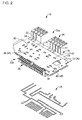
- FIGS. 1 to 6 show a circuit assembly 10 serving as an embodiment of the present invention.
- the circuit assembly 10 includes a printed circuit board 12 having printed wirings that are not shown, and a busbar circuit unit 16 that is constituted by a plurality of busbars 14.
- the circuit assembly 10 is constituted by the printed circuit board 12 on which electrical components 18 such as relays are mounted being overlapped with and fixed to the busbar circuit unit 16 via an adhesive sheet 20 from the upper side, and gaps 22 between busbars 14 being filled with an adhesive agent 24 from the lower side.
- “upper side” refers to the upper side of FIG. 1 in which the printed circuit board 12 is located
- lower side refers to the lower side of FIG. 1 in which the busbar circuit unit 16 is located.
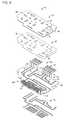
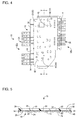
- the busbar circuit unit 16 has a configuration in which the plurality of busbars 14 are arranged adjacently and space apart by the gaps 22, and is formed by a conductive metal plate having a plated surface being pressed, punched, and bent by conventionally known means. Accordingly, as shown in FIG. 5 , a front surface 26 and a rear surface 28 of the busbars 14 maintain the state of being plated, whereas press-cut surfaces 30 (see FIG. 5 ) formed at both ends of each busbar 14 in the width direction are in the state of being unplated such that the plating of the surfaces is removed at the time of pressing and punching.
- the busbar circuit unit 16 has two ends 32a and 32b in its width direction, and at one end 32a (at the rear of FIG. 3 ), ends of the plurality of busbars 14 are bent in the shape of a crank and their tips are tuning fork-shaped, forming a fuse connection terminal section 34 into which connection sections of electrical components such as, for example, fuses that are not shown are inserted for connection.
- ends of the plurality of busbars 14 are similarly bent in the shape of a crank, forming a connector connection terminal section 36 that is to be inserted into, for example, a not-shown connector housing and serves as a connector terminal fitting.
- the printed circuit board 12 is overlapped with the busbar circuit unit 16 having such a configuration and is fixed thereto via the adhesive sheet 20 (see the upper part of FIG. 2 ). Specifically, a surface 40 of the printed circuit board 12 that is opposite to a mounting surface 38 on which the electrical components 18 are to be mounted, and the front surface 26 of the plurality of busbars 14 constituting the busbar circuit unit 16 are adhered to the adhesive sheet 20.
- the adhesive sheet 20 is formed so as to be slightly smaller than the busbar circuit unit 16, and has a plurality of through-holes 44 at positions that correspond to soldering sections 42 that are used for mounting terminal sections 50 of the electrical components 18 that will be described later.
- the adhesive sheet 20 is made of a resin sheet that has both surfaces applied with a well-known adhesive agent such as, for example, an epoxy resin.
- the printed circuit board 12 has substantially the same shape as that of the adhesive sheet 20, and has through-holes 46 at positions corresponding to the soldering sections 42 of the busbar circuit unit 16. Accordingly, the soldering sections 42 (see FIG. 4 ) for the busbars 14 are exposed on the mounting surface 38 of the printed circuit board 12 via the through-holes 44 and 46.
- the gaps 22 between the busbars 14 of the busbar circuit unit 16 to which the printed circuit board 12 is fixed in the above-described manner are filled with the adhesive agent 24.
- the gaps 22 between the busbars 14 are filled with a heat-resistant adhesive agent 24 of, for example, an UV (ultraviolet) curing type by a method such as screen printing.
- a heat-resistant adhesive agent 24 of, for example, an UV (ultraviolet) curing type by a method such as screen printing.
- UV (ultraviolet) irradiation device the rear surface 28 of the busbar circuit unit 16 is irradiated with UV (ultraviolet), and the adhesive agent 24 is cured. Accordingly, as shown in FIG. 5 , the press-cut surfaces 30 formed at the two ends of the busbars 14 in the width direction (horizontal direction of FIG.
- FIGS. 2 and 3 show the adhesive agent 24 after it is inserted into the gaps 22 between the busbars 14 and cured.
- the adhesive agent 24 of the UV (ultraviolet) curing type it is possible to immediately realize adhesion between the press-cut surfaces 30 of the busbars 14 and the adhesive sheet by the adhesive agent 24, achieving a reduction in working time. Furthermore, since curing is realized by emitting UV (ultraviolet), handling is easier than the case of a thermosetting adhesive agent that needs to be heated or a two-component adhesive agent in which curing is realized by a chemical reaction of a main agent and a curing agent, achieving simplification of the operation.
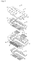
- the terminal sections 50 of the electrical components 18 are mounted to the printed wiring 48 of the printed circuit board 12 and the soldering section 42 of the busbar circuit unit 16 by reflow soldering using lead-free solder 52 or the like (see FIG. 6 ). Accordingly, since the electrical components 18 can easily be soldered to the printed wiring 48 of the printed circuit board 12 and the busbar 14 of the busbar circuit unit 16 by reflow soldering, the manufacturing process can be simplified.
- a tie-bar cutting process for cutting a tie-bar (not shown) that temporarily bundles the plurality of busbars 14, and a bending process for bending the ends of the busbars 14 to form the fuse connection terminal section 34 and the connector connection terminal section 36 are performed after the reflow soldering in the present embodiment, but may be performed before the reflow soldering. Note that for ease of understanding, in all the figures, the busbars 14 are shown in the state of having been completely subjected to the tie-bar cutting and the bending process.
- circuit assembly 10 of the present embodiment having such a configuration, even if when the electrical component 18 is soldered to the circuit assembly 10, the surface plating of the busbars 14 is melted and the adhesion between the front surface 26 of the busbars 14 and the adhesive sheet 20 is not maintained, adhesion between the busbars 14 and the adhesive sheet 20 by the adhesive agent 24 is maintained, and thus fixation between the busbar circuit unit 16 and the printed circuit board 12 can be held.
- the press-cut surfaces 30 of the busbars 14 to which the adhesive agent 24 is to be adhered are originally not plated, the adhesion between the press-cut surfaces 30 of the busbars 14 and the adhesive agent 24 is not affected by heating at the time of soldering. Furthermore, since the adhesive sheet 20 and the printed circuit board 12 to which the adhesive agent 24 is to be adhered are also not provided with plating that is to be melted when being heated at the time of soldering, the adhesion between the adhesive agent 24 and them is not affected by heating at the time of soldering. Therefore, it is possible to solve the problem that the busbar circuit unit 16 is removed from the printed circuit board 12 due to heating at the time of soldering.
- the adhesion between the press-cut surfaces 30 of the busbars 14 and the adhesive sheet 20 with the adhesive agent 24 is not affected by heating at the time of soldering, it is not necessary to change the type of the surface plating of the busbars 14 depending on the heating temperature at the time of soldering, improving the degree of freedom of selection for plating of the busbar 14.
- the busbars 14 can be plated with tin, which has a lower melting temperature than the lead-free solder 52.
- a circuit assembly 54 indicates an embodiment different from the above-described embodiment in that an adhesive sheet 56 has through-holes 58 that correspond to not only the soldering sections 42 of the busbar circuit unit 16 but also the gaps 22 between the busbars 14. Specifically, as shown in FIG.
- the printed circuit board 12 is exposed through the through-holes 58, and the press-cut surfaces 30 of the busbars 14 and the printed circuit board 12 are directly adhered to each other with the adhesive agent 24. Also in the circuit assembly 54 of the present embodiment, even if plating on the surfaces of the busbars 14 is melted, and the adhesion between the front surface 26 of the busbars 14 and the adhesive sheet 56 is not maintained, the busbars 14 and the printed circuit board 12 are adhered to each other with the adhesive agent 24, and thus the same effects as those of the circuit assembly 10 of the foregoing embodiment.
- the adhesive agent 24 can directly be fixed to the printed circuit board 12 that is harder than the adhesive sheet 56, it is possible to realize the fixation between the busbars 14 and the printed circuit board 12 by the adhesive agent 24 more reliably.
- any adhesive agent 24 may be used as long as it has a resistance against heating at the time of soldering, and a heat-resistant photo-curable adhesive agent of, for example, an UV curing type that is exemplified in the present embodiments, a thermosetting adhesive agent of an epoxy system, or the like is suitably used.
- the adhesive sheets 20 and 56 may be cohesive sheets such as highly heat-resistant double-faced tapes.
Landscapes
- Engineering & Computer Science (AREA)
- Microelectronics & Electronic Packaging (AREA)
- Coupling Device And Connection With Printed Circuit (AREA)
- Connection Or Junction Boxes (AREA)
- Electric Connection Of Electric Components To Printed Circuits (AREA)
Applications Claiming Priority (2)
| Application Number | Priority Date | Filing Date | Title |
|---|---|---|---|
| JP2013196765A JP5958768B2 (ja) | 2013-09-24 | 2013-09-24 | 回路構成体 |
| PCT/JP2014/073242 WO2015045768A1 (ja) | 2013-09-24 | 2014-09-03 | 回路構成体 |
Publications (2)
| Publication Number | Publication Date |
|---|---|
| EP3051641A1 true EP3051641A1 (de) | 2016-08-03 |
| EP3051641A4 EP3051641A4 (de) | 2016-10-12 |
Family
ID=52742915
Family Applications (1)
| Application Number | Title | Priority Date | Filing Date |
|---|---|---|---|
| EP14848339.9A Withdrawn EP3051641A4 (de) | 2013-09-24 | 2014-09-03 | Schaltungsanordnung |
Country Status (5)
| Country | Link |
|---|---|
| US (1) | US9635754B2 (de) |
| EP (1) | EP3051641A4 (de) |
| JP (1) | JP5958768B2 (de) |
| CN (1) | CN105580226B (de) |
| WO (1) | WO2015045768A1 (de) |
Families Citing this family (5)
| Publication number | Priority date | Publication date | Assignee | Title |
|---|---|---|---|---|
| JP6593597B2 (ja) * | 2016-03-16 | 2019-10-23 | 株式会社オートネットワーク技術研究所 | 回路構成体 |
| JP6667105B2 (ja) * | 2016-04-15 | 2020-03-18 | 株式会社オートネットワーク技術研究所 | 回路基板、回路構成体、及び回路基板の製造方法 |
| KR101989859B1 (ko) * | 2016-12-15 | 2019-09-30 | 주식회사 아모그린텍 | 파워 릴레이 어셈블리 |
| JP6988729B2 (ja) * | 2018-07-31 | 2022-01-05 | 株式会社オートネットワーク技術研究所 | 電気接続箱 |
| JP7677118B2 (ja) * | 2021-10-29 | 2025-05-15 | 住友電装株式会社 | 回路構成体 |
Family Cites Families (13)
| Publication number | Priority date | Publication date | Assignee | Title |
|---|---|---|---|---|
| JPH0759130B2 (ja) | 1991-10-18 | 1995-06-21 | 矢崎総業株式会社 | 電気接続箱の防水シール方法 |
| JPH07336843A (ja) * | 1994-06-09 | 1995-12-22 | Yazaki Corp | 電気接続箱 |
| JP3927017B2 (ja) * | 2001-11-26 | 2007-06-06 | 株式会社オートネットワーク技術研究所 | 回路構成体及びその製造方法 |
| DE10254910B4 (de) | 2001-11-26 | 2008-12-24 | AutoNetworks Technologies, Ltd., Nagoya | Schaltkreisbildende Einheit und Verfahren zu deren Herstellung |
| JP4022440B2 (ja) * | 2002-07-01 | 2007-12-19 | 株式会社オートネットワーク技術研究所 | 回路ユニット |
| JP4059097B2 (ja) * | 2003-02-14 | 2008-03-12 | 住友電装株式会社 | 回路構成体 |
| JP2006005096A (ja) * | 2004-06-16 | 2006-01-05 | Auto Network Gijutsu Kenkyusho:Kk | 回路構成体 |
| JP2006203977A (ja) | 2005-01-18 | 2006-08-03 | Sumitomo Wiring Syst Ltd | 電気接続箱 |
| JP4594198B2 (ja) * | 2005-09-02 | 2010-12-08 | 株式会社オートネットワーク技術研究所 | 電気接続箱 |
| JP4585980B2 (ja) | 2005-10-14 | 2010-11-24 | 株式会社オートネットワーク技術研究所 | 電気接続箱 |
| JP4582717B2 (ja) * | 2006-05-09 | 2010-11-17 | 株式会社オートネットワーク技術研究所 | 回路構成体 |
| US20080160754A1 (en) * | 2006-12-27 | 2008-07-03 | International Business Machines Corporation | Method for fabricating a microelectronic conductor structure |
| EP2533616A4 (de) * | 2010-02-01 | 2016-08-10 | Furukawa Electric Co Ltd | Metallkernsubstrat für einen fahrzeuginternen elektrischen verbindungskasten |
-
2013
- 2013-09-24 JP JP2013196765A patent/JP5958768B2/ja not_active Expired - Fee Related
-
2014
- 2014-09-03 CN CN201480052540.2A patent/CN105580226B/zh not_active Expired - Fee Related
- 2014-09-03 WO PCT/JP2014/073242 patent/WO2015045768A1/ja not_active Ceased
- 2014-09-03 EP EP14848339.9A patent/EP3051641A4/de not_active Withdrawn
- 2014-09-03 US US15/024,395 patent/US9635754B2/en not_active Expired - Fee Related
Also Published As
| Publication number | Publication date |
|---|---|
| JP2015065722A (ja) | 2015-04-09 |
| CN105580226B (zh) | 2018-02-23 |
| EP3051641A4 (de) | 2016-10-12 |
| WO2015045768A1 (ja) | 2015-04-02 |
| US20160242275A1 (en) | 2016-08-18 |
| JP5958768B2 (ja) | 2016-08-02 |
| CN105580226A (zh) | 2016-05-11 |
| US9635754B2 (en) | 2017-04-25 |
Similar Documents
| Publication | Publication Date | Title |
|---|---|---|
| EP3051642A1 (de) | Schaltungsanordnung | |
| US9635754B2 (en) | Circuit assembly | |
| US10576912B2 (en) | Circuit assembly and electrical junction box | |
| EP2355259B1 (de) | Elektrischer Verteilerkasten | |
| KR102629256B1 (ko) | 보호 소자 | |
| EP2568539B1 (de) | Leiterverbindungswerkzeug und Relaiseinheit damit | |
| CN108028520B (zh) | 电路结构体及电连接箱 | |
| KR20210114538A (ko) | 보호 소자 | |
| KR101683386B1 (ko) | 이중 두께 이중-단부형 수형 블레이드 단자 | |
| WO2015174263A1 (ja) | 回路構成体および電気接続箱 | |
| JP2008054449A (ja) | 電気接続箱に収容する回路材 | |
| CN118947020A (zh) | 配线模块 | |
| EP3624152B1 (de) | Bürstenschalter mit widerständen und herstellungsverfahren dafür | |
| JP6899246B2 (ja) | 電子部品 | |
| EP2825003B1 (de) | Leiterplatte und Elektrowerkzeugschalter damit | |
| JP2015220188A (ja) | 端子、端子固定構造及び回路遮断器 | |
| US9991068B2 (en) | Push-button switch | |
| JP2006514436A (ja) | フラットケーブルに部品を電気的に接触させる方法 | |
| JP2008092726A (ja) | 回路材および回路材の形成方法 | |
| CN118975029A (zh) | 配线模块 | |
| JP2009016694A (ja) | プリント基板およびその製造方法 | |
| JP2016154078A (ja) | ハウジングレスヒューズ | |
| JP2005322568A (ja) | 端子の接続方法及び回路基板 | |
| JP2015056475A (ja) | 電気装置 | |
| KR20170136602A (ko) | 어셈블리 |
Legal Events
| Date | Code | Title | Description |
|---|---|---|---|
| PUAI | Public reference made under article 153(3) epc to a published international application that has entered the european phase |
Free format text: ORIGINAL CODE: 0009012 |
|
| 17P | Request for examination filed |
Effective date: 20160310 |
|
| AK | Designated contracting states |
Kind code of ref document: A1 Designated state(s): AL AT BE BG CH CY CZ DE DK EE ES FI FR GB GR HR HU IE IS IT LI LT LU LV MC MK MT NL NO PL PT RO RS SE SI SK SM TR |
|
| AX | Request for extension of the european patent |
Extension state: BA ME |
|
| A4 | Supplementary search report drawn up and despatched |
Effective date: 20160909 |
|
| RIC1 | Information provided on ipc code assigned before grant |
Ipc: H05K 3/38 20060101ALI20160905BHEP Ipc: H05K 1/02 20060101ALI20160905BHEP Ipc: H02G 3/16 20060101AFI20160905BHEP Ipc: H05K 7/06 20060101ALI20160905BHEP |
|
| DAX | Request for extension of the european patent (deleted) | ||
| STAA | Information on the status of an ep patent application or granted ep patent |
Free format text: STATUS: EXAMINATION IS IN PROGRESS |
|
| 17Q | First examination report despatched |
Effective date: 20200708 |
|
| GRAP | Despatch of communication of intention to grant a patent |
Free format text: ORIGINAL CODE: EPIDOSNIGR1 |
|
| STAA | Information on the status of an ep patent application or granted ep patent |
Free format text: STATUS: GRANT OF PATENT IS INTENDED |
|
| INTG | Intention to grant announced |
Effective date: 20220504 |
|
| STAA | Information on the status of an ep patent application or granted ep patent |
Free format text: STATUS: THE APPLICATION IS DEEMED TO BE WITHDRAWN |
|
| 18D | Application deemed to be withdrawn |
Effective date: 20220915 |