EP3043340B1 - Display device and method for controlling brightness thereof - Google Patents
Display device and method for controlling brightness thereof Download PDFInfo
- Publication number
- EP3043340B1 EP3043340B1 EP13892154.9A EP13892154A EP3043340B1 EP 3043340 B1 EP3043340 B1 EP 3043340B1 EP 13892154 A EP13892154 A EP 13892154A EP 3043340 B1 EP3043340 B1 EP 3043340B1
- Authority
- EP
- European Patent Office
- Prior art keywords
- luminance
- apl
- weight value
- data
- image
- Prior art date
- Legal status (The legal status is an assumption and is not a legal conclusion. Google has not performed a legal analysis and makes no representation as to the accuracy of the status listed.)
- Active
Links
- 238000000034 method Methods 0.000 title claims description 18
- 230000002093 peripheral effect Effects 0.000 claims description 15
- 230000008859 change Effects 0.000 claims description 12
- 230000004044 response Effects 0.000 claims description 7
- 235000019557 luminance Nutrition 0.000 description 257
- 239000010410 layer Substances 0.000 description 12
- 239000004973 liquid crystal related substance Substances 0.000 description 8
- 238000010586 diagram Methods 0.000 description 6
- 238000004891 communication Methods 0.000 description 5
- 230000009467 reduction Effects 0.000 description 5
- 238000002347 injection Methods 0.000 description 4
- 239000007924 injection Substances 0.000 description 4
- 239000011159 matrix material Substances 0.000 description 4
- 238000012986 modification Methods 0.000 description 3
- 230000004048 modification Effects 0.000 description 3
- 229920001621 AMOLED Polymers 0.000 description 2
- 208000036762 Acute promyelocytic leukaemia Diseases 0.000 description 2
- 239000003990 capacitor Substances 0.000 description 2
- 239000003086 colorant Substances 0.000 description 2
- 238000005516 engineering process Methods 0.000 description 2
- 230000006870 function Effects 0.000 description 2
- 230000005525 hole transport Effects 0.000 description 2
- 238000004519 manufacturing process Methods 0.000 description 2
- 150000002894 organic compounds Chemical class 0.000 description 2
- 230000008569 process Effects 0.000 description 2
- 230000003068 static effect Effects 0.000 description 2
- 238000003860 storage Methods 0.000 description 2
- 239000010409 thin film Substances 0.000 description 2
- 230000001133 acceleration Effects 0.000 description 1
- 238000004458 analytical method Methods 0.000 description 1
- 238000006243 chemical reaction Methods 0.000 description 1
- 238000011161 development Methods 0.000 description 1
- 230000005684 electric field Effects 0.000 description 1
- 238000001962 electrophoresis Methods 0.000 description 1
- 230000004313 glare Effects 0.000 description 1
- 230000005484 gravity Effects 0.000 description 1
- 230000006872 improvement Effects 0.000 description 1
- 230000005389 magnetism Effects 0.000 description 1
- 239000000463 material Substances 0.000 description 1
- 238000005457 optimization Methods 0.000 description 1
- 239000012044 organic layer Substances 0.000 description 1
- 230000001360 synchronised effect Effects 0.000 description 1
- 238000012360 testing method Methods 0.000 description 1
- 230000007704 transition Effects 0.000 description 1
Images


Classifications
-
- G—PHYSICS
- G09—EDUCATION; CRYPTOGRAPHY; DISPLAY; ADVERTISING; SEALS
- G09G—ARRANGEMENTS OR CIRCUITS FOR CONTROL OF INDICATING DEVICES USING STATIC MEANS TO PRESENT VARIABLE INFORMATION
- G09G5/00—Control arrangements or circuits for visual indicators common to cathode-ray tube indicators and other visual indicators
- G09G5/10—Intensity circuits
-
- G—PHYSICS
- G09—EDUCATION; CRYPTOGRAPHY; DISPLAY; ADVERTISING; SEALS
- G09G—ARRANGEMENTS OR CIRCUITS FOR CONTROL OF INDICATING DEVICES USING STATIC MEANS TO PRESENT VARIABLE INFORMATION
- G09G3/00—Control arrangements or circuits, of interest only in connection with visual indicators other than cathode-ray tubes
- G09G3/20—Control arrangements or circuits, of interest only in connection with visual indicators other than cathode-ray tubes for presentation of an assembly of a number of characters, e.g. a page, by composing the assembly by combination of individual elements arranged in a matrix no fixed position being assigned to or needed to be assigned to the individual characters or partial characters
- G09G3/34—Control arrangements or circuits, of interest only in connection with visual indicators other than cathode-ray tubes for presentation of an assembly of a number of characters, e.g. a page, by composing the assembly by combination of individual elements arranged in a matrix no fixed position being assigned to or needed to be assigned to the individual characters or partial characters by control of light from an independent source
- G09G3/36—Control arrangements or circuits, of interest only in connection with visual indicators other than cathode-ray tubes for presentation of an assembly of a number of characters, e.g. a page, by composing the assembly by combination of individual elements arranged in a matrix no fixed position being assigned to or needed to be assigned to the individual characters or partial characters by control of light from an independent source using liquid crystals
- G09G3/3611—Control of matrices with row and column drivers
- G09G3/3648—Control of matrices with row and column drivers using an active matrix
-
- G—PHYSICS
- G09—EDUCATION; CRYPTOGRAPHY; DISPLAY; ADVERTISING; SEALS
- G09G—ARRANGEMENTS OR CIRCUITS FOR CONTROL OF INDICATING DEVICES USING STATIC MEANS TO PRESENT VARIABLE INFORMATION
- G09G3/00—Control arrangements or circuits, of interest only in connection with visual indicators other than cathode-ray tubes
- G09G3/20—Control arrangements or circuits, of interest only in connection with visual indicators other than cathode-ray tubes for presentation of an assembly of a number of characters, e.g. a page, by composing the assembly by combination of individual elements arranged in a matrix no fixed position being assigned to or needed to be assigned to the individual characters or partial characters
- G09G3/22—Control arrangements or circuits, of interest only in connection with visual indicators other than cathode-ray tubes for presentation of an assembly of a number of characters, e.g. a page, by composing the assembly by combination of individual elements arranged in a matrix no fixed position being assigned to or needed to be assigned to the individual characters or partial characters using controlled light sources
- G09G3/30—Control arrangements or circuits, of interest only in connection with visual indicators other than cathode-ray tubes for presentation of an assembly of a number of characters, e.g. a page, by composing the assembly by combination of individual elements arranged in a matrix no fixed position being assigned to or needed to be assigned to the individual characters or partial characters using controlled light sources using electroluminescent panels
- G09G3/32—Control arrangements or circuits, of interest only in connection with visual indicators other than cathode-ray tubes for presentation of an assembly of a number of characters, e.g. a page, by composing the assembly by combination of individual elements arranged in a matrix no fixed position being assigned to or needed to be assigned to the individual characters or partial characters using controlled light sources using electroluminescent panels semiconductive, e.g. using light-emitting diodes [LED]
- G09G3/3208—Control arrangements or circuits, of interest only in connection with visual indicators other than cathode-ray tubes for presentation of an assembly of a number of characters, e.g. a page, by composing the assembly by combination of individual elements arranged in a matrix no fixed position being assigned to or needed to be assigned to the individual characters or partial characters using controlled light sources using electroluminescent panels semiconductive, e.g. using light-emitting diodes [LED] organic, e.g. using organic light-emitting diodes [OLED]
- G09G3/3225—Control arrangements or circuits, of interest only in connection with visual indicators other than cathode-ray tubes for presentation of an assembly of a number of characters, e.g. a page, by composing the assembly by combination of individual elements arranged in a matrix no fixed position being assigned to or needed to be assigned to the individual characters or partial characters using controlled light sources using electroluminescent panels semiconductive, e.g. using light-emitting diodes [LED] organic, e.g. using organic light-emitting diodes [OLED] using an active matrix
- G09G3/3233—Control arrangements or circuits, of interest only in connection with visual indicators other than cathode-ray tubes for presentation of an assembly of a number of characters, e.g. a page, by composing the assembly by combination of individual elements arranged in a matrix no fixed position being assigned to or needed to be assigned to the individual characters or partial characters using controlled light sources using electroluminescent panels semiconductive, e.g. using light-emitting diodes [LED] organic, e.g. using organic light-emitting diodes [OLED] using an active matrix with pixel circuitry controlling the current through the light-emitting element
-
- G—PHYSICS
- G09—EDUCATION; CRYPTOGRAPHY; DISPLAY; ADVERTISING; SEALS
- G09G—ARRANGEMENTS OR CIRCUITS FOR CONTROL OF INDICATING DEVICES USING STATIC MEANS TO PRESENT VARIABLE INFORMATION
- G09G2300/00—Aspects of the constitution of display devices
- G09G2300/08—Active matrix structure, i.e. with use of active elements, inclusive of non-linear two terminal elements, in the pixels together with light emitting or modulating elements
- G09G2300/0809—Several active elements per pixel in active matrix panels
- G09G2300/0842—Several active elements per pixel in active matrix panels forming a memory circuit, e.g. a dynamic memory with one capacitor
-
- G—PHYSICS
- G09—EDUCATION; CRYPTOGRAPHY; DISPLAY; ADVERTISING; SEALS
- G09G—ARRANGEMENTS OR CIRCUITS FOR CONTROL OF INDICATING DEVICES USING STATIC MEANS TO PRESENT VARIABLE INFORMATION
- G09G2320/00—Control of display operating conditions
- G09G2320/02—Improving the quality of display appearance
- G09G2320/0242—Compensation of deficiencies in the appearance of colours
-
- G—PHYSICS
- G09—EDUCATION; CRYPTOGRAPHY; DISPLAY; ADVERTISING; SEALS
- G09G—ARRANGEMENTS OR CIRCUITS FOR CONTROL OF INDICATING DEVICES USING STATIC MEANS TO PRESENT VARIABLE INFORMATION
- G09G2320/00—Control of display operating conditions
- G09G2320/02—Improving the quality of display appearance
- G09G2320/0261—Improving the quality of display appearance in the context of movement of objects on the screen or movement of the observer relative to the screen
-
- G—PHYSICS
- G09—EDUCATION; CRYPTOGRAPHY; DISPLAY; ADVERTISING; SEALS
- G09G—ARRANGEMENTS OR CIRCUITS FOR CONTROL OF INDICATING DEVICES USING STATIC MEANS TO PRESENT VARIABLE INFORMATION
- G09G2320/00—Control of display operating conditions
- G09G2320/06—Adjustment of display parameters
- G09G2320/0606—Manual adjustment
-
- G—PHYSICS
- G09—EDUCATION; CRYPTOGRAPHY; DISPLAY; ADVERTISING; SEALS
- G09G—ARRANGEMENTS OR CIRCUITS FOR CONTROL OF INDICATING DEVICES USING STATIC MEANS TO PRESENT VARIABLE INFORMATION
- G09G2320/00—Control of display operating conditions
- G09G2320/06—Adjustment of display parameters
- G09G2320/0626—Adjustment of display parameters for control of overall brightness
-
- G—PHYSICS
- G09—EDUCATION; CRYPTOGRAPHY; DISPLAY; ADVERTISING; SEALS
- G09G—ARRANGEMENTS OR CIRCUITS FOR CONTROL OF INDICATING DEVICES USING STATIC MEANS TO PRESENT VARIABLE INFORMATION
- G09G2320/00—Control of display operating conditions
- G09G2320/06—Adjustment of display parameters
- G09G2320/0666—Adjustment of display parameters for control of colour parameters, e.g. colour temperature
-
- G—PHYSICS
- G09—EDUCATION; CRYPTOGRAPHY; DISPLAY; ADVERTISING; SEALS
- G09G—ARRANGEMENTS OR CIRCUITS FOR CONTROL OF INDICATING DEVICES USING STATIC MEANS TO PRESENT VARIABLE INFORMATION
- G09G2330/00—Aspects of power supply; Aspects of display protection and defect management
- G09G2330/02—Details of power systems and of start or stop of display operation
- G09G2330/021—Power management, e.g. power saving
-
- G—PHYSICS
- G09—EDUCATION; CRYPTOGRAPHY; DISPLAY; ADVERTISING; SEALS
- G09G—ARRANGEMENTS OR CIRCUITS FOR CONTROL OF INDICATING DEVICES USING STATIC MEANS TO PRESENT VARIABLE INFORMATION
- G09G2354/00—Aspects of interface with display user
-
- G—PHYSICS
- G09—EDUCATION; CRYPTOGRAPHY; DISPLAY; ADVERTISING; SEALS
- G09G—ARRANGEMENTS OR CIRCUITS FOR CONTROL OF INDICATING DEVICES USING STATIC MEANS TO PRESENT VARIABLE INFORMATION
- G09G2360/00—Aspects of the architecture of display systems
- G09G2360/14—Detecting light within display terminals, e.g. using a single or a plurality of photosensors
- G09G2360/144—Detecting light within display terminals, e.g. using a single or a plurality of photosensors the light being ambient light
-
- G—PHYSICS
- G09—EDUCATION; CRYPTOGRAPHY; DISPLAY; ADVERTISING; SEALS
- G09G—ARRANGEMENTS OR CIRCUITS FOR CONTROL OF INDICATING DEVICES USING STATIC MEANS TO PRESENT VARIABLE INFORMATION
- G09G2360/00—Aspects of the architecture of display systems
- G09G2360/16—Calculation or use of calculated indices related to luminance levels in display data
Definitions
- Embodiments of the invention relate to a display device and a method for controlling a luminance of the display device.
- Examples of a flat panel display include a liquid crystal display (LCD), a plasma display panel (PDP), an organic light emitting display, and an electrophoresis display (EPD).
- the liquid crystal display displays an image by controlling an electric field applied to liquid crystal molecules based on a data voltage.
- An active matrix liquid crystal display has advantages of a reduction in the production cost and an improvement of a performance with the development of the process technology and the driving technology.
- the active matrix liquid crystal display is the most widely used display device applied to almost all display devices including small mobile equipments and large-sized televisions.
- the organic light emitting display is a self-emitting device, it has advantages of lower power consumption and thinner profile than the liquid crystal display requiring a backlight unit. Further, the organic light emitting display has advantages of a wide viewing angle and a fast response time. Thus, the organic light emitting display has expanded its market while competing with the liquid crystal display.
- Each pixel of the organic light emitting display includes an organic light emitting diode (OLED) having a self-emitting structure.
- the OLED includes organic compound layers, such as a hole injection layer HIL, a hole transport layer HTL, an emission layer EML, an electron transport layer ETL, and an electron injection layer EIL, which are stacked between an anode and a cathode.
- the organic light emitting display reproduces an input image using a phenomenon in which the OLED emits light when electrons and holes are combined in an organic layer of the OLED through a current flowing in a fluorescence or phosphorescence organic thin film.
- the organic light emitting display may be variously classified depending on a light emitting material, a light emitting manner, a light emitting structure, a driving method, etc.
- the organic light emitting display may be classified into a fluorescence emission type and a phosphorescence emission type depending on the light emitting manner, and may be classified into a top emission type and a bottom top emission type depending on the light emitting structure. Further, the organic light emitting display may be classified into a passive matrix OLED (PMOLED) type and an active matrix OLED (AMOLED) type depending on the driving method.
- PMOLED passive matrix OLED
- AMOLED active matrix OLED
- US 2011/0205442 A1 discloses a display device configured to adjust a gain of a video signal to permit control of average and peak brightness of a video frame, and thereby power consumption of the display device.
- the display device includes a table calculating unit that calculates a table representing a relationship between an average brightness and a gain of a video signal, and a table revision unit that revises the table in order to reduce a change amount of a gain in each frame in the table.
- a current-brightness control table then calculates a gain of a video signal from the table based on the average brightness of the video signal calculated by a video-average brightness conversion block.
- CN 101 102 437 A discloses a brightness adjusting method of a backlight of a liquid crystal display.
- a table is created and stored defining a relationship between an average picture level (APL) and a relative peak luminance.
- APL average picture level
- The, the relative peak brightness of a video signal is calculated and the corresponding relative peak luminance is derived from the stored table.
- the backlight brightness is adjusted.
- KR 2010 0052833 A discloses another method and apparatus for controlling power consumption of an image display device.
- CN103035193 discloses a plasma display device adopting different APL curves for dynamic and static images, configured to spare power consumption by reducing a number of sustain pulses for displaying dynamic images, along with guaranteeing a smooth brightness transition between static and dynamic images.
- the power consumption may be reduced through a simple method for reducing the luminance of the screen, but the image quality may be degraded.
- Embodiments of the invention are set out in the appended claims and provide a display device and a method for controlling a luminance of the display device capable of minimizing a reduction in image quality and reducing power consumption.
- the display device comprises an average picture level (APL) calculator configured to calculate an APL of an input image and output the APL of the input image and an APL curve data, a luminance adjuster including at least two luminance adjusting units, which are enabled in response to a user input through a user interface, the luminance adjuster adjusting the APL curve data, a data modulator configured to modulate data of the input image using a luminance defined in the APL curve data adjusted by the luminance adjuster, and a display panel driving circuit configured to write data from the data modulator on a display panel and reproduce the input image on the display panel.
- APL average picture level
- an organic light emitting display includes a display panel 10, a display panel driving circuit, a timing controller 11, a host system 100, etc.
- the display panel 10 includes a plurality of data lines 14 and a plurality of gate lines 15 crossing the data lines 14.
- a pixel array of the display panel 10 includes pixels P which are disposed in a matrix form and display an input image.
- each pixel P includes an organic light emitting diode (OLED), a switching element SWTFT, a driving element DRTFT, a storage capacitor Cst, etc.
- the switching element SWTFT and the driving element DRTFT may be implemented as a thin film transistor (TFT). As shown in FIG.
- the OLED may include organic compound layers, such as a hole injection layer HIL, a hole transport layer HTL, an emission layer EML, an electron transport layer ETL, and an electron injection layer EIL, which are stacked between an anode and a cathode.
- the switching element SWTFT applies a data voltage input through the data line 14 to a gate of the driving element DRTFT in response to a gate pulse.
- a gate of the switching element SWTFT is connected to the gate line 15.
- a drain of the switching element SWTFT is connected to the data line 14, and a source of the switching element SWTFT is connected to the gate of the driving element DRTFT.
- the driving element DRTFT adjusts a current flowing in the OLED depending on a gate voltage.
- a high potential power voltage VDD for driving the pixel is applied to a drain of the driving element DRTFT.
- a source of the driving element DRTFT is connected to the anode of the OLED.
- the storage capacitor Cst is connected between the gate and the drain of the driving element DRTFT.
- the anode of the OLED is connected to the source of the driving element DRTFT, and the cathode of the OLED is connected to a ground level voltage source GND.
- Each pixel P may additionally include an internal compensation circuit (not shown). The internal compensation circuit compensates for changes in a threshold voltage and a mobility of the driving element DRTFT
- the display panel driving circuit includes a data driving circuit 12 and a gate driving circuit 13.
- the display panel driving circuit writes data of the input image modulated by the timing controller 11 on the display panel 10 and reproduces the input image on the display panel 10.
- the data driving circuit 12 includes at least one source driver integrated circuit (IC).
- the data driving circuit 12 converts pixel data DATA of the input image received from the timing controller 11 into analog gamma compensation voltage and generates the data voltage.
- the data driving circuit 12 outputs the data voltage to the data lines 14.
- the pixel data DATA input to the data driving circuit 12 is digital video data of the input image.
- Each pixel data DATA includes red data, green data, and blue data.
- the gate driving circuit 13 supplies a gate pulse (or a scan pulse) synchronized with an output voltage of the data driving circuit 12 to the gate lines 15 under the control of the timing controller 11.
- the gate driving circuit 13 sequentially shifts the gate pulse and sequentially selects the pixels P, on which the data is written, on a per line basis.
- the host system 100 may be implemented as one of a television system, a set-top box, a navigation system, a DVD player, a Blu-ray player, a personal computer (PC), a home theater system, and a phone system.
- the host system 100 calculates an average picture level (hereinafter referred to as "APL") in each frame of the input image.
- the host system 100 performs at least one luminance adjusting unit selected depending on a user input through a user interface (UI) 110 and adjusts an APL curve.
- the host system 100 produces data APL' of the APL curve and transmits the APL curve data APL' to the timing controller 11.
- the APL curve data APL' may be 8-bit data.
- the APL curve data APL' output from the host system 100 may be transmitted to the timing controller 11 in a vertical blank period of each frame period.
- the vertical blank period is a period between an Nth frame period and an (N+1)th frame period, where N is a positive integer. There is no data in the vertical blank period.
- the timing controller 11 receives the pixel data DATA of the input image, the APL curve data APL', and timing signals from the host system 100.
- the timing controller 11 modulates gray levels of the pixel data DATA, so that a luminance of the input image is limited to a luminance equal to or less than a maximum luminance defined in the APL curve data APL'. Further, the timing controller 11 generates timing control signals DDC and GDC for controlling operation timings of the data driving circuit 12 and the gate driving circuit 13 based on the timing signals received along with the pixel data DATA of the input image.
- the timing signals input to the timing controller 11 include a vertical sync signal Vsync, a horizontal sync signal Hsync, a data enable signal DE, and a main clock CLK, etc.
- the timing controller 11 modulates the pixel data DATA of the input image based on a luminance defined in the APL curve data APL' received from the host system 100 using a data modulator 20 and transmits the modulated pixel data DATA to the data driving circuit 12.
- the data modulator 20 may be implemented as a lookup table LUT.
- the data modulator 20 modulates the pixel data DATA of the input image and may adjust a luminance or a color temperature of a display image displayed on the display panel 10.
- the lookup table LUT receives the APL curve data APL' and the pixel data DATA of the input image and outputs a modulation value previously stored in an address which the input data indicates, thereby modulating the gray levels of the pixel data DATA.
- the modulation value of the lookup table LUT is individually set based on each APL curve data APL' and also is individually set based on each gray level of the pixel data DATA. Hence, the luminance of the pixel data DATA is set to be equal to or less than the maximum luminance defined in the APL curve data APL'.
- the user interface 110 may be implemented as a keypad, a keyboard, a mouse, an on-screen display (OSD), a remote controller having an infrared communication function or a radio frequency (RF) communication function, a touch UI, a voice recognition UI, a 3D UI, etc.
- OSD on-screen display
- RF radio frequency
- the host system 100 may be connected to a sensing unit 120.
- the sensing unit 120 includes an image sensor (or a camera), an illuminance sensor, a color temperature sensor, a microphone, an acceleration sensor, a gravity sensor, a proximity sensor, a terrestrial magnetism sensor, a gyroscope angular velocity sensor, etc.
- the sensing unit 120 converts the outputs of these sensors into digital data and supplies the digital data to the host system 100.
- the color temperature sensor senses a color temperature using a red light sensor, a green light sensor, and a blue light sensor.
- the host system 100 may control the luminances of the pixels in response to the outputs of the sensors.
- the host system 100 analyzes the output of the illuminance sensor and decides an illuminance of a surrounding environment of the display device.
- the host system 100 may adjust the APL curve depending on the illuminance of the surrounding environment.
- the host system 100 adjusts a white balance value of the pixel depending on a color temperature of the surrounding environment and may adjust a color temperature of the display image.
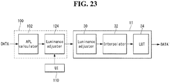
- FIG. 4 is a block diagram of a graphic controller of the host system 100.
- FIG. 5 is a block diagram showing in detail a luminance adjuster shown in FIG. 4 .
- FIGs. 6 to 8 show various examples of a method for adjusting a luminance.
- a graphic controller of the host system 100 includes an APL calculator 102, a luminance adjuster 104, an interpolator 106, an APL curve data transmitter 108, etc.
- the APL calculator 102 calculates the APL in each frame of the input image.
- the APL is an average luminance value of pixel data corresponding to one frame. In general, the high APL indicates a bright image, and the low APL indicates a dark image.
- the APL calculator 102 receives the APL curve data APL' from the timing controller 11 and supplies the APL curve data and the APL of the input image to the luminance adjuster 104. There may be a deviation in luminance, current, and driving characteristics of the display panel 10.
- the characteristic information of the display panel 10 is embedded in the timing controller 11.
- the APL curve data considering the characteristic deviation of the display panel 10 may be stored in the timing controller 11.
- the APL calculator 102 may not receive the APL curve data from the timing controller 11 and may transmit the APL curve data APL' previously stored in a built-in memory to the luminance adjuster 104.
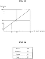
- the APL curve data transmitted to the luminance adjuster 104 may include only N APL points p0 to p7 on the APL curve shown in FIG. 9 , so as to reduce an operation amount of data, where N is a positive integer between 2 and 20.
- the N APL points p0 to p7 are points positioned at boundaries between neighboring sections when the APL curve is equally divided into N sections. In the APL curve shown in FIGs. 9 and 10 , N is 8, for example.
- the luminance adjuster 104 performs at least one luminance adjusting unit selected based on user input data input through the user interface 110 and adjusts the APL curve. According to the APL curve shown in FIGs. 9 and 10 , the maximum luminance of the display image increases when the APL is reduced, and the maximum luminance of the display image is reduced when the APL increases.
- the timing controller 11 reduces the luminance of the display device based on the APL curve and may reduce the current flowing in the OLED of the pixel.
- the luminance adjuster 104 adjusts the APL curve data received from the APL calculator 102 and outputs the APL curve data APL' shown in FIG. 10 .
- the APL curve defines the maximum luminance depending on the APL of the input image. According to the APL curve, when the APL of the input image is reduced, the maximum luminance of the display image increases. Further, when the APL of the input image increases, the maximum luminance of the display image is reduced.
- the host system 100 adjusts the APL curve using the luminance adjuster 104, thereby minimizing a reduction in the image quality. Further, the host system 100 may control power consumption at a level equal to or less than a predetermined level even if an average luminance of the input image changes.
- the interpolator 106 calculates a luminance between luminances corresponding to the neighboring APL points p0 to p7 through a linear interpolation method. As a result, the interpolator 106 produces luminance data connecting the luminances corresponding to the neighboring APL points p0 to p7 and outputs the APL curve data APL' defining the maximum luminance of the display image on the entire APL curve.
- the APL curve data transmitter 108 transmits the APL curve data APL' received from the interpolator 106 to the timing controller 11.
- the data modulator 20 of the timing controller 11 modulates the pixel data of the input image based on the maximum luminance defined in the APL curve data APL' and thus may adjust the luminance or the color temperature of the display image.
- the data modulator 20 may be implemented as the lookup table LUT.
- the luminance adjuster 104 may output the APL curve data defining the maximum luminance with respect to all of the APLs.
- the interpolator 106 may be omitted, and the APL curve data output from the luminance adjuster 104 may be transmitted to the timing controller 11.
- the luminance adjuster 104 includes first to fifth luminance adjusting units 50, 52, 54, 56, and 58 and first to fifth multipliers 51, 53, 55, 57, and 59.
- the first to fifth luminance adjusting units 50, 52, 54, 56, and 58 may be enabled to operate or disabled depending on the input of the user interface 110.
- the input of the user interface 110 may be maker input data input by a set maker manufacturing the display device and may be user input data using the display device.
- the first luminance adjusting unit 50 receives the input of the user interface 110 and adjusts the luminance of the display image. As shown in FIGs. 12 and 13 , the first luminance adjusting unit 50 sets a first weight value ⁇ 1 in response to an UI input luminance input through the user interface 110 and adjusts the luminance of the display image. In this instance, when the UI input luminance is zero, the maximum luminance of the display image is limited to a value greater than zero. This is because a minimum luminance of the display image controlled by the third luminance adjusting unit 54 is greatly reduced when the first luminance adjusting unit 50 greatly reduces the maximum luminance of the display image.
- the first weight value ⁇ 1 is set to be greater than zero and equal to or less than 1.
- the first multiplier 51 adjusts the luminances of the APL points p0 to p7 by multiplying the luminance of each of the APL points p0 to p7 by the first weight value ⁇ 1.
- a picture sound mode PSM may be set in the host system 100.
- the first luminance adjusting unit 50 may adjust the maximum luminance of the display image based on the picture sound mode PSM.
- the picture sound mode PSM defines various image modes, which the user can select, in consideration of a viewing environment and viewing conditions of the user using the display device.
- the picture sound mode PSM may include a vivid mode, a standard mode, an eco mode, a cinema mode, a game mode, an expert mode, etc. which the user can select through the user interface 110.
- the user may select the image modes defined in the picture sound mode PSM through the user interface 110.
- the various image modes are described below.
- the vivid mode is an image mode, in which the image quality is improved to the maximum so as to show a bright and vivid image in a store.
- the standard mode is a standard image mode, in which the user can comfortably use at the home.
- the eco mode is an image mode for optimizing a shipment mode and the power consumption.
- the cinema mode is an image mode optimized to watch a movie in darkroom condition.
- the game mode is an image mode (delay time optimization) optimized to play a game.
- the expert mode is an image mode for image quality experts.
- a luminance of a black gray is the same, but a luminance of the maximum gray level (or peak white gray level) is differently set depending on the viewing environment and the viewing conditions of the user.
- the image modes defined in the picture sound mode PSM may differently set the maximum luminance and a contrast ratio of the display image.
- the vivid mode is the image mode capable of controlling the display image to the maximum brightness. Because the cinema mode and the expert mode are optimized image modes in a darkroom environment, the maximum luminance of the display image may be set to be dark.
- a method for selecting the image mode in the picture sound mode PSM may be directly selected by the user.
- image quality setting values may be automatically set based on the surrounding environment. For example, when a peripheral illuminance of the display device is bright, the luminance and the contrast ratio of the display image may be automatically set to the maximum. On the other hand, when the peripheral illuminance of the display device is dark, the luminance of the display image may be reduced and may be automatically set, so that a sharpness value is reduced.
- the second luminance adjusting unit 52 receives the input of the user interface 110 and may be performed. As shown in FIG. 15 , the second luminance adjusting unit 52 decides a motion of the input image and the APL received from the first luminance adjusting unit 50 and adjusts the luminance of the display image, thereby reducing the power consumption and preventing the user from glaring.
- the second luminance adjusting unit 52 adjusts the luminance of the display image using a second weight value ⁇ 2.
- the second weight value ⁇ 2 is set to be greater than zero and equal to or less than 1.
- the second multiplier 53 adjusts the luminances of the APL points p0 to p7 by multiplying the luminance of each of the APL points p0 to p7 received from the first multiplier 51 by the second weight value ⁇ 2.
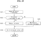
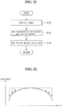
- the third luminance adjusting unit 54 receives the input of the user interface 110 and may be performed. As shown in FIG. 19 , the third luminance adjusting unit 54 adjusts the luminance of the display image based on the peripheral illuminance of the display device, thereby reducing the power consumption and preventing the glare of the user.
- the third luminance adjusting unit 54 adjusts the luminance of the display image using a third weight value ⁇ 3.
- the third weight value ⁇ 3 is set to be greater than zero and equal to or less than 1.
- the third multiplier 55 adjusts the luminances of the APL points p0 to p7 by multiplying the luminance of each of the APL points p0 to p7 received from the first multiplier 51 or the second multiplier 53 by the third weight value ⁇ 3.
- the fourth luminance adjusting unit 56 receives the input of the user interface 110 and may be performed.
- the fourth luminance adjusting unit 56 reduces the power consumption by gradually reducing the luminance as it goes from a middle portion of the screen or the pixel array of the display panel 10 to a peripheral portion thereof.
- the fourth luminance adjusting unit 56 outputs a fourth weight value ⁇ 4 for adjusting a luminance of the peripheral portion of the screen of the display panel 10.
- the fourth weight value ⁇ 4 is set to be greater than zero and equal to or less than 1.
- the fourth multiplier 57 adjusts the luminances of the APL points p0 to p7 by multiplying the luminance of each of the input APL points p0 to p7 by the fourth weight value ⁇ 4.
- the input APL points p0 to p7 of the fourth multiplier 57 are received from the first multiplier 51, the second multiplier 53, or the third multiplier 55.
- the fifth luminance adjusting unit 58 receives the input of the user interface 110 and may be performed.
- the fifth luminance adjusting unit 58 separately adjusts the luminance of the display image in a store mode and a home mode.
- the fifth luminance adjusting unit 58 causes the luminance of the display image in the store mode to be greater than the home mode because the lighting of the store, in which the display devices are displayed, is brighter than the indoor lighting of the home.
- the fifth luminance adjusting unit 58 outputs a fifth weight value ⁇ 5, which is set to different values in the store mode and the home mode.
- the fifth weight value ⁇ 5 may be set to 1.2 in the store mode and may be set to 1.0 in the home mode.
- the fifth multiplier 59 adjusts the luminances of the APL points p0 to p7 by multiplying the luminance of each of the APL points p0 to p7 by the fifth weight value ⁇ 5.
- the APL points p0 to p7 of the fifth multiplier 59 are received from one of the first to fourth multipliers 51, 53, 55, or 57.
- the set maker or the user may select the second to fifth luminance adjusting units 52, 54, 56, and 58 through the user interface 110.
- the luminance adjuster 104 sequentially adjusts the luminances of the APL points using at least one weight value output from the luminance adjusting unit the user selects. For example, as shown in FIGs. 6 to 8 , the APL point is multiplied by the first weight value and then may be multiplied by at least one of the second to fifth weight values.
- FIG. 9 shows APL points, which are positioned at regular intervals on the APL curve.
- FIG. 10 shows the APL curve adjusted by the luminance adjuster 104 shown in FIGs. 4 and 5 .
- FIG. 11 is a graph showing the luminance of the display image adjusted based on the APL curve.
- the APL curve date input to the luminance adjuster 104 may include only the N APL points p0 to p7 positioned at the boundaries between the neighboring sections.
- the luminance adjuster 104 adjusts the luminance of the APL at each of the N APL points p0 to p7 using the weight values ⁇ 1 to ⁇ 5, thereby reducing the luminance and the power consumption of the display image while minimizing a reduction in the image quality of the display image the user perceives.
- the maximum luminance of the display image having a value equal to or less than the APL at the first APL point p0 is fixed to a maximum value.
- the maximum luminance of the display image gradually is reduced. Further, the maximum luminance of the display image having a value greater than the APL at the eighth APL point p7 is fixed to a minimum value.
- the luminance adjuster 104 multiply the luminance of the APL curve data by the weight value to adjust the APL curve data APL' as shown in FIG. 10 .
- the luminance adjuster 104 transmits the APL curve data APL' to the timing controller 11 through a serial communication interface, for example, I 2 C communication.
- the timing controller 11 may transmit the luminance data of the APL points p0 to p7, which are previously determined through a test process so that the APL points p0 to p7 are optimized for the display panel, to the APL calculator 102 through the serial communication interface.
- the timing controller 11 modulates the gray level of the pixel data using the maximum luminance of the display image defined in the APL curve data APL'.
- the luminance of the display image changes depending on the gray level of the pixel data along 2.2 gamma curve as shown in FIG. 11 .
- the maximum luminance of the display image is equal to a maximum luminance defined in the APL curve data APL'.
- FIGs. 12 to 14 show an operation of the first luminance adjusting unit 50.
- the first luminance adjusting unit 50 adjusts the luminance of the display image in proportion to an input luminance (hereinafter referred to as "UI input luminance") of the user interface in steps S101 to 103.
- the first luminance adjusting unit 50 sets the first weight value ⁇ 1 for adjusting the maximum luminance of the display image.
- the first luminance adjusting unit 50 limits the minimum value of the maximum luminance of the display image to a value greater than zero.
- the first luminance adjusting unit 50 may fix the maximum luminance of the display image to not a value equal to or less than 10 % but a specific value equal to or greater than 10 % even if the UI input luminance is equal to or less than 10 %.
- the first weight value ⁇ 1 increases in proportion to the UI input luminance.
- the first weight value ⁇ 1 is set to 0.1 when the UI input luminance is equal to or less than 10 %.
- the first weight value ⁇ 1 may gradually increase within the range between 0.2 and 1.
- the first luminance adjusting unit 50 may adjust the APL curve data using the maximum luminance of the display image optimized in each image mode included in the previously set picture sound mode PSM.
- the picture sound mode PSM may include the vivid mode, the standard mode, the cinema mode, the game mode, etc.
- the maximum luminance and the contrast ratio of the display image may be differently set.
- the maximum luminance of the display image may be set to 100 % in the vivid mode, 70 % in the standard mode, 30 % in the cinema mode, and 60 % in the game mode.
- the first luminance adjusting unit 50 may adjust the luminance of each image mode included in the picture sound mode PSM using the first weight value ⁇ 1.
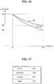
- FIGs. 15 to 17 show an operation of the second luminance adjusting unit 52.
- the second luminance adjusting unit 52 decides a motion of the input image and the input APL curve data and adjusts the luminance of the display image using the second weight value ⁇ 2 in steps S111, S112, and S115.
- the second luminance adjusting unit 52 analyzes the input image using a known motion estimation/motion compensation (MEMC) algorithm and may decide the motion of the input image using a calculated motion vector. Further, the second luminance adjusting unit 52 may decide the motion of the input image using the motion vector received along with the input image. As shown in FIG. 16 , the second luminance adjusting unit 52 reduces the maximum luminance of the display image using the second weight value ⁇ 2 as the motion of the input image increases.
- MEMC motion estimation/motion compensation
- the maximum luminance of the display image at the low APL curve data is less than that at the high APL curve data.
- the second luminance adjusting unit 52 controls the maximum luminance of the display image at the low APL curve to 50 % and controls the maximum luminance of the display image at the high APL curve to 65 %.
- the second luminance adjusting unit 52 may not adjust the maximum luminance of the display image in the low APL section where the input APL is equal to or less than the first APL point p0.
- the second luminance adjusting unit 52 may differently control the motion of the input image and the APL in each image mode included in the picture sound mode PSM.
- the second luminance adjusting unit 52 controls the luminance of the display image based on the low APL curve shown in FIG. 16 in the standard mode and does not adjust the luminance of the display image in the vivid mode, the cinema mode, and the game mode.
- the second luminance adjusting unit 52 does not adjust the luminance of the display image and maintains it in steps S113 and S114. This is because if the luminance of the display image is adjusted depending on the motion of the input image in the change of the scene, changes in the luminance of the display image may be greatly seen.
- the second luminance adjusting unit 52 calculates a histogram of the input image. Hence, when the histogram sharply changes as shown in (A) and (B) of FIG. 18 , the second luminance adjusting unit 52 may decide the sharp change of the histogram as timing of the scene change.
- the second luminance adjusting unit 52 sets the second weight value ⁇ 2 to 1 when the scene changes, and does not adjust the luminance of the display image in step S115.
- a horizontal axis is the gray level of the pixel data
- a vertical axis is the number of accumulated pixel data at each gray level.
- FIG. 19 is a flow chart showing an operation of the third luminance adjusting unit 54.
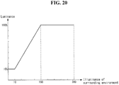
- FIG. 20 shows the luminance of the display image depending on the illuminance of the surrounding environment.
- the third luminance adjusting unit 54 receives an output signal of the illuminance sensor and decides the illuminance of the surrounding environment in step S121.
- the third luminance adjusting unit 54 adjusts the maximum luminance of the display image in proportion to the illuminance of the surrounding environment using the third weight value ⁇ 3 in some of the APL sections in steps S122 to 125. For example, as shown in FIG.
- the third luminance adjusting unit 54 increases the maximum luminance of the display image using the third weight value ⁇ 3 as the illuminance of the surrounding environment increases, and reduces the maximum luminance of the display image using the third weight value ⁇ 3 as the illuminance of the surrounding environment is reduced.
- the third luminance adjusting unit 54 maintains the maximum luminance of the display image to about 10 %.
- the third luminance adjusting unit 54 maintains the maximum luminance of the display image to about 100 %.
- the third luminance adjusting unit 54 may adjust the color temperature of the display image depending on the illuminance and the color temperature of the surrounding environment.
- the color temperature may be adjusted using the third weight value a3, which is independently set with respect to red (R), green (G), and blue (B) colors.
- the third luminance adjusting unit 54 may maintain the color temperature of the display image to a specific color temperature, for example, about 10,000 K.
- the third luminance adjusting unit 54 may adjust the color temperature of the display image to about 7,000 to 11,000 K.
- the third luminance adjusting unit 54 may maintain the color temperature of the display image to a specific color temperature, for example, about 11,000 K or 13,000 K.
- the third luminance adjusting unit 54 may adjust the color temperature of the display image in proportion to the color temperature of the surrounding environment. In other words, the third luminance adjusting unit 54 reduces the color temperature of the display image when the color temperature of the surrounding environment is lowered, and increases the color temperature of the display image when the color temperature of the surrounding environment increases.
- FIGs. 21 and 22 show an operation of the fourth luminance adjusting unit 56.
- the fourth luminance adjusting unit 56 calculates the fourth weight value a4, which gradually reduces the luminance of the display image as it goes from the middle portion of the screen of the display panel 10 or the screen of the display image to the peripheral portion. Namely, the fourth weight value a4 in the middle portion is greater than the fourth weight value a4 in the peripheral portion.
- the fourth weight value a4 may be calculated based on a result of the analysis of the input image in steps S131 to S133. For example, the fourth luminance adjusting unit 56 analyzes the complexity of the input image.
- the fourth luminance adjusting unit 56 greatly reduces the fourth weight value a4 to be applied to the peripheral portion of the screen when the input image has the relatively large complexity, and slightly reduces the fourth weight value a4 to be applied to the peripheral portion of the screen when the input image has the relatively small complexity. This is because the user is less sensitive to changes in the luminance of the display image when the complexity of the input image increases.
- the complexity of the input image may be calculated by the number of edges such as boundaries, or the number of recognizable colors, etc., but is not limited thereto.
- a portion of the luminance adjuster 104 may be embedded in the graphic controller of the host system 100, and the remaining portion may be embedded in the timing controller 11.
- a luminance adjuster 124 embedded in the host system 100 includes the first and third luminance adjusting units 50 and 54 and the first and third multipliers 51 and 55.
- the first luminance adjusting unit 50 sets the first weight value ⁇ 1 in response to the UI input luminance input through the user interface 110 and adjusts the luminance of the display image. In this instance, when the UI input luminance is zero, the maximum luminance of the display image is limited to a value greater than zero.
- the first multiplier 51 adjusts the luminance of the APL point by multiplying the luminance of the input APL by the first weight value ⁇ 1.
- the first luminance adjusting unit 50 may adjust the maximum luminance of the display image based on the picture sound mode PSM.
- the third luminance adjusting unit 54 adjusts the luminance of the display image based on the peripheral illuminance of the display device, thereby reducing the power consumption and preventing the user from glaring.
- the third luminance adjusting unit 54 adjusts the luminance of the display image using the third weight value ⁇ 3.
- the third multiplier 55 adjusts the luminance of the APL point by multiplying the luminance of the input APL received from the first multiplier 51 by the third weight value ⁇ 3.
- the luminance adjuster 124 transmits the pixel data of the input image and the APL curve data APL' including the APLs of the APL points p0 to p7 to the timing controller 11.
- the timing controller 11 includes a luminance adjuster 30, an interpolator 32, and a data modulator 34.
- the luminance adjuster 30 adjusts the APL point at each of the APL points of the APL curve data APL' received from the host system 100.
- the luminance adjuster 30 includes the second, fourth, and fifth luminance adjusting units 52, 56, and 58 and the second, fourth, and fifth multipliers 53, 57, and 59.
- the second luminance adjusting unit 52 adjusts the luminance of the display image based on the motion of the input image and the APL using the second weight value ⁇ 2 through the same method as FIGs. 15 to 18 .
- the second luminance adjusting unit 52 may not adjust the luminance of the display image when the scene changes.
- the second luminance adjusting unit 52 adjusts the luminance of the display image using the second weight value ⁇ 2.
- the second multiplier 53 adjusts the luminance of the APL point by multiplying the luminance of the input APL point by the second weight value ⁇ 2.
- the fourth luminance adjusting unit 56 gradually reduces the luminance using the fourth weight value a4 as it goes from the middle portion of the screen of the display panel 10 to the peripheral portion, thereby reducing the power consumption.
- the fourth multiplier 57 adjusts the luminance of the APL point by multiplying the luminance of the input APL point by the fourth weight value a4.
- the fifth luminance adjusting unit 58 causes the luminance of the display image in the store mode to be greater than the home mode using the fifth weight value a5.
- the fifth multiplier 59 adjusts the luminance of the APL point by multiplying the luminance of the input APL point by the fifth weight value a5.
- the interpolator 32 receives the APL points p0 to p7 from the fifth multiplier 59 and generates APL curve data APL" through the linear interpolation method.
- the interpolator 32 supplies the APL curve data APL" to the data modulator 34.
- the data modulator 34 modulates the gray levels of the pixel data of the input image based on the APL curve data APL" and thus may adjust the luminance or the color temperature of the display image.
- the embodiment of the invention selectively sets at least one luminance adjusting unit, which properly reduces the luminance of the display image displayed on the display panel in consideration of the image quality of the display device, using the user interface.
- the embodiment of the invention may minimize the reduction in the image quality of the display device and may reduce the power consumption.
Landscapes
- Engineering & Computer Science (AREA)
- Physics & Mathematics (AREA)
- Computer Hardware Design (AREA)
- General Physics & Mathematics (AREA)
- Theoretical Computer Science (AREA)
- Chemical & Material Sciences (AREA)
- Crystallography & Structural Chemistry (AREA)
- Control Of Indicators Other Than Cathode Ray Tubes (AREA)
Applications Claiming Priority (2)
| Application Number | Priority Date | Filing Date | Title |
|---|---|---|---|
| KR1020130105127A KR102083299B1 (ko) | 2013-09-02 | 2013-09-02 | 표시장치와 그 휘도 제어 방법 |
| PCT/KR2013/011611 WO2015030315A1 (ko) | 2013-09-02 | 2013-12-13 | 표시장치와 그 휘도 제어 방법 |
Publications (3)
| Publication Number | Publication Date |
|---|---|
| EP3043340A1 EP3043340A1 (en) | 2016-07-13 |
| EP3043340A4 EP3043340A4 (en) | 2017-01-25 |
| EP3043340B1 true EP3043340B1 (en) | 2019-04-17 |
Family
ID=52582592
Family Applications (1)
| Application Number | Title | Priority Date | Filing Date |
|---|---|---|---|
| EP13892154.9A Active EP3043340B1 (en) | 2013-09-02 | 2013-12-13 | Display device and method for controlling brightness thereof |
Country Status (5)
| Country | Link |
|---|---|
| US (1) | US9236017B2 (zh) |
| EP (1) | EP3043340B1 (zh) |
| KR (1) | KR102083299B1 (zh) |
| CN (1) | CN105493170B (zh) |
| WO (1) | WO2015030315A1 (zh) |
Families Citing this family (14)
| Publication number | Priority date | Publication date | Assignee | Title |
|---|---|---|---|---|
| KR20170031941A (ko) * | 2015-09-14 | 2017-03-22 | 엘지전자 주식회사 | 디스플레이 장치 및 그의 휘도 제어 방법 |
| US10248146B2 (en) * | 2015-10-14 | 2019-04-02 | Honeywell International Inc. | System for dynamic control with interactive visualization to optimize energy consumption |
| KR102486398B1 (ko) | 2015-10-14 | 2023-01-10 | 삼성디스플레이 주식회사 | 영상 신호 처리 회로 및 이를 포함하는 표시 장치 |
| US9832530B2 (en) * | 2016-05-02 | 2017-11-28 | Echostar Technologies L.L.C. | Reduce blue light at set-top box to assist with sleep |
| KR102588126B1 (ko) | 2016-11-01 | 2023-10-13 | 삼성전자주식회사 | 디스플레이 구동 회로 및 이를 포함하는 디스플레이 구동 시스템 |
| KR102637731B1 (ko) | 2017-12-26 | 2024-02-19 | 삼성전자주식회사 | 데이터 라인 구동 회로, 이를 포함하는 디스플레이 구동 회로 및 디스플레이 구동 방법 |
| CN108831381A (zh) * | 2018-06-25 | 2018-11-16 | 深圳市华星光电半导体显示技术有限公司 | 显示数据调整系统及显示数据调整方法 |
| US10802333B2 (en) * | 2018-08-21 | 2020-10-13 | Himax Technologies Limited | Local dimming system and method adaptable to a backlight of a display |
| US10586482B1 (en) * | 2019-03-04 | 2020-03-10 | Apple Inc. | Electronic device with ambient light sensor system |
| KR20220100759A (ko) | 2021-01-08 | 2022-07-18 | 삼성디스플레이 주식회사 | 복수의 표시 패널들을 가지는 타일드 표시 장치 |
| CN112863437B (zh) * | 2021-01-15 | 2022-09-06 | 海信视像科技股份有限公司 | 显示设备和亮度控制方法 |
| US11594199B2 (en) | 2021-04-30 | 2023-02-28 | Apple Inc. | Electronic device with multiple ambient light sensors |
| US20230066071A1 (en) * | 2021-09-02 | 2023-03-02 | Semiconductor Energy Laboratory Co., Ltd. | Image correction method and image correction system |
| KR20240042707A (ko) * | 2022-09-26 | 2024-04-02 | 엘지전자 주식회사 | 디스플레이 장치 및 그의 동작 방법 |
Family Cites Families (18)
| Publication number | Priority date | Publication date | Assignee | Title |
|---|---|---|---|---|
| JP4011743B2 (ja) * | 1998-07-24 | 2007-11-21 | 株式会社日立製作所 | 画像表示装置 |
| JP2002357810A (ja) * | 2001-05-31 | 2002-12-13 | Matsushita Electric Ind Co Ltd | 映像表示装置及び方法 |
| CN1307608C (zh) | 2001-04-25 | 2007-03-28 | 松下电器产业株式会社 | 图象显示装置及图象显示方法 |
| JP3783645B2 (ja) * | 2002-04-05 | 2006-06-07 | 株式会社日立製作所 | コントラスト調整方法、コントラスト調整回路及びそれを用いた映像表示装置 |
| KR20040083188A (ko) * | 2003-03-21 | 2004-10-01 | 엘지전자 주식회사 | 비대칭 셀 기반의 평균화상레벨 계산방법 및 장치 |
| JP2007264014A (ja) * | 2006-03-27 | 2007-10-11 | Pioneer Electronic Corp | 輝度制御装置、表示装置、輝度制御方法、そのプログラム、および、そのプログラムを記録した記録媒体 |
| JP2006251819A (ja) * | 2006-04-10 | 2006-09-21 | Sanyo Electric Co Ltd | 投写型映像表示装置 |
| CN100542236C (zh) * | 2006-07-03 | 2009-09-16 | 深圳Tcl工业研究院有限公司 | 液晶电视背光亮度调整方法 |
| JP5091796B2 (ja) * | 2008-08-05 | 2012-12-05 | 株式会社東芝 | 画像処理装置 |
| KR101307552B1 (ko) * | 2008-08-12 | 2013-09-12 | 엘지디스플레이 주식회사 | 액정표시장치와 그 구동방법 |
| KR20100052833A (ko) * | 2008-11-11 | 2010-05-20 | 엘지전자 주식회사 | 영상 표시 기기의 절전 장치 및 절전 모드 구현 방법 |
| JP5304211B2 (ja) * | 2008-12-11 | 2013-10-02 | ソニー株式会社 | 表示装置、輝度調整装置、バックライト装置、輝度調整方法及びプログラム |
| JP5321032B2 (ja) * | 2008-12-11 | 2013-10-23 | ソニー株式会社 | 表示装置、輝度調整装置、輝度調整方法及びプログラム |
| KR20110052120A (ko) * | 2009-11-12 | 2011-05-18 | 엘지전자 주식회사 | 플라즈마 디스플레이 패널의 구동 방법 및 장치 |
| JP2011128182A (ja) * | 2009-12-15 | 2011-06-30 | Sharp Corp | 表示装置 |
| KR101330396B1 (ko) * | 2010-06-25 | 2013-11-15 | 엘지디스플레이 주식회사 | 표시장치와 그의 콘트라스트 향상 방법 |
| CN103035193B (zh) * | 2012-12-20 | 2015-04-08 | 四川虹欧显示器件有限公司 | Pdp动态apl的控制方法 |
| KR102083297B1 (ko) * | 2013-09-02 | 2020-03-03 | 엘지전자 주식회사 | 표시장치와 그 휘도 제어 방법 |
-
2013
- 2013-09-02 KR KR1020130105127A patent/KR102083299B1/ko active IP Right Grant
- 2013-12-13 WO PCT/KR2013/011611 patent/WO2015030315A1/ko active Application Filing
- 2013-12-13 EP EP13892154.9A patent/EP3043340B1/en active Active
- 2013-12-13 CN CN201380079289.4A patent/CN105493170B/zh active Active
- 2013-12-30 US US14/143,521 patent/US9236017B2/en active Active
Non-Patent Citations (1)
| Title |
|---|
| None * |
Also Published As
| Publication number | Publication date |
|---|---|
| WO2015030315A1 (ko) | 2015-03-05 |
| CN105493170A (zh) | 2016-04-13 |
| CN105493170B (zh) | 2018-03-02 |
| EP3043340A4 (en) | 2017-01-25 |
| KR20150026376A (ko) | 2015-03-11 |
| EP3043340A1 (en) | 2016-07-13 |
| KR102083299B1 (ko) | 2020-03-03 |
| US20150062186A1 (en) | 2015-03-05 |
| US9236017B2 (en) | 2016-01-12 |
Similar Documents
| Publication | Publication Date | Title |
|---|---|---|
| EP3043340B1 (en) | Display device and method for controlling brightness thereof | |
| US9589499B2 (en) | Display device having function of controlling luminance based on average picture level and luminance control method thereof | |
| KR102146107B1 (ko) | 표시장치와 그 휘도 제어 방법 | |
| KR102412107B1 (ko) | 휘도 제어장치와 이를 포함하는 표시장치 | |
| US9412304B2 (en) | Display device and method for driving the same | |
| KR102113109B1 (ko) | 유기 발광 표시 장치의 구동 방법 및 유기 발광 표시 장치 | |
| KR102154698B1 (ko) | 표시장치와 그 휘도 향상 방법 | |
| KR20200128283A (ko) | 표시 장치 및 이의 구동 방법 | |
| KR20170021678A (ko) | 표시장치 및 그의 데이터 보상방법 | |
| KR102106559B1 (ko) | 감마 보상 방법과 이를 이용한 표시장치 | |
| KR102215986B1 (ko) | 소비 전력 제어 방법 및 장치와 이를 이용한 표시장치 | |
| KR102237138B1 (ko) | 표시장치와 그 휘도 제어 방법 | |
| KR101936679B1 (ko) | 유기발광표시장치 및 그 구동방법 | |
| KR102611009B1 (ko) | 타이밍 콘트롤러와 이를 이용한 표시장치 | |
| KR102387345B1 (ko) | 입력영상 처리회로 및 이를 포함하는 표시장치 | |
| US20220375388A1 (en) | Systems and Methods for Brightness or Color Control in Foldable Displays | |
| KR102218460B1 (ko) | 표시장치와 그 시인성 향상 방법 | |
| KR102231156B1 (ko) | 표시장치와 그 데이터 보상 방법 | |
| KR102116056B1 (ko) | 색온도 변환방법과 이를 이용한 표시장치 |
Legal Events
| Date | Code | Title | Description |
|---|---|---|---|
| PUAI | Public reference made under article 153(3) epc to a published international application that has entered the european phase |
Free format text: ORIGINAL CODE: 0009012 |
|
| 17P | Request for examination filed |
Effective date: 20160215 |
|
| AK | Designated contracting states |
Kind code of ref document: A1 Designated state(s): AL AT BE BG CH CY CZ DE DK EE ES FI FR GB GR HR HU IE IS IT LI LT LU LV MC MK MT NL NO PL PT RO RS SE SI SK SM TR |
|
| AX | Request for extension of the european patent |
Extension state: BA ME |
|
| DAX | Request for extension of the european patent (deleted) | ||
| A4 | Supplementary search report drawn up and despatched |
Effective date: 20161223 |
|
| RIC1 | Information provided on ipc code assigned before grant |
Ipc: G09G 5/10 20060101ALI20161219BHEP Ipc: G09G 3/32 20160101AFI20161219BHEP |
|
| STAA | Information on the status of an ep patent application or granted ep patent |
Free format text: STATUS: EXAMINATION IS IN PROGRESS |
|
| 17Q | First examination report despatched |
Effective date: 20180404 |
|
| GRAP | Despatch of communication of intention to grant a patent |
Free format text: ORIGINAL CODE: EPIDOSNIGR1 |
|
| STAA | Information on the status of an ep patent application or granted ep patent |
Free format text: STATUS: GRANT OF PATENT IS INTENDED |
|
| INTG | Intention to grant announced |
Effective date: 20181114 |
|
| GRAS | Grant fee paid |
Free format text: ORIGINAL CODE: EPIDOSNIGR3 |
|
| GRAA | (expected) grant |
Free format text: ORIGINAL CODE: 0009210 |
|
| STAA | Information on the status of an ep patent application or granted ep patent |
Free format text: STATUS: THE PATENT HAS BEEN GRANTED |
|
| AK | Designated contracting states |
Kind code of ref document: B1 Designated state(s): AL AT BE BG CH CY CZ DE DK EE ES FI FR GB GR HR HU IE IS IT LI LT LU LV MC MK MT NL NO PL PT RO RS SE SI SK SM TR |
|
| REG | Reference to a national code |
Ref country code: GB Ref legal event code: FG4D |
|
| REG | Reference to a national code |
Ref country code: CH Ref legal event code: EP |
|
| REG | Reference to a national code |
Ref country code: DE Ref legal event code: R096 Ref document number: 602013054149 Country of ref document: DE |
|
| REG | Reference to a national code |
Ref country code: AT Ref legal event code: REF Ref document number: 1122417 Country of ref document: AT Kind code of ref document: T Effective date: 20190515 Ref country code: IE Ref legal event code: FG4D |
|
| REG | Reference to a national code |
Ref country code: NL Ref legal event code: MP Effective date: 20190417 |
|
| REG | Reference to a national code |
Ref country code: LT Ref legal event code: MG4D |
|
| PG25 | Lapsed in a contracting state [announced via postgrant information from national office to epo] |
Ref country code: NL Free format text: LAPSE BECAUSE OF FAILURE TO SUBMIT A TRANSLATION OF THE DESCRIPTION OR TO PAY THE FEE WITHIN THE PRESCRIBED TIME-LIMIT Effective date: 20190417 |
|
| PG25 | Lapsed in a contracting state [announced via postgrant information from national office to epo] |
Ref country code: HR Free format text: LAPSE BECAUSE OF FAILURE TO SUBMIT A TRANSLATION OF THE DESCRIPTION OR TO PAY THE FEE WITHIN THE PRESCRIBED TIME-LIMIT Effective date: 20190417 Ref country code: LT Free format text: LAPSE BECAUSE OF FAILURE TO SUBMIT A TRANSLATION OF THE DESCRIPTION OR TO PAY THE FEE WITHIN THE PRESCRIBED TIME-LIMIT Effective date: 20190417 Ref country code: SE Free format text: LAPSE BECAUSE OF FAILURE TO SUBMIT A TRANSLATION OF THE DESCRIPTION OR TO PAY THE FEE WITHIN THE PRESCRIBED TIME-LIMIT Effective date: 20190417 Ref country code: NO Free format text: LAPSE BECAUSE OF FAILURE TO SUBMIT A TRANSLATION OF THE DESCRIPTION OR TO PAY THE FEE WITHIN THE PRESCRIBED TIME-LIMIT Effective date: 20190717 Ref country code: FI Free format text: LAPSE BECAUSE OF FAILURE TO SUBMIT A TRANSLATION OF THE DESCRIPTION OR TO PAY THE FEE WITHIN THE PRESCRIBED TIME-LIMIT Effective date: 20190417 Ref country code: AL Free format text: LAPSE BECAUSE OF FAILURE TO SUBMIT A TRANSLATION OF THE DESCRIPTION OR TO PAY THE FEE WITHIN THE PRESCRIBED TIME-LIMIT Effective date: 20190417 Ref country code: PT Free format text: LAPSE BECAUSE OF FAILURE TO SUBMIT A TRANSLATION OF THE DESCRIPTION OR TO PAY THE FEE WITHIN THE PRESCRIBED TIME-LIMIT Effective date: 20190817 Ref country code: ES Free format text: LAPSE BECAUSE OF FAILURE TO SUBMIT A TRANSLATION OF THE DESCRIPTION OR TO PAY THE FEE WITHIN THE PRESCRIBED TIME-LIMIT Effective date: 20190417 |
|
| PG25 | Lapsed in a contracting state [announced via postgrant information from national office to epo] |
Ref country code: BG Free format text: LAPSE BECAUSE OF FAILURE TO SUBMIT A TRANSLATION OF THE DESCRIPTION OR TO PAY THE FEE WITHIN THE PRESCRIBED TIME-LIMIT Effective date: 20190717 Ref country code: GR Free format text: LAPSE BECAUSE OF FAILURE TO SUBMIT A TRANSLATION OF THE DESCRIPTION OR TO PAY THE FEE WITHIN THE PRESCRIBED TIME-LIMIT Effective date: 20190718 Ref country code: RS Free format text: LAPSE BECAUSE OF FAILURE TO SUBMIT A TRANSLATION OF THE DESCRIPTION OR TO PAY THE FEE WITHIN THE PRESCRIBED TIME-LIMIT Effective date: 20190417 Ref country code: PL Free format text: LAPSE BECAUSE OF FAILURE TO SUBMIT A TRANSLATION OF THE DESCRIPTION OR TO PAY THE FEE WITHIN THE PRESCRIBED TIME-LIMIT Effective date: 20190417 Ref country code: LV Free format text: LAPSE BECAUSE OF FAILURE TO SUBMIT A TRANSLATION OF THE DESCRIPTION OR TO PAY THE FEE WITHIN THE PRESCRIBED TIME-LIMIT Effective date: 20190417 |
|
| REG | Reference to a national code |
Ref country code: AT Ref legal event code: MK05 Ref document number: 1122417 Country of ref document: AT Kind code of ref document: T Effective date: 20190417 |
|
| PG25 | Lapsed in a contracting state [announced via postgrant information from national office to epo] |
Ref country code: IS Free format text: LAPSE BECAUSE OF FAILURE TO SUBMIT A TRANSLATION OF THE DESCRIPTION OR TO PAY THE FEE WITHIN THE PRESCRIBED TIME-LIMIT Effective date: 20190817 |
|
| REG | Reference to a national code |
Ref country code: DE Ref legal event code: R097 Ref document number: 602013054149 Country of ref document: DE |
|
| PG25 | Lapsed in a contracting state [announced via postgrant information from national office to epo] |
Ref country code: EE Free format text: LAPSE BECAUSE OF FAILURE TO SUBMIT A TRANSLATION OF THE DESCRIPTION OR TO PAY THE FEE WITHIN THE PRESCRIBED TIME-LIMIT Effective date: 20190417 Ref country code: DK Free format text: LAPSE BECAUSE OF FAILURE TO SUBMIT A TRANSLATION OF THE DESCRIPTION OR TO PAY THE FEE WITHIN THE PRESCRIBED TIME-LIMIT Effective date: 20190417 Ref country code: RO Free format text: LAPSE BECAUSE OF FAILURE TO SUBMIT A TRANSLATION OF THE DESCRIPTION OR TO PAY THE FEE WITHIN THE PRESCRIBED TIME-LIMIT Effective date: 20190417 Ref country code: AT Free format text: LAPSE BECAUSE OF FAILURE TO SUBMIT A TRANSLATION OF THE DESCRIPTION OR TO PAY THE FEE WITHIN THE PRESCRIBED TIME-LIMIT Effective date: 20190417 Ref country code: CZ Free format text: LAPSE BECAUSE OF FAILURE TO SUBMIT A TRANSLATION OF THE DESCRIPTION OR TO PAY THE FEE WITHIN THE PRESCRIBED TIME-LIMIT Effective date: 20190417 Ref country code: SK Free format text: LAPSE BECAUSE OF FAILURE TO SUBMIT A TRANSLATION OF THE DESCRIPTION OR TO PAY THE FEE WITHIN THE PRESCRIBED TIME-LIMIT Effective date: 20190417 |
|
| PLBE | No opposition filed within time limit |
Free format text: ORIGINAL CODE: 0009261 |
|
| STAA | Information on the status of an ep patent application or granted ep patent |
Free format text: STATUS: NO OPPOSITION FILED WITHIN TIME LIMIT |
|
| PG25 | Lapsed in a contracting state [announced via postgrant information from national office to epo] |
Ref country code: SM Free format text: LAPSE BECAUSE OF FAILURE TO SUBMIT A TRANSLATION OF THE DESCRIPTION OR TO PAY THE FEE WITHIN THE PRESCRIBED TIME-LIMIT Effective date: 20190417 Ref country code: IT Free format text: LAPSE BECAUSE OF FAILURE TO SUBMIT A TRANSLATION OF THE DESCRIPTION OR TO PAY THE FEE WITHIN THE PRESCRIBED TIME-LIMIT Effective date: 20190417 |
|
| 26N | No opposition filed |
Effective date: 20200120 |
|
| PG25 | Lapsed in a contracting state [announced via postgrant information from national office to epo] |
Ref country code: TR Free format text: LAPSE BECAUSE OF FAILURE TO SUBMIT A TRANSLATION OF THE DESCRIPTION OR TO PAY THE FEE WITHIN THE PRESCRIBED TIME-LIMIT Effective date: 20190417 |
|
| PG25 | Lapsed in a contracting state [announced via postgrant information from national office to epo] |
Ref country code: SI Free format text: LAPSE BECAUSE OF FAILURE TO SUBMIT A TRANSLATION OF THE DESCRIPTION OR TO PAY THE FEE WITHIN THE PRESCRIBED TIME-LIMIT Effective date: 20190417 |
|
| REG | Reference to a national code |
Ref country code: CH Ref legal event code: PL |
|
| REG | Reference to a national code |
Ref country code: BE Ref legal event code: MM Effective date: 20191231 |
|
| PG25 | Lapsed in a contracting state [announced via postgrant information from national office to epo] |
Ref country code: MC Free format text: LAPSE BECAUSE OF FAILURE TO SUBMIT A TRANSLATION OF THE DESCRIPTION OR TO PAY THE FEE WITHIN THE PRESCRIBED TIME-LIMIT Effective date: 20190417 |
|
| PG25 | Lapsed in a contracting state [announced via postgrant information from national office to epo] |
Ref country code: IE Free format text: LAPSE BECAUSE OF NON-PAYMENT OF DUE FEES Effective date: 20191213 Ref country code: LU Free format text: LAPSE BECAUSE OF NON-PAYMENT OF DUE FEES Effective date: 20191213 |
|
| PG25 | Lapsed in a contracting state [announced via postgrant information from national office to epo] |
Ref country code: LI Free format text: LAPSE BECAUSE OF NON-PAYMENT OF DUE FEES Effective date: 20191231 Ref country code: BE Free format text: LAPSE BECAUSE OF NON-PAYMENT OF DUE FEES Effective date: 20191231 Ref country code: CH Free format text: LAPSE BECAUSE OF NON-PAYMENT OF DUE FEES Effective date: 20191231 |
|
| PG25 | Lapsed in a contracting state [announced via postgrant information from national office to epo] |
Ref country code: CY Free format text: LAPSE BECAUSE OF FAILURE TO SUBMIT A TRANSLATION OF THE DESCRIPTION OR TO PAY THE FEE WITHIN THE PRESCRIBED TIME-LIMIT Effective date: 20190417 |
|
| PG25 | Lapsed in a contracting state [announced via postgrant information from national office to epo] |
Ref country code: MT Free format text: LAPSE BECAUSE OF FAILURE TO SUBMIT A TRANSLATION OF THE DESCRIPTION OR TO PAY THE FEE WITHIN THE PRESCRIBED TIME-LIMIT Effective date: 20190417 Ref country code: HU Free format text: LAPSE BECAUSE OF FAILURE TO SUBMIT A TRANSLATION OF THE DESCRIPTION OR TO PAY THE FEE WITHIN THE PRESCRIBED TIME-LIMIT; INVALID AB INITIO Effective date: 20131213 |
|
| PG25 | Lapsed in a contracting state [announced via postgrant information from national office to epo] |
Ref country code: MK Free format text: LAPSE BECAUSE OF FAILURE TO SUBMIT A TRANSLATION OF THE DESCRIPTION OR TO PAY THE FEE WITHIN THE PRESCRIBED TIME-LIMIT Effective date: 20190417 |
|
| PGFP | Annual fee paid to national office [announced via postgrant information from national office to epo] |
Ref country code: GB Payment date: 20231106 Year of fee payment: 11 |
|
| PGFP | Annual fee paid to national office [announced via postgrant information from national office to epo] |
Ref country code: FR Payment date: 20231107 Year of fee payment: 11 Ref country code: DE Payment date: 20231106 Year of fee payment: 11 |