EP3040973A1 - Display device - Google Patents
Display device Download PDFInfo
- Publication number
- EP3040973A1 EP3040973A1 EP15202889.0A EP15202889A EP3040973A1 EP 3040973 A1 EP3040973 A1 EP 3040973A1 EP 15202889 A EP15202889 A EP 15202889A EP 3040973 A1 EP3040973 A1 EP 3040973A1
- Authority
- EP
- European Patent Office
- Prior art keywords
- data
- image data
- current
- display device
- change
- Prior art date
- Legal status (The legal status is an assumption and is not a legal conclusion. Google has not performed a legal analysis and makes no representation as to the accuracy of the status listed.)
- Granted
Links
Images




Classifications
-
- G—PHYSICS
- G09—EDUCATION; CRYPTOGRAPHY; DISPLAY; ADVERTISING; SEALS
- G09G—ARRANGEMENTS OR CIRCUITS FOR CONTROL OF INDICATING DEVICES USING STATIC MEANS TO PRESENT VARIABLE INFORMATION
- G09G3/00—Control arrangements or circuits, of interest only in connection with visual indicators other than cathode-ray tubes
- G09G3/20—Control arrangements or circuits, of interest only in connection with visual indicators other than cathode-ray tubes for presentation of an assembly of a number of characters, e.g. a page, by composing the assembly by combination of individual elements arranged in a matrix no fixed position being assigned to or needed to be assigned to the individual characters or partial characters
-
- G—PHYSICS
- G09—EDUCATION; CRYPTOGRAPHY; DISPLAY; ADVERTISING; SEALS
- G09G—ARRANGEMENTS OR CIRCUITS FOR CONTROL OF INDICATING DEVICES USING STATIC MEANS TO PRESENT VARIABLE INFORMATION
- G09G3/00—Control arrangements or circuits, of interest only in connection with visual indicators other than cathode-ray tubes
- G09G3/20—Control arrangements or circuits, of interest only in connection with visual indicators other than cathode-ray tubes for presentation of an assembly of a number of characters, e.g. a page, by composing the assembly by combination of individual elements arranged in a matrix no fixed position being assigned to or needed to be assigned to the individual characters or partial characters
- G09G3/22—Control arrangements or circuits, of interest only in connection with visual indicators other than cathode-ray tubes for presentation of an assembly of a number of characters, e.g. a page, by composing the assembly by combination of individual elements arranged in a matrix no fixed position being assigned to or needed to be assigned to the individual characters or partial characters using controlled light sources
- G09G3/30—Control arrangements or circuits, of interest only in connection with visual indicators other than cathode-ray tubes for presentation of an assembly of a number of characters, e.g. a page, by composing the assembly by combination of individual elements arranged in a matrix no fixed position being assigned to or needed to be assigned to the individual characters or partial characters using controlled light sources using electroluminescent panels
- G09G3/32—Control arrangements or circuits, of interest only in connection with visual indicators other than cathode-ray tubes for presentation of an assembly of a number of characters, e.g. a page, by composing the assembly by combination of individual elements arranged in a matrix no fixed position being assigned to or needed to be assigned to the individual characters or partial characters using controlled light sources using electroluminescent panels semiconductive, e.g. using light-emitting diodes [LED]
- G09G3/3208—Control arrangements or circuits, of interest only in connection with visual indicators other than cathode-ray tubes for presentation of an assembly of a number of characters, e.g. a page, by composing the assembly by combination of individual elements arranged in a matrix no fixed position being assigned to or needed to be assigned to the individual characters or partial characters using controlled light sources using electroluminescent panels semiconductive, e.g. using light-emitting diodes [LED] organic, e.g. using organic light-emitting diodes [OLED]
- G09G3/3275—Details of drivers for data electrodes
- G09G3/3283—Details of drivers for data electrodes in which the data driver supplies a variable data current for setting the current through, or the voltage across, the light-emitting elements
-
- G—PHYSICS
- G09—EDUCATION; CRYPTOGRAPHY; DISPLAY; ADVERTISING; SEALS
- G09G—ARRANGEMENTS OR CIRCUITS FOR CONTROL OF INDICATING DEVICES USING STATIC MEANS TO PRESENT VARIABLE INFORMATION
- G09G3/00—Control arrangements or circuits, of interest only in connection with visual indicators other than cathode-ray tubes
- G09G3/20—Control arrangements or circuits, of interest only in connection with visual indicators other than cathode-ray tubes for presentation of an assembly of a number of characters, e.g. a page, by composing the assembly by combination of individual elements arranged in a matrix no fixed position being assigned to or needed to be assigned to the individual characters or partial characters
- G09G3/2003—Display of colours
-
- G—PHYSICS
- G09—EDUCATION; CRYPTOGRAPHY; DISPLAY; ADVERTISING; SEALS
- G09G—ARRANGEMENTS OR CIRCUITS FOR CONTROL OF INDICATING DEVICES USING STATIC MEANS TO PRESENT VARIABLE INFORMATION
- G09G3/00—Control arrangements or circuits, of interest only in connection with visual indicators other than cathode-ray tubes
- G09G3/20—Control arrangements or circuits, of interest only in connection with visual indicators other than cathode-ray tubes for presentation of an assembly of a number of characters, e.g. a page, by composing the assembly by combination of individual elements arranged in a matrix no fixed position being assigned to or needed to be assigned to the individual characters or partial characters
- G09G3/34—Control arrangements or circuits, of interest only in connection with visual indicators other than cathode-ray tubes for presentation of an assembly of a number of characters, e.g. a page, by composing the assembly by combination of individual elements arranged in a matrix no fixed position being assigned to or needed to be assigned to the individual characters or partial characters by control of light from an independent source
- G09G3/36—Control arrangements or circuits, of interest only in connection with visual indicators other than cathode-ray tubes for presentation of an assembly of a number of characters, e.g. a page, by composing the assembly by combination of individual elements arranged in a matrix no fixed position being assigned to or needed to be assigned to the individual characters or partial characters by control of light from an independent source using liquid crystals
-
- G—PHYSICS
- G09—EDUCATION; CRYPTOGRAPHY; DISPLAY; ADVERTISING; SEALS
- G09G—ARRANGEMENTS OR CIRCUITS FOR CONTROL OF INDICATING DEVICES USING STATIC MEANS TO PRESENT VARIABLE INFORMATION
- G09G2310/00—Command of the display device
- G09G2310/02—Addressing, scanning or driving the display screen or processing steps related thereto
- G09G2310/0264—Details of driving circuits
- G09G2310/0275—Details of drivers for data electrodes, other than drivers for liquid crystal, plasma or OLED displays, not related to handling digital grey scale data or to communication of data to the pixels by means of a current
-
- G—PHYSICS
- G09—EDUCATION; CRYPTOGRAPHY; DISPLAY; ADVERTISING; SEALS
- G09G—ARRANGEMENTS OR CIRCUITS FOR CONTROL OF INDICATING DEVICES USING STATIC MEANS TO PRESENT VARIABLE INFORMATION
- G09G2320/00—Control of display operating conditions
- G09G2320/02—Improving the quality of display appearance
- G09G2320/0271—Adjustment of the gradation levels within the range of the gradation scale, e.g. by redistribution or clipping
- G09G2320/0276—Adjustment of the gradation levels within the range of the gradation scale, e.g. by redistribution or clipping for the purpose of adaptation to the characteristics of a display device, i.e. gamma correction
-
- G—PHYSICS
- G09—EDUCATION; CRYPTOGRAPHY; DISPLAY; ADVERTISING; SEALS
- G09G—ARRANGEMENTS OR CIRCUITS FOR CONTROL OF INDICATING DEVICES USING STATIC MEANS TO PRESENT VARIABLE INFORMATION
- G09G2330/00—Aspects of power supply; Aspects of display protection and defect management
- G09G2330/02—Details of power systems and of start or stop of display operation
- G09G2330/021—Power management, e.g. power saving
-
- G—PHYSICS
- G09—EDUCATION; CRYPTOGRAPHY; DISPLAY; ADVERTISING; SEALS
- G09G—ARRANGEMENTS OR CIRCUITS FOR CONTROL OF INDICATING DEVICES USING STATIC MEANS TO PRESENT VARIABLE INFORMATION
- G09G2330/00—Aspects of power supply; Aspects of display protection and defect management
- G09G2330/02—Details of power systems and of start or stop of display operation
- G09G2330/028—Generation of voltages supplied to electrode drivers in a matrix display other than LCD
-
- G—PHYSICS
- G09—EDUCATION; CRYPTOGRAPHY; DISPLAY; ADVERTISING; SEALS
- G09G—ARRANGEMENTS OR CIRCUITS FOR CONTROL OF INDICATING DEVICES USING STATIC MEANS TO PRESENT VARIABLE INFORMATION
- G09G2370/00—Aspects of data communication
- G09G2370/08—Details of image data interface between the display device controller and the data line driver circuit
-
- G—PHYSICS
- G09—EDUCATION; CRYPTOGRAPHY; DISPLAY; ADVERTISING; SEALS
- G09G—ARRANGEMENTS OR CIRCUITS FOR CONTROL OF INDICATING DEVICES USING STATIC MEANS TO PRESENT VARIABLE INFORMATION
- G09G2370/00—Aspects of data communication
- G09G2370/14—Use of low voltage differential signaling [LVDS] for display data communication
Definitions
- Embodiments of the invention relate to a display device and to method for operating a display device.
- Examples of a flat panel display include a liquid crystal display (LCD), a field emission display (FED), a plasma display panel (PDP), and an organic light emitting diode (OLED) display.
- LCD liquid crystal display
- FED field emission display
- PDP plasma display panel
- OLED organic light emitting diode
- data lines and gate lines are arranged to cross each other, and each crossing of the data lines and the gate lines is defined as a pixel.
- the plurality of pixels are formed on a display panel of the flat panel display in a matrix form.
- the flat panel display supplies a video data voltage to the data lines and sequentially supplies a gate pulse to the gate lines, thereby driving the pixels.
- the flat panel display supplies the video data voltage to the pixels of a gate line, to which the gate pulse is supplied, and sequentially scans all of the gate lines through the gate pulse, thereby displaying video data.
- a timing controller of a display device supplies digital video data, a clock for sampling the digital video data, a control signal for controlling operations of source driver integrated circuits (ICs), etc. to the source driver ICs through an interface such as low-voltage differential signaling (LVDS).
- the source driver ICs convert the digital video data serially received from the timing controller into parallel data and then convert the parallel data into an analog data voltage using a gamma compensation voltage.
- the source driver ICs supply the analog data voltages to the data lines, respectively.
- the LVDS interface method produces a differential signal using a current output from a current source of a differential signaling driver.
- the LVDS interface method increases power consumption in a process for increasing reliability of data transmission.
- a data driver of the display device includes various buffers. Because a bias current of each buffer is fixed to a predetermined value, the data driver uses more than necessary consumption current.
- a main idea of the invention is to analyze the input image data and to control the amount of current used for driving the data lines based on this analysis.
- a display device comprising a display panel including data lines; a data driver configured to produce a data voltage corresponding to input image data and supply the data voltage to the data lines; and a current controller configured to determine an amount of change in the input image data and to control a current used in the data driver to drive the data lines based on the amount of change in the image data.
- the display device comprises a differential signaling driver configured to produce a differential signal using a variable current; first and second signal lines configured to maintain a loop current in response to a signal output by the differential signaling driver; wherein the current controller is configured to reduce the variable current when one of low data and high data of image data is equal to or greater than a critical value; and a receiving unit configured to receive the differential signal through the first and second signal lines.
- a differential signaling driver configured to produce a differential signal using a variable current
- first and second signal lines configured to maintain a loop current in response to a signal output by the differential signaling driver
- the current controller is configured to reduce the variable current when one of low data and high data of image data is equal to or greater than a critical value
- a receiving unit configured to receive the differential signal through the first and second signal lines.
- the current controller may divide the image data into unit data of a predetermined number of bits and may reduce the variable current when a further predetermined number of data or more bits is the same in any one unit data among the unit data.
- the current controller is adapted to divide the image data into unit data of 8 bits and to reduce the variable current when unit data has the same six or more bits upper bits.
- the current controller may divide each of red image data, green image data, and blue image data into unit data of 8 bits and to reduce the variable current when the red image data, the green image data, and the blue image data have the same six upper bits.
- the receiving unit may set a terminating resistance depending on the loop current.
- a terminating resistor may be positioned between the first and second signal lines, wherein the current controller may adjust a resistance of the terminating resistor so that the resistance of the terminating resistor is inversely proportional to the variable current.
- the data driver is configured to produce a data voltage corresponding to input image data and to supply the data voltage to the data lines through an output buffer; wherein another current controller is configured to calculate an amount of change in the image data in the same channel and to vary a bias current of the output buffer based on the amount of change in the image data.
- the one and another current controller could be the same or separate current controllers.
- the current controller may perform an operation reducing the bias current of the output buffer as the amount of change in the image data decreases.
- the data driver may receive a gamma reference voltage through a gamma buffer so as to convert the image data into the data voltage, wherein the current controller is adapted to perform an operation reducing a bias current of the gamma buffer as the amount of change in the image data decreases.
- the data driver may receive a high potential voltage through a driving voltage output buffer, wherein the current controller may perform an operation reducing a bias current of the driving voltage output buffer as the amount of change in the image data decreases.
- the display device may comprise at least one source driver IC (SIC) including: a shift register, a latch, a digital-to-analog converter, and an output buffer.
- SIC source driver IC
- a method for operating a display device comprising the steps of: receiving input image data, analyzing the image data, determining toggling of the image data or amount of change of input image data, controlling a current for driving based on the determined toggling of the image data or amount of change of input data.
- the method further comprises the step of: if toggling of image data is lower than a critical value output a first control signal, or if toggling of image data is higher than a critical value output a second control signal, setting a loop current of a differential signaling driver of the display device based on the first or second control signal.
- the method further comprises the step of: producing a data voltage corresponding to input image data, and calculating an amount of change in the image data in the same channel and varying a bias current of an output buffer based on the amount of change in the image data, supplying the data voltage to the data lines through an output buffer.
- a display device comprising a differential signaling driver configured to produce a differential signal using a variable current, first and second signal lines configured to maintain a loop current in response to a signal output by the differential signaling driver, a current controller configured to reduce the variable current when one of low data and high data of image data is equal to or greater than a critical value, and a receiving unit configured to receive the differential signal through the first and second signal lines.
- a display device comprising a display panel including data lines, a data driver configured to produce a data voltage corresponding to input image data and supply the data voltage to the data lines through an output buffer, and a current controller configured to calculate an amount of change in the image data in the same channel and vary a bias current of the output buffer based on the amount of change in the image data.
- a liquid crystal display includes a liquid crystal display panel LCP, a timing controller TCON, source driver integrated circuits (ICs) SIC#1 to SIC#8, and gate driver ICs GIC.
- LCP liquid crystal display panel
- TCON timing controller
- ICs source driver integrated circuits
- GIC gate driver ICs
- a liquid crystal layer is formed between substrates of the liquid crystal display panel LCP.
- the liquid crystal display panel LCP includes liquid crystal cells Clc arranged in a matrix form based on a crossing structure of data lines DL and gate lines GL.
- a pixel array including the data lines DL, the gate lines GL, thin film transistors (TFTs), storage capacitors Cst, etc. is formed on a TFT array substrate of the liquid crystal display panel LCP.
- Each liquid crystal cell Clc is driven by an electric field between a pixel electrode, to which a data voltage is supplied through the TFT, and a common electrode, to which a common voltage Vcom is supplied.
- a gate electrode of the TFT is connected to the gate line GL, and a drain electrode of the TFT is connected to the data line DL.
- a source electrode of the TFT is connected to the pixel electrode of the liquid crystal cell Clc.
- the TFT is turned on in response to a gate pulse supplied through the gate line GL and supplies the data voltage from the data line DL to the pixel electrode of the liquid crystal cell Clc.
- Black matrixes, color filters, the common electrode, etc. are formed on a color filter substrate of the liquid crystal display panel LCP.
- Polarizing plates are respectively attached to the TFT array substrate and the color filter substrate of the liquid crystal display panel LCP.
- Alignment layers for setting a pre-tilt angle of liquid crystals are respectively formed on the TFT array substrate and the color filter substrate of the liquid crystal display panel LCP.
- a spacer may be formed between the TFT array substrate and the color filter substrate of the liquid crystal display panel LCP to keep cell gaps of the liquid crystal cells Clc constant.
- the timing controller TCON receives external timing signals, such as a vertical sync signal Vsync, a horizontal sync signal Hsync, an external data enable signal DE, and an external clock CLK, from an external host system (not shown) through an interface, such as a low-voltage differential signaling (LVDS) interface and a transition minimized differential signaling (TMDS) interface.
- external timing signals such as a vertical sync signal Vsync, a horizontal sync signal Hsync, an external data enable signal DE, and an external clock CLK
- LVDS low-voltage differential signaling
- TMDS transition minimized differential signaling
- a differential signaling driver of the timing controller TCON transmits the external clock CLK and RGB digital video data to the source driver ICs SIC#1 to SIC#8 through pairs of data lines.
- the timing controller TCON generates control data as a differential signal and may transmit the differential signal to the source driver ICs SIC#1 to SIC#8 through the pairs of data lines.
- the control data includes source control data for controlling output timing, a polarity, etc. of the data voltage output from the source driver ICs SIC#1 to SIC#8.
- the control data may include gate control data for controlling operation timing of the gate driver ICs GIC.
- the source driver ICs SIC#1 to SIC#8 receive the external clock CLK, the RGB digital video data, and the control data through the pairs of data lines.
- the source driver ICs SIC#1 to SIC#8 generate a frequency of the external clock CLK as internal clocks of ⁇ (the number of bits of RGB digital video data) ⁇ 2 ⁇ using a phase locked loop (PLL) or a delay locked loop (DLL).
- PLL phase locked loop
- DLL delay locked loop
- the source driver ICs SIC#1 to SIC#8 sample the RGB digital video data based on the internal clocks and then convert the sampled data into parallel data.
- the source driver ICs SIC#1 to SIC#8 decode the control data input through the pairs of data lines using a code mapping method and recover the source control data and the gate control data.
- the source driver ICs SIC#1 to SIC#8 convert the RGB digital video parallel data into positive and negative analog video data voltages in response to the recovered source control data and supply the data voltages to the data lines DL of the liquid crystal display panel LCP.
- the source driver ICs SIC#1 to SIC#8 may transmit the gate control data to at least one of the gate driver ICs GIC.
- the gate driver IC GIC sequentially supplies a gate pulse to the gate lines GL in response to the gate control data, that is received from the timing controller TCON or is received through the source driver ICs SIC#1 to SIC#8.
- the gate control data includes a gate start pulse GSP, a gate shift clock GSC, a gate output enable signal GOE, and the like.
- the gate start pulse GSP controls a start horizontal line of a scan operation during one vertical period in which one screen is displayed.
- the gate shift clock GSC is a clock signal that is input to a shift resistor inside the gate driver IC GIC and sequentially shifts the gate start pulse GSP.
- the gate output enable signal GOE controls output timing of the gate driver IC GIC.
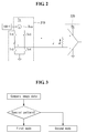
- FIG. 2 illustrates configuration of a data transmission device according to the embodiment of the invention.
- the data transmission device according to the embodiment of the invention uses the LVDS interface.
- the data transmission device includes the differential signaling driver 210, a current controller 100-1, and a receiving unit 220.
- the differential signaling driver 210 includes a variable current source Iva and first to fourth switching elements Tr1 to Tr4.
- the variable current source Iva provides a current corresponding to a control signal received from the current controller 100-1 for a circuit.
- the first switching element Tr1 and the fourth switching element Tr4 are turned on in response to a first input signal, and the second switching element Tr2 and the third switching element Tr3 are turned on in response to a second input signal.
- Each of the first to fourth switching elements Tr1 to Tr4 forms a current loop of a predetermined direction through its switching operation.
- the current controller 100-1 sets a current value the variable current source Iva of the differential signaling driver 210 outputs.
- the receiving unit 220 outputs a differential signal supplied through a pair of signal lines.
- FIG. 3 is a flow chart illustrating a method for setting a loop current according to the embodiment of the invention. The method for setting the loop current according to the embodiment of the invention is described below with reference to FIG. 3 .
- the current controller 100-1 decides toggling of image data. For example, the current controller 100-1 divides the image data into unit data of 8 bits and decides a toggling degree of each unit data.
- the toggling of the image data means the frequency of change in the image data divided into high data or low data.
- the current controller 100-1 selects a first mode and a second mode depending on the toggling of the image data.
- the current controller 100-1 When the toggling of the image data is low (for example, when a full black image or a full white image is displayed), the current controller 100-1 outputs a first control signal controlling an operation of the first mode.
- the current controller 100-1 may decide the toggling of the image data based on image data belonging to upper bits in a process for deciding the toggling of the image data. In such a process, the current controller 100-1 may decide the toggling of the image data based on image data belonging to six upper bits while ignoring image data belonging to two lower bits.
- the current controller 100-1 may decide the toggling of the image data based on only the image data belonging to the six upper bits. In particular, as shown in FIG. 4 , the current controller 100-1 may output the first control signal when red image data, green image data, and blue image data have the same upper bits, preferably the same six upper bits.
- the current controller 100-1 outputs a second control signal controlling an operation of the second mode except that the current controller 100-1 outputs the first control signal. For example, when different data is detected from image data belonging to six upper bits, the current controller 100-1 outputs the second control signal. In particular, as shown in FIG. 5 , the current controller 100-1 may output the second control signal when different data is detected from six upper bits of each of red image data, green image data, and blue image data.
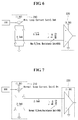
- the differential signaling driver 210 sets a current value of the variable current source Iva in response to the control signal received from the current controller 100-1. As shown in FIG. 6 , when the differential signaling driver 210 receives the first control signal, the differential signaling driver 210 selects a current value smaller than a current value selected when receiving the second control signal. For example, when the differential signaling driver 210 receives the first control signal, the differential signaling driver 210 may select the current of 0.5 mA as a loop current. As shown in FIG. 7 , when the differential signaling driver 210 receives the second control signal, the differential signaling driver 210 may select the current of 2.0 mA as a loop current.
- the differential signaling driver 210 selects the loop current in response to the first control signal or the second control signal and thus can prevent a reduction in transmission quality of the image data while reducing power consumption.
- the transmission reliability of the image data is proportional to the loop current. Because the transmission reliability of the image data is improved as the loop current increases, the current controller 100-1 controls the variable current source Iva so that the variable current source Iva selects the larger current value when the toggling of the image data is high.
- the current controller 100-1 controls the variable current source Iva so that the variable current source Iva selects the smaller current value.
- the current controller 100-1 selects a small value of the loop current focusing on a reduction in the power consumption.
- the receiving unit 220 varies a terminating resistance Rterm depending on the loop current. Since the loop current varies, a differential voltage is uniformly maintained at a predetermined value. When the differential voltage is uniformly maintained at 200 mV, the terminating resistance Rterm may be selected as follows. When the loop current is 0.5 mA in response to the first control signal, the receiving unit 220 sets the terminating resistance Rterm to 400 ⁇ . When the loop current is 2.0 mA in response to the second control signal, the receiving unit 220 sets the terminating resistance Rterm to 100 ⁇ .
- the current controller 100-1 outputs the first control signal and the second control signal and the differential signaling driver 210 controls a variable current based on the first control signal and the second control signal.
- the loop current of the differential signaling driver 210 may be selected depending on an optional signal.
- Table 1 shows an example of the loop current the differential signaling driver 210 sets depending on the optional signal.
- variable current source Iva of the differential signaling driver 210 may select one of a total of eight optional signals using the control signal received from the current controller 100-1.
- FIGS. 8 and 9 illustrate configuration of the source driver IC according to the embodiment of the invention.
- the source driver IC SIC includes a shift register 810, a latch 820, a digital-to-analog converter (DAC) 830, and an output buffer 840.
- Theshift register 810 samples bits of RGB digital video data of an input image in response to data control signals SSC and SSP received from the timing controller TCON and supplies them to the latch 820.
- the latch 820 samples and latches the bits of the RGB digital video data in response to a clock sequentially received from the shift register 810. Then, the latch 820 simultaneously outputs the latched RGB digital video data.
- the latch 820 simultaneously outputs the latched data in response to a source output enable signal SOE in synchronization with the latches 820 of other source driver ICs.
- the DAC 830 converts the image data into an analog data voltage using a gamma reference voltage Gamma received through a gamma buffer 851.
- the output unit 840 supplies the analog data voltage output from the DAC 830 to the data lines DL during a low logic period of the source output enable signal SOE.
- the output unit 840 outputs the data voltage using a low potential voltage GND and a voltage received through a driving voltage output buffer 852.
- a current controller 100-2, 100-1 reads the image data and varies a bias current supplied to the output buffer 840, the gamma buffer 851, and the driving voltage output buffer 852 of the source driver IC SIC.
- the driving voltage output buffer 852 includes a switching circuit unit 910 and buffer 852-1.
- the current controller 100-2 varies a bias current supplied to the switching circuit unit 910 of the driving voltage output buffer 852.
- the switching circuit unit 910 includes a plurality of switching elements SW1 to SW8 arranged in parallel between an input node nIN connected to a current source (not shown) and an output node nout connected to the driving voltage output buffer 852.
- the switching circuit unit 910 may select the number of switching elements connecting the input node nIN and the output node nout and may adjust a current value.
- the current controller 100-2 reads the image data. When an amount of change in the data voltage supplied to the same data line is equal to or less than a critical value, the current controller 100-2 controls an amount of the bias current of at least one of the output buffer 840, the gamma buffer 851, and the driving voltage output buffer 852, preferably the bias current of all three is controlled.
- the current controller 100-2 reads the image data on a per line basis. For example, the current controller 100-2 compares data of a first (data) line supplied during a first horizontal period 1H with data of a second (data) line supplied during a second horizontal period 2H. The current controller 100-2 compares the image data with respect to bits of the same location (i.e., the same order). When an amount of change in the image data belonging to the same location is equal to or less than a critical value, the current controller 100-2 varies the bias current.
- the critical value may be determined depending on the driving reliability and the power consumption. Even when the critical value is large and the amount of change in the image data is much, the bias current varies. Therefore, the driving reliability of the buffers is reduced. When the critical value is small, the driving reliability of the buffers increases. However, a reduction effect of the power consumption is reduced.
- FIG. 10 illustrates an example where the current controller 100-2 reads image data and varies the bias current.
- FIG. 10 illustrates an amount of change in data during a first period t1, in which there is a large change in the data voltage.
- the current controller 100-2 does not vary the bias current of the buffers during the first period t1.
- the current controller 100-2 may set the bias current of the buffers to a minimum value Min.Bias during the second period t2 and the third period t3. Subsequently, the current controller 100-2 does not vary the bias current of the buffers during a fourth period t4 in which there is a large change in the data voltage.
Landscapes
- Engineering & Computer Science (AREA)
- Physics & Mathematics (AREA)
- Computer Hardware Design (AREA)
- General Physics & Mathematics (AREA)
- Theoretical Computer Science (AREA)
- Chemical & Material Sciences (AREA)
- Crystallography & Structural Chemistry (AREA)
- Control Of Indicators Other Than Cathode Ray Tubes (AREA)
- Liquid Crystal Display Device Control (AREA)
Abstract
Description
- Embodiments of the invention relate to a display device and to method for operating a display device.
- Examples of a flat panel display include a liquid crystal display (LCD), a field emission display (FED), a plasma display panel (PDP), and an organic light emitting diode (OLED) display. In the flat panel display, data lines and gate lines are arranged to cross each other, and each crossing of the data lines and the gate lines is defined as a pixel. The plurality of pixels are formed on a display panel of the flat panel display in a matrix form. The flat panel display supplies a video data voltage to the data lines and sequentially supplies a gate pulse to the gate lines, thereby driving the pixels. The flat panel display supplies the video data voltage to the pixels of a gate line, to which the gate pulse is supplied, and sequentially scans all of the gate lines through the gate pulse, thereby displaying video data.
- A timing controller of a display device supplies digital video data, a clock for sampling the digital video data, a control signal for controlling operations of source driver integrated circuits (ICs), etc. to the source driver ICs through an interface such as low-voltage differential signaling (LVDS). The source driver ICs convert the digital video data serially received from the timing controller into parallel data and then convert the parallel data into an analog data voltage using a gamma compensation voltage. The source driver ICs supply the analog data voltages to the data lines, respectively. The LVDS interface method produces a differential signal using a current output from a current source of a differential signaling driver. However, the LVDS interface method increases power consumption in a process for increasing reliability of data transmission.
- Further, a data driver of the display device includes various buffers. Because a bias current of each buffer is fixed to a predetermined value, the data driver uses more than necessary consumption current.
- The object is solved by the features of the independent claims.
- A main idea of the invention is to analyze the input image data and to control the amount of current used for driving the data lines based on this analysis.
- In one aspect of the invention a display device comprising a display panel including data lines; a data driver configured to produce a data voltage corresponding to input image data and supply the data voltage to the data lines; and a current controller configured to determine an amount of change in the input image data and to control a current used in the data driver to drive the data lines based on the amount of change in the image data.
- Preferably, the display device comprises a differential signaling driver configured to produce a differential signal using a variable current; first and second signal lines configured to maintain a loop current in response to a signal output by the differential signaling driver; wherein the current controller is configured to reduce the variable current when one of low data and high data of image data is equal to or greater than a critical value; and a receiving unit configured to receive the differential signal through the first and second signal lines.
- Preferably, the current controller may divide the image data into unit data of a predetermined number of bits and may reduce the variable current when a further predetermined number of data or more bits is the same in any one unit data among the unit data.
- Preferably, the current controller is adapted to divide the image data into unit data of 8 bits and to reduce the variable current when unit data has the same six or more bits upper bits.
- Preferably, the current controller may divide each of red image data, green image data, and blue image data into unit data of 8 bits and to reduce the variable current when the red image data, the green image data, and the blue image data have the same six upper bits.
- Preferably, the receiving unit may set a terminating resistance depending on the loop current.
- Preferably, a terminating resistor may be positioned between the first and second signal lines, wherein the current controller may adjust a resistance of the terminating resistor so that the resistance of the terminating resistor is inversely proportional to the variable current.
- Preferably, the data driver is configured to produce a data voltage corresponding to input image data and to supply the data voltage to the data lines through an output buffer; wherein another current controller is configured to calculate an amount of change in the image data in the same channel and to vary a bias current of the output buffer based on the amount of change in the image data. The one and another current controller could be the same or separate current controllers.
- Preferably, the current controller may perform an operation reducing the bias current of the output buffer as the amount of change in the image data decreases.
- Preferably, the data driver may receive a gamma reference voltage through a gamma buffer so as to convert the image data into the data voltage, wherein the current controller is adapted to perform an operation reducing a bias current of the gamma buffer as the amount of change in the image data decreases.
- Preferably, the data driver may receive a high potential voltage through a driving voltage output buffer, wherein the current controller may perform an operation reducing a bias current of the driving voltage output buffer as the amount of change in the image data decreases.
- Preferably, the display device may comprise at least one source driver IC (SIC) including: a shift register, a latch, a digital-to-analog converter, and an output buffer.
- In another aspect of the invention a method is provided for operating a display device, comprising the steps of: receiving input image data, analyzing the image data, determining toggling of the image data or amount of change of input image data, controlling a current for driving based on the determined toggling of the image data or amount of change of input data.
- Preferably, the method further comprises the step of: if toggling of image data is lower than a critical value output a first control signal, or if toggling of image data is higher than a critical value output a second control signal, setting a loop current of a differential signaling driver of the display device based on the first or second control signal.
- Preferably, the method further comprises the step of: producing a data voltage corresponding to input image data, and calculating an amount of change in the image data in the same channel and varying a bias current of an output buffer based on the amount of change in the image data, supplying the data voltage to the data lines through an output buffer.
- In another aspect, there is a display device comprising a differential signaling driver configured to produce a differential signal using a variable current, first and second signal lines configured to maintain a loop current in response to a signal output by the differential signaling driver, a current controller configured to reduce the variable current when one of low data and high data of image data is equal to or greater than a critical value, and a receiving unit configured to receive the differential signal through the first and second signal lines.
- In another aspect, there is a display device comprising a display panel including data lines, a data driver configured to produce a data voltage corresponding to input image data and supply the data voltage to the data lines through an output buffer, and a current controller configured to calculate an amount of change in the image data in the same channel and vary a bias current of the output buffer based on the amount of change in the image data.
- The accompanying drawings, which are included to provide a further understanding of the invention and are incorporated in and constitute a part of this specification, illustrate embodiments of the invention and together with the description serve to explain the principles of the invention. In the drawings:
-
FIG. 1 illustrates a display device according to an exemplary embodiment of the invention; -
FIG. 2 illustrates a data transmission device according to an exemplary embodiment of the invention; -
FIG. 3 is a flow chart illustrating a current control method according to an exemplary embodiment of the invention; -
FIGS. 4 and 5 illustrate a method for deciding image data according to a first embodiment of the invention; -
FIGS. 6 and 7 illustrate a current control method according to a first embodiment of the invention; -
FIGS. 8 and9 illustrate configuration of a source driver integrated circuit (IC) according to an exemplary embodiment of the invention; and -
FIG. 10 illustrates a method for deciding image data according to a second embodiment of the invention. - Reference will now be made in detail to embodiments of the invention, examples of which are illustrated in the accompanying drawings. Wherever possible, the same reference numbers will be used throughout the drawings to refer to the same or like parts. It will be paid attention that detailed description of known arts will be omitted if it is determined that the arts can mislead the embodiments of the invention.
- Referring to
FIG. 1 , a liquid crystal display according to an exemplary embodiment of the invention includes a liquid crystal display panel LCP, a timing controller TCON, source driver integrated circuits (ICs)SIC# 1 toSIC# 8, and gate driver ICs GIC. - A liquid crystal layer is formed between substrates of the liquid crystal display panel LCP. The liquid crystal display panel LCP includes liquid crystal cells Clc arranged in a matrix form based on a crossing structure of data lines DL and gate lines GL.
- A pixel array including the data lines DL, the gate lines GL, thin film transistors (TFTs), storage capacitors Cst, etc. is formed on a TFT array substrate of the liquid crystal display panel LCP. Each liquid crystal cell Clc is driven by an electric field between a pixel electrode, to which a data voltage is supplied through the TFT, and a common electrode, to which a common voltage Vcom is supplied. A gate electrode of the TFT is connected to the gate line GL, and a drain electrode of the TFT is connected to the data line DL. A source electrode of the TFT is connected to the pixel electrode of the liquid crystal cell Clc. The TFT is turned on in response to a gate pulse supplied through the gate line GL and supplies the data voltage from the data line DL to the pixel electrode of the liquid crystal cell Clc.
- Black matrixes, color filters, the common electrode, etc. are formed on a color filter substrate of the liquid crystal display panel LCP. Polarizing plates are respectively attached to the TFT array substrate and the color filter substrate of the liquid crystal display panel LCP. Alignment layers for setting a pre-tilt angle of liquid crystals are respectively formed on the TFT array substrate and the color filter substrate of the liquid crystal display panel LCP. A spacer may be formed between the TFT array substrate and the color filter substrate of the liquid crystal display panel LCP to keep cell gaps of the liquid crystal cells Clc constant.
- The timing controller TCON receives external timing signals, such as a vertical sync signal Vsync, a horizontal sync signal Hsync, an external data enable signal DE, and an external clock CLK, from an external host system (not shown) through an interface, such as a low-voltage differential signaling (LVDS) interface and a transition minimized differential signaling (TMDS) interface.
- A differential signaling driver of the timing controller TCON transmits the external clock CLK and RGB digital video data to the source driver
ICs SIC# 1 toSIC# 8 through pairs of data lines. The timing controller TCON generates control data as a differential signal and may transmit the differential signal to the source driverICs SIC# 1 toSIC# 8 through the pairs of data lines. The control data includes source control data for controlling output timing, a polarity, etc. of the data voltage output from the source driverICs SIC# 1 toSIC# 8. The control data may include gate control data for controlling operation timing of the gate driver ICs GIC. - The source driver
ICs SIC# 1 toSIC# 8 receive the external clock CLK, the RGB digital video data, and the control data through the pairs of data lines. The source driverICs SIC# 1 toSIC# 8 generate a frequency of the external clock CLK as internal clocks of {(the number of bits of RGB digital video data)×2} using a phase locked loop (PLL) or a delay locked loop (DLL). The source driverICs SIC# 1 toSIC# 8 sample the RGB digital video data based on the internal clocks and then convert the sampled data into parallel data. - The source driver
ICs SIC# 1 toSIC# 8 decode the control data input through the pairs of data lines using a code mapping method and recover the source control data and the gate control data. The source driverICs SIC# 1 toSIC# 8 convert the RGB digital video parallel data into positive and negative analog video data voltages in response to the recovered source control data and supply the data voltages to the data lines DL of the liquid crystal display panel LCP. The source driverICs SIC# 1 toSIC# 8 may transmit the gate control data to at least one of the gate driver ICs GIC. - The gate driver IC GIC sequentially supplies a gate pulse to the gate lines GL in response to the gate control data, that is received from the timing controller TCON or is received through the source driver
ICs SIC# 1 toSIC# 8. The gate control data includes a gate start pulse GSP, a gate shift clock GSC, a gate output enable signal GOE, and the like. The gate start pulse GSP controls a start horizontal line of a scan operation during one vertical period in which one screen is displayed. The gate shift clock GSC is a clock signal that is input to a shift resistor inside the gate driver IC GIC and sequentially shifts the gate start pulse GSP. The gate output enable signal GOE controls output timing of the gate driver IC GIC. -
FIG. 2 illustrates configuration of a data transmission device according to the embodiment of the invention. The data transmission device according to the embodiment of the invention uses the LVDS interface. - Referring to
FIG. 2 , the data transmission device according to the embodiment of the invention includes thedifferential signaling driver 210, a current controller 100-1, and a receivingunit 220. - The
differential signaling driver 210 includes a variable current source Iva and first to fourth switching elements Tr1 to Tr4. The variable current source Iva provides a current corresponding to a control signal received from the current controller 100-1 for a circuit. - The first switching element Tr1 and the fourth switching element Tr4 are turned on in response to a first input signal, and the second switching element Tr2 and the third switching element Tr3 are turned on in response to a second input signal. Each of the first to fourth switching elements Tr1 to Tr4 forms a current loop of a predetermined direction through its switching operation.
- The current controller 100-1 sets a current value the variable current source Iva of the
differential signaling driver 210 outputs. - The receiving
unit 220 outputs a differential signal supplied through a pair of signal lines. -
FIG. 3 is a flow chart illustrating a method for setting a loop current according to the embodiment of the invention. The method for setting the loop current according to the embodiment of the invention is described below with reference toFIG. 3 . - The current controller 100-1 decides toggling of image data. For example, the current controller 100-1 divides the image data into unit data of 8 bits and decides a toggling degree of each unit data. The toggling of the image data means the frequency of change in the image data divided into high data or low data.
- The current controller 100-1 selects a first mode and a second mode depending on the toggling of the image data. When the toggling of the image data is low (for example, when a full black image or a full white image is displayed), the current controller 100-1 outputs a first control signal controlling an operation of the first mode. The current controller 100-1 may decide the toggling of the image data based on image data belonging to upper bits in a process for deciding the toggling of the image data. In such a process, the current controller 100-1 may decide the toggling of the image data based on image data belonging to six upper bits while ignoring image data belonging to two lower bits. Because the image data belonging to the two lower bits displays data of very small size within a display range of the image data, visibility of an error may be very low even if the error occurs. Thus, the current controller 100-1 may decide the toggling of the image data based on only the image data belonging to the six upper bits. In particular, as shown in
FIG. 4 , the current controller 100-1 may output the first control signal when red image data, green image data, and blue image data have the same upper bits, preferably the same six upper bits. - The current controller 100-1 outputs a second control signal controlling an operation of the second mode except that the current controller 100-1 outputs the first control signal. For example, when different data is detected from image data belonging to six upper bits, the current controller 100-1 outputs the second control signal. In particular, as shown in
FIG. 5 , the current controller 100-1 may output the second control signal when different data is detected from six upper bits of each of red image data, green image data, and blue image data. - The
differential signaling driver 210 sets a current value of the variable current source Iva in response to the control signal received from the current controller 100-1. As shown inFIG. 6 , when thedifferential signaling driver 210 receives the first control signal, thedifferential signaling driver 210 selects a current value smaller than a current value selected when receiving the second control signal. For example, when thedifferential signaling driver 210 receives the first control signal, thedifferential signaling driver 210 may select the current of 0.5 mA as a loop current. As shown inFIG. 7 , when thedifferential signaling driver 210 receives the second control signal, thedifferential signaling driver 210 may select the current of 2.0 mA as a loop current. - The
differential signaling driver 210 selects the loop current in response to the first control signal or the second control signal and thus can prevent a reduction in transmission quality of the image data while reducing power consumption. The transmission reliability of the image data is proportional to the loop current. Because the transmission reliability of the image data is improved as the loop current increases, the current controller 100-1 controls the variable current source Iva so that the variable current source Iva selects the larger current value when the toggling of the image data is high. - When the loop current increases, the transmission reliability of the image data is improved. However, the power consumption increases. Thus, when the toggling of the image data is low, the current controller 100-1 controls the variable current source Iva so that the variable current source Iva selects the smaller current value. When the toggling of the image data is low, a transmission error may scarcely occur in a process for transmitting the image data. Therefore, the current controller 100-1 selects a small value of the loop current focusing on a reduction in the power consumption.
- The receiving
unit 220 varies a terminating resistance Rterm depending on the loop current. Since the loop current varies, a differential voltage is uniformly maintained at a predetermined value. When the differential voltage is uniformly maintained at 200 mV, the terminating resistance Rterm may be selected as follows. When the loop current is 0.5 mA in response to the first control signal, the receivingunit 220 sets the terminating resistance Rterm to 400 Ω. When the loop current is 2.0 mA in response to the second control signal, the receivingunit 220 sets the terminating resistance Rterm to 100 Ω. - The above embodiment of the invention described that the current controller 100-1 outputs the first control signal and the second control signal and the
differential signaling driver 210 controls a variable current based on the first control signal and the second control signal. - The loop current of the
differential signaling driver 210 may be selected depending on an optional signal. The following Table 1 shows an example of the loop current thedifferential signaling driver 210 sets depending on the optional signal.[Table 1] Optional Signal Loop Current Differential Voltage LLL 0 mA 0 mV LLH 0.5 mA 50 mV LHL 1.0 mA 100 mV LHH 1.5 mA 150 mV HLL 2.0 mA 200 mV HLH 2.5 mA 250 mV HHL 3.0 mA 300 mV HHH 3.5 mA 350 mV - The variable current source Iva of the
differential signaling driver 210 may select one of a total of eight optional signals using the control signal received from the current controller 100-1. -
FIGS. 8 and9 illustrate configuration of the source driver IC according to the embodiment of the invention. - Referring to
FIG. 8 , the source driver IC SIC includes ashift register 810, alatch 820, a digital-to-analog converter (DAC) 830, and anoutput buffer 840. Theshift register 810 samples bits of RGB digital video data of an input image in response to data control signals SSC and SSP received from the timing controller TCON and supplies them to thelatch 820. Thelatch 820 samples and latches the bits of the RGB digital video data in response to a clock sequentially received from theshift register 810. Then, thelatch 820 simultaneously outputs the latched RGB digital video data. Thelatch 820 simultaneously outputs the latched data in response to a source output enable signal SOE in synchronization with thelatches 820 of other source driver ICs. TheDAC 830 converts the image data into an analog data voltage using a gamma reference voltage Gamma received through agamma buffer 851. Theoutput unit 840 supplies the analog data voltage output from theDAC 830 to the data lines DL during a low logic period of the source output enable signal SOE. Theoutput unit 840 outputs the data voltage using a low potential voltage GND and a voltage received through a drivingvoltage output buffer 852. - A current controller 100-2, 100-1 reads the image data and varies a bias current supplied to the
output buffer 840, thegamma buffer 851, and the drivingvoltage output buffer 852 of the source driver IC SIC. For this, as For example, as shown inFIG. 9 , the drivingvoltage output buffer 852 includes aswitching circuit unit 910 and buffer 852-1. The current controller 100-2 varies a bias current supplied to theswitching circuit unit 910 of the drivingvoltage output buffer 852. The switchingcircuit unit 910 includes a plurality of switching elements SW1 to SW8 arranged in parallel between an input node nIN connected to a current source (not shown) and an output node nout connected to the driving voltage output buffer 852.The switchingcircuit unit 910 may select the number of switching elements connecting the input node nIN and the output node nout and may adjust a current value. - The current controller 100-2 reads the image data. When an amount of change in the data voltage supplied to the same data line is equal to or less than a critical value, the current controller 100-2 controls an amount of the bias current of at least one of the
output buffer 840, thegamma buffer 851, and the drivingvoltage output buffer 852, preferably the bias current of all three is controlled. - The current controller 100-2 reads the image data on a per line basis. For example, the current controller 100-2 compares data of a first (data) line supplied during a first horizontal period 1H with data of a second (data) line supplied during a second horizontal period 2H. The current controller 100-2 compares the image data with respect to bits of the same location (i.e., the same order). When an amount of change in the image data belonging to the same location is equal to or less than a critical value, the current controller 100-2 varies the bias current. The critical value may be determined depending on the driving reliability and the power consumption. Even when the critical value is large and the amount of change in the image data is much, the bias current varies. Therefore, the driving reliability of the buffers is reduced. When the critical value is small, the driving reliability of the buffers increases. However, a reduction effect of the power consumption is reduced.
-
FIG. 10 illustrates an example where the current controller 100-2 reads image data and varies the bias current. -
FIG. 10 illustrates an amount of change in data during a first period t1, in which there is a large change in the data voltage. Thus, the current controller 100-2 does not vary the bias current of the buffers during the first period t1. On the other hand, if the data voltage keeps constant during a second period t2 and a third period t3, the current controller 100-2 varies the bias current of the buffers during the second period t2 and the third period t3. For example, as shown inFIG. 10 , the current controller 100-2 may set the bias current of the buffers to a minimum value Min.Bias during the second period t2 and the third period t3. Subsequently, the current controller 100-2 does not vary the bias current of the buffers during a fourth period t4 in which there is a large change in the data voltage. - Although embodiments have been described with reference to a number of illustrative embodiments thereof, it should be understood that numerous other modifications and embodiments can be devised by those skilled in the art that will fall within the scope of the principles of this disclosure. More particularly, various variations and modifications are possible in the component parts and/or arrangements of the subject combination arrangement within the scope of the disclosure, the drawings and the appended claims. In addition to variations and modifications in the component parts and/or arrangements, alternative uses will also be apparent to those skilled in the art.
Claims (15)
- A display device comprising:a display panel including data lines (DL);a data driver configured to produce a data voltage corresponding to input image data and supply the data voltage to the data lines (DL); anda current controller (100-1, 100-2) configured to determine an amount of change in the input image data and to control a current used in the data driver to drive the data lines based on the amount of change in the image data.
- The display device as claimed in claim 1, comprising:a differential signaling driver (210) configured to produce a differential signal using a variable current;first and second signal lines configured to maintain a loop current in response to a signal output by the differential signaling driver (210);wherein the current controller (100-1) is configured to reduce the variable current when one of low data and high data of image data is equal to or greater than a critical value; anda receiving unit (220) configured to receive the differential signal through the first and second signal lines.
- The display device of claim 2, wherein the current controller (100-1) is adapted to divide the image data into unit data of a predetermined number of bits and is adapted to reduce the variable current when a further predetermined number of data or more bits is the same in any one unit data among the unit data.
- The display device of claim 3, wherein the current controller (100-1) is adapted to divide the image data into unit data of 8 bits and to reduce the variable current when unit data has the same six or more bits upper bits.
- The display device of claim 4, wherein the current controller (100-1) is adapted to divide each of red image data, green image data, and blue image data into unit data of 8 bits and to reduce the variable current when the red image data, the green image data, and the blue image data have the same six upper bits.
- The display device as claimed in any one of the preceding claims 2-5, wherein the receiving unit (220) is adapted to set a terminating resistance (Rterm) depending on the loop current.
- The display device as claimed in any one of the preceding claims 2-6, further comprising a terminating resistor (Rterm) positioned between the first and second signal lines,
wherein the current controller (100-1) is adapted to adjust a resistance of the terminating resistor (Rterm) so that the resistance of the terminating resistor is inversely proportional to the variable current. - The display device as claimed in claim 1, wherein comprising:the data driver is configured to produce a data voltage corresponding to input image data and to supply the data voltage to the data lines (DL) through an output buffer (840); andwherein another current controller (100-2) is configured to calculate an amount of change in the image data in the same channel and to vary a bias current of the output buffer (840) based on the amount of change in the image data.
- The display device of claim 8, wherein the current controller (100-2) is adapted to perform an operation reducing the bias current of the output buffer (840) as the amount of change in the image data decreases.
- The display device of claim 8 or 9, wherein the data driver is adapted to receive a gamma reference voltage through a gamma buffer (851) so as to convert the image data into the data voltage, wherein the current controller (100-2) is adapted to perform an operation reducing a bias current of the gamma buffer (851) as the amount of change in the image data decreases.
- The display device as claimed in one of the claims 8, 9 or 10, wherein the data driver is adapted to receive a high potential voltage through a driving voltage output buffer (840), wherein the current controller (100-2) is adapted to perform an operation reducing a bias current of the driving voltage output buffer (840) as the amount of change in the image data decreases.
- The display device as claimed in one of the claims 8 - 11, comprising at least one source driver IC (SIC) including:- a shift register (810),- a latch (820),- a digital-to-analog converter, DAC, (830), and- an output buffer (840).
- Method for operating a display device, comprising the steps of:- receiving input image data,- analyzing the image data,- determining toggling of the image data or amount of change of input image data,- controlling a current for driving based on the determined toggling of the image data or amount of change of input data.
- The method as claimed in claim 13, further comprising the steps of:- wherein if toggling of image data is lower than a critical value output a first control signal,- if toggling of image data is higher than a critical value output a second control signal,- setting a loop current of a differential signaling driver of the display device based on the first or second control signal.
- The method as claimed in claim 13 or 14, further comprising the steps of:producing a data voltage corresponding to input image data, andcalculating an amount of change in the image data in the same channel andvarying a bias current of an output buffer (840) based on the amount of change in the image data,supplying the data voltage to the data lines (DL) through an output buffer (840).
Applications Claiming Priority (1)
| Application Number | Priority Date | Filing Date | Title |
|---|---|---|---|
| KR1020140195705A KR102219091B1 (en) | 2014-12-31 | 2014-12-31 | Display Device |
Publications (2)
| Publication Number | Publication Date |
|---|---|
| EP3040973A1 true EP3040973A1 (en) | 2016-07-06 |
| EP3040973B1 EP3040973B1 (en) | 2023-09-06 |
Family
ID=55027512
Family Applications (1)
| Application Number | Title | Priority Date | Filing Date |
|---|---|---|---|
| EP15202889.0A Active EP3040973B1 (en) | 2014-12-31 | 2015-12-29 | Display device |
Country Status (4)
| Country | Link |
|---|---|
| US (1) | US10115349B2 (en) |
| EP (1) | EP3040973B1 (en) |
| KR (1) | KR102219091B1 (en) |
| CN (1) | CN105741731B (en) |
Families Citing this family (10)
| Publication number | Priority date | Publication date | Assignee | Title |
|---|---|---|---|---|
| CN106652907B (en) * | 2017-01-05 | 2019-02-05 | 上海天马有机发光显示技术有限公司 | Organic light-emitting display panel, organic light-emitting display device and pixel compensation method |
| JP6883469B2 (en) * | 2017-05-09 | 2021-06-09 | オリンパス株式会社 | Endoscope |
| KR102473522B1 (en) * | 2017-12-19 | 2022-12-01 | 엘지디스플레이 주식회사 | Display device and method of driving the same |
| CN112104355B (en) * | 2020-10-16 | 2025-01-28 | 深圳市爱协生科技股份有限公司 | A source buffer configurable bias circuit |
| CN112542122B (en) * | 2020-12-04 | 2022-09-09 | Tcl华星光电技术有限公司 | Display device driving method and display device |
| CN113593492B (en) * | 2021-07-15 | 2022-10-04 | Tcl华星光电技术有限公司 | Driving system and driving method of display panel |
| KR102918187B1 (en) | 2021-09-16 | 2026-01-28 | 삼성디스플레이 주식회사 | Display device and method of operating the display device |
| KR102915782B1 (en) * | 2021-12-24 | 2026-01-20 | 엘지디스플레이 주식회사 | Display apparatus |
| CN118280239A (en) * | 2022-12-29 | 2024-07-02 | 华为技术有限公司 | Display driving circuit and control method thereof, display module, and electronic device |
| KR20260028968A (en) * | 2024-08-23 | 2026-03-04 | 엘지디스플레이 주식회사 | Gamma voltage generating circuit and display device including the same |
Citations (3)
| Publication number | Priority date | Publication date | Assignee | Title |
|---|---|---|---|---|
| US20040036457A1 (en) * | 2002-06-24 | 2004-02-26 | Mitsubishi Denki Kabushiki Kaisha | Current supply circuit and display apparatus including the same |
| US20040242171A1 (en) * | 2003-05-29 | 2004-12-02 | Nec Electronics Corporation | Transmitter circuit, transmission circuit and driver unit |
| US20070132696A1 (en) * | 2005-12-13 | 2007-06-14 | Tpo Hong Kong Holding Limited | Display device and driving circuit for capacitance load thereof |
Family Cites Families (4)
| Publication number | Priority date | Publication date | Assignee | Title |
|---|---|---|---|---|
| JP4068317B2 (en) * | 2001-07-27 | 2008-03-26 | Necディスプレイソリューションズ株式会社 | Liquid crystal display |
| JP4526279B2 (en) * | 2003-05-27 | 2010-08-18 | 三菱電機株式会社 | Image display device and image display method |
| KR100790492B1 (en) | 2005-07-01 | 2008-01-02 | 삼성전자주식회사 | Source driver controlling slew rate and its driving method |
| KR101325435B1 (en) | 2008-12-23 | 2013-11-08 | 엘지디스플레이 주식회사 | Liquid crystal display |
-
2014
- 2014-12-31 KR KR1020140195705A patent/KR102219091B1/en active Active
-
2015
- 2015-11-18 CN CN201510796204.5A patent/CN105741731B/en active Active
- 2015-12-08 US US14/962,336 patent/US10115349B2/en active Active
- 2015-12-29 EP EP15202889.0A patent/EP3040973B1/en active Active
Patent Citations (3)
| Publication number | Priority date | Publication date | Assignee | Title |
|---|---|---|---|---|
| US20040036457A1 (en) * | 2002-06-24 | 2004-02-26 | Mitsubishi Denki Kabushiki Kaisha | Current supply circuit and display apparatus including the same |
| US20040242171A1 (en) * | 2003-05-29 | 2004-12-02 | Nec Electronics Corporation | Transmitter circuit, transmission circuit and driver unit |
| US20070132696A1 (en) * | 2005-12-13 | 2007-06-14 | Tpo Hong Kong Holding Limited | Display device and driving circuit for capacitance load thereof |
Also Published As
| Publication number | Publication date |
|---|---|
| KR102219091B1 (en) | 2021-02-24 |
| KR20160083557A (en) | 2016-07-12 |
| US20160189661A1 (en) | 2016-06-30 |
| US10115349B2 (en) | 2018-10-30 |
| CN105741731A (en) | 2016-07-06 |
| CN105741731B (en) | 2019-05-31 |
| EP3040973B1 (en) | 2023-09-06 |
Similar Documents
| Publication | Publication Date | Title |
|---|---|---|
| KR102756873B1 (en) | Display Device and Driving Method Thereof | |
| EP3040973B1 (en) | Display device | |
| US12417729B2 (en) | Power control circuit for display device | |
| CN102568413B (en) | Liquid crystal display and driving method thereof | |
| KR101654355B1 (en) | Source Driver, Display Device having the same and Method for driving thereof | |
| JP4918007B2 (en) | Method for manufacturing array substrate for liquid crystal display device | |
| US10417980B2 (en) | Liquid crystal display device and driving method thereof | |
| TWI413047B (en) | Video display driver with data enable learning | |
| CN101763831B (en) | Liquid crystal display and method of driving the same | |
| EP3040978A1 (en) | Display device | |
| KR101818247B1 (en) | Liquid crystal display device and method for driving thereof | |
| CN106257580A (en) | Display device and the method driving this display device | |
| US9978326B2 (en) | Liquid crystal display device and driving method thereof | |
| KR101765798B1 (en) | liquid crystal display device and method of driving the same | |
| US20090237340A1 (en) | Liquid crystal display module and display system including the same | |
| KR101341028B1 (en) | Display device | |
| CN115862561B (en) | Signal transmission method and device, source driver and electronic equipment | |
| KR20130131807A (en) | Luquid crystal display device and method for diriving thereof | |
| KR20130037490A (en) | Driving apparatus for image display device and method for driving the same | |
| KR20100047071A (en) | Liquid crystal display device | |
| KR20160078770A (en) | Liquid Crystal Display | |
| KR102560740B1 (en) | Liquid crystal display device | |
| KR101338984B1 (en) | Circuit for controlling common voltage in liquid crystal display and controlling method of the same | |
| KR20080062810A (en) | Data transmission device and liquid crystal display device using the same | |
| KR20120043278A (en) | Liquid crystal display and driving method thereof |
Legal Events
| Date | Code | Title | Description |
|---|---|---|---|
| PUAI | Public reference made under article 153(3) epc to a published international application that has entered the european phase |
Free format text: ORIGINAL CODE: 0009012 |
|
| 17P | Request for examination filed |
Effective date: 20151229 |
|
| AK | Designated contracting states |
Kind code of ref document: A1 Designated state(s): AL AT BE BG CH CY CZ DE DK EE ES FI FR GB GR HR HU IE IS IT LI LT LU LV MC MK MT NL NO PL PT RO RS SE SI SK SM TR |
|
| AX | Request for extension of the european patent |
Extension state: BA ME |
|
| RBV | Designated contracting states (corrected) |
Designated state(s): AL AT BE BG CH CY CZ DE DK EE ES FI FR GB GR HR HU IE IS IT LI LT LU LV MC MK MT NL NO PL PT RO RS SE SI SK SM TR |
|
| STAA | Information on the status of an ep patent application or granted ep patent |
Free format text: STATUS: EXAMINATION IS IN PROGRESS |
|
| 17Q | First examination report despatched |
Effective date: 20200824 |
|
| GRAP | Despatch of communication of intention to grant a patent |
Free format text: ORIGINAL CODE: EPIDOSNIGR1 |
|
| STAA | Information on the status of an ep patent application or granted ep patent |
Free format text: STATUS: GRANT OF PATENT IS INTENDED |
|
| INTG | Intention to grant announced |
Effective date: 20230301 |
|
| GRAJ | Information related to disapproval of communication of intention to grant by the applicant or resumption of examination proceedings by the epo deleted |
Free format text: ORIGINAL CODE: EPIDOSDIGR1 |
|
| STAA | Information on the status of an ep patent application or granted ep patent |
Free format text: STATUS: EXAMINATION IS IN PROGRESS |
|
| GRAP | Despatch of communication of intention to grant a patent |
Free format text: ORIGINAL CODE: EPIDOSNIGR1 |
|
| STAA | Information on the status of an ep patent application or granted ep patent |
Free format text: STATUS: GRANT OF PATENT IS INTENDED |
|
| GRAS | Grant fee paid |
Free format text: ORIGINAL CODE: EPIDOSNIGR3 |
|
| INTC | Intention to grant announced (deleted) | ||
| GRAA | (expected) grant |
Free format text: ORIGINAL CODE: 0009210 |
|
| STAA | Information on the status of an ep patent application or granted ep patent |
Free format text: STATUS: THE PATENT HAS BEEN GRANTED |
|
| INTG | Intention to grant announced |
Effective date: 20230712 |
|
| AK | Designated contracting states |
Kind code of ref document: B1 Designated state(s): AL AT BE BG CH CY CZ DE DK EE ES FI FR GB GR HR HU IE IS IT LI LT LU LV MC MK MT NL NO PL PT RO RS SE SI SK SM TR |
|
| REG | Reference to a national code |
Ref country code: GB Ref legal event code: FG4D |
|
| REG | Reference to a national code |
Ref country code: CH Ref legal event code: EP |
|
| REG | Reference to a national code |
Ref country code: IE Ref legal event code: FG4D |
|
| REG | Reference to a national code |
Ref country code: DE Ref legal event code: R096 Ref document number: 602015085536 Country of ref document: DE |
|
| REG | Reference to a national code |
Ref country code: LT Ref legal event code: MG9D |
|
| REG | Reference to a national code |
Ref country code: NL Ref legal event code: MP Effective date: 20230906 |
|
| PG25 | Lapsed in a contracting state [announced via postgrant information from national office to epo] |
Ref country code: GR Free format text: LAPSE BECAUSE OF FAILURE TO SUBMIT A TRANSLATION OF THE DESCRIPTION OR TO PAY THE FEE WITHIN THE PRESCRIBED TIME-LIMIT Effective date: 20231207 |
|
| REG | Reference to a national code |
Ref country code: DE Ref legal event code: R082 Ref document number: 602015085536 Country of ref document: DE Representative=s name: TER MEER STEINMEISTER & PARTNER PATENTANWAELTE, DE |
|
| PG25 | Lapsed in a contracting state [announced via postgrant information from national office to epo] |
Ref country code: SE Free format text: LAPSE BECAUSE OF FAILURE TO SUBMIT A TRANSLATION OF THE DESCRIPTION OR TO PAY THE FEE WITHIN THE PRESCRIBED TIME-LIMIT Effective date: 20230906 Ref country code: RS Free format text: LAPSE BECAUSE OF FAILURE TO SUBMIT A TRANSLATION OF THE DESCRIPTION OR TO PAY THE FEE WITHIN THE PRESCRIBED TIME-LIMIT Effective date: 20230906 Ref country code: NO Free format text: LAPSE BECAUSE OF FAILURE TO SUBMIT A TRANSLATION OF THE DESCRIPTION OR TO PAY THE FEE WITHIN THE PRESCRIBED TIME-LIMIT Effective date: 20231206 Ref country code: LV Free format text: LAPSE BECAUSE OF FAILURE TO SUBMIT A TRANSLATION OF THE DESCRIPTION OR TO PAY THE FEE WITHIN THE PRESCRIBED TIME-LIMIT Effective date: 20230906 Ref country code: LT Free format text: LAPSE BECAUSE OF FAILURE TO SUBMIT A TRANSLATION OF THE DESCRIPTION OR TO PAY THE FEE WITHIN THE PRESCRIBED TIME-LIMIT Effective date: 20230906 Ref country code: HR Free format text: LAPSE BECAUSE OF FAILURE TO SUBMIT A TRANSLATION OF THE DESCRIPTION OR TO PAY THE FEE WITHIN THE PRESCRIBED TIME-LIMIT Effective date: 20230906 Ref country code: GR Free format text: LAPSE BECAUSE OF FAILURE TO SUBMIT A TRANSLATION OF THE DESCRIPTION OR TO PAY THE FEE WITHIN THE PRESCRIBED TIME-LIMIT Effective date: 20231207 Ref country code: FI Free format text: LAPSE BECAUSE OF FAILURE TO SUBMIT A TRANSLATION OF THE DESCRIPTION OR TO PAY THE FEE WITHIN THE PRESCRIBED TIME-LIMIT Effective date: 20230906 |
|
| REG | Reference to a national code |
Ref country code: AT Ref legal event code: MK05 Ref document number: 1609612 Country of ref document: AT Kind code of ref document: T Effective date: 20230906 |
|
| PG25 | Lapsed in a contracting state [announced via postgrant information from national office to epo] |
Ref country code: NL Free format text: LAPSE BECAUSE OF FAILURE TO SUBMIT A TRANSLATION OF THE DESCRIPTION OR TO PAY THE FEE WITHIN THE PRESCRIBED TIME-LIMIT Effective date: 20230906 |
|
| PG25 | Lapsed in a contracting state [announced via postgrant information from national office to epo] |
Ref country code: IS Free format text: LAPSE BECAUSE OF FAILURE TO SUBMIT A TRANSLATION OF THE DESCRIPTION OR TO PAY THE FEE WITHIN THE PRESCRIBED TIME-LIMIT Effective date: 20240106 |
|
| PG25 | Lapsed in a contracting state [announced via postgrant information from national office to epo] |
Ref country code: AT Free format text: LAPSE BECAUSE OF FAILURE TO SUBMIT A TRANSLATION OF THE DESCRIPTION OR TO PAY THE FEE WITHIN THE PRESCRIBED TIME-LIMIT Effective date: 20230906 |
|
| PG25 | Lapsed in a contracting state [announced via postgrant information from national office to epo] |
Ref country code: ES Free format text: LAPSE BECAUSE OF FAILURE TO SUBMIT A TRANSLATION OF THE DESCRIPTION OR TO PAY THE FEE WITHIN THE PRESCRIBED TIME-LIMIT Effective date: 20230906 |
|
| PG25 | Lapsed in a contracting state [announced via postgrant information from national office to epo] |
Ref country code: SM Free format text: LAPSE BECAUSE OF FAILURE TO SUBMIT A TRANSLATION OF THE DESCRIPTION OR TO PAY THE FEE WITHIN THE PRESCRIBED TIME-LIMIT Effective date: 20230906 Ref country code: RO Free format text: LAPSE BECAUSE OF FAILURE TO SUBMIT A TRANSLATION OF THE DESCRIPTION OR TO PAY THE FEE WITHIN THE PRESCRIBED TIME-LIMIT Effective date: 20230906 Ref country code: IS Free format text: LAPSE BECAUSE OF FAILURE TO SUBMIT A TRANSLATION OF THE DESCRIPTION OR TO PAY THE FEE WITHIN THE PRESCRIBED TIME-LIMIT Effective date: 20240106 Ref country code: ES Free format text: LAPSE BECAUSE OF FAILURE TO SUBMIT A TRANSLATION OF THE DESCRIPTION OR TO PAY THE FEE WITHIN THE PRESCRIBED TIME-LIMIT Effective date: 20230906 Ref country code: EE Free format text: LAPSE BECAUSE OF FAILURE TO SUBMIT A TRANSLATION OF THE DESCRIPTION OR TO PAY THE FEE WITHIN THE PRESCRIBED TIME-LIMIT Effective date: 20230906 Ref country code: CZ Free format text: LAPSE BECAUSE OF FAILURE TO SUBMIT A TRANSLATION OF THE DESCRIPTION OR TO PAY THE FEE WITHIN THE PRESCRIBED TIME-LIMIT Effective date: 20230906 Ref country code: AT Free format text: LAPSE BECAUSE OF FAILURE TO SUBMIT A TRANSLATION OF THE DESCRIPTION OR TO PAY THE FEE WITHIN THE PRESCRIBED TIME-LIMIT Effective date: 20230906 Ref country code: SK Free format text: LAPSE BECAUSE OF FAILURE TO SUBMIT A TRANSLATION OF THE DESCRIPTION OR TO PAY THE FEE WITHIN THE PRESCRIBED TIME-LIMIT Effective date: 20230906 Ref country code: PT Free format text: LAPSE BECAUSE OF FAILURE TO SUBMIT A TRANSLATION OF THE DESCRIPTION OR TO PAY THE FEE WITHIN THE PRESCRIBED TIME-LIMIT Effective date: 20240108 |
|
| PG25 | Lapsed in a contracting state [announced via postgrant information from national office to epo] |
Ref country code: PL Free format text: LAPSE BECAUSE OF FAILURE TO SUBMIT A TRANSLATION OF THE DESCRIPTION OR TO PAY THE FEE WITHIN THE PRESCRIBED TIME-LIMIT Effective date: 20230906 Ref country code: IT Free format text: LAPSE BECAUSE OF FAILURE TO SUBMIT A TRANSLATION OF THE DESCRIPTION OR TO PAY THE FEE WITHIN THE PRESCRIBED TIME-LIMIT Effective date: 20230906 |
|
| REG | Reference to a national code |
Ref country code: DE Ref legal event code: R097 Ref document number: 602015085536 Country of ref document: DE |
|
| PG25 | Lapsed in a contracting state [announced via postgrant information from national office to epo] |
Ref country code: DK Free format text: LAPSE BECAUSE OF FAILURE TO SUBMIT A TRANSLATION OF THE DESCRIPTION OR TO PAY THE FEE WITHIN THE PRESCRIBED TIME-LIMIT Effective date: 20230906 |
|
| PLBE | No opposition filed within time limit |
Free format text: ORIGINAL CODE: 0009261 |
|
| STAA | Information on the status of an ep patent application or granted ep patent |
Free format text: STATUS: NO OPPOSITION FILED WITHIN TIME LIMIT |
|
| PG25 | Lapsed in a contracting state [announced via postgrant information from national office to epo] |
Ref country code: DK Free format text: LAPSE BECAUSE OF FAILURE TO SUBMIT A TRANSLATION OF THE DESCRIPTION OR TO PAY THE FEE WITHIN THE PRESCRIBED TIME-LIMIT Effective date: 20230906 Ref country code: SI Free format text: LAPSE BECAUSE OF FAILURE TO SUBMIT A TRANSLATION OF THE DESCRIPTION OR TO PAY THE FEE WITHIN THE PRESCRIBED TIME-LIMIT Effective date: 20230906 |
|
| REG | Reference to a national code |
Ref country code: CH Ref legal event code: PL |
|
| 26N | No opposition filed |
Effective date: 20240607 |
|
| PG25 | Lapsed in a contracting state [announced via postgrant information from national office to epo] |
Ref country code: LU Free format text: LAPSE BECAUSE OF NON-PAYMENT OF DUE FEES Effective date: 20231229 |
|
| PG25 | Lapsed in a contracting state [announced via postgrant information from national office to epo] |
Ref country code: MC Free format text: LAPSE BECAUSE OF FAILURE TO SUBMIT A TRANSLATION OF THE DESCRIPTION OR TO PAY THE FEE WITHIN THE PRESCRIBED TIME-LIMIT Effective date: 20230906 |
|
| REG | Reference to a national code |
Ref country code: BE Ref legal event code: MM Effective date: 20231231 |
|
| PG25 | Lapsed in a contracting state [announced via postgrant information from national office to epo] |
Ref country code: MC Free format text: LAPSE BECAUSE OF FAILURE TO SUBMIT A TRANSLATION OF THE DESCRIPTION OR TO PAY THE FEE WITHIN THE PRESCRIBED TIME-LIMIT Effective date: 20230906 Ref country code: LU Free format text: LAPSE BECAUSE OF NON-PAYMENT OF DUE FEES Effective date: 20231229 |
|
| REG | Reference to a national code |
Ref country code: IE Ref legal event code: MM4A |
|
| PG25 | Lapsed in a contracting state [announced via postgrant information from national office to epo] |
Ref country code: IE Free format text: LAPSE BECAUSE OF NON-PAYMENT OF DUE FEES Effective date: 20231229 |
|
| PG25 | Lapsed in a contracting state [announced via postgrant information from national office to epo] |
Ref country code: BE Free format text: LAPSE BECAUSE OF NON-PAYMENT OF DUE FEES Effective date: 20231231 |
|
| PG25 | Lapsed in a contracting state [announced via postgrant information from national office to epo] |
Ref country code: CH Free format text: LAPSE BECAUSE OF NON-PAYMENT OF DUE FEES Effective date: 20231231 |
|
| PG25 | Lapsed in a contracting state [announced via postgrant information from national office to epo] |
Ref country code: IE Free format text: LAPSE BECAUSE OF NON-PAYMENT OF DUE FEES Effective date: 20231229 Ref country code: CH Free format text: LAPSE BECAUSE OF NON-PAYMENT OF DUE FEES Effective date: 20231231 Ref country code: BE Free format text: LAPSE BECAUSE OF NON-PAYMENT OF DUE FEES Effective date: 20231231 |
|
| PG25 | Lapsed in a contracting state [announced via postgrant information from national office to epo] |
Ref country code: BG Free format text: LAPSE BECAUSE OF FAILURE TO SUBMIT A TRANSLATION OF THE DESCRIPTION OR TO PAY THE FEE WITHIN THE PRESCRIBED TIME-LIMIT Effective date: 20230906 |
|
| PG25 | Lapsed in a contracting state [announced via postgrant information from national office to epo] |
Ref country code: BG Free format text: LAPSE BECAUSE OF FAILURE TO SUBMIT A TRANSLATION OF THE DESCRIPTION OR TO PAY THE FEE WITHIN THE PRESCRIBED TIME-LIMIT Effective date: 20230906 |
|
| PG25 | Lapsed in a contracting state [announced via postgrant information from national office to epo] |
Ref country code: CY Free format text: LAPSE BECAUSE OF FAILURE TO SUBMIT A TRANSLATION OF THE DESCRIPTION OR TO PAY THE FEE WITHIN THE PRESCRIBED TIME-LIMIT; INVALID AB INITIO Effective date: 20151229 |
|
| PG25 | Lapsed in a contracting state [announced via postgrant information from national office to epo] |
Ref country code: HU Free format text: LAPSE BECAUSE OF FAILURE TO SUBMIT A TRANSLATION OF THE DESCRIPTION OR TO PAY THE FEE WITHIN THE PRESCRIBED TIME-LIMIT; INVALID AB INITIO Effective date: 20151229 |
|
| PG25 | Lapsed in a contracting state [announced via postgrant information from national office to epo] |
Ref country code: TR Free format text: LAPSE BECAUSE OF FAILURE TO SUBMIT A TRANSLATION OF THE DESCRIPTION OR TO PAY THE FEE WITHIN THE PRESCRIBED TIME-LIMIT Effective date: 20230906 |
|
| PGFP | Annual fee paid to national office [announced via postgrant information from national office to epo] |
Ref country code: DE Payment date: 20251020 Year of fee payment: 11 |
|
| PGFP | Annual fee paid to national office [announced via postgrant information from national office to epo] |
Ref country code: GB Payment date: 20251023 Year of fee payment: 11 |
|
| PGFP | Annual fee paid to national office [announced via postgrant information from national office to epo] |
Ref country code: FR Payment date: 20251021 Year of fee payment: 11 |