EP3038245B1 - Stromwandler - Google Patents
Stromwandler Download PDFInfo
- Publication number
- EP3038245B1 EP3038245B1 EP14837151.1A EP14837151A EP3038245B1 EP 3038245 B1 EP3038245 B1 EP 3038245B1 EP 14837151 A EP14837151 A EP 14837151A EP 3038245 B1 EP3038245 B1 EP 3038245B1
- Authority
- EP
- European Patent Office
- Prior art keywords
- capacitor
- circuit substrate
- forming body
- passage
- heat radiation
- Prior art date
- Legal status (The legal status is an assumption and is not a legal conclusion. Google has not performed a legal analysis and makes no representation as to the accuracy of the status listed.)
- Active
Links
Images


Classifications
-
- H—ELECTRICITY
- H05—ELECTRIC TECHNIQUES NOT OTHERWISE PROVIDED FOR
- H05K—PRINTED CIRCUITS; CASINGS OR CONSTRUCTIONAL DETAILS OF ELECTRIC APPARATUS; MANUFACTURE OF ASSEMBLAGES OF ELECTRICAL COMPONENTS
- H05K7/00—Constructional details common to different types of electric apparatus
- H05K7/20—Modifications to facilitate cooling, ventilating, or heating
- H05K7/2089—Modifications to facilitate cooling, ventilating, or heating for power electronics, e.g. for inverters for controlling motor
- H05K7/209—Heat transfer by conduction from internal heat source to heat radiating structure
-
- H—ELECTRICITY
- H02—GENERATION; CONVERSION OR DISTRIBUTION OF ELECTRIC POWER
- H02M—APPARATUS FOR CONVERSION BETWEEN AC AND AC, BETWEEN AC AND DC, OR BETWEEN DC AND DC, AND FOR USE WITH MAINS OR SIMILAR POWER SUPPLY SYSTEMS; CONVERSION OF DC OR AC INPUT POWER INTO SURGE OUTPUT POWER; CONTROL OR REGULATION THEREOF
- H02M7/00—Conversion of AC power input into DC power output; Conversion of DC power input into AC power output
- H02M7/003—Constructional details, e.g. physical layout, assembly, wiring or busbar connections
-
- H—ELECTRICITY
- H02—GENERATION; CONVERSION OR DISTRIBUTION OF ELECTRIC POWER
- H02M—APPARATUS FOR CONVERSION BETWEEN AC AND AC, BETWEEN AC AND DC, OR BETWEEN DC AND DC, AND FOR USE WITH MAINS OR SIMILAR POWER SUPPLY SYSTEMS; CONVERSION OF DC OR AC INPUT POWER INTO SURGE OUTPUT POWER; CONTROL OR REGULATION THEREOF
- H02M7/00—Conversion of AC power input into DC power output; Conversion of DC power input into AC power output
- H02M7/02—Conversion of AC power input into DC power output without possibility of reversal
- H02M7/04—Conversion of AC power input into DC power output without possibility of reversal by static converters
- H02M7/12—Conversion of AC power input into DC power output without possibility of reversal by static converters using discharge tubes with control electrode or semiconductor devices with control electrode
- H02M7/21—Conversion of AC power input into DC power output without possibility of reversal by static converters using discharge tubes with control electrode or semiconductor devices with control electrode using devices of a triode or transistor type requiring continuous application of a control signal
- H02M7/217—Conversion of AC power input into DC power output without possibility of reversal by static converters using discharge tubes with control electrode or semiconductor devices with control electrode using devices of a triode or transistor type requiring continuous application of a control signal using semiconductor devices only
-
- H—ELECTRICITY
- H05—ELECTRIC TECHNIQUES NOT OTHERWISE PROVIDED FOR
- H05K—PRINTED CIRCUITS; CASINGS OR CONSTRUCTIONAL DETAILS OF ELECTRIC APPARATUS; MANUFACTURE OF ASSEMBLAGES OF ELECTRICAL COMPONENTS
- H05K7/00—Constructional details common to different types of electric apparatus
- H05K7/20—Modifications to facilitate cooling, ventilating, or heating
- H05K7/20845—Modifications to facilitate cooling, ventilating, or heating for automotive electronic casings
- H05K7/20854—Heat transfer by conduction from internal heat source to heat radiating structure
-
- H—ELECTRICITY
- H05—ELECTRIC TECHNIQUES NOT OTHERWISE PROVIDED FOR
- H05K—PRINTED CIRCUITS; CASINGS OR CONSTRUCTIONAL DETAILS OF ELECTRIC APPARATUS; MANUFACTURE OF ASSEMBLAGES OF ELECTRICAL COMPONENTS
- H05K7/00—Constructional details common to different types of electric apparatus
- H05K7/20—Modifications to facilitate cooling, ventilating, or heating
- H05K7/2089—Modifications to facilitate cooling, ventilating, or heating for power electronics, e.g. for inverters for controlling motor
- H05K7/20927—Liquid coolant without phase change
-
- H—ELECTRICITY
- H10—SEMICONDUCTOR DEVICES; ELECTRIC SOLID-STATE DEVICES NOT OTHERWISE PROVIDED FOR
- H10W—GENERIC PACKAGES, INTERCONNECTIONS, CONNECTORS OR OTHER CONSTRUCTIONAL DETAILS OF DEVICES COVERED BY CLASS H10
- H10W40/00—Arrangements for thermal protection or thermal control
- H10W40/40—Arrangements for thermal protection or thermal control involving heat exchange by flowing fluids
- H10W40/47—Arrangements for thermal protection or thermal control involving heat exchange by flowing fluids by flowing liquids, e.g. forced water cooling
-
- H—ELECTRICITY
- H01—ELECTRIC ELEMENTS
- H01H—ELECTRIC SWITCHES; RELAYS; SELECTORS; EMERGENCY PROTECTIVE DEVICES
- H01H9/00—Details of switching devices, not covered by groups H01H1/00 - H01H7/00
- H01H9/52—Cooling of switch parts
-
- H—ELECTRICITY
- H10—SEMICONDUCTOR DEVICES; ELECTRIC SOLID-STATE DEVICES NOT OTHERWISE PROVIDED FOR
- H10W—GENERIC PACKAGES, INTERCONNECTIONS, CONNECTORS OR OTHER CONSTRUCTIONAL DETAILS OF DEVICES COVERED BY CLASS H10
- H10W72/00—Interconnections or connectors in packages
- H10W72/071—Connecting or disconnecting
- H10W72/073—Connecting or disconnecting of die-attach connectors
- H10W72/07351—Connecting or disconnecting of die-attach connectors characterised by changes in properties of the die-attach connectors during connecting
- H10W72/07354—Connecting or disconnecting of die-attach connectors characterised by changes in properties of the die-attach connectors during connecting changes in dispositions
-
- H—ELECTRICITY
- H10—SEMICONDUCTOR DEVICES; ELECTRIC SOLID-STATE DEVICES NOT OTHERWISE PROVIDED FOR
- H10W—GENERIC PACKAGES, INTERCONNECTIONS, CONNECTORS OR OTHER CONSTRUCTIONAL DETAILS OF DEVICES COVERED BY CLASS H10
- H10W72/00—Interconnections or connectors in packages
- H10W72/30—Die-attach connectors
- H10W72/341—Dispositions of die-attach connectors, e.g. layouts
- H10W72/347—Dispositions of multiple die-attach connectors
-
- H—ELECTRICITY
- H10—SEMICONDUCTOR DEVICES; ELECTRIC SOLID-STATE DEVICES NOT OTHERWISE PROVIDED FOR
- H10W—GENERIC PACKAGES, INTERCONNECTIONS, CONNECTORS OR OTHER CONSTRUCTIONAL DETAILS OF DEVICES COVERED BY CLASS H10
- H10W72/00—Interconnections or connectors in packages
- H10W72/30—Die-attach connectors
- H10W72/351—Materials of die-attach connectors
- H10W72/352—Materials of die-attach connectors comprising metals or metalloids, e.g. solders
-
- H—ELECTRICITY
- H10—SEMICONDUCTOR DEVICES; ELECTRIC SOLID-STATE DEVICES NOT OTHERWISE PROVIDED FOR
- H10W—GENERIC PACKAGES, INTERCONNECTIONS, CONNECTORS OR OTHER CONSTRUCTIONAL DETAILS OF DEVICES COVERED BY CLASS H10
- H10W90/00—Package configurations
-
- H—ELECTRICITY
- H10—SEMICONDUCTOR DEVICES; ELECTRIC SOLID-STATE DEVICES NOT OTHERWISE PROVIDED FOR
- H10W—GENERIC PACKAGES, INTERCONNECTIONS, CONNECTORS OR OTHER CONSTRUCTIONAL DETAILS OF DEVICES COVERED BY CLASS H10
- H10W90/00—Package configurations
- H10W90/701—Package configurations characterised by the relative positions of pads or connectors relative to package parts
- H10W90/731—Package configurations characterised by the relative positions of pads or connectors relative to package parts of die-attach connectors
- H10W90/736—Package configurations characterised by the relative positions of pads or connectors relative to package parts of die-attach connectors between a chip and a stacked lead frame, conducting package substrate or heat sink
Definitions
- the present invention relates to power converters for converting DC power to AC power or for converting AC power to DC power, and more especially, to a power converter used for a hybrid vehicle or an electric vehicle.
- PTL 1 describes a configuration where heat of a control element is transferred to a cooler via a heat conduction plate supporting the control element, a shelf receiving unit supporting the heat conduction plate, and a housing forming the shelf receiving unit.
- heat conduction plate supporting the control element
- shelf receiving unit supporting the heat conduction plate
- housing forming the shelf receiving unit.
- US2003/133267 discloses a terminal structure that provides interfacing with power electronics circuitry and external circuitry.
- the thermal support may receive one or more power electronic circuits.
- the support may aid in removing heat from the terminal structure and the circuits through fluid circulating through the support.
- the support may form a shield from both external EMI/RFI and from interference generated by operation of the power electronic circuits.
- Features may be provided to permit and enhance connection of the circuitry to external circuitry, such as improved terminal configurations.
- Modular units may be assembled that may be coupled to electronic circuitry via plug-in arrangements or through interface with a backplane or similar mounting and interconnecting structures.
- EP1919069 discloses a power converter in which first and second bases composing a coolant path structure are arranged at the middle stage of the power converter, and semiconductor modules and a capacitor are arranged on both surfaces of the coolant path structure, thus the cooling efficiency is improved. Furthermore, through-holes are formed in the first and second bases, and cables of DC and AC circuits are laid via the through-holes, thus miniaturization of the power converter is realized.
- a problem of the present invention is to improve cooling performance of a control circuit substrate.
- the present invention allows for improving cooling performance of a control circuit substrate.
- FIG. 1 is a system diagram where a power converter of the present invention is applied to a so-called hybrid vehicle that travels using both an internal engine and an electric motor.
- the power converter according to the present invention is applicable not only to a hybrid vehicle but also to a so-called electric vehicle that travels solely by an electric motor and is further usable as a power converter for driving an electric motor used for general industrial machines .
- the power converter applied to a hybrid vehicle is described.
- FIG. 1 is a diagram illustrating a control block of a hybrid vehicle.
- An internal engine EGN and a motor generator MG are power sources for generating travelling torque of the vehicle.
- the motor generator MG not only generates rotating torque but also has a function to convert mechanical energy (torque) applied to the motor generator MG from outside to power.
- the motor generator MG is, for example, a synchronous electric motor/generator or an induction motor/generator and thus operates as a motor or a generator depending on an operation method as aforementioned.
- An output side of the internal engine EGN is transferred to the motor generator MG via a power distribution mechanism TSM.
- Rotating torque from the power distribution mechanism TSM or rotating torque generated by the motor generator MG is transferred to wheels via a transmission TM and a differential gear DEF.
- An inverter circuit unit 140 is electrically connected to the battery 136 via a DC connector 138, thereby allowing transmission or reception of power between the battery 136 and the inverter circuit unit 140.
- the inverter circuit unit 140 When the motor generator MG is operated as an electric motor, the inverter circuit unit 140 generates AC power from DC power supplied from the battery 136 via the DC connector 138 and supplies the AC power to the motor generator MG via an AC terminal 188.
- a configuration including the motor generator MG and the inverter circuit unit 140 operates as an electric motor/generator unit.
- the electric motor/generator unit may operate as an electric motor or as a generator depending on an operation status or operate as one of those as appropriate. Note that, in the present embodiment, by causing the electric motor/generator unit to operate as the electric motor unit with power from the battery 136, the wheels can be driven solely by power from the motor generator MG. Furthermore, in the present embodiment, by causing the electric motor/generator unit to operate as the generator unit by power from the internal engine EGN or power from the wheels to generate power, the battery 136 can be charged.
- the power converter 200 includes a capacitor module 500 for filtering DC power supplied to the inverter circuit unit 140.
- the power converter 200 includes a connector 21 for communication such as receiving a command from a host control device or transmitting status data to the host control device.
- a control circuit unit 172 calculates a control amount of the motor generator MG based on the command input from the connector 21.
- the control circuit unit 172 further calculates whether to cause to operate as the electric motor or as the generator, generates a control pulse based on the calculation result, and supplies the control pulse to a driver circuit 174.
- the driver circuit 174 then generates a driving pulse for controlling the inverter circuit unit 140 based on the control pulse.
- IGBT insulated gate type bipolar transistor
- the inverter circuit unit 140 includes power semiconductor modules 300a to 300c each corresponding to each of three phases of U phase, V phase, and W phase of AC power for output.
- the power semiconductor modules 300a to 300c each has an upper arm and a lower arm with an IGBT 328 and a diode 156 operating as the upper arm and an IGBT 330 and a diode 166 operating as the lower arm.
- these three phases correspond to each phase of three phases of armature coils in the motor generator MG.
- AC power is output from an intermediate electrode 169, which is a central point of each IGBT 328 and each IGBT 330 of the power semiconductor modules 300a to 300c.
- the AC power is connected to an AC bus bar which is an AC power line to the motor generator MG through an AC terminal 159 and an AC connecter 188.
- a collector electrode 153 of the IGBT 328 of the upper arm is electrically connected to a positive side capacitor terminal 506 of the capacitor module 500 via a positive terminal 157 while an emitter electrode of the IGBT 330 of the lower arm is electrically connected to a negative side capacitor terminal 504 of the capacitor module 500 via a negative terminal 158.
- control circuit unit 172 receives a control command from the host control device via the connector 21 and generates and supply, to the driver circuit 174, a control pulse which is a control signal for controlling the IGBT 328 or IGBT 330 included the upper arm or lower arm of the power semiconductor modules 300a to 300c of each phase included in the inverter circuit unit 140 based on the control command.
- the driver circuit 174 then, based on the control pulse, supplies a driving pulse for controlling the IGBT 328 or IGBT 330 included the upper arm or lower arm of the power semiconductor modules 150 of each phase to the IGBT 328 or IGBT 330 of each phase.
- the IGBT 328 or IGBT 330 performs conduction or blockage based on the driving pulse from the driver circuit 174 and converts DC power supplied from the battery 136 to three-phase AC power. This converted power is supplied to the motor generator MG1.
- the IGBT 328 includes the collector electrode 153, a signaling emitter electrode 155, and a gate electrode 154. Also, the IGBT 330 includes a collector electrode 163, signaling emitter electrode 165, and a gate electrode 164.
- the diode 156 is electrically connected between the collector electrode 153 and the emitter electrode. Also, the diode 166 is electrically connected between the collector electrode 163 and the emitter electrode.
- MOSFET metal-oxide semiconductor field-effect transistor
- an IGBT is suitable for a relatively high DC voltage while a MOSFET is suitable for a relatively low DC voltage.
- the capacitor module 500 includes a plurality of positive side capacitor terminals 506, a plurality of negative side capacitor terminals 504, a positive side power supply terminal 509 and a negative side power supply terminal 508.
- a high-voltage DC power from the battery 136 is supplied to the positive side power supply terminal 509 or negative side power supply terminal 508 via the DC connector 138 and then supplied to the inverter circuit unit 140 through the plurality of positive side capacitor terminals 506 or the plurality of negative side capacitor terminals 504 of the capacitor module 500.
- DC power having been converted to from AC power by the inverter circuit unit 140 is supplied to the capacitor module 500 through the positive side capacitor terminal 506 or negative side capacitor terminal 504 and then supplied and charged to the battery 136 from the positive side power supply terminal 509 or negative side power supply terminal 508 via the DC connector 138.
- the control circuit unit 172 includes a microcomputer for arithmetic processing of a switching timing of the IGBT 328 and IGBT 330.
- Input information to the microcomputer includes a target torque value required for the motor generator MG, a current value supplied to the motor generator MG from the power semiconductor module 150 having the upper and lower arms, and a magnetic pole position of a rotator of the motor generator MG1.
- the target torque value is based on the command signal output from the host control device (not illustrated) and the current value is detected based on a detection signal from a current sensor.
- the magnetic pole position is detected based on a detection signal output from a rotating magnetic pole sensor (not illustrated) such as a resolver provided to the motor generator MG.
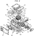
- FIG. 3 is an external view of the power converter 200.
- FIG. 4 is an external view of the power converter 200.
- a housing 400 is made from a metal, for example, an aluminum alloy and has a cuboid box shape having a pair of short side walls and long side walls.
- the housing 400 houses the capacitor module 500, power semiconductor modules 300a to 300c, control circuit unit 172, driver circuit 174, etc.
- the housing 400 includes a first long side wall 400A forming an opening for inserting the capacitor module 500 or the power semiconductor modules 300a to 300c or the like, a second long side wall 400B for fixing a lower cover 404, a first short side wall 400C for fixing a side cover 422, and a second short side wall 400D opposite to the first short side wall 400C.
- a pipe 406 is provided to the lower cover 404 and allows a coolant to flow in or flow out.
- a passage forming body 440 is disposed at a bottom part of the housing 400.
- the passage forming body 440 is formed integrally with the housing 400 by aluminum casting, resin molding, or the like.
- the capacitor module 500 is disposed at a storage part 402 provided at a side part of the passage forming body 440.
- a heat radiation sheet 407 is disposed between a lower wall of the storage part 402 and the capacitor module 500.
- the heat radiation sheet 407 has a heat radiation function of releasing the heat of the capacitor module 500 to the housing 400, lower cover 404, or passage forming body 440 and further has a function of insulating the housing 400, lower cover 404, or passage forming body 440.
- Three openings 403 are formed on a top surface of the passage forming body 440.
- the opening 403 communicates with the passage space (to be described later) in the passage forming body 440.
- Each of the power semiconductor modules 300a to 300c is inserted to the passage space from the three openings 403. Therefore, the power semiconductor modules 300a to 300c having a liquid-tight configuration themselves and the passage forming body 440 together seals the inside of the passage space is with a seal packing or the like. This results in a configuration where the power modules 300a to 300c are cooled by directly contacting the coolant.
- a DC side storage opening 409 and an AC side storage opening 410 are formed in a side wall 400E provided near the passage forming body 440.
- the DC terminal 408 is housed in the DC side storage opening 409.
- Three AC terminals 470 are housed in the AC side storage opening 410.
- Three AC connecting bus bars 416 connects the AC terminal 470 and each of the power semiconductor modules 300a to 300c.
- a current sensor 411 is disposed in a space between the power semiconductor modules 300a to 300c and the side wall 400E.
- a cooling board 413 is disposed in such a manner as to cover an upper part of the capacitor module 500, power semiconductor modules 300a to 300c, or current sensor 411.
- the cooling board 413 is fixed to the housing 400 and transfers heat to the housing 400.
- the cooling board 413 may be directly fixed to the passage forming body 440. This allows the cooling board 413 to release heat from the capacitor module 500 and heat from the AC connecting bus bar 416 to the passage forming body 440.
- a heat radiation sheet 415 is disposed between the capacitor module 500 and the cooling board 413 and releases heat of the capacitor module 500 to the cooling board 413.
- a heat radiation sheet 417 is disposed between the AC connecting bus bar 416 and the cooling board 413 and releases heat of the electric motor flowing in from the AC terminal 408 to the cooling board 413 via the AC connecting bus bar 416 and the heat radiation sheet 417.
- a driver circuit substrate 418 is disposed at an opposite side to the power semiconductor modules 300a to 300c across the cooling board 413.
- An upper cover 419 is fixed to the housing 400 with a housing fixing screw 420 in such a manner as to cover an opening of the first long side wall 400A.
- a control circuit substrate 421 is disposed at a side surface part 430 provided to the first short side wall 400C.
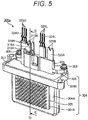
- FIG. 5 is a general perspective view of a power semiconductor module 300a.
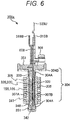
- FIG. 6 is a cross-sectional view of the power semiconductor module 300a according to the present embodiment cut along a cross section D and seen from a direction E. Any of the power semiconductor modules 300a to 300c has the same configuration.
- a configuration of the power semiconductor module 300a will be described as a typical example.
- a signal terminal 325U in FIG. 5 corresponds to the gate electrode 154 and the signaling emitter electrode 155 disclosed in FIG. 2 .
- a signal terminal 325L corresponds to the gate electrode 164 and the emitter electrode 165 disclosed in FIG. 2 .
- a DC positive terminal 315B is identical with the positive terminal 157 disclosed in FIG. 2 while the DC negative terminal 319B is identical with the negative terminal 158 disclosed in FIG. 2 .
- an AC terminal 320B is identical with the AC terminal 159 disclosed in FIG. 2 .
- the IGBT 328, IGBT 330, diode 156 and diode 166 are interposed between a conductor plate 341 and a conductor plate 342 and fixed to the conductor plate 341 and conductor plate 342 via solder.
- the IGBT 328, IGBT 330, diode 156 and diode 166 function as a power semiconductor element.
- a module case 304 is formed by a member having electrical conductivity, for example, by an aluminum alloy material (Al, AlSi, AlSiC, Al-C, etc.).
- An insertion opening 306 is formed on one surface of the module case 304 and receives the conductor plate 341, conductor plate 342, etc.
- a flange 304B is formed in such a manner as to encircle an outer periphery of the insertion opening 306.
- a first heat radiation surface 307A is disposed at a position opposite to a second heat radiation surface 307B via the IGBT 328, GBT 330, etc.
- the first heat radiation part 307A and second heat radiation surface 307B has a wider area than other areas of the module case 304, thereby improving heat radiation performance.
- Using a metal module case 304 in such a shape allows for preventing the coolant from entering inside the module case 304 with a simple configuration since sealing against the coolant can be ensured by a flange 304B even when the module case 304 is inserted inside a coolant passage 19 where the coolant such as water or oil flows.
- a fin 305 is formed in each of the first heat radiation part 307A and the second heat radiation part 307B.
- a thin part 304A is formed in an outer periphery of the first heat radiation surface 307A and second heat radiation surface 307B and is formed extremely thinner than the first heat radiation surface 307A and second heat radiation surface 307B.
- a thickness of the thin part 304A is made extremely thin to an extent that the thin part 304A is easily deformed by applying a pressure to the first heat radiation part 307A or second heat radiation part 307B. Therefore, productivity after the conductor plate 341 and conductor plate 342 are inserted is improved.
- the conductor plate 341 and conductor plate 342 are sealed with a first sealing resin 348 with a portion thereof being exposed.
- An exposed surface of the conductor plate 341 and conductor plate 342 is bonded with an insulating sheet 333 by thermocompression. This allows for reducing void space between a conductor plate 315 and an inner wall of the module case 304, thereby allowing for effective transfer of heat generated by the power semiconductor element to the fin 305.
- the insulating sheet 333 can absorb generated thermal stress. This is preferable for use in a power converter for vehicles with drastic temperature changes.
- a DC positive wiring 315A and a DC negative wiring 319A protrude from the insertion opening 306 and are electrically connected to the capacitor module 500.
- a DC positive terminal 315B (157) is formed at a tip of the DC positive wiring 315A.
- a DC negative terminal 319B (158) is formed at a tip of the DC negative wiring 319A.
- An AC wiring 320A protrudes from the insertion opening 306 and supplies AC power to the motor generator MG1 or MG2.
- An AC terminal 320B (159) is formed at a tip of the AC wiring 320A.
- a signal wiring 324U and a signal wiring 324L protrude from the insertion opening 306 and are electrically connected to the driver circuit 174.
- the signal terminal 325U (154, 155) and signal terminal 325L (164, 165) are formed at tips of the signal wiring 324U and signal wiring 324L.
- a wiring insulation part 608 is disposed between the DC positive wiring 315A and DC negative wiring 319A. This allows a current that instantaneously flows upon switching operation of the power semiconductor element to flow in an opposite direction. As a result, magnetic fields created by the current are canceled with each other. This action allows for reducing inductance.
- the AC wiring 320A or signal terminals 325U and 325L also extend in a direction similar to that of the DC positive wiring 315A and DC negative wiring 319A.
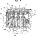
- FIG. 7 is a cross-sectional view of the power converter 200 cut along a plane A illustrated in FIG. 3 .
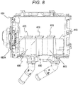
- FIG. 8 is a cross-sectional view of the power converter 200 in FIG. 7 , where components are removed, configured only by a passage forming body 400, an upper cover 419, and a side cover 422.
- the power semiconductor modules 300a to 300c are inserted from the opening 403 and disposed in the passage space 480 of the passage forming body 440. This allows the power semiconductor module to be disposed opposite to the passage space 480.
- the power semiconductor modules 300a to 300c are disposed inside the passage space 480, a plurality of passage pipes having a passage formed therein may be provided such that the power semiconductor modules 300a to 300c are interposed between the passage pipes.
- the driver circuit substrate 418 is disposed at a position opposite to a surface of the passage forming body 440 having the opening 403 formed thereon.
- the passage forming body 440 forms a side surface part 430 formed in parallel to an alignment direction of the power semiconductor module 300a and the driver circuit substrate 418.
- the side surface part 430 is formed integrally with the passage forming body 440.
- the side surface part 430 may be configured separately from the passage forming body 440 man be thermally connected to the passage forming body 440 through a heat radiation sheet or the like.
- a protruding portion 485A is formed on the side surface part 430 and protrudes toward the control circuit substrate 421. An edge of the protruding portion 485A is thermally in contact with the control circuit substrate 421.
- a heat radiation sheet or a heat radiation grease is disposed between the protruding portion 485A and the control circuit substrate 421.
- the power semiconductor module 300a is disposed in the passage space 480 such that a first passage space 481 is provided between one of inner walls of the passage space 480 illustrated in FIG. 8 and the first heat radiation part 307A of the power semiconductor module 300a and that a second passage space 482 is provided between another inner wall of the passage space 480 and the second heat radiation part 07B.
- the side surface part 430 is formed opposite to the power semiconductor module 300a across the first passage space 481.
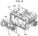
- FIG. 9 is an exploded perspective view of the power converter 200 where the side surface cover 422 is removed and a control circuit substrate 421 is disintegrated.
- a protruding portion 485B is formed on the side surface part 430 separately from the protruding portion 485A. This further improves heat radiation performance of the control circuit substrate 421.
- one of the protruding portion 485A and protruding portion 485B may not be included.
- a first storage space 471 is provided among a surface where the opening 403 of the passage forming body 440 is formed, an inner wall of the housing 400, and the upper cover 419.
- the driver circuit substrate 418 is disposed in the first storage space 470.
- a second storage space 472 is disposed between the side surface part 430 of the passage forming body 440 and the side surface cover 422.
- the control circuit substrate 421 is disposed in the second storage space 472.
- a wall 473 separates the first storage space 471 and the second storage space 472. As illustrated in FIG. 9 , an opening 474 is formed on the wall 473 such that the first storage space 471 is communicated with the second storage space 472.
- Wiring 490 runs through the opening 474 and electrically connects the driver circuit substrate 418 and the control circuit substrate 421. This allows for shielding the driver circuit substrate 418 against radiated electromagnetic noise with the wall 473, thereby protecting the control circuit substrate 421 from the electromagnetic noise.
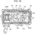
- FIG. 10 is a side view of the power converter 200, where the side surface cover 422 is removed, seen from a side where the control circuit substrate 421 is disposed.
- a projection 421S is a projection of the control circuit substrate 421 when a projection is made from a perpendicular direction to the side surface part 430.
- a projection 480S is a projection of the passage space 480 when a projection is made from a perpendicular direction to the side surface part 430.
- the control circuit substrate 421 is disposed on the side surface part 430 such that the projection 421S of the control circuit substrate 421 matches the projection 480S of the passage space 480 via the protruding portion 485A or protruding portion 485B protruding from the side surface part 430.
- a projection 485AS is a projection of the protruding portion 485A.
- a projection 485BS is a projection of the protruding portion 485B.
- the protruding portion 485A or protruding portion 485B is formed such that the projection 485AS or projection 485BS thereof matches the projection 421S of the control circuit substrate 421 and the projection 480S of the passage space 480. This allows for further improving cooling performance of the control circuit substrate 421.
- control circuit substrate 421 is disposed on, from among surfaces of the power converter 200, a surface different from a surface disposed with the driver circuit substrate 418. This allows the control circuit substrate 421 to be protected from electromagnetic noise generated from the driver circuit substrate 418.
- a metal plate or the like for electromagnetic shield which is disposed between the control circuit substrate 421 and the driver circuit substrate 418 is not required, thus allowing for downsizing and cost reduction with less number of parts.
- the protruding portion 485A and protruding portion 485B are formed integrally with the passage forming body 440 from a same material. This allows the protruding portion 485A and protruding portion 485B to be cooled by the coolant, thereby further improving cooling performance of the control circuit substrate 421.
- the control circuit substrate 421 has a first region 475 opposite to an opening surface of the opening 474. Furthermore, the control circuit substrate 421 is provided with a connecting part 476 connected to the wiring 490 at a position matching the first region 475. This allows for shortening the wiring 490 connecting the control circuit substrate 421 and driver circuit substrate 418, and thus much less electromagnetic noise from outside can affect the wiring 490. Also, shorter wiring 490 results in an effect of mitigating wiring impedance.
- the control circuit substrate 421 includes a microcomputer 173 for performing arithmetic operation for switching operation of the power semiconductor element.
- the microcomputer 173 is disposed such that a projection 173S of the microcomputer 173 matches the projection 480S of the passage space 480. This allows for effective cooling of the microcomputer 173 having a relatively high calorific value from among circuit parts mounted on the control circuit substrate 421.
- FIG. 11 is an external perspective view of a capacitor module 500 seen from a side where a capacitor terminal is formed.
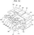
- FIG. 12 is an external perspective view of the capacitor module 500 illustrated in FIG. 11 , where the capacitor case 501 is removed.
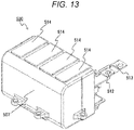
- FIG. 13 is an external perspective view of the capacitor module 500 seen from a side where the capacitor terminal is not formed.
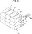
- FIG. 14 is an external perspective view of the capacitor module 500 illustrated in FIG. 13 , where the capacitor case 501 is removed.
- FIG. 15 is a cross-sectional view of the power converter 200 cut along a plane B in FIG. 3 .
- a capacitor element 501 filters DC power and supplies the DC power to the power semiconductor modules 300a to 300c.
- a positive side capacitor conductor plate 502 is connected to a positive side electrode of the capacitor element 501 via a lead terminal 504.
- a negative side capacitor conductor plate 503 is connected to a negative side electrode of the capacitor element 501 via a lead terminal (not illustrated).
- a noise-removing capacitor 508 has a smaller capacitance than the capacitor element 501 and filters ripple current caused by noise.
- a capacitor case 507 houses the capacitor element 501, positive side capacitor conductor plate 502, negative side capacitor conductor plate 503, and noise-removing capacitor 508.
- a sealing material 509 illustrated in FIG. 11 is filled to a storage space in the capacitor case 507.
- the capacitor case 507 has an opening 510 formed on a surface thereof.
- a conductor protruding portion 511 protrudes from the opening 510.
- Positive side capacitor terminals 505a to 505c and negative side capacitor terminals 506a to 506c bifurcate from the conductor protruding portion 511.
- the positive side capacitor terminal 505a is connected to the DC positive terminal 315B of the power semiconductor module 300a.
- the positive side capacitor terminal 505b is connected to the DC positive terminal 315B of the power semiconductor module 300b.
- the positive side capacitor terminal 505c is connected to the DC positive terminal 315B of the power semiconductor module 300c.
- the negative side capacitor terminal 506a is connected to the DC negative terminal 319B of the power semiconductor module 300a.
- the negative side capacitor terminal 506b is connected to the DC negative terminal 319B of the power semiconductor module 300b.
- the negative side capacitor terminal 506c is connected to the DC negative terminal 319B of the power semiconductor module 300c.
- a positive side power supply terminal 512 is connected to the positive side capacitor conductor plate 502 and protrudes from the opening 510.
- a negative side power supply terminal 513 is connected to the negative side capacitor conductor plate 503 and protrudes from the opening 510.
- the positive side capacitor conductor plate 502 has a conductor heat radiation part 514 protruding from the opening 510.
- the conductor heat radiation part 514 is thermally in contact with the passage forming body forming the passage space communicating with the pipe 406 via the heat radiation sheet 407 on a side of the passage. This allows for effectively radiating heat transferred from the positive side power supply terminal 512 or DC positive terminal 315B or heat transferred from the capacitor element 501.
- the capacitor case 507 is disposed in the passage forming body such that the opening 510 faces the power semiconductor modules 300a to 300c.
- the conductor heat radiation part 514 is formed along an outer wall of the capacitor case 507 such that the conductor heat radiation part 514 is disposed in a space between the capacitor case 507 and passage forming body.
- FIG. 16 is a general perspective view of the cooling board 413 seen from a side of a top surface.
- FIG. 17 is a general perspective view of the cooling board 413 seen from a side of a lower surface.
- the cooling board 413 has a heat receiving surface 600 thermally in contact with the conductor protruding portion 511 of the capacitor module 500 via the heat radiation sheet 415.
- the conductor protruding portion 511 is one plate and protrudes from the opening 510 and bifurcates into the positive side capacitor terminals 505a to 505c at an edge thereof.
- Such a configuration allows the conductor protruding portion 511 to be in contact with the heat receiving surface 600 of the cooling board 413 by a wide area, thereby improving cooling performance.
- a reflux circuit upon switching between the plurality of power semiconductor modules 300a to 300c flows in the conductor protruding portion 511. Therefore, causing this part to protrude from the opening 510 to be in contact with the cooling board 413 largely contributes improvement of cooling performance.
- a grounding terminal 520 illustrated in FIG. 11 is connected to the noise-removing capacitor 508.
- the grounding terminal 520 protrudes from the opening 510 from a side closer to the cooling board 413.
- the grounding terminal 520 protrudes from the opening 510 such that the grounding terminal 520 is disposed in a space between the conductor protruding portion 511 and the cooling board 413.
- a grounding connecting part 601 is formed in the cooling board 413 and is connected to the grounding terminal 520.
- the grounding connecting part 601 is formed at a position opposite to the grounding terminal 520.
- the cooling board 413 is connected to the metal housing 400. This allows the noise-removing capacitor 508 to be grounded via the cooling board 413, allowing the cooling board 413 to have both a heat radiation function and a grounding function. This contributes to a reduced number of parts or downsizing of the power converter 200.
Landscapes
- Engineering & Computer Science (AREA)
- Microelectronics & Electronic Packaging (AREA)
- Physics & Mathematics (AREA)
- Thermal Sciences (AREA)
- Power Engineering (AREA)
- Inverter Devices (AREA)
Claims (10)
- Leistungswandler (200), umfassend:ein Leistungshalbleitermodul (300a-300c), das ein Leistungshalbleiterelement (328, 330, 156, 166) aufweist, das konfiguriert ist, einen Gleichstrom in einen Wechselstrom umzuwandeln;einen Kanalausbildungskörper (440), der konfiguriert ist, einen Kanalraum (480) zu bilden, in dem ein Kühlmittel strömt;ein Treiberschaltungssubstrat (418), das konfiguriert ist, das Leistungshalbleiterelement (328, 330, 156, 166) anzusteuern; undein Steuerschaltungssubstrat (421), das konfiguriert ist, das Treiberschaltungssubstrat (418) zu steuern,wobei der Kanalausbildungskörper (440) eine erste Oberfläche und einen Seitenoberflächenteil (430) aufweist, der parallel zu einer zur ersten Oberfläche senkrechten Richtung ausgebildet ist,wobei das Treiberschaltungssubstrat (418) in einer der ersten Oberfläche gegenüberliegenden Position angeordnet ist,wobei das Steuerschaltungssubstrat (421) auf dem Seitenoberflächenteil (430) derart angeordnet ist, dass ein Vorsprung (421S) des Steuerschaltungssubstrats (421) dann, wenn ein Vorsprung (421S) des Steuerschaltungssubstrats (421) von einer zum Seitenoberflächenteil (430) senkrechten Richtung gefertigt ist, einen Vorsprung (480S) des Kanalraums (480) überlappt, wenn ein Vorsprung (480S) des Kanalraums (480) von der zum Seitenoberflächenteil (430) senkrechten Richtung gefertigt ist, undwobei das Steuerschaltungssubstrat (421) mit einem auf dem Seitenoberflächenteil (430) des Kanalausbildungskörpers (440) ausgebildeten, vorspringenden Abschnitt (485A, 485B) in thermischem Kontakt steht.
- Leistungswandler (200) gemäß Anspruch 1,
wobei der Kanalausbildungskörper (440) eine erste Öffnung bildet, um ein Anordnen des Leistungshalbleitermoduls (300a-300c) in einer dem Kanalraum (480) gegenüberliegenden Anordnung zu ermöglichen, und
wobei das Treiberschaltungssubstrat (418) in einer zu einer zur ersten Oberfläche des Kanalausbildungskörpers (440) gegenüberliegenden Position angeordnet ist, der die erste Öffnung auf derselben ausgebildet aufweist. - Leistungswandler (200) gemäß Anspruch 2,
wobei der Kanalausbildungskörper (440) derart ausgebildet ist, dass die erste Öffnung mit dem Kanalraum (480) kommuniziert,
wobei das Leistungshalbleitermodul (300a-300c) einen ersten Wärmeabstrahlungsteil (307A), der dem Leistungshalbleiterelement (328, 330, 156, 166) gegenüberliegt, und einen zweiten Wärmeabstrahlungsteil (307B), der einer ersten Wärmeabstrahlungsoberfläche auf der anderen Seite des Leistungshalbleiterelements (328, 330, 156, 166) gegenüberliegt, aufweist,
wobei das Leistungshalbleitermodul (300a-300c) ferner mit dem Kanalraum (480) derart angeordnet ist, dass ein erster Kanalraum (481) zwischen einer von Innenwänden des Kanalraums (480) und der ersten Wärmeabstrahlungsfläche ausgebildet ist, und dass ein zweiter Kanalraum (482) zwischen einer weiteren Innenwand des Kanalraums (480) und der zweiten Wärmeabstrahlungsfläche ausgebildet ist, und
wobei der Seitenoberflächenteil (430) dem Leistungshalbleitermodul (300a-300c) durch den ersten Kanalraum (481) hindurch gegenüberliegend ausgebildet ist. - Leistungswandler (200) gemäß Anspruch 2 oder 3,
wobei der vorspringende Abschnitt (485A, 485B) mit dem Kanalausbildungskörper (440) aus demselben Material einstückig geformt ist. - Leistungswandler (200) gemäß einem der Ansprüche 1 bis 4, umfassend:eine Verdrahtung (490), die konfiguriert ist, das Treiberschaltungssubstrat (418) und das Steuerschaltungssubstrat (421) elektrisch zu verbinden;ein Gehäuse (400), das konfiguriert ist, den Kanalausbildungskörper (440) aufzunehmen; undeine Abdeckung (419), die am Gehäuse (400) derart befestigt ist, dass der Seitenoberflächenteil (430) des Kanalausbildungskörpers (440) abgedeckt ist,wobei das Gehäuse (400) einen ersten Speicherraum (471), der zwischen einer Innenwand des Gehäuses (400) und der ersten Oberfläche des Kanalausbildungskörpers (440) vorgesehen ist, einen zweiten Speicherraum (472), der zwischen dem Seitenoberflächenteil (430) des Kanalausbildungskörpers (440) und der Abdeckung (419) vorgesehen ist, eine Wand, die den ersten Speicherraum (471) und den zweiten Speicherraum (472) trennt, und eine auf der Wand ausgebildete, zweite Öffnung bildet,wobei das Treiberschaltungssubstrat (418) im ersten Speicherraum (471) angeordnet ist,wobei das Steuerschaltungssubstrat (421) im zweiten Speicherraum (472) angeordnet ist, undwobei die Verdrahtung (490) das Treiberschaltungssubstrat (418) und das Steuerschaltungssubstrat (421) über die zweite Öffnung verbindet.
- Leistungswandler (200) gemäß Anspruch 5,
wobei das Steuerschaltungssubstrat (421) eine einer Öffnungsfläche der zweiten Öffnung gegenüberliegende, erste Region (475) aufweist, und
wobei die Verdrahtung (490) an einer Position verbunden ist, die der ersten Region (475) des Steuerschaltungssubstrats (421) entspricht. - Leistungswandler (200) gemäß einem der Ansprüche 1 bis 6,
wobei das Steuerschaltungssubstrat (421) einen Mikrocomputer (173) aufweist, der konfiguriert ist, eine arithmetische Operation zum Umschalten des Betriebs des Leistungshalbleiterelements (328, 330, 156, 166) auszuführen, und
wobei der Mikrocomputer (173) derart angeordnet ist, dass ein Vorsprung (173S) des Mikrocomputers (173) den Vorsprung (480S) des Kanalraums (480) überlappt. - Leistungswandler (200) gemäß einem der Ansprüche 1 bis 7, umfassend:ein Kondensatormodul (500), das konfiguriert ist, Gleichstromleistung zu filtern; undeine Kanalseiten-Wärmeabstrahlungsplatte, die im Kanalausbildungskörper (440) angeordnet ist,wobei das Kondensatormodul (500) ein Kondensatorelement (501), einen mit einer Elektrode des Kondensatorelements (501) elektrisch verbundenen Kondensatorseiten-Leiterteil und ein Kondensatorgehäuse (507), das konfiguriert ist, einen Teil des Kondensatorseiten-Leiterteils und das Kondensatorelement (501) aufzunehmen, umfasst, undwobei der Kondensatorseiten-Leiterteil von einer Öffnung des Kondensatorgehäuses (507) vorspringt, und einen Wärmeleiterabstrahlungsteil (514) aufweist, der in Kontakt mit der Kanalseiten-Wärmeabstrahlungsplatte steht.
- Leistungswandler (200) gemäß Anspruch 8,
wobei das Kondensatorgehäuse (507) im Kanalausbildungskörper (440) derart angeordnet ist, dass die Öffnung des Kondensatorgehäuses (507) dem Leistungshalbleitermodul (300a-300c) zugewandt ist, und
wobei der Wärmeleiterabstrahlungsteil (514) entlang einer Außenwand des Kondensatorgehäuses (507) derart ausgebildet ist, dass der Wärmeleiterabstrahlungsteil (514) in einem Raum zwischen dem Kondensatorgehäuse (507) und dem Kanalausbildungskörper (440) angeordnet ist. - Leistungswandler (200) gemäß einem der Ansprüche 1 bis 4, umfassend:ein Kondensatormodul (500), das zum Filtern von Gleichstromleistung konfiguriert ist;ein Gehäuse (400), das zum Aufnehmen des Kanalausbildungskörpers (440) konfiguriert ist;eine Metallkühlungsplatte (413), die zum elektrischen und thermischen In-Kontakt-Stehen mit dem Gehäuse (400) konfiguriert ist; undein Plattenseiten-Wärmeabstrahlungsblech (417), das mit der Metallkühlungsplatte (413) in Kontakt steht,wobei das Kondensatormodul (500) ein Kondensatorelement (501), einen mit einer Elektrode des Kondensatorelements (501) elektrisch verbundenen, ersten Kondensatorseiten-Leiterteil, ein rauschentfernendes Kondensatorelement (508), das eine kleinere elektrische Kapazität als das Kondensatorelement (501) aufweist, einen mit dem rauschentfernenden Kondensator (508) verbundenen Masseanschluss (520) und ein Kondensatorgehäuse (507), das zum Aufnehmen eines Teils des Kondensatorseiten-Leiterteils und des Kondensatorelements (501) konfiguriert ist, umfasst,wobei das Kondensatorgehäuse (507) im Kanalausbildungskörper (440) derart angeordnet ist, dass die Öffnung des Kondensatorgehäuses (507) dem Leistungshalbleitermodul (300a-300c) zugewandt ist,wobei der erste Kondensatorseiten-Leiterteil von der Öffnung des Kondensatorgehäuses (507) vorspringt und mit dem Plattenseiten-Wärmeabstrahlungsblech (417) in Kontakt steht, und ferner zu einer Ausrichtungsrichtung des Leistungshalbleitermoduls (300a-300c) hin ausgebildet ist, undwobei der Masseanschluss (520) von der Öffnung des Kondensatorgehäuses (507) vorspringt und mit der Metallkühlungsplatte (413) in Kontakt steht.
Applications Claiming Priority (2)
| Application Number | Priority Date | Filing Date | Title |
|---|---|---|---|
| JP2013170047 | 2013-08-20 | ||
| PCT/JP2014/065673 WO2015025594A1 (ja) | 2013-08-20 | 2014-06-13 | 電力変換装置 |
Publications (3)
| Publication Number | Publication Date |
|---|---|
| EP3038245A1 EP3038245A1 (de) | 2016-06-29 |
| EP3038245A4 EP3038245A4 (de) | 2017-05-03 |
| EP3038245B1 true EP3038245B1 (de) | 2018-11-14 |
Family
ID=52483379
Family Applications (1)
| Application Number | Title | Priority Date | Filing Date |
|---|---|---|---|
| EP14837151.1A Active EP3038245B1 (de) | 2013-08-20 | 2014-06-13 | Stromwandler |
Country Status (5)
| Country | Link |
|---|---|
| US (1) | US9717167B2 (de) |
| EP (1) | EP3038245B1 (de) |
| JP (1) | JP6117362B2 (de) |
| CN (1) | CN105474767B (de) |
| WO (1) | WO2015025594A1 (de) |
Families Citing this family (15)
| Publication number | Priority date | Publication date | Assignee | Title |
|---|---|---|---|---|
| DE102014111421A1 (de) * | 2014-08-11 | 2016-02-11 | Woodward Kempen Gmbh | Niederinduktive Schaltungsanordnung eines Umrichters |
| US10137798B2 (en) * | 2015-08-04 | 2018-11-27 | Ford Global Technologies, Llc | Busbars for a power module assembly |
| US10637345B2 (en) * | 2016-07-08 | 2020-04-28 | Mitsubishi Electric Corporation | Semiconductor device and power conversion device |
| DE112017005862B4 (de) * | 2016-12-22 | 2025-10-09 | Hitachi Astemo, Ltd. | Leistungsumsetzungsvorrichtung |
| CN110476343B (zh) * | 2017-04-14 | 2021-07-20 | 松下知识产权经营株式会社 | 电力转换装置 |
| IT201700070324A1 (it) * | 2017-06-23 | 2018-12-23 | Meta System Spa | Apparecchiatura elettronica di potenza per auto elettriche o ibride e relativo procedimento di realizzazione |
| US11239762B2 (en) * | 2017-11-02 | 2022-02-01 | Hitachi Astemo, Ltd. | Power converter |
| JP7065595B2 (ja) * | 2017-12-13 | 2022-05-12 | 株式会社Soken | フィルムコンデンサモジュール |
| WO2020211034A1 (zh) * | 2019-04-18 | 2020-10-22 | 威刚科技股份有限公司 | 控制器装置 |
| US10665398B1 (en) * | 2019-09-23 | 2020-05-26 | GM Global Technology Operations LLC | Direct current solid-state switch |
| CN110932529B (zh) * | 2019-12-17 | 2021-03-16 | 国网江苏省电力有限公司检修分公司 | 三电平功率模块装置 |
| JP7180631B2 (ja) * | 2020-03-27 | 2022-11-30 | 株式会社デンソー | コンデンサモジュールおよび電力変換装置 |
| JP7296336B2 (ja) * | 2020-03-27 | 2023-06-22 | 株式会社日立製作所 | 電力変換装置 |
| KR20220145653A (ko) * | 2021-04-22 | 2022-10-31 | 현대자동차주식회사 | 전력 변환 장치 |
| JP2024073864A (ja) * | 2022-11-18 | 2024-05-30 | 株式会社デンソー | コンデンサ装置 |
Family Cites Families (14)
| Publication number | Priority date | Publication date | Assignee | Title |
|---|---|---|---|---|
| JP2907753B2 (ja) | 1995-03-31 | 1999-06-21 | 株式会社三社電機製作所 | 電源装置 |
| TW283274B (de) | 1994-11-08 | 1996-08-11 | Sansha Denki Seisakusho Co Ltd | |
| JP4231626B2 (ja) | 1998-09-18 | 2009-03-04 | 株式会社日立製作所 | 自動車用モータ駆動装置 |
| US6898072B2 (en) * | 2002-01-16 | 2005-05-24 | Rockwell Automation Technologies, Inc. | Cooled electrical terminal assembly and device incorporating same |
| US7177153B2 (en) * | 2002-01-16 | 2007-02-13 | Rockwell Automation Technologies, Inc. | Vehicle drive module having improved cooling configuration |
| JP4848187B2 (ja) * | 2006-01-17 | 2011-12-28 | 日立オートモティブシステムズ株式会社 | 電力変換装置 |
| JP4751810B2 (ja) * | 2006-11-02 | 2011-08-17 | 日立オートモティブシステムズ株式会社 | 電力変換装置 |
| JP4994123B2 (ja) * | 2007-06-18 | 2012-08-08 | ニチコン株式会社 | パワー半導体モジュール |
| JP4452953B2 (ja) * | 2007-08-09 | 2010-04-21 | 日立オートモティブシステムズ株式会社 | 電力変換装置 |
| JP4797077B2 (ja) * | 2009-02-18 | 2011-10-19 | 株式会社日立製作所 | 半導体パワーモジュール、電力変換装置、および、半導体パワーモジュールの製造方法 |
| JP5481148B2 (ja) * | 2009-10-02 | 2014-04-23 | 日立オートモティブシステムズ株式会社 | 半導体装置、およびパワー半導体モジュール、およびパワー半導体モジュールを備えた電力変換装置 |
| CN103098363A (zh) * | 2010-09-30 | 2013-05-08 | 日立汽车系统株式会社 | 电力转换装置 |
| JP5647633B2 (ja) * | 2012-02-15 | 2015-01-07 | 日立オートモティブシステムズ株式会社 | 電力変換装置 |
| JP5738794B2 (ja) * | 2012-03-30 | 2015-06-24 | 日立オートモティブシステムズ株式会社 | 電力変換装置 |
-
2014
- 2014-06-13 US US14/902,365 patent/US9717167B2/en active Active
- 2014-06-13 EP EP14837151.1A patent/EP3038245B1/de active Active
- 2014-06-13 WO PCT/JP2014/065673 patent/WO2015025594A1/ja not_active Ceased
- 2014-06-13 CN CN201480045368.8A patent/CN105474767B/zh active Active
- 2014-06-13 JP JP2015532746A patent/JP6117362B2/ja active Active
Non-Patent Citations (1)
| Title |
|---|
| None * |
Also Published As
| Publication number | Publication date |
|---|---|
| US20160374229A1 (en) | 2016-12-22 |
| EP3038245A4 (de) | 2017-05-03 |
| WO2015025594A1 (ja) | 2015-02-26 |
| JPWO2015025594A1 (ja) | 2017-03-02 |
| US9717167B2 (en) | 2017-07-25 |
| CN105474767A (zh) | 2016-04-06 |
| CN105474767B (zh) | 2017-10-13 |
| JP6117362B2 (ja) | 2017-04-19 |
| EP3038245A1 (de) | 2016-06-29 |
Similar Documents
| Publication | Publication Date | Title |
|---|---|---|
| EP3038245B1 (de) | Stromwandler | |
| EP3493387B1 (de) | Wechselrichter | |
| CN103339847B (zh) | 车辆用电力变换装置 | |
| EP2288012B1 (de) | Stromkreisvorrichtung, Stromkreismodul und Stromwandler | |
| CN103299532B (zh) | 电力转换装置 | |
| CN103283137B (zh) | 电力转换装置 | |
| CN101534069B (zh) | 电力转换装置 | |
| CN103283138B (zh) | 电力转换装置 | |
| CN103703667B (zh) | 电力变换装置 | |
| EP2736160A1 (de) | Stromwandler | |
| EP2782433A2 (de) | Stromrichter | |
| EP2624432A1 (de) | Stromwandlervorrichtung | |
| JP6039356B2 (ja) | 電力変換装置 | |
| CN102197579A (zh) | 电力转换装置 | |
| JP4055643B2 (ja) | インバータ装置 | |
| JP2012253954A (ja) | 電力用変換装置 | |
| CN113574787B (zh) | 功率转换装置和功率转换装置的制造方法 |
Legal Events
| Date | Code | Title | Description |
|---|---|---|---|
| PUAI | Public reference made under article 153(3) epc to a published international application that has entered the european phase |
Free format text: ORIGINAL CODE: 0009012 |
|
| 17P | Request for examination filed |
Effective date: 20151222 |
|
| AK | Designated contracting states |
Kind code of ref document: A1 Designated state(s): AL AT BE BG CH CY CZ DE DK EE ES FI FR GB GR HR HU IE IS IT LI LT LU LV MC MK MT NL NO PL PT RO RS SE SI SK SM TR |
|
| AX | Request for extension of the european patent |
Extension state: BA ME |
|
| DAX | Request for extension of the european patent (deleted) | ||
| A4 | Supplementary search report drawn up and despatched |
Effective date: 20170330 |
|
| RIC1 | Information provided on ipc code assigned before grant |
Ipc: H05K 7/20 20060101ALI20170325BHEP Ipc: H02M 7/48 20070101AFI20170325BHEP |
|
| REG | Reference to a national code |
Ref country code: DE Ref legal event code: R079 Ref document number: 602014036185 Country of ref document: DE Free format text: PREVIOUS MAIN CLASS: H02M0007480000 Ipc: H05K0007200000 |
|
| GRAP | Despatch of communication of intention to grant a patent |
Free format text: ORIGINAL CODE: EPIDOSNIGR1 |
|
| STAA | Information on the status of an ep patent application or granted ep patent |
Free format text: STATUS: GRANT OF PATENT IS INTENDED |
|
| RIC1 | Information provided on ipc code assigned before grant |
Ipc: H05K 7/20 20060101AFI20180430BHEP Ipc: H02M 7/00 20060101ALI20180430BHEP Ipc: H02M 7/48 20070101ALI20180430BHEP |
|
| INTG | Intention to grant announced |
Effective date: 20180604 |
|
| GRAS | Grant fee paid |
Free format text: ORIGINAL CODE: EPIDOSNIGR3 |
|
| GRAA | (expected) grant |
Free format text: ORIGINAL CODE: 0009210 |
|
| STAA | Information on the status of an ep patent application or granted ep patent |
Free format text: STATUS: THE PATENT HAS BEEN GRANTED |
|
| AK | Designated contracting states |
Kind code of ref document: B1 Designated state(s): AL AT BE BG CH CY CZ DE DK EE ES FI FR GB GR HR HU IE IS IT LI LT LU LV MC MK MT NL NO PL PT RO RS SE SI SK SM TR |
|
| REG | Reference to a national code |
Ref country code: CH Ref legal event code: EP Ref country code: AT Ref legal event code: REF Ref document number: 1066399 Country of ref document: AT Kind code of ref document: T Effective date: 20181115 |
|
| REG | Reference to a national code |
Ref country code: DE Ref legal event code: R096 Ref document number: 602014036185 Country of ref document: DE |
|
| REG | Reference to a national code |
Ref country code: IE Ref legal event code: FG4D |
|
| REG | Reference to a national code |
Ref country code: NL Ref legal event code: MP Effective date: 20181114 |
|
| REG | Reference to a national code |
Ref country code: LT Ref legal event code: MG4D |
|
| REG | Reference to a national code |
Ref country code: AT Ref legal event code: MK05 Ref document number: 1066399 Country of ref document: AT Kind code of ref document: T Effective date: 20181114 |
|
| PG25 | Lapsed in a contracting state [announced via postgrant information from national office to epo] |
Ref country code: FI Free format text: LAPSE BECAUSE OF FAILURE TO SUBMIT A TRANSLATION OF THE DESCRIPTION OR TO PAY THE FEE WITHIN THE PRESCRIBED TIME-LIMIT Effective date: 20181114 Ref country code: BG Free format text: LAPSE BECAUSE OF FAILURE TO SUBMIT A TRANSLATION OF THE DESCRIPTION OR TO PAY THE FEE WITHIN THE PRESCRIBED TIME-LIMIT Effective date: 20190214 Ref country code: NO Free format text: LAPSE BECAUSE OF FAILURE TO SUBMIT A TRANSLATION OF THE DESCRIPTION OR TO PAY THE FEE WITHIN THE PRESCRIBED TIME-LIMIT Effective date: 20190214 Ref country code: LT Free format text: LAPSE BECAUSE OF FAILURE TO SUBMIT A TRANSLATION OF THE DESCRIPTION OR TO PAY THE FEE WITHIN THE PRESCRIBED TIME-LIMIT Effective date: 20181114 Ref country code: IS Free format text: LAPSE BECAUSE OF FAILURE TO SUBMIT A TRANSLATION OF THE DESCRIPTION OR TO PAY THE FEE WITHIN THE PRESCRIBED TIME-LIMIT Effective date: 20190314 Ref country code: LV Free format text: LAPSE BECAUSE OF FAILURE TO SUBMIT A TRANSLATION OF THE DESCRIPTION OR TO PAY THE FEE WITHIN THE PRESCRIBED TIME-LIMIT Effective date: 20181114 Ref country code: AT Free format text: LAPSE BECAUSE OF FAILURE TO SUBMIT A TRANSLATION OF THE DESCRIPTION OR TO PAY THE FEE WITHIN THE PRESCRIBED TIME-LIMIT Effective date: 20181114 Ref country code: ES Free format text: LAPSE BECAUSE OF FAILURE TO SUBMIT A TRANSLATION OF THE DESCRIPTION OR TO PAY THE FEE WITHIN THE PRESCRIBED TIME-LIMIT Effective date: 20181114 Ref country code: HR Free format text: LAPSE BECAUSE OF FAILURE TO SUBMIT A TRANSLATION OF THE DESCRIPTION OR TO PAY THE FEE WITHIN THE PRESCRIBED TIME-LIMIT Effective date: 20181114 |
|
| PG25 | Lapsed in a contracting state [announced via postgrant information from national office to epo] |
Ref country code: PT Free format text: LAPSE BECAUSE OF FAILURE TO SUBMIT A TRANSLATION OF THE DESCRIPTION OR TO PAY THE FEE WITHIN THE PRESCRIBED TIME-LIMIT Effective date: 20190314 Ref country code: AL Free format text: LAPSE BECAUSE OF FAILURE TO SUBMIT A TRANSLATION OF THE DESCRIPTION OR TO PAY THE FEE WITHIN THE PRESCRIBED TIME-LIMIT Effective date: 20181114 Ref country code: SE Free format text: LAPSE BECAUSE OF FAILURE TO SUBMIT A TRANSLATION OF THE DESCRIPTION OR TO PAY THE FEE WITHIN THE PRESCRIBED TIME-LIMIT Effective date: 20181114 Ref country code: GR Free format text: LAPSE BECAUSE OF FAILURE TO SUBMIT A TRANSLATION OF THE DESCRIPTION OR TO PAY THE FEE WITHIN THE PRESCRIBED TIME-LIMIT Effective date: 20190215 Ref country code: RS Free format text: LAPSE BECAUSE OF FAILURE TO SUBMIT A TRANSLATION OF THE DESCRIPTION OR TO PAY THE FEE WITHIN THE PRESCRIBED TIME-LIMIT Effective date: 20181114 Ref country code: NL Free format text: LAPSE BECAUSE OF FAILURE TO SUBMIT A TRANSLATION OF THE DESCRIPTION OR TO PAY THE FEE WITHIN THE PRESCRIBED TIME-LIMIT Effective date: 20181114 |
|
| PG25 | Lapsed in a contracting state [announced via postgrant information from national office to epo] |
Ref country code: IT Free format text: LAPSE BECAUSE OF FAILURE TO SUBMIT A TRANSLATION OF THE DESCRIPTION OR TO PAY THE FEE WITHIN THE PRESCRIBED TIME-LIMIT Effective date: 20181114 Ref country code: PL Free format text: LAPSE BECAUSE OF FAILURE TO SUBMIT A TRANSLATION OF THE DESCRIPTION OR TO PAY THE FEE WITHIN THE PRESCRIBED TIME-LIMIT Effective date: 20181114 Ref country code: DK Free format text: LAPSE BECAUSE OF FAILURE TO SUBMIT A TRANSLATION OF THE DESCRIPTION OR TO PAY THE FEE WITHIN THE PRESCRIBED TIME-LIMIT Effective date: 20181114 Ref country code: CZ Free format text: LAPSE BECAUSE OF FAILURE TO SUBMIT A TRANSLATION OF THE DESCRIPTION OR TO PAY THE FEE WITHIN THE PRESCRIBED TIME-LIMIT Effective date: 20181114 |
|
| REG | Reference to a national code |
Ref country code: DE Ref legal event code: R097 Ref document number: 602014036185 Country of ref document: DE |
|
| PG25 | Lapsed in a contracting state [announced via postgrant information from national office to epo] |
Ref country code: EE Free format text: LAPSE BECAUSE OF FAILURE TO SUBMIT A TRANSLATION OF THE DESCRIPTION OR TO PAY THE FEE WITHIN THE PRESCRIBED TIME-LIMIT Effective date: 20181114 Ref country code: SM Free format text: LAPSE BECAUSE OF FAILURE TO SUBMIT A TRANSLATION OF THE DESCRIPTION OR TO PAY THE FEE WITHIN THE PRESCRIBED TIME-LIMIT Effective date: 20181114 Ref country code: RO Free format text: LAPSE BECAUSE OF FAILURE TO SUBMIT A TRANSLATION OF THE DESCRIPTION OR TO PAY THE FEE WITHIN THE PRESCRIBED TIME-LIMIT Effective date: 20181114 Ref country code: SK Free format text: LAPSE BECAUSE OF FAILURE TO SUBMIT A TRANSLATION OF THE DESCRIPTION OR TO PAY THE FEE WITHIN THE PRESCRIBED TIME-LIMIT Effective date: 20181114 |
|
| PLBE | No opposition filed within time limit |
Free format text: ORIGINAL CODE: 0009261 |
|
| STAA | Information on the status of an ep patent application or granted ep patent |
Free format text: STATUS: NO OPPOSITION FILED WITHIN TIME LIMIT |
|
| 26N | No opposition filed |
Effective date: 20190815 |
|
| PG25 | Lapsed in a contracting state [announced via postgrant information from national office to epo] |
Ref country code: SI Free format text: LAPSE BECAUSE OF FAILURE TO SUBMIT A TRANSLATION OF THE DESCRIPTION OR TO PAY THE FEE WITHIN THE PRESCRIBED TIME-LIMIT Effective date: 20181114 |
|
| PG25 | Lapsed in a contracting state [announced via postgrant information from national office to epo] |
Ref country code: MC Free format text: LAPSE BECAUSE OF FAILURE TO SUBMIT A TRANSLATION OF THE DESCRIPTION OR TO PAY THE FEE WITHIN THE PRESCRIBED TIME-LIMIT Effective date: 20181114 |
|
| REG | Reference to a national code |
Ref country code: CH Ref legal event code: PL |
|
| GBPC | Gb: european patent ceased through non-payment of renewal fee |
Effective date: 20190613 |
|
| REG | Reference to a national code |
Ref country code: BE Ref legal event code: MM Effective date: 20190630 |
|
| PG25 | Lapsed in a contracting state [announced via postgrant information from national office to epo] |
Ref country code: TR Free format text: LAPSE BECAUSE OF FAILURE TO SUBMIT A TRANSLATION OF THE DESCRIPTION OR TO PAY THE FEE WITHIN THE PRESCRIBED TIME-LIMIT Effective date: 20181114 |
|
| PG25 | Lapsed in a contracting state [announced via postgrant information from national office to epo] |
Ref country code: GB Free format text: LAPSE BECAUSE OF NON-PAYMENT OF DUE FEES Effective date: 20190613 Ref country code: IE Free format text: LAPSE BECAUSE OF NON-PAYMENT OF DUE FEES Effective date: 20190613 |
|
| PG25 | Lapsed in a contracting state [announced via postgrant information from national office to epo] |
Ref country code: LU Free format text: LAPSE BECAUSE OF NON-PAYMENT OF DUE FEES Effective date: 20190613 Ref country code: CH Free format text: LAPSE BECAUSE OF NON-PAYMENT OF DUE FEES Effective date: 20190630 Ref country code: BE Free format text: LAPSE BECAUSE OF NON-PAYMENT OF DUE FEES Effective date: 20190630 Ref country code: LI Free format text: LAPSE BECAUSE OF NON-PAYMENT OF DUE FEES Effective date: 20190630 |
|
| PG25 | Lapsed in a contracting state [announced via postgrant information from national office to epo] |
Ref country code: FR Free format text: LAPSE BECAUSE OF NON-PAYMENT OF DUE FEES Effective date: 20190630 |
|
| REG | Reference to a national code |
Ref country code: DE Ref legal event code: R081 Ref document number: 602014036185 Country of ref document: DE Owner name: HITACHI ASTEMO, LTD., HITACHINAKA-SHI, JP Free format text: FORMER OWNER: HITACHI AUTOMOTIVE SYSTEMS, LTD., HITACHINAKA-SHI, IBARAKI, JP |
|
| PG25 | Lapsed in a contracting state [announced via postgrant information from national office to epo] |
Ref country code: CY Free format text: LAPSE BECAUSE OF FAILURE TO SUBMIT A TRANSLATION OF THE DESCRIPTION OR TO PAY THE FEE WITHIN THE PRESCRIBED TIME-LIMIT Effective date: 20181114 |
|
| PG25 | Lapsed in a contracting state [announced via postgrant information from national office to epo] |
Ref country code: MT Free format text: LAPSE BECAUSE OF FAILURE TO SUBMIT A TRANSLATION OF THE DESCRIPTION OR TO PAY THE FEE WITHIN THE PRESCRIBED TIME-LIMIT Effective date: 20181114 Ref country code: HU Free format text: LAPSE BECAUSE OF FAILURE TO SUBMIT A TRANSLATION OF THE DESCRIPTION OR TO PAY THE FEE WITHIN THE PRESCRIBED TIME-LIMIT; INVALID AB INITIO Effective date: 20140613 |
|
| PG25 | Lapsed in a contracting state [announced via postgrant information from national office to epo] |
Ref country code: MK Free format text: LAPSE BECAUSE OF FAILURE TO SUBMIT A TRANSLATION OF THE DESCRIPTION OR TO PAY THE FEE WITHIN THE PRESCRIBED TIME-LIMIT Effective date: 20181114 |
|
| PGFP | Annual fee paid to national office [announced via postgrant information from national office to epo] |
Ref country code: DE Payment date: 20250429 Year of fee payment: 12 |