EP3032575A1 - Verfahren zur Herstellung eines elektrischen Kontaktes - Google Patents
Verfahren zur Herstellung eines elektrischen Kontaktes Download PDFInfo
- Publication number
- EP3032575A1 EP3032575A1 EP14196804.0A EP14196804A EP3032575A1 EP 3032575 A1 EP3032575 A1 EP 3032575A1 EP 14196804 A EP14196804 A EP 14196804A EP 3032575 A1 EP3032575 A1 EP 3032575A1
- Authority
- EP
- European Patent Office
- Prior art keywords
- semiconductor
- area
- metal
- semiconductor structure
- vapor
- Prior art date
- Legal status (The legal status is an assumption and is not a legal conclusion. Google has not performed a legal analysis and makes no representation as to the accuracy of the status listed.)
- Granted
Links
Images


Classifications
-
- H10D64/0112—
-
- H—ELECTRICITY
- H10—SEMICONDUCTOR DEVICES; ELECTRIC SOLID-STATE DEVICES NOT OTHERWISE PROVIDED FOR
- H10D—INORGANIC ELECTRIC SEMICONDUCTOR DEVICES
- H10D30/00—Field-effect transistors [FET]
- H10D30/60—Insulated-gate field-effect transistors [IGFET]
- H10D30/62—Fin field-effect transistors [FinFET]
- H10D30/6219—Fin field-effect transistors [FinFET] characterised by the source or drain electrodes
-
- H—ELECTRICITY
- H10—SEMICONDUCTOR DEVICES; ELECTRIC SOLID-STATE DEVICES NOT OTHERWISE PROVIDED FOR
- H10D—INORGANIC ELECTRIC SEMICONDUCTOR DEVICES
- H10D62/00—Semiconductor bodies, or regions thereof, of devices having potential barriers
- H10D62/10—Shapes, relative sizes or dispositions of the regions of the semiconductor bodies; Shapes of the semiconductor bodies
- H10D62/13—Semiconductor regions connected to electrodes carrying current to be rectified, amplified or switched, e.g. source or drain regions
- H10D62/149—Source or drain regions of field-effect devices
- H10D62/151—Source or drain regions of field-effect devices of IGFETs
-
- H10P95/50—
-
- H10W20/033—
-
- H10W20/048—
-
- H10W20/064—
-
- H10W20/0698—
-
- H10W20/083—
-
- H10W20/20—
-
- H10W20/4403—
-
- H10P14/24—
-
- H10P14/279—
-
- H10P14/2923—
-
- H10P14/3411—
Definitions
- the present invention is related to the field of contact formation. More specifically, it is related to a method for forming an electrical contact to a semiconductor structure, whereby a metal-semiconductor alloy is used.
- the present invention also relates to semiconductor devices comprising electrical contacts obtained thereby.
- MUGFET multi gate field effect transistors
- MOSFET metal oxide semiconductor field effect transistor
- a FinFET refers to a device in which the conducting channel is formed by a thin fin, which forms the body of the device.
- germanium Ge
- Salmanide process involves reacting thin films of deposited Ni with the underlying Ge substrate in a two-step rapid thermal (RTP) process.
- the first RTP step is usually done in the temperature range of 240 °C to 270 °C, while the second RTP step is done in the temperature range of 300 °C to 400 °C.
- RTP rapid thermal
- unreacted or excess Ni is removed selectively by wet etch using acid mixtures as known to person skilled in the art.
- Salmanide process is a solid-solid reaction between deposited Ni and Ge and as such it involves consumption of Ge during the process of formation of nickel-germanide films as a result of rapid thermal process.
- the applied etch chemistries often, attack the formed metal germanide or Ge layers during the unreacted metal removal process step.
- Applying a single RTP process, in order to eliminate the use of selective etching process, at higher temperatures ( ⁇ 300°C) is a solution to overcome this challenge as known to persons skilled in the art.
- the present invention relates to a method for forming an electrical contact to a semiconductor structure.
- the method comprises providing a semiconductor structure.
- a metal is provided on an area of this semiconductor structure. This area exposes a semiconductor material.
- This metal is converted to a silicon comprising or a germanium comprising alloy, thereby forming the electrical contact to the semiconductor structure.
- Converting the metal to a silicon comprising alloy or a germanium comprising alloy is done by performing a vapor-solid reaction. During this vapor-solid reaction this semiconductor structure including this metal is subjected to a silicon comprising precursor gas or a germanium comprising precursor gas.
- this semiconductor material exposed by this area may comprise Si, Ge or may be a III-V compound semiconductor material.
- this semiconductor structure may be a field effect transistor (FET) or an intermediate structure during the fabrication of this FET.
- This FET may be a multi gate FET (MUGFET).
- This MUGFET may be a FinFET or a tri-gate FET. If this semiconductor structure is a FinFET, a tri-gate FET or an intermediate structure during the fabrication of either of these, this exposed area may be at least a part of a contact region.
- This contact region is at least a part of a top surface of a source region and/or a drain region.
- the inventors have further observed that thanks to the vapor-solid reaction taking place between the Ge comprising precursor gas or Si comprising precursor gas and this metal, the semiconductor material, on which this metal is deposited, is not consumed.
- the method described above may be particularly suited for producing NiGe or NiSi electrical contacts to be used in a p-MOS and/or an n-MOS transistor.
- providing this metal on an area of this semiconductor structure comprises applying a pre-treatment.
- This pre-treatment is subsequently followed by depositing this metal.
- This pre-treatment is a dry pre-cleaning treatment.
- This dry pre-cleaning treatment is a SiCoNi treatment.
- This SiCoNi treatment is an in-situ pretreatment given prior to Ni deposition in the same chamber/tool, which is widely used to remove native oxide on Si substrate.
- providing this metal on an area of this semiconductor structure further comprises loading this semiconductor structure into a first tool.
- This first tool may be a deposition tool.
- This first deposition tool may be a physical vapor deposition (PVD) tool, sputtering tool or an atomic layer deposition (ALD) tool.
- this metal is nickel.
- Nickel is typically used for forming electrical contacts to semiconductor structures thanks to its ability to form low resistance electrical contacts.
- this semiconductor structure is loaded into a second tool.
- This second tool may be a deposition tool.
- This second deposition tool may be a chemical vapor deposition tool (CVD).
- CVD chemical vapor deposition tool
- this semiconductor structure including this metal is subjected to a Si comprising or a Ge comprising precursor gas, to thereby convert this metal into a Si comprising alloy or a Ge comprising alloy.
- this vapor-solid reaction is carried out at a temperature in the range of 215 °C to 350 °C. This temperature corresponds to this stabilized temperature.
- this vapor-solid reaction is carried out at a temperature in the range of 215 °C to 250 °C. Preferably, this temperature is 225 °C.
- said germanium comprising precursor is GeH 4 . This temperature corresponds to this stabilized temperature.
- This electrical contact is a Ge comprising alloy.
- This Ge comprising alloy is a mono-nickel-germanide (NiGe).
- this vapor-solid reaction is carried out at a temperature in the range of 225 °C to 350 °C.
- said silicon comprising precursor is SiH 4 . This temperature corresponds to this stabilized temperature.
- NiGe or NiSi electrical contacts are produced on a fin structure comprising Si, Ge or a III-V compound semiconductor material.
- Such electrical contacts particularly, NiGe electrical contacts are suited as size of transistors are reduced in an effort to keep up with CMOS scaling. This is due to the fact that NiGe contacts offer the advantage of being low resistance.
- NiGe contacts produced by the method according to embodiments of the present invention offers additionally the advantage of being produced at a lower temperature than the state-of-the-art produced NiGe contacts.
- providing this semiconductor structure comprises providing a semiconductor substrate.
- This semiconductor substrate can be silicon on insulator (SOI) substrate, germanium substrate or bulk silicon substrate.
- SOI silicon on insulator
- a vertical semiconductor body is produced that protrudes from this semiconductor substrate.
- the method further comprises defining this area on this semiconductor structure before providing this metal.
- defining this area comprises depositing an insulating layer overlying said semiconductor structure.
- This insulating layer is preferably SiO 2 .
- This insulating layer may also be referred to as a Pre-Metal Dielectric (PMD).
- a chemical mechanical planarization step is performed, thereby flattening the surface of this insulating layer and reducing the thickness to a predetermined value.
- a photoresist is deposited on said semiconductor structure overlying this insulating layer.
- a lithographic process is performed, thereby creating a patterned photoresist.
- a subsequent etch process is performed using this patterned photoresist as a mask layer, thereby creating a through-hole through this insulating layer.
- Defining this area further comprises removing this patterned photoresist by performing a strip process.
- This through-hole is a contact hole.
- This through-hole opens, at its bottom, to this area.
- This area is a part of this semiconductor structure.
- this area is a contact area and exposes at least a part of a contact region.
- This contact region is comprised on the top surface of this vertical semiconductor body.
- This contact region is at least a part of a top surface of a source region and/or a drain region.
- This source and/or drain region is comprised on the top part of this vertical semiconductor body.
- This vertical semiconductor body is a fin structure.
- producing this vertical semiconductor body comprises depositing epitaxially a semiconductor material on a part of this semiconductor substrate.
- this part of this semiconductor substrate is a recess in this semiconductor substrate bounded by insulating sidewalls. These sidewalls are shallow trench isolation (STI) structures.
- Depositing epitaxially this semiconductor material in this recess is known to skilled persons in the art.
- this part of this semiconductor substrate is the main surface of this substrate. This semiconductor material is deposited epitaxially to a predetermined thickness.
- Producing this vertical semiconductor body further comprises performing a lithographic process and performing an etch process known to skilled persons in the art.
- this epitaxially deposited semiconductor material comprises silicon, germanium or a group III-V compound semiconductor.
- this semiconductor material may be Si, SiGe, strained Ge.
- this group III-V compound semiconductor may be InGaAs, GaAs or InAs.
- this epitaxially grown vertical semiconductor body is a fin structure.
- this vertical semiconductor body comprises Si, Ge, strained Ge or a group III-V compound semiconductor.
- this group III-V compound semiconductor may be InGaAs, GaAs or InAs.
- this semiconductor substrate may be Si.
- this invention relates to a semiconductor device.
- This semiconductor device comprises a semiconductor structure.
- This semiconductor structure comprises a semiconductor substrate and a vertical semiconductor body protruding from this semiconductor substrate.
- This vertical semiconductor body is a fin structure and it has a top surface. This top surface comprises a contact region.
- this contact region is at least a part of a top surface of a source region and/or a drain region.
- This source and/or drain region is comprised on the top part of this fin structure.
- This source region and/or drain region is doped with a dopant element as known to a person skilled in the art.
- This source region and drain region are separated from each other on the longitudinal axis by a gate stack.
- This gate stack is sandwiched between insulating spacers and it comprises a gate dielectric, a gate electrode and (optionally) a gate cap.
- An insulating layer is present on and overlying this semiconductor structure.
- This insulating layer has a through-hole that opens at its bottom to an area. This area exposes a semiconductor material and is at least a part of this contact region.
- This through-hole has sidewalls that open/expose at least this insulating material.
- This area is a contact area and this through-hole is a contact hole.
- a contact metal is provided in this through-hole.
- a continuous mono-nickel silicide or a mono-nickel-germanide layer is present at the sidewalls and at the bottom of this through-hole, thereby forming an electrical contact on this area between this contact metal filling this through-hole and this vertical semiconductor body.
- this electrical contact has an upper interface with this contact metal and a lower interface with this vertical semiconductor body on this area.
- This lower interface is planar and the thickness variation of this electrical contact between this upper interface and this lower interface is less than 1 nm.
- this semiconductor device may be an intermediate semiconductor device (obtained) during back end of line (BEOL) processing.
- this vertical semiconductor body may comprise Si, Ge, strained Ge, a group III-V compound semiconductor material.
- This group III-V compound semiconductor material may be chosen from a list comprising InGaAs, GaAs or InAs.
- This vertical semiconductor body may be a fin structure.
- this insulating layer may be pre-metal dielectric (PMD).
- PMD is SiO 2 .
- this semiconductor structure may be a field effect transistor (FET) or an intermediate structure during the fabrication of this FET.
- FET field effect transistor
- This FET may be a multi gate FET (MUGFET).
- MUGFET multi gate FET
- This MUGFET may be a FinFET or a tri-gate FET. If this semiconductor structure is a FinFET, a tri-gate FET or an intermediate structure during the fabrication of either of these, this exposed area may be at least a part of a contact region.
- This contact region is at least a part of a top surface of a source region and/or a drain region.
- this FET may be a p-MOS field effect transistor.
- This electrical contact comprised in this p-MOS field effect transistor is present on an area that exposes at least a part of a source and/or drain region of a vertical semiconductor body comprising Ge.
- This vertical semiconductor body may be made from SiGe, strained Ge or a stack of strained Ge/Si x Ge 1-x strain relaxed buffer layer (SRB)/Si.
- this FET may be a n-MOS field effect transistor.
- This electrical contact comprised in this n-MOS field effect transistor is present on an area that exposes at least a part of a source and/or drain region of a vertical semiconductor body made from Si or a III-V compound semiconductor material.
- This III-V compound semiconductor may be InGaAs, GaAs or InAs.
- this invention relates to an integrated circuit comprising at least one such semiconductor device.
- the method described may be particularly suited for producing NiGe or NiSi electrical contacts in this integrated circuit that may comprise multiple n-MOS and p-MOS field effect transistors.
- the method described simplifies the electrical contact formation.
- NiGe or NiSi electrical contacts may be formed simultaneously on p-MOS and n-MOS field effect transistors, respectively, thanks to the advantage that NiGe or NiSi formation, by the method described, is independent of the underlying layer.
- this p-MOS and this n-MOS field effect transistor or plurality of n-MOS and p-MOS field effect transistors is/are desired to have different electrical contacts, for example NiGe on p-MOS field effect transistor and NiSi on n-MOS field effect transistor or NiGe on n-MOS field effect transistor and NiSi on p-MOS field effect transistor, then after Ni deposition, a protective layer may be deposited on this semiconductor structure.
- This protective layer may be SiO2, SiN, amorphous carbon or other hard mask. This protective layer is patterned and etched, to expose a first transistor area and to, thereby, leave this protective layer (only) on a second transistor area.
- This first transistor area is a p-MOS field effect transistor area.
- This second transistor area is a n-MOS field effect transistor area. Subjecting this semiconductor structure to a Ge comprising precursor gas at a temperature in the range of 215 °C to 250 °C forms NiGe electrical contact on this (exposed) first transistor area. Thereafter, this protective layer is removed from this second transistor area. Then, this semiconductor structure is subjected to a Si comprising precursor gas at a temperature in the range of 225 °C to 350 °C, to thereby form NiSi electrical contact on this second transistor area.
- this first transistor area having NiGe electrical contact may be coated with this protective layer.
- Coating this first transistor area with this protective layer may comprise depositing this protective layer, patterning and etching to, thereby, leave this protective layer on this first transistor area having this already-formed NiGe electrical contact. Thereafter, this semiconductor structure is subjected to this Si comprising precursor gas, thereby forming NiSi electrical contact on this second transistor area.
- this invention relates to the use of a vapor-solid reaction for forming an electrical contact.
- This vapor-solid reaction is performed by subjecting a semiconductor structure including a metal present on an area of this semiconductor structure to a silicon comprising precursor gas or a germanium comprising precursor gas. This area exposes at least a part of a contact region.
- this contact region is at least a part of a top surface of a source region and/or a drain region.
- this metal is nickel.
- this vapor-solid reaction is carried out in a temperature range of 215°C to 350°C.
- interface refers to a surface forming a common boundary between two materials that are in physical contact.
- interface refers to the surface between the electrical contact and the vertical semiconductor body and to the surface between the contact metal and the electrical contact.
- planar refers to a surface being flat, e.g. being substantially in two dimensions.
- sheet resistance refers to the ratio of the resistivity of a material to its thickness.
- the unit of sheet resistance is usually taken as Ohms per square denoted as Ohms/sq., which is dimensionally equal to an Ohm, but is used for sheet resistance.
- front end of line refers to the first part of IC manufacturing where individual devices such as transistors, capacitors are present on the wafer.
- BEOL back end of line
- BEOL processing may comprise forming electrical contacts on source and drain regions, depositing a pre-metal dielectric (PMD), planarizing the PMD, forming contact holes in the PMD and providing a contact metal in these contact holes.
- PMD pre-metal dielectric
- electrical contact refers to a contact made on an area of a conducting or a semiconducting material.
- Figure 1a is a flowchart representing a method according to an embodiment of the present invention.
- the method (100) starts with (110) providing a semiconductor structure (500).
- This semiconductor structure comprises a substrate (180).
- a metal (250) is provided (130) on an area of this semiconductor structure (500).
- This metal is, preferably, Ni.
- Providing (130) this metal (250) on an area of this semiconductor structure (500) typically comprises loading this semiconductor structure into a first tool.
- this first tool is a deposition tool.
- An in-situ pre-treatment is applied in this first tool that is subsequently followed by depositing this metal in the same chamber/tool.
- This pre-treatment is a dry pre-cleaning treatment.
- This dry pre-cleaning treatment is a SiCoNi treatment.
- This deposition can be done by any suitable deposition technique known to persons skilled in the art while paying attention to the thermal budget for Ni deposition. Any thermal budget in the range 30° C(Room Temperature) to 200° C would be ideal to avoid the interaction of Ni with underlying Ge during Ni deposition.
- Physical vapor deposition (PVD), sputtering or atomic layer deposition (ALD) may be used. More preferably, ALD is used since it provides conformal deposition.
- this semiconductor structure is loaded into a second tool.
- this second tool is a deposition tool.
- This deposition tool may be a chemical vapor deposition (CVD) tool.
- CVD chemical vapor deposition
- this semiconductor structure is placed on the chuck of this deposition tool, there is usually a temperature gradient due to the thickness of the semiconductor structure. Therefore, after loading, a stabilized temperature has to be reached between the chuck and the surface of this semiconductor structure. Thus, a stabilization time in the range of 30 to 60 seconds is required to reach this stabilized temperature.
- vapor-solid reaction in the second tool converts this metal (250) to this Si-comprising (260) or this Ge-comprising alloy (260).
- This vapor-solid reaction is performed by subjecting this semiconductor structure including this metal in this second tool, once this stabilized temperature is reached, to a silicon-comprising precursor gas or a germanium-comprising precursor gas.
- This Si-comprising alloy is mono-nickel-silicide (NiSi).
- This Ge-comprising alloy is mono-nickel-germanide (NiGe).
- the chamber pressure of the second tool is 4.2 Torr.
- the GeH 4 gas is diluted with H 2 to 10%.
- the gas flow rate of GeH 4 /H 2 is 1700 sccm along with N 2 diluent gas which was flown at 1500 sccm that corresponds to germane (GeH 4 ) partial pressure of about 225 mTorr.
- the chosen GeH 4 exposure time (60s) is sufficient enough to convert Ni to NiGe alloy.
- This silicon-comprising precursor gas may be, for example, halides of Si (SiCl 4 , SiBr4, SiCl 2 H 2 ), tetraethyl orthosilicate
- TEOS hexamethyldisiloxane
- HMDSO hexamethyldisiloxane
- tetraethylsilane pentamethylsilane, hexamethyldisilane, tetramethylsilane, methylsilane.
- this silicon-comprising precursor gas is SiH 4 .
- This germanium-comprising precursor gas may be, for example, halides of germanium (GeCl 4 , GeF 2 , GeBr 2 etc), digermane, trigermane, isobutylgermane, tetramethylgermane.
- this germanium-comprising precursor gas is GeH 4 .
- the reaction is aided by the interaction of Ni with GeH 4 precursor as such or with the decomposed products of GeH 4 precursor (for example : GeH 4 ⁇ GeH( 4-X ) + xH), the contribution of which depends on the processing temperature.
- Ni may catalyze the decomposition of each of these Ge-comprising precursors.
- the decomposition temperature may differ due to the fact that germanium is bonded to different H content, halides or to organic compounds having CH X that can vary the thermal stability and reactivity of the precursor.
- CH X bonded precursors may poison the Ni surface by carbon deposition. This can lead to a retardation in NiGe formation by hindering the mobility of both Ni and Ge.
- the thermal pyrolysis of Ge-organic compound at the higher temperature than the catalytic vapor-solid reaction temperature or at excessive VLS exposure time (at the same temperature) may lead to Ge incorporation (NiGe+Ge) that eventually may increase the sheet resistance of the electrical contact deteriorating the electrical properties.
- GeH 4 the simplest precursor from Ge family can alleviate the problems associated with the incorporation of halide or carbon impurities as mentioned above.
- This GeH 4 precursor is diluted with H 2 to reach 10 % GeH 4 .
- This 10 % GeH 4 mixture containing H 2 is provided into this second deposition chamber in the presence of a carrier gas.
- This carrier gas is an inert gas. Ar, He or N 2 can be used as carrier gas.
- the purpose of using carrier gas is to regulate the partial pressure of germane precursor.
- This carrier gas is, preferably, N 2 .
- This vapor-solid reaction is carried out in a temperature range of 215 °C to 350 °C. This temperature range is also indicative of the temperature range of this stabilized temperature.
- this vapor-solid reaction is carried out at a temperature in the range of 215 °C to 250 °C. Preferably, this temperature is 225 °C.
- This vapor-solid reaction leads to the formation of mono-nickel-germanide, NiGe. It is an advantage of vapor solid reaction that a low resistive, mono-nickel-germanide electrical contact is formed at a temperature of 225 °C.
- the selective etch step which is essential in state-of-the-art salmanide process, is not required anymore and can be omitted. Furthermore, the lower temperature range of this vapor-solid reaction does not jeopardize the thermal budget when manufacturing a semiconductor device and might preserve the mobility of Ge. More advantageously, mono-nickel-germanide phase is obtained in a single step at this temperature range, which is lower than what is used in the state-of-the-art, resulting in an electrical contact having a sheet resistance value lower than 20 Ohms/sq.
- a germanium-comprising precursor preferably GeH 4
- this vapor-solid reaction is carried out at a temperature in the range of 225 °C to 350 °C. Preferably, this temperature is 325° C -350° C.
- This vapor-solid reaction leads to the formation of mono-nickel-silicide, NiSi, electrical contact.
- Figure 1b is a flowchart representing a step of the method represented in the flowchart of Fig. 1a .
- the step of providing (110) a semiconductor structure (500) comprises providing (111) a semiconductor substrate (180).
- this semiconductor structure (500) further comprises producing (112) a vertical semiconductor body (175) protruding from this semiconductor substrate (180).
- this substrate (180) is a bulk Si substrate.
- producing (112) this vertical semiconductor body (175) comprises patterning this bulk Si substrate and etching to, thereby, create free-standing pillars made from this substrate.
- An insulating layer (170) is deposited and planarized, thereby exposing the top surfaces of these free-standing pillars.
- This insulating layer is a shallow trench isolation layer (STI).
- This insulating layer is typically SiO 2 .
- This insulating layer is recessed, thereby revealing the top part of these pillars.
- This top part is a vertical semiconductor body made from Si.
- This vertical semiconductor body is a fin structure (175).
- these free-standing pillars may be recessed, thereby creating a recess exposing this semiconductor substrate (180). This recess is bounded by this insulating material (170).
- a vertical semiconductor body is, thereby, produced by epitaxially depositing another semiconductor material on a part of this semiconductor substrate that is exposed at bottom of this recess. This epitaxially deposited semiconductor material comprises Si, Ge or a group III-V compound semiconductor. This vertical semiconductor body is a fin structure (175). This vertical semiconductor body comprises Si, Ge or a group III-V compound semiconductor.
- this substrate is a bulk Si substrate
- an alternative option exists for producing this vertical semiconductor body.
- This alternative option comprises depositing epitaxially a semiconductor material on a part of this semiconductor substrate.
- This epitaxially deposited semiconductor material comprises Si, Ge or a group III-V compound semiconductor.
- this part may be a complete (exposed) surface of this semiconductor substrate. Performing a patterning process and subsequently etching this epitaxially deposited semiconductor material, thereby creates this vertical semiconductor body.
- This vertical semiconductor body is a fin structure (175).
- This vertical semiconductor body thus, comprises Si, Ge or a group III-V compound semiconductor.
- this substrate may be a silicon-on-insulator (SOI) substrate or a germanium-on-insulator (GeOI) substrate comprising a silicon layer or a germanium layer present on an insulating layer, respectively.
- SOI silicon-on-insulator
- GeOI germanium-on-insulator
- this fin structure is formed from the silicon layer or the germanium layer present on the insulating layer of the SOI or GeOI substrate, respectively by performing patterning and etching processes. Producing this fin structure in these alternative embodiments is known to persons skilled in the art.
- FIG. 2 is a flowchart according to a particular embodiment of the method represented in the flowchart of Fig. 1a .
- the method (300) starts with a first step (210).
- This first step (210) comprises the step of providing (111) a semiconductor substrate (180) and the step of producing (112) a vertical semiconductor body(175) as outlined in Fig. 1b .
- This first step (210) further comprises defining (120) an area on this semiconductor structure (500).
- defining an area on this semiconductor structure (500) comprises depositing an insulating layer (170) on this semiconductor structure.
- This insulating layer is preferably SiO 2 .
- This insulating layer may also be referred to as a Pre-Metal Dielectric (PMD).
- a chemical mechanical planarization step is performed, thereby planarizing the surface of this dielectric and reducing the thickness to a predetermined value.
- a photoresist is deposited on said semiconductor structure overlying this insulating layer.
- a lithographic process is performed, thereby creating a patterned photoresist.
- This lithographic process may be done by Deep UV (DUV), Extreme UV (EUV), Directed Self-Assembly (DSA) or any one of multiple patterning techniques such as Self-Aligned Double Patterning (SADP), Self-Aligned Quadruple Patterning (SAQP), Self-Aligned Triple Patterning (SATP).
- a subsequent etch process is performed using this patterned photoresist as a mask layer, thereby creating a through-hole (150) through this insulating layer (220). This through-hole is a contact hole (150, 150").
- the diameter (y) of this contact hole may be given by y ⁇ x or by y ⁇ (x+2t) where (x) is the spacer-to-spacer distance between two neighboring gate stacks (290) and (t) is the thickness of each spacer (190) present on each side of the gate electrode (160).
- the diameter (y) of the contact hole (150,150") cannot be that large such that contact holes (150,150") on either side of a gate stack (290) are merged.
- This hole opens, at its bottom, to an area (240, 240") of this semiconductor structure (500).
- This area is located on the top surface of this vertical semiconductor body (175) comprised in this semiconductor structure.
- This area (240,240") exposes a semiconductor material and is at least a part of a contact region.
- This contact region is at least a part of a top surface of a source (280) and/or a drain region (270) comprised on the top part of this vertical semiconductor body (150).
- This area is a contact area.
- Defining this area further comprises removing this patterned photoresist by performing a strip process.
- a metal (250) is provided on this area as outlined in Fig. 1a .
- this metal (250) is converted to an alloy (260) as outlined in Fig. 1a .
- Figure 3 compares the Grazing Incidence X-Ray Diffraction (GIXRD) spectra of Ni at 225 °C and 250 °C when (a) annealed and (b) subjected to GeH 4 precursor.
- GIXRD spectra confirms that for both the studied temperatures, GeH 4 treated Ni films show prominent signatures due to NiGe ( Fig. 3b ) while for the annealed ones only at 250°C, such peaks are observed ( Fig. 3a ).
- NiGe peaks at 225°C for Ni-GeH 4 approach that is lacking for anneal provided samples, clearly confirms that the NiGe formation is due to the chemical reaction between Ni films and GeH 4 precursor rather than the self-aligned reaction between Ni and Ge films.
- sharp reflections for the GeH 4 treated ones indicate the enhanced film crystallinity compared to anneal processed films.
- Figure 4 is a comparison of the sheet resistance (R s ) values at 225 °C and 250 °C for Si/epitaxial Ge/Ni stack annealed (tilted texture) and GeH 4 exposed (dotted texture).
- R s sheet resistance
- FIG. 5 is a tilted view of a semiconductor structure (500) according to a particular embodiment of the method represented in Fig. 2 .
- This semiconductor structure comprises a substrate (180). This substrate is a bulk Si substrate. An insulating layer (170) is present on this semiconductor substrate (180). This insulating layer, is an STI layer and is, preferably, SiO 2 . A vertical semiconductor body (175) protrudes from this semiconductor substrate. This vertical semiconductor body is a fin structure.
- This semiconductor structure (500) further comprises a (plurality of) gate stack(s) (290). This gate stack comprises a gate dielectric (not shown in the figures), a gate electrode (160) and (optionally) a gate cap (230). This gate dielectric conformally covers this fin structure.
- This gate electrode (160) is deposited directly on this gate dielectric and wraps around this fin structure (175).
- Choices suitable to be used as the gate dielectric, the gate electrode (160) are known to persons skilled in the art.
- This gate stack is sandwiched between insulating spacers (190).
- This gate cap (230) and insulating spacers (190) may be made from Si 3 N 4 , SiON, SiN or SiC.
- Figure 6a to 6d show front view (as seen from direction B in Fig. 5 ) of the semiconductor structure (500) represented in Fig 5 according to a particular embodiment of the method represented in the flowchart of Fig. 2 .
- Figure 6a shows the front view of this semiconductor structure (500) as presented in Fig. 5 .
- This semiconductor structure (500) comprises a substrate (180). An insulating layer (170) is present on this semiconductor substrate. A fin structure (175) protrudes from this semiconductor substrate.
- This semiconductor structure further comprises plurality of gate stacks (290). Each gate stack comprises a gate electrode (160) and spacers (190) on its lateral sides and a gate cap (230) on its top surface. Spacer-to-spacer distance between two adjacent gate stacks (290) is designated by "x”.
- Figure 6b shows the front view of this semiconductor structure (500) after an area (240) has been defined on this semiconductor structure as represented by step (120) of Fig. 1a and Fig. 2 .
- This area (240) exposes at least a part of a contact region comprised on a top surface of a vertical semiconductor body (175).
- This contact region is at least a part of a top surface of a source region (280) and/or a drain region (270).
- This area is exposed at the bottom of a through-hole (150) formed through this insulating layer (220).
- This insulating layer (220) is provided on this semiconductor structure (500).
- This through-hole is a contact hole. The diameter (y) of this contact hole is smaller than the spacer-to-spacer distance (x) between two neighboring gate stacks (290).
- This area (240) is a contact area located on the top surface of this vertical semiconductor body (175) comprised in this semiconductor structure (500).
- This semiconductor body (175) is a fin structure.
- An epi layer may be present on source region (280) and drain region (270).
- This epi layer may be an epitaxially grown Si layer or an epitaxially grown SiGe layer. In this case, this area (240) may be sloped.
- This through-hole has side walls (155) that bound this area (240). These side walls expose a part of at least one insulating material. This exposed part of this at least one insulating material is the insulating layer (220).
- Figure 6c shows the front view of this semiconductor structure (500) after a metal layer (250) is provided on this area (240) of this semiconductor structure (500), in the first tool, as represented by step 130 of Fig. 1a and Fig. 2 .
- this metal layer(250) is also provided on the exposed top surface (225) of this insulating layer (220) and on the side walls (155) of this through-hole (150).
- This metal is Ni.
- this metal may also be selectively provided only on this area (240) that exposes at least a part of a source (280) region and/or a drain region (270) comprised on the top surface of this vertical semiconductor body (175).
- This Si or Ge comprising alloy is a mono-nickel silicide or a mono-nickel-germanide (260).
- this mono-nickel-silicide or mono-nickel-germanide another metal may be provided on this area of this semiconductor structure. It may also be a stack comprising several metals that are present for different purposes such as adhesion, to act as barrier or for tuning the work function.
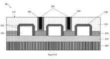
- Figure 6d shows a semiconductor device (501) obtained after contact fill metal (265) deposition and subsequently, a planarization step has been performed on this semiconductor structure (500).
- This contact metal (265) may be tungsten, copper, aluminum, cobalt or another low resistive metal that can be applied in a similar way.
- This planarization step is a chemical mechanical planarization (CMP) step.
- CMP chemical mechanical planarization
- This CMP step is performed until an end point is reached, whereby this Si or Ge comprising alloy (260) has been removed to, thereby, expose a top surface (225) of this insulating layer (220).
- This Ge comprising alloy is a mono-nickel-germanide (NiGe).
- This Si comprising alloy is a mono-nickel-silicide (NiSi).
- An electrical contact is thus, formed on an area (240) of this semiconductor structure (500). At the bottom of this through-hole (150) this electrical contact has an upper interface with this contact metal (265) and a lower interface with this vertical semiconductor body (175) on this area (240). This lower interface is a planar interface. The thickness variation of this electrical contact between this upper interface and this lower interface is less than ⁇ 1 nm.
- this electrical contact still has a planar interface with this sloped area.
- the thickness variation of this electrical contact between this upper interface and this lower interface on this sloped area is less than 1 nm.
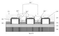
- Figure 7a and 7b show front view of the semiconductor structure (500) represented in Fig 5 according to an alternative embodiment of the method represented in the flowchart of Fig. 2 .
- the lithography and etch process used within the step (120) of defining an area on the semiconductor structure results in obtaining (through-holes) contact holes (150") having diameter (y) that is larger than the summation of spacer-to-spacer distance (x) between two neighboring gate stacks (290) and the total spacer thickness (2t) on both sides of this area (240").
- the diameter of the contact hole (150") is larger than the summation of the spacer-to-spacer distance (x) between two neighboring gate stacks (290) and the total spacer thickness (2 t ) on both sides of this area (240"), the diameter (y), in this case, cannot be that large such that contact holes (150") on either side of a gate stack (290) are merged.
- this contact hole (150") opens at its bottom to this area (240"), where this area exposes the complete contact region present between two neighboring gate stacks (290) having a spacer-to-spacer (x) separation distance.
- This contact region is, then, the complete top surface of the source region (280) and/or drain region (270) present on the top part of this vertical semiconductor body (175).
- This vertical semiconductor body is a fin structure and this area (240") is a contact area.
- This area (240") is bounded by sidewalls (155"). These sidewalls expose the insulating spacers (190). These exposed insulating spacers (190) are those that are present and face each other on opposite sides of two neighboring gate stacks (290). These sidewalls (155") of the contact hole (150") further expose this insulating layer (220).
- Ni (250) is provided conformally in the first tool covering the top surface (225) of this insulating layer (220), sidewalls (155") of this through-hole and this contact area (240")
- this metal (250), which is Ni may also be done in a selective way to result in Ni being present only on this area (240").
- Ni (250) is converted into a Si comprising or a Ge comprising alloy (260).
- This Ge comprising alloy is a mono-nickel-germanide (NiGe).
- This Si comprising alloy is a mono-nickel-silicide (NiSi).
- Fig. 7b shows a semiconductor device (502) obtained after contact fill metal (265) deposition and subsequently, a planarization step has been performed on this semiconductor structure (500) presented in Fig. 7a .
- An electrical contact is formed on an area (240") of this semiconductor structure (500). At the bottom of this through-hole (150") this electrical contact has an upper interface with this contact metal (265) and a lower interface with this vertical semiconductor body (175) on this area (240"). This lower interface is a planar interface. The thickness variation of this electrical contact between this upper interface and this lower interface is less than ⁇ 1 nm.
- the lithography and etch process used within the step (120) of defining an area on the semiconductor structure may result in obtaining (through-holes) contact holes having diameter (y) that is equal to the spacer-to-spacer distance (x) between two neighboring gate stacks.
- the lithography and etch process used within the step (120) of defining an area on the semiconductor structure may result in obtaining contact holes having diameter (y) that is equal to the summation of spacer-to-spacer distance (x) between two neighboring gate stacks and the total spacer thickness (2t) on both sides of this horizontal portion.
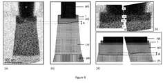
- FIG. 8a and Figure 8c show Transmission Electron Microscopy (TEM) images of a mono-nickel-germanide (NiGe) electrical contact produced by the state-of-the-art salmanide process.
- Figure 8b and Figure 8d are sketches of the TEM image presented in Fig. 8a and Fig. 8b , respectively.
- This NiGe electrical contact (260) is formed on a fin structure (175) made of Ge on Si substrate (180).
- a contact metal (265) which is tungsten (W), is deposited on this NiGe electrical contact (260). It is noted that due to the non-uniform reaction between the deposited nickel and germanium, the interface between NiGe and Ge is not planar.
- Ni has reacted more with Ge on the left side of the fin structure (175) compared to the right side, thereby leading to the formation of a non-planar interface between NiGe and Ge. This has led to a thickness variation of (indicated by " ⁇ " in Fig. 8b and Fig. 8d ) in the range of 10-15 nm of this NiGe/Ge interface between the left and the right side of the fin structure (175).
- a TiN layer (1) may be present between NiGe electrical contact (260) and W contact metal (265).
- the method described may be particularly suited for producing NiGe or NiSi electrical contacts to be used in an integrated circuit comprising multiple n-MOS and p-MOS transistors.
- the method described simplifies the electrical contact formation process since NiGe or NiSi electrical contacts can be formed simultaneously on n-MOS and p-MOS transistors thanks to the advantage that NiGe or NiSi formation, by the method described, is independent of the material onto which Ni is provided.
- this p-MOS and this n-MOS transistor or plurality of n-MOS and p-MOS transistors is/are desired to have different electrical contacts, for example NiGe on p-MOS transistor and NiSi on n-MOS transistor or an opposite combination
- a protective layer is deposited on this semiconductor structure.
- This protective layer may be SiO2, SiN, amorphous carbon or other hard mask.
- This protective layer is patterned and etched, thereby, leaving this protective layer (only) on a second transistor area and exposing a first transistor area.
- This first transistor area is a p-MOS transistor area.
- This second transistor area is a n-MOS transistor area.
- this semiconductor structure Subjecting this semiconductor structure to a Ge comprising precursor gas at a temperature in the range of 215 °C to 250 °C forms NiGe electrical contact on this first transistor area. Thereafter, this protective layer is removed from this second transistor area. Then, this semiconductor structure is subjected to a Si comprising precursor gas at a temperature in the range of 225 °C to 350 °C, to thereby form NiSi electrical contact on this second transistor area.
- this first transistor area having NiGe electrical contact may be coated with this protective layer.
- Coating with this protective layer comprises depositing this protective layer, patterning and etching to thereby leave this protective layer on this first transistor area having NiGe electrical contact.
- This semiconductor structure is then subjected to this Si comprising precursor gas. This forms NiSi electrical contact on this second transistor area.
Landscapes
- Engineering & Computer Science (AREA)
- Physics & Mathematics (AREA)
- Computer Hardware Design (AREA)
- Condensed Matter Physics & Semiconductors (AREA)
- General Physics & Mathematics (AREA)
- Microelectronics & Electronic Packaging (AREA)
- Power Engineering (AREA)
- Manufacturing & Machinery (AREA)
- Electrodes Of Semiconductors (AREA)
- Insulated Gate Type Field-Effect Transistor (AREA)
- Plasma & Fusion (AREA)
- Chemical & Material Sciences (AREA)
- Materials Engineering (AREA)
Priority Applications (2)
| Application Number | Priority Date | Filing Date | Title |
|---|---|---|---|
| EP14196804.0A EP3032575B1 (de) | 2014-12-08 | 2014-12-08 | Verfahren zur Herstellung eines elektrischen Kontaktes |
| US14/957,989 US9633853B2 (en) | 2014-12-08 | 2015-12-03 | Method for forming an electrical contact |
Applications Claiming Priority (1)
| Application Number | Priority Date | Filing Date | Title |
|---|---|---|---|
| EP14196804.0A EP3032575B1 (de) | 2014-12-08 | 2014-12-08 | Verfahren zur Herstellung eines elektrischen Kontaktes |
Publications (2)
| Publication Number | Publication Date |
|---|---|
| EP3032575A1 true EP3032575A1 (de) | 2016-06-15 |
| EP3032575B1 EP3032575B1 (de) | 2020-10-21 |
Family
ID=52011090
Family Applications (1)
| Application Number | Title | Priority Date | Filing Date |
|---|---|---|---|
| EP14196804.0A Active EP3032575B1 (de) | 2014-12-08 | 2014-12-08 | Verfahren zur Herstellung eines elektrischen Kontaktes |
Country Status (2)
| Country | Link |
|---|---|
| US (1) | US9633853B2 (de) |
| EP (1) | EP3032575B1 (de) |
Families Citing this family (8)
| Publication number | Priority date | Publication date | Assignee | Title |
|---|---|---|---|---|
| US10032912B2 (en) | 2014-12-31 | 2018-07-24 | Stmicroelectronics, Inc. | Semiconductor integrated structure having an epitaxial SiGe layer extending from silicon-containing regions formed between segments of oxide regions |
| US9548361B1 (en) | 2015-06-30 | 2017-01-17 | Stmicroelectronics, Inc. | Method of using a sacrificial gate structure to make a metal gate FinFET transistor |
| US9679899B2 (en) | 2015-08-24 | 2017-06-13 | Stmicroelectronics, Inc. | Co-integration of tensile silicon and compressive silicon germanium |
| US10002932B2 (en) * | 2016-11-07 | 2018-06-19 | Globalfoundries Inc. | Self-aligned contact protection using reinforced gate cap and spacer portions |
| CN110729387B (zh) * | 2019-10-24 | 2020-10-23 | 厦门乾照光电股份有限公司 | 发光二极管芯片及发光二极管芯片的制造方法 |
| US12087628B2 (en) * | 2021-10-25 | 2024-09-10 | Sandisk Technologies Llc | High aspect ratio via fill process employing selective metal deposition and structures formed by the same |
| US12525487B2 (en) | 2021-10-25 | 2026-01-13 | SanDisk Technologies, Inc. | High aspect ratio via fill process employing selective metal deposition and structures formed by the same |
| US12456688B2 (en) | 2021-10-25 | 2025-10-28 | SanDisk Technologies, Inc. | High aspect ratio via fill process employing selective metal deposition and structures formed by the same |
Citations (5)
| Publication number | Priority date | Publication date | Assignee | Title |
|---|---|---|---|---|
| US20070166974A1 (en) * | 2006-01-17 | 2007-07-19 | Fujitsu Limited | Fabrication process of a semiconductor device |
| US7517765B2 (en) | 2004-03-08 | 2009-04-14 | Interuniversitair Microelektronica Centrum (Imec) | Method for forming germanides and devices obtained thereof |
| US8580686B1 (en) | 2012-04-23 | 2013-11-12 | Globalfoundries Inc. | Silicidation and/or germanidation on SiGe or Ge by cosputtering Ni and Ge and using an intralayer for thermal stability |
| WO2013171235A1 (en) * | 2012-05-14 | 2013-11-21 | Imec | Method for manufacturing germanide interconnect structures and corresponding interconnect structures |
| US20140167264A1 (en) * | 2012-12-13 | 2014-06-19 | Globalfoundries Inc. | Integrated circuits and methods for fabricating integrated circuits with silicide contacts on non-planar structures |
Family Cites Families (12)
| Publication number | Priority date | Publication date | Assignee | Title |
|---|---|---|---|---|
| US6696368B2 (en) * | 2001-07-31 | 2004-02-24 | Micron Technology, Inc. | Titanium boronitride layer for high aspect ratio semiconductor devices |
| US7026243B2 (en) * | 2003-10-20 | 2006-04-11 | Micron Technology, Inc. | Methods of forming conductive material silicides by reaction of metal with silicon |
| FR2896339A1 (fr) * | 2006-01-18 | 2007-07-20 | St Microelectronics Crolles 2 | Procede de retrait selectif d'un metal non-siliciure |
| JP2007235093A (ja) * | 2006-01-31 | 2007-09-13 | Toshiba Corp | 半導体装置の製造方法 |
| KR101019700B1 (ko) * | 2008-04-28 | 2011-03-07 | 주식회사 하이닉스반도체 | 반도체 소자의 제조 방법 |
| US20090294871A1 (en) * | 2008-05-30 | 2009-12-03 | Advanced Micro Devices, Inc. | Semiconductor devices having rare earth metal silicide contact layers and methods for fabricating the same |
| JP5332947B2 (ja) * | 2009-06-25 | 2013-11-06 | 富士通セミコンダクター株式会社 | 半導体装置の製造方法 |
| FR2953989B1 (fr) | 2009-12-10 | 2012-05-18 | Commissariat Energie Atomique | Procede de formation de materiaux metalliques comportant des semi-conducteurs |
| JP2012064882A (ja) * | 2010-09-17 | 2012-03-29 | Toshiba Corp | 半導体装置およびその製造方法 |
| CN104011870B (zh) * | 2011-12-20 | 2017-03-01 | 英特尔公司 | 减小的接触电阻的自对准接触金属化 |
| US20140113425A1 (en) * | 2012-10-22 | 2014-04-24 | United Microelectronics Corp. | Method of fabricating semiconductor device |
| US8956942B2 (en) * | 2012-12-21 | 2015-02-17 | Stmicroelectronics, Inc. | Method of forming a fully substrate-isolated FinFET transistor |
-
2014
- 2014-12-08 EP EP14196804.0A patent/EP3032575B1/de active Active
-
2015
- 2015-12-03 US US14/957,989 patent/US9633853B2/en active Active
Patent Citations (5)
| Publication number | Priority date | Publication date | Assignee | Title |
|---|---|---|---|---|
| US7517765B2 (en) | 2004-03-08 | 2009-04-14 | Interuniversitair Microelektronica Centrum (Imec) | Method for forming germanides and devices obtained thereof |
| US20070166974A1 (en) * | 2006-01-17 | 2007-07-19 | Fujitsu Limited | Fabrication process of a semiconductor device |
| US8580686B1 (en) | 2012-04-23 | 2013-11-12 | Globalfoundries Inc. | Silicidation and/or germanidation on SiGe or Ge by cosputtering Ni and Ge and using an intralayer for thermal stability |
| WO2013171235A1 (en) * | 2012-05-14 | 2013-11-21 | Imec | Method for manufacturing germanide interconnect structures and corresponding interconnect structures |
| US20140167264A1 (en) * | 2012-12-13 | 2014-06-19 | Globalfoundries Inc. | Integrated circuits and methods for fabricating integrated circuits with silicide contacts on non-planar structures |
Non-Patent Citations (2)
| Title |
|---|
| BRUNCO, ELECTROCHEMICAL AND SOLID STATE LETTERS, vol. 11, no. 2, 2008 |
| PETER ET AL.: "Growth Evolution and Characterization of Ultra-Thin CoGe2 Films Synthesized via a Catalytic Solid-Vapour Reaction Technique", JOURNAL OF MATERIALS CHEMISTRY C, vol. 2, no. 10, 14 March 2014 (2014-03-14), pages 1904 - 1912, XP002740046, ISSN: 2050-7526, DOI: 10.1039/C3TC32135E * |
Also Published As
| Publication number | Publication date |
|---|---|
| EP3032575B1 (de) | 2020-10-21 |
| US20160163648A1 (en) | 2016-06-09 |
| US9633853B2 (en) | 2017-04-25 |
Similar Documents
| Publication | Publication Date | Title |
|---|---|---|
| US9633853B2 (en) | Method for forming an electrical contact | |
| US11133416B2 (en) | Methods of forming semiconductor devices having plural epitaxial layers | |
| TWI588907B (zh) | 包括鰭結構之半導體裝置及其製造方法 | |
| US12490508B2 (en) | Semiconductor device and method | |
| TW202029417A (zh) | 半導體裝置及其形成方法 | |
| CN107665864A (zh) | 具有气隙间隔件的finfet及其形成方法 | |
| US20220336202A1 (en) | Forming Low-Stress Silicon Nitride Layer Through Hydrogen Treatment | |
| US12009200B2 (en) | Treatment for adhesion improvement | |
| TW202008428A (zh) | 半導體元件 | |
| US20180145131A1 (en) | Semiconductor Device and Method | |
| CN108735604B (zh) | 晶体管的形成方法 | |
| TWI770748B (zh) | 半導體裝置及其製造方法 | |
| CN112951921A (zh) | 半导体器件及其制造方法 | |
| TW201731109A (zh) | 鰭片型場效應電晶體元件及其製造方法 | |
| US20250344449A1 (en) | Self-Aligned Contact Hard Mask Structure of Semiconductor Device and Method of Forming Same | |
| US11855095B2 (en) | Semiconductor device | |
| CN103515195A (zh) | 衬底电阻器及其制造方法 | |
| CN113130655B (zh) | 半导体器件及其制造方法 | |
| TWI747601B (zh) | 閘極電極的形成方法,電晶體及元件 | |
| CN115527935A (zh) | 半导体装置及其制造方法 | |
| TWI789761B (zh) | 半導體元件與其製造方法 | |
| US20250338599A1 (en) | Semiconductor gate structure and methods of forming the same | |
| WO2025207177A1 (en) | Method for semiconductor processing | |
| TW202145300A (zh) | 半導體裝置及其製造方法 | |
| CN110660726A (zh) | 半导体装置及其形成方法 |
Legal Events
| Date | Code | Title | Description |
|---|---|---|---|
| PUAI | Public reference made under article 153(3) epc to a published international application that has entered the european phase |
Free format text: ORIGINAL CODE: 0009012 |
|
| AK | Designated contracting states |
Kind code of ref document: A1 Designated state(s): AL AT BE BG CH CY CZ DE DK EE ES FI FR GB GR HR HU IE IS IT LI LT LU LV MC MK MT NL NO PL PT RO RS SE SI SK SM TR |
|
| AX | Request for extension of the european patent |
Extension state: BA ME |
|
| STAA | Information on the status of an ep patent application or granted ep patent |
Free format text: STATUS: REQUEST FOR EXAMINATION WAS MADE |
|
| 17P | Request for examination filed |
Effective date: 20161215 |
|
| RBV | Designated contracting states (corrected) |
Designated state(s): AL AT BE BG CH CY CZ DE DK EE ES FI FR GB GR HR HU IE IS IT LI LT LU LV MC MK MT NL NO PL PT RO RS SE SI SK SM TR |
|
| STAA | Information on the status of an ep patent application or granted ep patent |
Free format text: STATUS: EXAMINATION IS IN PROGRESS |
|
| 17Q | First examination report despatched |
Effective date: 20200313 |
|
| GRAP | Despatch of communication of intention to grant a patent |
Free format text: ORIGINAL CODE: EPIDOSNIGR1 |
|
| STAA | Information on the status of an ep patent application or granted ep patent |
Free format text: STATUS: GRANT OF PATENT IS INTENDED |
|
| RIC1 | Information provided on ipc code assigned before grant |
Ipc: H01L 29/417 20060101ALI20200709BHEP Ipc: H01L 21/285 20060101AFI20200709BHEP Ipc: H01L 21/768 20060101ALI20200709BHEP |
|
| INTG | Intention to grant announced |
Effective date: 20200804 |
|
| GRAS | Grant fee paid |
Free format text: ORIGINAL CODE: EPIDOSNIGR3 |
|
| GRAA | (expected) grant |
Free format text: ORIGINAL CODE: 0009210 |
|
| STAA | Information on the status of an ep patent application or granted ep patent |
Free format text: STATUS: THE PATENT HAS BEEN GRANTED |
|
| AK | Designated contracting states |
Kind code of ref document: B1 Designated state(s): AL AT BE BG CH CY CZ DE DK EE ES FI FR GB GR HR HU IE IS IT LI LT LU LV MC MK MT NL NO PL PT RO RS SE SI SK SM TR |
|
| REG | Reference to a national code |
Ref country code: GB Ref legal event code: FG4D |
|
| REG | Reference to a national code |
Ref country code: CH Ref legal event code: EP |
|
| REG | Reference to a national code |
Ref country code: IE Ref legal event code: FG4D |
|
| REG | Reference to a national code |
Ref country code: DE Ref legal event code: R096 Ref document number: 602014071399 Country of ref document: DE |
|
| REG | Reference to a national code |
Ref country code: AT Ref legal event code: REF Ref document number: 1326710 Country of ref document: AT Kind code of ref document: T Effective date: 20201115 |
|
| REG | Reference to a national code |
Ref country code: AT Ref legal event code: MK05 Ref document number: 1326710 Country of ref document: AT Kind code of ref document: T Effective date: 20201021 |
|
| REG | Reference to a national code |
Ref country code: NL Ref legal event code: MP Effective date: 20201021 |
|
| PG25 | Lapsed in a contracting state [announced via postgrant information from national office to epo] |
Ref country code: GR Free format text: LAPSE BECAUSE OF FAILURE TO SUBMIT A TRANSLATION OF THE DESCRIPTION OR TO PAY THE FEE WITHIN THE PRESCRIBED TIME-LIMIT Effective date: 20210122 Ref country code: NL Free format text: LAPSE BECAUSE OF FAILURE TO SUBMIT A TRANSLATION OF THE DESCRIPTION OR TO PAY THE FEE WITHIN THE PRESCRIBED TIME-LIMIT Effective date: 20201021 Ref country code: NO Free format text: LAPSE BECAUSE OF FAILURE TO SUBMIT A TRANSLATION OF THE DESCRIPTION OR TO PAY THE FEE WITHIN THE PRESCRIBED TIME-LIMIT Effective date: 20210121 Ref country code: PT Free format text: LAPSE BECAUSE OF FAILURE TO SUBMIT A TRANSLATION OF THE DESCRIPTION OR TO PAY THE FEE WITHIN THE PRESCRIBED TIME-LIMIT Effective date: 20210222 Ref country code: FI Free format text: LAPSE BECAUSE OF FAILURE TO SUBMIT A TRANSLATION OF THE DESCRIPTION OR TO PAY THE FEE WITHIN THE PRESCRIBED TIME-LIMIT Effective date: 20201021 Ref country code: RS Free format text: LAPSE BECAUSE OF FAILURE TO SUBMIT A TRANSLATION OF THE DESCRIPTION OR TO PAY THE FEE WITHIN THE PRESCRIBED TIME-LIMIT Effective date: 20201021 |
|
| REG | Reference to a national code |
Ref country code: LT Ref legal event code: MG4D |
|
| PG25 | Lapsed in a contracting state [announced via postgrant information from national office to epo] |
Ref country code: IS Free format text: LAPSE BECAUSE OF FAILURE TO SUBMIT A TRANSLATION OF THE DESCRIPTION OR TO PAY THE FEE WITHIN THE PRESCRIBED TIME-LIMIT Effective date: 20210221 Ref country code: PL Free format text: LAPSE BECAUSE OF FAILURE TO SUBMIT A TRANSLATION OF THE DESCRIPTION OR TO PAY THE FEE WITHIN THE PRESCRIBED TIME-LIMIT Effective date: 20201021 Ref country code: LV Free format text: LAPSE BECAUSE OF FAILURE TO SUBMIT A TRANSLATION OF THE DESCRIPTION OR TO PAY THE FEE WITHIN THE PRESCRIBED TIME-LIMIT Effective date: 20201021 Ref country code: SE Free format text: LAPSE BECAUSE OF FAILURE TO SUBMIT A TRANSLATION OF THE DESCRIPTION OR TO PAY THE FEE WITHIN THE PRESCRIBED TIME-LIMIT Effective date: 20201021 Ref country code: ES Free format text: LAPSE BECAUSE OF FAILURE TO SUBMIT A TRANSLATION OF THE DESCRIPTION OR TO PAY THE FEE WITHIN THE PRESCRIBED TIME-LIMIT Effective date: 20201021 Ref country code: AT Free format text: LAPSE BECAUSE OF FAILURE TO SUBMIT A TRANSLATION OF THE DESCRIPTION OR TO PAY THE FEE WITHIN THE PRESCRIBED TIME-LIMIT Effective date: 20201021 Ref country code: BG Free format text: LAPSE BECAUSE OF FAILURE TO SUBMIT A TRANSLATION OF THE DESCRIPTION OR TO PAY THE FEE WITHIN THE PRESCRIBED TIME-LIMIT Effective date: 20210121 |
|
| PG25 | Lapsed in a contracting state [announced via postgrant information from national office to epo] |
Ref country code: HR Free format text: LAPSE BECAUSE OF FAILURE TO SUBMIT A TRANSLATION OF THE DESCRIPTION OR TO PAY THE FEE WITHIN THE PRESCRIBED TIME-LIMIT Effective date: 20201021 |
|
| REG | Reference to a national code |
Ref country code: DE Ref legal event code: R097 Ref document number: 602014071399 Country of ref document: DE |
|
| PG25 | Lapsed in a contracting state [announced via postgrant information from national office to epo] |
Ref country code: RO Free format text: LAPSE BECAUSE OF FAILURE TO SUBMIT A TRANSLATION OF THE DESCRIPTION OR TO PAY THE FEE WITHIN THE PRESCRIBED TIME-LIMIT Effective date: 20201021 Ref country code: SK Free format text: LAPSE BECAUSE OF FAILURE TO SUBMIT A TRANSLATION OF THE DESCRIPTION OR TO PAY THE FEE WITHIN THE PRESCRIBED TIME-LIMIT Effective date: 20201021 Ref country code: LT Free format text: LAPSE BECAUSE OF FAILURE TO SUBMIT A TRANSLATION OF THE DESCRIPTION OR TO PAY THE FEE WITHIN THE PRESCRIBED TIME-LIMIT Effective date: 20201021 Ref country code: SM Free format text: LAPSE BECAUSE OF FAILURE TO SUBMIT A TRANSLATION OF THE DESCRIPTION OR TO PAY THE FEE WITHIN THE PRESCRIBED TIME-LIMIT Effective date: 20201021 Ref country code: EE Free format text: LAPSE BECAUSE OF FAILURE TO SUBMIT A TRANSLATION OF THE DESCRIPTION OR TO PAY THE FEE WITHIN THE PRESCRIBED TIME-LIMIT Effective date: 20201021 Ref country code: CZ Free format text: LAPSE BECAUSE OF FAILURE TO SUBMIT A TRANSLATION OF THE DESCRIPTION OR TO PAY THE FEE WITHIN THE PRESCRIBED TIME-LIMIT Effective date: 20201021 |
|
| REG | Reference to a national code |
Ref country code: CH Ref legal event code: PL |
|
| PLBE | No opposition filed within time limit |
Free format text: ORIGINAL CODE: 0009261 |
|
| STAA | Information on the status of an ep patent application or granted ep patent |
Free format text: STATUS: NO OPPOSITION FILED WITHIN TIME LIMIT |
|
| PG25 | Lapsed in a contracting state [announced via postgrant information from national office to epo] |
Ref country code: DK Free format text: LAPSE BECAUSE OF FAILURE TO SUBMIT A TRANSLATION OF THE DESCRIPTION OR TO PAY THE FEE WITHIN THE PRESCRIBED TIME-LIMIT Effective date: 20201021 Ref country code: MC Free format text: LAPSE BECAUSE OF FAILURE TO SUBMIT A TRANSLATION OF THE DESCRIPTION OR TO PAY THE FEE WITHIN THE PRESCRIBED TIME-LIMIT Effective date: 20201021 |
|
| REG | Reference to a national code |
Ref country code: BE Ref legal event code: MM Effective date: 20201231 |
|
| 26N | No opposition filed |
Effective date: 20210722 |
|
| GBPC | Gb: european patent ceased through non-payment of renewal fee |
Effective date: 20210121 |
|
| PG25 | Lapsed in a contracting state [announced via postgrant information from national office to epo] |
Ref country code: AL Free format text: LAPSE BECAUSE OF FAILURE TO SUBMIT A TRANSLATION OF THE DESCRIPTION OR TO PAY THE FEE WITHIN THE PRESCRIBED TIME-LIMIT Effective date: 20201021 Ref country code: FR Free format text: LAPSE BECAUSE OF NON-PAYMENT OF DUE FEES Effective date: 20201221 Ref country code: LU Free format text: LAPSE BECAUSE OF NON-PAYMENT OF DUE FEES Effective date: 20201208 Ref country code: IT Free format text: LAPSE BECAUSE OF FAILURE TO SUBMIT A TRANSLATION OF THE DESCRIPTION OR TO PAY THE FEE WITHIN THE PRESCRIBED TIME-LIMIT Effective date: 20201021 Ref country code: IE Free format text: LAPSE BECAUSE OF NON-PAYMENT OF DUE FEES Effective date: 20201208 |
|
| PG25 | Lapsed in a contracting state [announced via postgrant information from national office to epo] |
Ref country code: SI Free format text: LAPSE BECAUSE OF FAILURE TO SUBMIT A TRANSLATION OF THE DESCRIPTION OR TO PAY THE FEE WITHIN THE PRESCRIBED TIME-LIMIT Effective date: 20201021 Ref country code: CH Free format text: LAPSE BECAUSE OF NON-PAYMENT OF DUE FEES Effective date: 20201231 Ref country code: GB Free format text: LAPSE BECAUSE OF NON-PAYMENT OF DUE FEES Effective date: 20210121 Ref country code: LI Free format text: LAPSE BECAUSE OF NON-PAYMENT OF DUE FEES Effective date: 20201231 |
|
| PG25 | Lapsed in a contracting state [announced via postgrant information from national office to epo] |
Ref country code: IS Free format text: LAPSE BECAUSE OF FAILURE TO SUBMIT A TRANSLATION OF THE DESCRIPTION OR TO PAY THE FEE WITHIN THE PRESCRIBED TIME-LIMIT Effective date: 20210221 Ref country code: TR Free format text: LAPSE BECAUSE OF FAILURE TO SUBMIT A TRANSLATION OF THE DESCRIPTION OR TO PAY THE FEE WITHIN THE PRESCRIBED TIME-LIMIT Effective date: 20201021 Ref country code: MT Free format text: LAPSE BECAUSE OF FAILURE TO SUBMIT A TRANSLATION OF THE DESCRIPTION OR TO PAY THE FEE WITHIN THE PRESCRIBED TIME-LIMIT Effective date: 20201021 Ref country code: CY Free format text: LAPSE BECAUSE OF FAILURE TO SUBMIT A TRANSLATION OF THE DESCRIPTION OR TO PAY THE FEE WITHIN THE PRESCRIBED TIME-LIMIT Effective date: 20201021 |
|
| PG25 | Lapsed in a contracting state [announced via postgrant information from national office to epo] |
Ref country code: MK Free format text: LAPSE BECAUSE OF FAILURE TO SUBMIT A TRANSLATION OF THE DESCRIPTION OR TO PAY THE FEE WITHIN THE PRESCRIBED TIME-LIMIT Effective date: 20201021 |
|
| PG25 | Lapsed in a contracting state [announced via postgrant information from national office to epo] |
Ref country code: BE Free format text: LAPSE BECAUSE OF NON-PAYMENT OF DUE FEES Effective date: 20201231 |
|
| P01 | Opt-out of the competence of the unified patent court (upc) registered |
Effective date: 20230513 |
|
| REG | Reference to a national code |
Ref country code: DE Ref legal event code: R079 Ref document number: 602014071399 Country of ref document: DE Free format text: PREVIOUS MAIN CLASS: H01L0021285000 Ipc: H10D0064010000 |
|
| PGFP | Annual fee paid to national office [announced via postgrant information from national office to epo] |
Ref country code: DE Payment date: 20251126 Year of fee payment: 12 |