EP3031789A1 - Circuit substrate and semiconductor device - Google Patents
Circuit substrate and semiconductor device Download PDFInfo
- Publication number
- EP3031789A1 EP3031789A1 EP14835334.5A EP14835334A EP3031789A1 EP 3031789 A1 EP3031789 A1 EP 3031789A1 EP 14835334 A EP14835334 A EP 14835334A EP 3031789 A1 EP3031789 A1 EP 3031789A1
- Authority
- EP
- European Patent Office
- Prior art keywords
- circuit board
- copper circuit
- less
- copper
- diffusion region
- Prior art date
- Legal status (The legal status is an assumption and is not a legal conclusion. Google has not performed a legal analysis and makes no representation as to the accuracy of the status listed.)
- Granted
Links
Images


Classifications
-
- B—PERFORMING OPERATIONS; TRANSPORTING
- B23—MACHINE TOOLS; METAL-WORKING NOT OTHERWISE PROVIDED FOR
- B23K—SOLDERING OR UNSOLDERING; WELDING; CLADDING OR PLATING BY SOLDERING OR WELDING; CUTTING BY APPLYING HEAT LOCALLY, e.g. FLAME CUTTING; WORKING BY LASER BEAM
- B23K1/00—Soldering, e.g. brazing, or unsoldering
- B23K1/19—Soldering, e.g. brazing, or unsoldering taking account of the properties of the materials to be soldered
-
- B—PERFORMING OPERATIONS; TRANSPORTING
- B23—MACHINE TOOLS; METAL-WORKING NOT OTHERWISE PROVIDED FOR
- B23K—SOLDERING OR UNSOLDERING; WELDING; CLADDING OR PLATING BY SOLDERING OR WELDING; CUTTING BY APPLYING HEAT LOCALLY, e.g. FLAME CUTTING; WORKING BY LASER BEAM
- B23K1/00—Soldering, e.g. brazing, or unsoldering
- B23K1/0008—Soldering, e.g. brazing, or unsoldering specially adapted for particular articles or work
- B23K1/0016—Soldering of electronic components
-
- B—PERFORMING OPERATIONS; TRANSPORTING
- B23—MACHINE TOOLS; METAL-WORKING NOT OTHERWISE PROVIDED FOR
- B23K—SOLDERING OR UNSOLDERING; WELDING; CLADDING OR PLATING BY SOLDERING OR WELDING; CUTTING BY APPLYING HEAT LOCALLY, e.g. FLAME CUTTING; WORKING BY LASER BEAM
- B23K20/00—Non-electric welding by applying impact or other pressure, with or without the application of heat, e.g. cladding or plating
- B23K20/02—Non-electric welding by applying impact or other pressure, with or without the application of heat, e.g. cladding or plating by means of a press ; Diffusion bonding
- B23K20/023—Thermo-compression bonding
- B23K20/026—Thermo-compression bonding with diffusion of soldering material
-
- B—PERFORMING OPERATIONS; TRANSPORTING
- B23—MACHINE TOOLS; METAL-WORKING NOT OTHERWISE PROVIDED FOR
- B23K—SOLDERING OR UNSOLDERING; WELDING; CLADDING OR PLATING BY SOLDERING OR WELDING; CUTTING BY APPLYING HEAT LOCALLY, e.g. FLAME CUTTING; WORKING BY LASER BEAM
- B23K20/00—Non-electric welding by applying impact or other pressure, with or without the application of heat, e.g. cladding or plating
- B23K20/16—Non-electric welding by applying impact or other pressure, with or without the application of heat, e.g. cladding or plating with interposition of special material to facilitate connection of the parts, e.g. material for absorbing or producing gas
-
- B—PERFORMING OPERATIONS; TRANSPORTING
- B23—MACHINE TOOLS; METAL-WORKING NOT OTHERWISE PROVIDED FOR
- B23K—SOLDERING OR UNSOLDERING; WELDING; CLADDING OR PLATING BY SOLDERING OR WELDING; CUTTING BY APPLYING HEAT LOCALLY, e.g. FLAME CUTTING; WORKING BY LASER BEAM
- B23K20/00—Non-electric welding by applying impact or other pressure, with or without the application of heat, e.g. cladding or plating
- B23K20/22—Non-electric welding by applying impact or other pressure, with or without the application of heat, e.g. cladding or plating taking account of the properties of the materials to be welded
- B23K20/233—Non-electric welding by applying impact or other pressure, with or without the application of heat, e.g. cladding or plating taking account of the properties of the materials to be welded without ferrous layer
-
- C—CHEMISTRY; METALLURGY
- C04—CEMENTS; CONCRETE; ARTIFICIAL STONE; CERAMICS; REFRACTORIES
- C04B—LIME, MAGNESIA; SLAG; CEMENTS; COMPOSITIONS THEREOF, e.g. MORTARS, CONCRETE OR LIKE BUILDING MATERIALS; ARTIFICIAL STONE; CERAMICS; REFRACTORIES; TREATMENT OF NATURAL STONE
- C04B37/00—Joining burned ceramic articles with other burned ceramic articles or other articles by heating
- C04B37/02—Joining burned ceramic articles with other burned ceramic articles or other articles by heating with metallic articles
- C04B37/023—Joining burned ceramic articles with other burned ceramic articles or other articles by heating with metallic articles characterised by the interlayer used
-
- C—CHEMISTRY; METALLURGY
- C04—CEMENTS; CONCRETE; ARTIFICIAL STONE; CERAMICS; REFRACTORIES
- C04B—LIME, MAGNESIA; SLAG; CEMENTS; COMPOSITIONS THEREOF, e.g. MORTARS, CONCRETE OR LIKE BUILDING MATERIALS; ARTIFICIAL STONE; CERAMICS; REFRACTORIES; TREATMENT OF NATURAL STONE
- C04B37/00—Joining burned ceramic articles with other burned ceramic articles or other articles by heating
- C04B37/02—Joining burned ceramic articles with other burned ceramic articles or other articles by heating with metallic articles
- C04B37/023—Joining burned ceramic articles with other burned ceramic articles or other articles by heating with metallic articles characterised by the interlayer used
- C04B37/026—Joining burned ceramic articles with other burned ceramic articles or other articles by heating with metallic articles characterised by the interlayer used consisting of metals or metal salts
-
- H—ELECTRICITY
- H05—ELECTRIC TECHNIQUES NOT OTHERWISE PROVIDED FOR
- H05K—PRINTED CIRCUITS; CASINGS OR CONSTRUCTIONAL DETAILS OF ELECTRIC APPARATUS; MANUFACTURE OF ASSEMBLAGES OF ELECTRICAL COMPONENTS
- H05K3/00—Apparatus or processes for manufacturing printed circuits
- H05K3/38—Improvement of the adhesion between the insulating substrate and the metal
-
- H—ELECTRICITY
- H10—SEMICONDUCTOR DEVICES; ELECTRIC SOLID-STATE DEVICES NOT OTHERWISE PROVIDED FOR
- H10W—GENERIC PACKAGES, INTERCONNECTIONS, CONNECTORS OR OTHER CONSTRUCTIONAL DETAILS OF DEVICES COVERED BY CLASS H10
- H10W40/00—Arrangements for thermal protection or thermal control
- H10W40/20—Arrangements for cooling
- H10W40/25—Arrangements for cooling characterised by their materials
- H10W40/255—Arrangements for cooling characterised by their materials having a laminate or multilayered structure, e.g. direct bond copper [DBC] ceramic substrates
-
- H—ELECTRICITY
- H10—SEMICONDUCTOR DEVICES; ELECTRIC SOLID-STATE DEVICES NOT OTHERWISE PROVIDED FOR
- H10W—GENERIC PACKAGES, INTERCONNECTIONS, CONNECTORS OR OTHER CONSTRUCTIONAL DETAILS OF DEVICES COVERED BY CLASS H10
- H10W70/00—Package substrates; Interposers; Redistribution layers [RDL]
- H10W70/60—Insulating or insulated package substrates; Interposers; Redistribution layers
- H10W70/67—Insulating or insulated package substrates; Interposers; Redistribution layers characterised by their insulating layers or insulating parts
- H10W70/69—Insulating materials thereof
- H10W70/692—Ceramics or glasses
-
- B—PERFORMING OPERATIONS; TRANSPORTING
- B23—MACHINE TOOLS; METAL-WORKING NOT OTHERWISE PROVIDED FOR
- B23K—SOLDERING OR UNSOLDERING; WELDING; CLADDING OR PLATING BY SOLDERING OR WELDING; CUTTING BY APPLYING HEAT LOCALLY, e.g. FLAME CUTTING; WORKING BY LASER BEAM
- B23K2101/00—Articles made by soldering, welding or cutting
- B23K2101/36—Electric or electronic devices
- B23K2101/42—Printed circuits
-
- B—PERFORMING OPERATIONS; TRANSPORTING
- B23—MACHINE TOOLS; METAL-WORKING NOT OTHERWISE PROVIDED FOR
- B23K—SOLDERING OR UNSOLDERING; WELDING; CLADDING OR PLATING BY SOLDERING OR WELDING; CUTTING BY APPLYING HEAT LOCALLY, e.g. FLAME CUTTING; WORKING BY LASER BEAM
- B23K2103/00—Materials to be soldered, welded or cut
- B23K2103/08—Non-ferrous metals or alloys
- B23K2103/12—Copper or alloys thereof
-
- B—PERFORMING OPERATIONS; TRANSPORTING
- B23—MACHINE TOOLS; METAL-WORKING NOT OTHERWISE PROVIDED FOR
- B23K—SOLDERING OR UNSOLDERING; WELDING; CLADDING OR PLATING BY SOLDERING OR WELDING; CUTTING BY APPLYING HEAT LOCALLY, e.g. FLAME CUTTING; WORKING BY LASER BEAM
- B23K2103/00—Materials to be soldered, welded or cut
- B23K2103/18—Dissimilar materials
-
- B—PERFORMING OPERATIONS; TRANSPORTING
- B23—MACHINE TOOLS; METAL-WORKING NOT OTHERWISE PROVIDED FOR
- B23K—SOLDERING OR UNSOLDERING; WELDING; CLADDING OR PLATING BY SOLDERING OR WELDING; CUTTING BY APPLYING HEAT LOCALLY, e.g. FLAME CUTTING; WORKING BY LASER BEAM
- B23K2103/00—Materials to be soldered, welded or cut
- B23K2103/50—Inorganic materials other than metals or composite materials
- B23K2103/52—Ceramics
-
- C—CHEMISTRY; METALLURGY
- C04—CEMENTS; CONCRETE; ARTIFICIAL STONE; CERAMICS; REFRACTORIES
- C04B—LIME, MAGNESIA; SLAG; CEMENTS; COMPOSITIONS THEREOF, e.g. MORTARS, CONCRETE OR LIKE BUILDING MATERIALS; ARTIFICIAL STONE; CERAMICS; REFRACTORIES; TREATMENT OF NATURAL STONE
- C04B2237/00—Aspects relating to ceramic laminates or to joining of ceramic articles with other articles by heating
- C04B2237/02—Aspects relating to interlayers, e.g. used to join ceramic articles with other articles by heating
- C04B2237/12—Metallic interlayers
-
- C—CHEMISTRY; METALLURGY
- C04—CEMENTS; CONCRETE; ARTIFICIAL STONE; CERAMICS; REFRACTORIES
- C04B—LIME, MAGNESIA; SLAG; CEMENTS; COMPOSITIONS THEREOF, e.g. MORTARS, CONCRETE OR LIKE BUILDING MATERIALS; ARTIFICIAL STONE; CERAMICS; REFRACTORIES; TREATMENT OF NATURAL STONE
- C04B2237/00—Aspects relating to ceramic laminates or to joining of ceramic articles with other articles by heating
- C04B2237/02—Aspects relating to interlayers, e.g. used to join ceramic articles with other articles by heating
- C04B2237/12—Metallic interlayers
- C04B2237/122—Metallic interlayers based on refractory metals
-
- C—CHEMISTRY; METALLURGY
- C04—CEMENTS; CONCRETE; ARTIFICIAL STONE; CERAMICS; REFRACTORIES
- C04B—LIME, MAGNESIA; SLAG; CEMENTS; COMPOSITIONS THEREOF, e.g. MORTARS, CONCRETE OR LIKE BUILDING MATERIALS; ARTIFICIAL STONE; CERAMICS; REFRACTORIES; TREATMENT OF NATURAL STONE
- C04B2237/00—Aspects relating to ceramic laminates or to joining of ceramic articles with other articles by heating
- C04B2237/02—Aspects relating to interlayers, e.g. used to join ceramic articles with other articles by heating
- C04B2237/12—Metallic interlayers
- C04B2237/124—Metallic interlayers based on copper
-
- C—CHEMISTRY; METALLURGY
- C04—CEMENTS; CONCRETE; ARTIFICIAL STONE; CERAMICS; REFRACTORIES
- C04B—LIME, MAGNESIA; SLAG; CEMENTS; COMPOSITIONS THEREOF, e.g. MORTARS, CONCRETE OR LIKE BUILDING MATERIALS; ARTIFICIAL STONE; CERAMICS; REFRACTORIES; TREATMENT OF NATURAL STONE
- C04B2237/00—Aspects relating to ceramic laminates or to joining of ceramic articles with other articles by heating
- C04B2237/02—Aspects relating to interlayers, e.g. used to join ceramic articles with other articles by heating
- C04B2237/12—Metallic interlayers
- C04B2237/125—Metallic interlayers based on noble metals, e.g. silver
-
- C—CHEMISTRY; METALLURGY
- C04—CEMENTS; CONCRETE; ARTIFICIAL STONE; CERAMICS; REFRACTORIES
- C04B—LIME, MAGNESIA; SLAG; CEMENTS; COMPOSITIONS THEREOF, e.g. MORTARS, CONCRETE OR LIKE BUILDING MATERIALS; ARTIFICIAL STONE; CERAMICS; REFRACTORIES; TREATMENT OF NATURAL STONE
- C04B2237/00—Aspects relating to ceramic laminates or to joining of ceramic articles with other articles by heating
- C04B2237/30—Composition of layers of ceramic laminates or of ceramic or metallic articles to be joined by heating, e.g. Si substrates
- C04B2237/32—Ceramic
- C04B2237/34—Oxidic
- C04B2237/343—Alumina or aluminates
-
- C—CHEMISTRY; METALLURGY
- C04—CEMENTS; CONCRETE; ARTIFICIAL STONE; CERAMICS; REFRACTORIES
- C04B—LIME, MAGNESIA; SLAG; CEMENTS; COMPOSITIONS THEREOF, e.g. MORTARS, CONCRETE OR LIKE BUILDING MATERIALS; ARTIFICIAL STONE; CERAMICS; REFRACTORIES; TREATMENT OF NATURAL STONE
- C04B2237/00—Aspects relating to ceramic laminates or to joining of ceramic articles with other articles by heating
- C04B2237/30—Composition of layers of ceramic laminates or of ceramic or metallic articles to be joined by heating, e.g. Si substrates
- C04B2237/32—Ceramic
- C04B2237/36—Non-oxidic
- C04B2237/366—Aluminium nitride
-
- C—CHEMISTRY; METALLURGY
- C04—CEMENTS; CONCRETE; ARTIFICIAL STONE; CERAMICS; REFRACTORIES
- C04B—LIME, MAGNESIA; SLAG; CEMENTS; COMPOSITIONS THEREOF, e.g. MORTARS, CONCRETE OR LIKE BUILDING MATERIALS; ARTIFICIAL STONE; CERAMICS; REFRACTORIES; TREATMENT OF NATURAL STONE
- C04B2237/00—Aspects relating to ceramic laminates or to joining of ceramic articles with other articles by heating
- C04B2237/30—Composition of layers of ceramic laminates or of ceramic or metallic articles to be joined by heating, e.g. Si substrates
- C04B2237/32—Ceramic
- C04B2237/36—Non-oxidic
- C04B2237/368—Silicon nitride
-
- C—CHEMISTRY; METALLURGY
- C04—CEMENTS; CONCRETE; ARTIFICIAL STONE; CERAMICS; REFRACTORIES
- C04B—LIME, MAGNESIA; SLAG; CEMENTS; COMPOSITIONS THEREOF, e.g. MORTARS, CONCRETE OR LIKE BUILDING MATERIALS; ARTIFICIAL STONE; CERAMICS; REFRACTORIES; TREATMENT OF NATURAL STONE
- C04B2237/00—Aspects relating to ceramic laminates or to joining of ceramic articles with other articles by heating
- C04B2237/30—Composition of layers of ceramic laminates or of ceramic or metallic articles to be joined by heating, e.g. Si substrates
- C04B2237/40—Metallic
- C04B2237/407—Copper
-
- C—CHEMISTRY; METALLURGY
- C04—CEMENTS; CONCRETE; ARTIFICIAL STONE; CERAMICS; REFRACTORIES
- C04B—LIME, MAGNESIA; SLAG; CEMENTS; COMPOSITIONS THEREOF, e.g. MORTARS, CONCRETE OR LIKE BUILDING MATERIALS; ARTIFICIAL STONE; CERAMICS; REFRACTORIES; TREATMENT OF NATURAL STONE
- C04B2237/00—Aspects relating to ceramic laminates or to joining of ceramic articles with other articles by heating
- C04B2237/50—Processing aspects relating to ceramic laminates or to the joining of ceramic articles with other articles by heating
- C04B2237/59—Aspects relating to the structure of the interlayer
-
- C—CHEMISTRY; METALLURGY
- C04—CEMENTS; CONCRETE; ARTIFICIAL STONE; CERAMICS; REFRACTORIES
- C04B—LIME, MAGNESIA; SLAG; CEMENTS; COMPOSITIONS THEREOF, e.g. MORTARS, CONCRETE OR LIKE BUILDING MATERIALS; ARTIFICIAL STONE; CERAMICS; REFRACTORIES; TREATMENT OF NATURAL STONE
- C04B2237/00—Aspects relating to ceramic laminates or to joining of ceramic articles with other articles by heating
- C04B2237/50—Processing aspects relating to ceramic laminates or to the joining of ceramic articles with other articles by heating
- C04B2237/60—Forming at the joining interface or in the joining layer specific reaction phases or zones, e.g. diffusion of reactive species from the interlayer to the substrate or from a substrate to the joining interface, carbide forming at the joining interface
-
- C—CHEMISTRY; METALLURGY
- C04—CEMENTS; CONCRETE; ARTIFICIAL STONE; CERAMICS; REFRACTORIES
- C04B—LIME, MAGNESIA; SLAG; CEMENTS; COMPOSITIONS THEREOF, e.g. MORTARS, CONCRETE OR LIKE BUILDING MATERIALS; ARTIFICIAL STONE; CERAMICS; REFRACTORIES; TREATMENT OF NATURAL STONE
- C04B2237/00—Aspects relating to ceramic laminates or to joining of ceramic articles with other articles by heating
- C04B2237/50—Processing aspects relating to ceramic laminates or to the joining of ceramic articles with other articles by heating
- C04B2237/88—Joining of two substrates, where a substantial part of the joining material is present outside of the joint, leading to an outside joining of the joint
-
- H—ELECTRICITY
- H05—ELECTRIC TECHNIQUES NOT OTHERWISE PROVIDED FOR
- H05K—PRINTED CIRCUITS; CASINGS OR CONSTRUCTIONAL DETAILS OF ELECTRIC APPARATUS; MANUFACTURE OF ASSEMBLAGES OF ELECTRICAL COMPONENTS
- H05K1/00—Printed circuits
- H05K1/02—Details
- H05K1/03—Use of materials for the substrate
- H05K1/0306—Inorganic insulating substrates, e.g. ceramic, glass
-
- H—ELECTRICITY
- H05—ELECTRIC TECHNIQUES NOT OTHERWISE PROVIDED FOR
- H05K—PRINTED CIRCUITS; CASINGS OR CONSTRUCTIONAL DETAILS OF ELECTRIC APPARATUS; MANUFACTURE OF ASSEMBLAGES OF ELECTRICAL COMPONENTS
- H05K2203/00—Indexing scheme relating to apparatus or processes for manufacturing printed circuits covered by H05K3/00
- H05K2203/11—Treatments characterised by their effect, e.g. heating, cooling, roughening
- H05K2203/1105—Heating or thermal processing not related to soldering, firing, curing or laminating, e.g. for shaping the substrate or during finish plating
Definitions
- the embodiment generally relates to a circuit substrate and a semiconductor device.
- a power module for controlling a large current/high voltage is used in an electric vehicle, an electric railcar, etc, in view of a high performance of an industrial equipment, a global environmental problem, and so on.
- a semiconductor element such as a SiC element having a high output is being developed as a semiconductor element.
- a circuit substrate having an excellent durability is demanded as a circuit substrate to mount a semiconductor element.
- the circuit substrate there can be cited a ceramic substrate, an insulating circuit substrate having a metal circuit board, and so on.
- a reliability of the circuit substrate is evaluated by a TCT (Temperature Cycle Test).
- the TCT is an inspection method for investigating presence/absence of peeling of a metal circuit board, presence/absence of a crack of a ceramic substrate, or the like in a circuit substrate, after a processing of keeping a low temperature ⁇ keeping a room temperature ⁇ keeping a high temperature is repeated a certain number of cycles.
- the reliability evaluated by the TCT is also referred to as a TCT reliability.
- circuit substrate having a high TCT reliability there is known a circuit substrate which has a copper circuit board having an end surface of a broad base shape as a broad base of Mt. Fuji.
- the copper circuit board having the end surface of the broad base shape is formed by processing an end surface to be gently inclined, for example.
- the copper circuit board having the end surface of the broad base shape its thickness is required to be 0.8 mm or less.
- the end surface of the broad base shape is formed by etching a copper circuit board, for example.
- a chemical solution such as ferric chloride and cupric chloride.
- etching of the copper circuit board is difficult if the thickness of the copper circuit board is larger than 0.8 mm, though an etching technique enabling etching of a thick copper circuit board is being developed.
- there are problems not only that a cost is high but also that waste water disposal affects an environment.
- the semiconductor element becomes to have a higher output, it is necessary to apply a large current or a high voltage to the semiconductor element. Thus, it is desired to heighten a cooling effect of a circuit substrate by thickening the copper circuit board.
- the thickness of the copper circuit board exceeds 0.7 mm, the TCT reliability is sometimes reduced due to a high thermal expansion coefficient of the copper circuit board.
- An embodiment provides a circuit substrate which has a high TCT reliability even when a copper circuit board is thickened and which has a high degree of freedom in circuit design.
- a circuit substrate includes: a ceramic substrate having a first surface and a second surface facing the first surface; a copper circuit board which is provided on at least either one of the first surface and the second surface of the ceramic substrate and which has a thickness T (mm) of 0.7 mm or more, an angle ⁇ of 85° or more to 95° or less of an interior angle in a cross section, and a semiconductor element mounting portion of 25 mm 2 or more provided in a surface; and a bonding layer bonding the ceramic substrate and the copper circuit board.
- the bonding layer has a protruding portion protruding outside the copper circuit board, provided in a manner to creep up along a side surface of the copper circuit board, and having a protruding amount W 1 of 0.1 mm or more to 1.0 mm or less and a creeping-up amount W2 of 0.05T (mm) or more to 0.6T (mm) or less.
- Fig. 1 is a diagram showing a configuration example of a circuit substrate.
- a circuit substrate 1 shown in Fig. 1 has a ceramic substrate 2, a copper circuit board 3, and a bonding layer 4.
- the ceramic substrate 2 has a first surface and a second surface facing the first surface, for example.
- the ceramic substrate 2 it is possible to use a silicon nitride substrate, an aluminum nitride substrate, an aluminum oxide substrate, or the like, for example.
- the silicon nitride substrate it is possible to use a silicon nitride substrate having a heat conductivity of 70 W/m.K or more and having a bending strength (three-point bending strength) by a three-point bending test of 600 MPa or more, for example.
- the silicon nitride substrate has a high strength even in a case of having a heat conductivity of 70 W/m.K or more to 110 W/m.K or less, for example.
- a thickness be 0.1 mm or more to 1.0 mm or less, preferably be 0.1 mm or more to 0.4 mm or less.
- the three-point bending strength of the silicon nitride substrate is more preferable to be 650 MPa or more.
- the aluminum nitride substrate it is possible to use an aluminum nitride substrate having a heat conductivity of 160 W/m.K or more and having a three-point bending strength of 300 MPa or more, for example.
- a strength of the aluminum nitride substrate is as low as 300 MPa or more to 550 MPa or less.
- a thickness of the aluminum nitride substrate is preferable to be 0.5 mm or more to 1.2 mm or less.
- the heat conductivity be 160 W/m.K or more, and further, be 200 W/m.K or more.
- the aluminum oxide substrate it is possible to use an aluminum oxide substrate having a heat conductivity of 20 W/m.K or more to 40 W/m.K or less and having a three-point bending strength of 400 MPa or more, for example.
- the aluminum oxide substrate is less expensive than the silicon nitride substrate and the aluminum nitride substrate.
- the copper circuit board 3 is provided on one side surface (first surface) of the ceramic substrate 2.
- the copper circuit board 3 is bonded to the first surface of the ceramic substrate 2 while sandwiching the bonding layer 4.
- the copper circuit board 3 has a semiconductor element mounting portion provided on a surface. On this occasion, the copper circuit board 3 is preferable to have an interior angle of an angle ⁇ (also referred to as a sectional angle ⁇ of an end portion) of 85° or more to 95° or less in a cross section.
- an angle ⁇ also referred to as a sectional angle ⁇ of an end portion
- the interior angle of the copper circuit board 3 is made to be almost right-angled in the cross section of the coper circuit board 3, it is possible to use the copper circuit board 3 end portion as the semiconductor element mounting portion. Further, it becomes easy to detect the copper circuit board 3 end portion by a position detector such as a CCD camera. In order to improve a detection accuracy of the copper circuit board 3 end portion, it is preferable to make the angle ⁇ be 89° or more to 91° or less, and further, be 90°.
- An area of the semiconductor element mounting portion is preferable to be 25 mm 2 or more. A degree of freedom in circuit design can be heightened by making the area of the semiconductor element mounting portion large. The area of the semiconductor element mounting portion is more preferable to be 1 cm 2 or more (100 mm 2 or more).
- the area of the semiconductor element mounting portion is a surface area of the copper circuit board 3 which is usable as a mounting region of a semiconductor element.
- the semiconductor element mounting portion is provided on an upper surface of the copper circuit board 3.
- a quadrangle shape such as a square shape and a rectangle shape, for example.
- a method of carrying out press forming for the copper circuit board 3 is effective.
- the shape of the semiconductor element mounting portion is preferable to be a simple shape such as a quadrangle shape.
- the surface shape of the semiconductor element mounting portion is the quadrangle shape, at least one edge may have a wave line shape or an S shape.
- the surface shape of the semiconductor element mounting portion may be a circular shape, an oval shape, a polygon shape, or the like.
- a thickness T of the copper circuit board 3 is preferable to be 0.7 mm or more.
- An upper limit of the thickness of the copper circuit board 3 is not limited in particular, but is preferable to be 7 mm or less, for example. When the thickness exceeds 7 mm, it becomes hard to adjust the angle ⁇ of the interior angle of the copper circuit board 3 to be 85° or more to 95° or less in the cross section.
- the thickness T of the copper circuit board 3 is more preferable to be 1 mm or more to 7 mm or less, and further, to be 2 mm or more to 5 mm or less.
- the bonding layer 4 bonds the ceramic substrate 2 and the copper circuit board 3.
- the bonding layer 4 is preferable to contain Ag, Cu, and Ti, for example.
- An Ag concentration of the bonding layer 4 is preferable to be 50 mass% or more to 80 mass% or less, a Cu concentration is preferable to be 20 mass% or more to 50 mass% or less, and a Ti concentration is preferable to be 1 mass% or more to 7 mass% or less.
- the bonding layer 4 is formed, for example, as a result that an active metal brazing material paste containing Ag, Cu, and Ti are applied and thereafter heated to be fixed to the ceramic substrate 2 and the copper circuit board 3.
- the bonding layer 4 may be a reaction layer of a metal component contained in the active metal brazing material and the copper circuit board 3, for example.
- a thickness of the bonding layer 4 is preferable to be 20 ⁇ m or more to 200 ⁇ m or less.
- the thickness of the bonding layer 4 is less than 20 ⁇ m, a not-bonded part of the ceramic substrate 2 and the copper circuit board 3 is liable to be formed. Further, when the thickness of the bonding layer 4 exceeds 200 ⁇ m, a characteristic such as a bonding strength is hard to be improved.
- a thickness of a portion sandwiched by the ceramic substrate 2 and the copper circuit board 3 of the bonding layer 4 may be regarded as the thickness of the bonding layer 4.
- a boning strength (peel strength) of the copper circuit board 3 to the ceramic substrate 2 is preferable to be 10 kN/m or more.
- the bonding layer 4 has a protruding portion which protrudes toward the outside of the copper circuit board 3.
- the protruding portion is provided in a manner to creep up along a side surface of the copper circuit board 3.
- a part of the copper circuit board 3 is embedded in the bonding layer 4 in a thickness direction.
- a width of the protruding portion is referred to as a protruding amount W1 of the bonding layer 4.
- a length (depth of a portion embedded in the bonding layer 4 of the copper circuit board 3) of a portion contacting a side surface of the copper circuit board by creeping-up of the bonding layer 4 is referred to as a creeping-up amount W2 of the bonding layer 4.
- Values of the protruding amount W1 and the creeping-up amount W2 can be controlled by a composition of the active metal grazing material paste or a heat treatment condition at a bonding time, for example.
- the protruding amount W1 is preferable to be 0.1 mm or more to 2 mm or less, for example.
- the protruding amount W1 is less than 0.1 mm, relaxation of stress is liable to be insufficient.
- the relaxation of stress is insufficient, the TCT reliability becomes liable to be reduced.
- the protruding width W1 exceeds 2 mm, a characteristic such as a bonding strength is hard to be improved. Further, a space where the copper circuit board 3 is disposed on the ceramic substrate 2 becomes smaller, a size of the circuit substrate 1 is liable to be large.
- the protruding amount W1 is more preferable to be 0.1 mm or more to 1.0 mm or less, and further, to be 0.2 mm or more to be 0.7 mm or less.
- the creeping-up amount W2 is preferable to be 0.05T (mm) or more to 0.6T (mm) or less in relation to the thickness T (mm) of the copper circuit board 3, for example.
- the creeping-up amount W2 is less than 0.05T (mm), that is, less than 10% of the thickness T of the copper circuit board 3, relaxation of stress is liable to be insufficient.
- the creeping-up amount W2 exceeds 0.6T (mm), a characteristic such as a bonding strength is hard to be improved. Further, the bonding layer 4 runs down and it becomes difficult to adjust the protruding amount W1 to be 2 mm or less.
- the creeping-up amount W2 is more preferable to be 0.1T (mm) or more to 0.4T (mm) or less.
- the protruding amount W1 and the creeping-up amount W2 are within the above-described range, stress is relaxed and the TCT reliability can be heightened even if a large-sized copper circuit board having a thickness T (mm) of 0.7 mm or more and a surface area of 25 mm 2 or more of a semiconductor element mounting portion is bonded to a ceramic substrate.
- the semiconductor element mounting portion can be provided in the end portion because of the copper circuit board having the interior angle of the angle ⁇ of 85° or more to 95° or less in the cross section, increase of the area of the circuit substrate is suppressed, so that the circuit substrate can be made small-sized.
- a semiconductor device using the circuit substrate according to the embodiment has a high cooling effect, and a semiconductor element of high output can be mounted thereon. Further, a degree of freedom in design becomes high, a product can be made small-sized, and the TCT reliability can be improved.
- the copper circuit board 3 may have a diffusion region in which at least a part of components of the bonding layer 4 is diffused.
- the diffusion region contains at least Ti, and contains Ag, Cu, and Ti, for example.
- a thickness of the diffusion region is preferable to be 0.01 mm (10 ⁇ m) or more.
- the bonding strength is improved, and it is possible to make the bonding strength (peel strength) of the copper circuit board 3 to the ceramic substrate 2 be 15 kN/m or more, for example.
- the thickness of the diffusion region is preferable to be 0.2 mm (200 ⁇ m) or less. When the thickness of the diffusion region exceeds 0.2 mm, a heating time period becomes long and too much stress is applied to the copper circuit board 3.
- the thickness of the diffusion region is more preferable to be 10 ⁇ m or more to 120 ⁇ m or less, and further, to be 20 ⁇ m or more to 100 ⁇ or less.
- the thickness of the bonding layer 4 be 30 ⁇ m or more to 100 ⁇ m or less.
- Fig. 2 is a diagram showing an example of the diffusion region.
- a circuit substrate 1 shown in Fig. 2 has a diffusion region 5, a diffusion region 6, and a diffusion region 7, in addition to a configuration shown in Fig. 1 .
- the diffusion region 5 is a width direction diffusion region formed along a bonding surface (side surface of a cooper circuit board 3) to a bonding layer 4 in a width direction of the copper circuit board 3.
- the diffusion region 6 is a thickness direction diffusion region formed along a bonding surface (bottom surface of the copper circuit board 3) to the bonding layer 4 in a thickness direction of the copper circuit board 3. Note that a thickness of the diffusion region 6 is a length in a width direction of the copper circuit board 3. Further, the diffusion region 5 to the diffusion region 7 may be regarded as one continuous diffusion region.
- the diffusion region 7 is provided in an end portion of the bonding surface to the bonding layer 4 in the width direction and the thickness direction of the copper circuit board 3. In other words, the diffusion region 7 is provided in an overlap portion of the diffusion region 5 and the diffusion region 6. A Ti concentration of the diffusion region 7 is higher than each Ti concentration of the diffusion region 5 and the diffusion region 6. Thus, the diffusion region 7 is also referred to as a Ti-rich region. By providing the diffusion region 7 being the Ti-rich region, it is possible to suppress heat expansion of the copper circuit board 3 end portion to which stress is liable to be applied.
- the Ti concentration of the diffusion region 7 is higher than an average value of the Ti concentrations of the diffusion regions by 30% or more of the average value.
- the average value of the Ti concentrations of the diffusion regions means an average value of values obtained by measuring respective Ti concentrations of the diffusion region 5 and the diffusion region 6.
- the Ti concentration of the diffusion region 7 is preferable to be higher than the average value of the Ti concentrations of the diffusion regions by 30% or more to 70% or less of the average value.
- a linear expansion coefficient of each element at a room temperature (25°C) is 8.4 ⁇ 10 -6 /K in a case of Ti, 16.6 ⁇ 10 -6 /K in a case of Cu, and 19.0 ⁇ 10 -6 /K in a case of Ag.
- a linear expansion coefficient (25°C) of a ceramic substrate 2 is 6.7 ⁇ 10 -6 /K or more to 7.4 ⁇ 10 -6 /K or less in a case of an aluminum oxide substrate, 4.5 ⁇ 10 -6 /K or more to 5.5 ⁇ 10 -6 /K or less in a case of an aluminum nitride substrate, and 2.5 ⁇ 10 -6 /K or more to 3.5 ⁇ 10 -6 /K or less in a case of a silicon nitride substrate.
- An upper limit of the area of the diffusion region 7 is not limited in particular, but is preferable to be 500000 ⁇ m 2 or less.
- Ranges of diffusion regions of Ag, Cu, and Ti in the diffusion region 5, the diffusion region 6, and the diffusion region 7 can be measured by an EPMA (Electron Probe Micro Analyzer), for example.
- EPMA Electro Probe Micro Analyzer
- color mapping is carried out in a range of a width of 500 ⁇ m or more in the width direction of the copper circuit board 3.
- color mapping is carried out in a range of a width of 500 ⁇ m or more in the thickness direction of the copper circuit board 3.
- color mapping is carried out in a range of 500 ⁇ m ⁇ 500 ⁇ m or more in the width direction and the thickness direction of the copper circuit board 3.
- ICP Inductively Coupled Plasma
- Sn and In are (is) diffused also to the diffusion region 5, the diffusion region 6, and the diffusion region 7. Therefore, similarly to in a case of Ag, Cu, Ti, by analyzing the cross section of the copper circuit board 3 by the EPMA, it is possible to analyze a diffusion state of Sn or In.
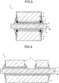
- Fig. 3 is a diagram showing an example of the circuit substrate which has copper circuit boards on both sides of a ceramic substrate.
- a circuit substrate 1 shown in Fig. 3 has a ceramic substrate 2, a copper circuit board 3 (front copper circuit board) and a copper circuit board 8 (rear copper circuit board).
- the circuit substrate 1 shown in Fig. 3 for components the same as those in the circuit substrates 1 shown in Fig. 1 and Fig. 2 , explanation of the circuit substrates 1 shown in Fig. 1 and Fig. 2 can be cited properly.
- the copper circuit board 8 is bonded to one surface (second surface) of the ceramic substrate 2 while sandwiching a bonding layer 4b.
- a similar material to that of the copper circuit board 3 can be used.
- the bonding layer 4b which has a similar function to that of a bonding layer 4, a similar material can be used.
- a protruding amount W1 and a creeping-up amount W2 of the bonding layer 4b may have values similar to those of the bonding layer 4.
- the protruding amount W1 of the bonding layer 4b is preferable to be 0.1 mm or more to 2 mm or less.
- the creeping-up amount W2 of the bonding layer 4b is preferable to be 0.05T (mm) or more to 0.6T (mm) or less.
- the copper circuit board 8 may have a diffusion region 5, a diffusion region 6, and a diffusion region 7.
- Fig. 4 is a diagram showing an example of a circuit substrate having a plurality of copper circuit boards on one side of a ceramic substrate.
- a circuit substrate 1 shown in Fig. 4 has a ceramic substrate 2, two copper circuit boards 3, and a copper circuit board 8.
- the circuit substrate 1 shown in Fig. 4 for components the same as those in the circuit substrates 1 shown in Fig. 1 to Fig. 3 , explanation of the circuit substrates 1 shown in Fig. 1 to Fig. 3 can be cited properly.
- Each of the two copper circuit boards 3 is bonded to the ceramic substrate 2 while sandwiching a bonding layer 4.
- a thickness T of each copper circuit board 3 is 0.7 mm or more, that a protruding amount W1 is 0.1 mm or more to 2 mm or less, and that a creeping-up amount W2 is 0.05T (mm) or more to 0.6T (mm) or less.
- Fig. 4 illustrates the example in which two copper circuit boards 3 are disposed, three or more copper circuit boards 3 may be disposed. Note that the diffusion region 5 to the diffusion region 7 shown in Fig. 2 and Fig. 3 may be formed in the copper circuit boards 3 and the copper circuit board 8 which are shown in Fig. 4 .
- a thickness of the copper circuit board 8 is preferable to be 0.7 mm or more, and further, to be 1 mm or more.
- a volume of the copper circuit board 8 may be the same as a volume of the copper circuit board 3.
- the copper circuit board 8 has a function to prevent warpage of the circuit substrate 1. By bonding the copper circuit board 8 with the volume almost equal to the volume of the copper circuit substrate 3, warpage can be prevented. Further, as shown in Fig. 4 , when the plurality of copper circuit boards 3 are disposed, it is preferable that a total volume of the circuit boards 3 and the volume of the copper circuit board 8 are made to be almost equal.
- a TCT reliability can be heightened. Further, since the copper circuit board of the thickness of 0.7 mm or more is bonded to the ceramic substrate, it is possible to apply a large current/high voltage. Further, the TCT reliability can be heightened even if a semiconductor element having a high operating temperature such as a SiC element is mounted on the circuit substrate.
- the reduction rate of the bonding strength (peel strength) be 10% or less even after 3000 cycles of TCTs, and further, 5000 cycles of TCTs.
- FIG. 5 is a diagram showing an example of the semiconductor device.
- a semiconductor device 10 shown in Fig. 5 has a ceramic substrate 2, a copper circuit board 3 provided on a first surface of the ceramic substrate 2, a bonding layer 4 bonding the first surface of the ceramic substrate and the copper circuit board 3, a copper circuit board 8 provided on a second surface of the ceramic substrate 2, a bonding layer 4b bonding the second surface of the ceramic substrate 2 and the copper circuit board 8, and a semiconductor element 9.
- a diffusion region 5 to a diffusion region 7 may be formed in each of the copper circuit board 3 and the copper circuit board 8.
- the diffusion regions 5 to the diffusion regions 7 shown in Fig. 2 and Fig. 3 may be formed in the copper circuit board 3 and the copper circuit board 8 which are shown in Fig. 5 .
- the semiconductor element 9 is bonded onto the copper circuit board 3 while sandwiching a bonding brazing material. Since the copper circuit board 3 has an interior angle of an angle ⁇ of 85° or more to 95° or less in a cross section, a semiconductor element mounting portion can be provided in a manner to include a position of 0.1 mm or more to 2 mm or less from a copper circuit board 3 end portion. In other words, it is possible to mount the semiconductor element 9 at the position of 0.1 mm or more to 2 mm or less from the copper circuit board 3 end portion. Further, it is also possible to mount the semiconductor element 9 at a position of 0.1 mm or more to 1.0 mm or less from the copper circuit board 3 end portion.
- the copper circuit board 3 Since the copper circuit board 3 has the interior angle of the angle ⁇ of 85° or more to 95° or less in the cross section, it is easy to detect a position of the semiconductor element mounting portion by a CCD (Charge Coupled Device) camera or the like. Therefore, it becomes easier to use the above-described circuit substrate as a circuit substrate used for a semiconductor device.
- CCD Charge Coupled Device
- the manufacturing method for the circuit substrate is not limited in particular as long as the above-described configuration of the circuit substrate can be satisfied, but as an efficient manufacturing method for a circuit substrate, a method below can be cited, for example.
- a ceramic substrate 2 is prepared.
- a silicon nitride substrate, an aluminum nitride substrate, an aluminum oxide substrate, or the like can be used as described above.
- a brazing material is preferable to be an active metal brazing material.
- an Ag concentration is in a range of 50 mass% or more to 80 mass% or less
- a Cu concentration is in a range of 20 mass% or more to 50 mass% or less
- a Ti concentration is in a range of 1 mass% or more to 7 mass% or less.
- the active metal brazing material it is possible to add either one or both of Sn and In at a ratio of 5 mass% or more to 25 mass% or less, other than Ag, Cu, and Ti.
- the active metal brazing material paste can be prepared. Note that an average grain diameter of each metal powder is preferable to be 1 ⁇ m or more to 7 ⁇ m or less.
- a thickness of a coating layer of the active metal brazing material paste is preferable to be 10 ⁇ m or more to 50 ⁇ m or less.
- the thickness of the coating layer is less than 10 ⁇ m, it becomes hard to form a diffusion region in a copper circuit board. Further, when the thickness of the coating layer exceeds 50 ⁇ m, a characteristic such as a bonding strength is hard to be improved, causing cost increase.
- the thickness of the coating layer is more preferable to be 20 ⁇ m or more to 40 ⁇ m or less.
- a copper circuit board is disposed on a part of the coating layer.
- the copper circuit board it is preferable to dispose the copper circuit board by applying stress.
- the applied brazing material paste slightly spreads.
- a protruding portion of the bonding layer can be formed.
- an active metal brazing material paste may be added. Also in a case where a rear copper circuit board is provided or a case where a plurality of front copper circuit boards are provided, it is preferable to carry out a processing similar to the above.
- the copper circuit board it is possible to use a copper circuit board having been processed to have a target size by a press work or a cutting process. By using the press work or the cutting process, it becomes easier to adjust an angle ⁇ of an interior angle to be 85° or more to 95° or less in a cross section.
- heat bonding is carried out.
- heating is carried out at 700°C or more to 900°C or less for 10 minutes or more to 150 minutes or less in a vacuum (1 ⁇ 10 -2 Pa or less) or in an inert atmosphere such as a nitrogen atmosphere. It is preferable to heat for 10 minutes or more in order to form a diffusion region. Further, it is preferable to heat for 30 minutes or more in order to form a Ti-rich region.
- a heat bonding step it is also effective to carry out the heat bonding step in a nitrogen atmosphere (10 Pa or more) until a temperature reaches less than 500°C and in a vacuum (1 ⁇ 10 -2 Pa or less) after the temperature reaches 500°C or more.
- a heat processing in the nitrogen atmosphere it is possible to accelerate generation of TiN (titanium nitride) in the bonding layer.
- a gas component generated by the active metal brazing material paste it is possible to make it easier to let out a gas component generated by the active metal brazing material paste. As a result, a peel strength of the copper circuit board to the ceramic substrate becomes high.
- the heat bonding step it is also effective to carry out heat bonding while switching heat bonding in the vacuum (1 ⁇ 10 -2 Pa or less) and heat bonding in the nitrogen atmosphere (10 Pa or more) alternately.
- By switching heat bonding in the vacuum and heat bonding in the nitrogen atmosphere alternately it is possible to carry out generation of TiN (titanium nitride) and discharge of the gas component effectively.
- the active metal brazing material paste creeps up a side surface of a copper circuit board at a time of heat bonding, changing a creeping-up amount W2 before and after heating.
- the creeping-up amount W2 it is preferable to make the creeping-up amount W2 be 0.1T (mm) or more to 0.4T (mm) or less in a step of disposing the copper circuit bard onto the active metal brazing material paste.
- the circuit substrate can be manufactured by the above-described steps.
- a composition of the active metal brazing material paste and a heat processing condition at a time of bonding as above, it is possible to control a protruding amount W1 and the creeping-up amount W2 of the bonding layer, a range of the diffusion region, and so on.
- a ceramic substrate is prepared.
- Table 1 shows kinds of ceramic substrates in respective examples 1 to 6 and comparative examples 1 to 3.
- prepared as a silicon nitride substrate is a silicon nitride substrate of a heat conductivity of 90 W/m.K, of a three-point bending strength of 700 MPa, and of 50 mm in vertical dimension ⁇ 35 mm in horizontal direction ⁇ 0.32 mm in thickness dimension.
- prepared as an aluminum nitride substrate is an aluminum nitride substrate of a heat conductivity of 190 W/m.K, of a three-point bending strength of 360 MPa, and of 50 mm in vertical dimension ⁇ 35 mm in horizontal dimension ⁇ 0.635 mm in thickness dimension.
- Aluminum oxide substrate prepared as an aluminum oxide substrate is an aluminum oxide substrate of a heat conductivity of 20 W/m.K, of a three-point bending strength of 500 MPa, and of 50 mm in vertical dimension ⁇ 35 mm in horizontal dimension ⁇ 1.0 mm in thickness dimension.
- an active metal brazing material paste in which a total of Ag, Cu, and Ti is 100 mas%. Note that an average grain diameter of each of Au powder, Cu powder, and Ti powder is 2 ⁇ m.
- Table 1 shows dimensions (vertical dimension (mm) ⁇ horizontal dimension (mm) ⁇ thickness dimension (mm)) and angles ⁇ of interior angles of cross sections of the copper circuit boards in the respective examples 1 to 6 and comparative examples 1 to 3. Note that the copper circuit board has been processed to have a target size by a press work or a cutting process.
- the active metal brazing material paste is applied onto a first surface of the ceramic substrate, and the copper circuit board to be a front copper circuit board is disposed on a part of a coating layer of the active metal brazing material paste.
- stress is applied to the front copper circuit board so that a part of the copper circuit board may be disposed in a manner to be embedded in the active metal brazing material paste in a thickness direction.
- the active metal brazing material paste is applied onto a second surface of the ceramic substrate and the copper circuit board to be a rear copper circuit board is disposed on a part of a coating layer of the active metal brazing material paste.
- circuit substrates according to the examples 1 to 6 and the comparative examples 1 to 3 are fabricated.
- thicknesses of diffusions region in width directions, thicknesses of diffusion regions in thickness directions, and areas of Ti-rich regions are calculated by measuring diffusion states of Ti of cross sections by an EPMA. Table 2 shows results.
- a silicon nitride substrate of 50 mm in vertical dimension ⁇ 35 mm in horizontal dimension ⁇ 0.32 mm in thickness dimension.
- Table 3 shows heat conductivities and three-point bending strengths of the silicon nitride substrates of the examples 7 to 10. [Table 3] Heat Conductivity (W/m.K) Three-Point Bending Strength (MPa) Example 7 85 730 Example 8 90 600 Example 9 95 650 Example 10 60 500
- an active metal brazing material paste in which a total of Ag, Cu, Sn, and Ti is 100 mass%.
- an average grain diameter of each of the Ag powder, the Cu powder, the Sn powder, and the Ti powder is 2 ⁇ m.
- Table 4 shows dimensions (vertical dimension (mm) ⁇ horizontal dimension (mm) ⁇ thickness dimension (mm)) and angles ⁇ of interior angles of cross sections of the copper circuit boards of the examples 7 to 10. Note that the copper circuit board has been processed to have a target size by a press work or a cutting process.
- the active metal brazing material paste is applied onto a first surface of the ceramic substrate, and the copper circuit board to be a front copper circuit board is disposed on a part of a coating layer of the active metal brazing material paste.
- stress is applied to the front copper circuit board so that the front copper circuit board may be disposed in a manner that a part of the front copper circuit board is embedded in the active metal brazing material paste.
- the active metal brazing material paste is applied onto a second surface of the ceramic substrate and the copper circuit board to be a rear copper circuit board is disposed on a part of a coating layer of the active metal brazing material paste.
- Bonding strengths of the copper circuit boards and TCT reliabilities are evaluated for the circuit substrates according to the examples and the comparative examples.
- As the bonding strength of the copper circuit board a peel strength of the copper circuit board to the ceramic substrate is found.
- TCTs are repeated 1000 cycles, one cycle being -40°C ⁇ 30 minutes maintained ⁇ room temperature (25°C) ⁇ 10 minutes maintained ⁇ 175°C ⁇ 30 minutes maintained ⁇ room temperature (25°C) ⁇ 10 minutes maintained.
- the TCT reliability is evaluated.
- the peel strengths are high or the reduction rates of the peel strengths are low.
- a TCT characteristic can be heightened even in a circuit substrate made by bonding a copper circuit board having a thickness of 0.7 mm or more, further, of 1 mm or more to a ceramic substrate.
- TCTs are repeated 3000 cycles and 5000 cycles, one cycle being -40°C ⁇ 30 minutes maintained ⁇ room temperature (25°C) ⁇ 10 minutes maintained ⁇ 175°C ⁇ 30 minutes maintained ⁇ room temperature (25°C) ⁇ 10 minutes maintained.
- a defect such as peeling of the copper circuit board and occurrence of a crack of the ceramic substrate.
- a peel strength of the copper circuit board to the ceramic substrate after 5000 cycles of the TCTs is measured. Table 7 shows results.
- the silicon nitride circuit substrates according to the examples 1 to 3 and the examples 6 to 10 using silicon nitride substrates having three-point bending strengths of 600 MPa or more exhibit excellent TCT characteristics. Bonding strengths of the silicon nitride substrates according to the examples 7 to 9 in which Sn is added to active metal brazing materials are high, the peel strengths of the copper circuit boards to the silicon nitride substrates after 5000 cycles of TCTs are high, and the reduction rates of the peel strengths are low.
- the detectable shortest positions from the copper circuit board end portions are 0.1 mm.
- regions including positions of 0.1 mm from the end portions of the copper circuit boards as semiconductor element mounting portions.
- the angle ⁇ of the interior angle of the cross section is 80° as in the copper circuit board according to the comparative example 4
- a position 1.2 mm or more apart from the end portion of the copper circuit board can be barely detected.
Landscapes
- Engineering & Computer Science (AREA)
- Chemical & Material Sciences (AREA)
- Mechanical Engineering (AREA)
- Ceramic Engineering (AREA)
- Materials Engineering (AREA)
- Structural Engineering (AREA)
- Organic Chemistry (AREA)
- Microelectronics & Electronic Packaging (AREA)
- Manufacturing & Machinery (AREA)
- Manufacturing Of Printed Wiring (AREA)
- Structure Of Printed Boards (AREA)
- Cooling Or The Like Of Semiconductors Or Solid State Devices (AREA)
- Ceramic Products (AREA)
- Inorganic Chemistry (AREA)
Abstract
Description
- The embodiment generally relates to a circuit substrate and a semiconductor device.
- In recent years, a power module for controlling a large current/high voltage is used in an electric vehicle, an electric railcar, etc, in view of a high performance of an industrial equipment, a global environmental problem, and so on. Further, a semiconductor element such as a SiC element having a high output is being developed as a semiconductor element. Further, as the semiconductor element comes to have a high output, a circuit substrate having an excellent durability is demanded as a circuit substrate to mount a semiconductor element.
- As the circuit substrate, there can be cited a ceramic substrate, an insulating circuit substrate having a metal circuit board, and so on. A reliability of the circuit substrate is evaluated by a TCT (Temperature Cycle Test). The TCT is an inspection method for investigating presence/absence of peeling of a metal circuit board, presence/absence of a crack of a ceramic substrate, or the like in a circuit substrate, after a processing of keeping a low temperature → keeping a room temperature → keeping a high temperature is repeated a certain number of cycles. The reliability evaluated by the TCT is also referred to as a TCT reliability.
- As a circuit substrate having a high TCT reliability, there is known a circuit substrate which has a copper circuit board having an end surface of a broad base shape as a broad base of Mt. Fuji. The copper circuit board having the end surface of the broad base shape is formed by processing an end surface to be gently inclined, for example.
- With regard to the copper circuit board having the end surface of the broad base shape, its thickness is required to be 0.8 mm or less. The end surface of the broad base shape is formed by etching a copper circuit board, for example. In order to etch the copper circuit board, it is necessary to use a chemical solution such as ferric chloride and cupric chloride. In a case where the above-described chemical solution is used, etching of the copper circuit board is difficult if the thickness of the copper circuit board is larger than 0.8 mm, though an etching technique enabling etching of a thick copper circuit board is being developed. In the above-described etching, there are problems not only that a cost is high but also that waste water disposal affects an environment.
- When the semiconductor element becomes to have a higher output, it is necessary to apply a large current or a high voltage to the semiconductor element. Thus, it is desired to heighten a cooling effect of a circuit substrate by thickening the copper circuit board. However, when the thickness of the copper circuit board exceeds 0.7 mm, the TCT reliability is sometimes reduced due to a high thermal expansion coefficient of the copper circuit board.
- Further, in the copper circuit board having the end surface of the broad base shape, it is difficult to mount a semiconductor element in an end portion. In order to secure a dimension between circuit patterns of the copper circuit board while securing a space to mount the semiconductor element, it is necessary to make the copper circuit board large considering the broad base shape. Consequently, a degree of freedom in circuit design is reduced.
- Reference 1:
WO 2011/034075 A1 - An embodiment provides a circuit substrate which has a high TCT reliability even when a copper circuit board is thickened and which has a high degree of freedom in circuit design.
- A circuit substrate according to the embodiment includes: a ceramic substrate having a first surface and a second surface facing the first surface; a copper circuit board which is provided on at least either one of the first surface and the second surface of the ceramic substrate and which has a thickness T (mm) of 0.7 mm or more, an angle θ of 85° or more to 95° or less of an interior angle in a cross section, and a semiconductor element mounting portion of 25 mm2 or more provided in a surface; and a bonding layer bonding the ceramic substrate and the copper circuit board. The bonding layer has a protruding portion protruding outside the copper circuit board, provided in a manner to creep up along a side surface of the copper circuit board, and having a
protruding amount W 1 of 0.1 mm or more to 1.0 mm or less and a creeping-up amount W2 of 0.05T (mm) or more to 0.6T (mm) or less. -
- [
Fig. 1 ] is a diagram showing an example of a circuit substrate. - [
Fig. 2 ] is a diagram showing an example of the circuit substrate. - [
Fig. 3 ] is a diagram showing an example of the circuit substrate. - [
Fig. 4 ] is a diagram showing an example of the circuit substrate. - [
Fig. 5 ] is a diagram showing an example of a semiconductor device. -
Fig. 1 is a diagram showing a configuration example of a circuit substrate. Acircuit substrate 1 shown inFig. 1 has aceramic substrate 2, acopper circuit board 3, and abonding layer 4. - The
ceramic substrate 2 has a first surface and a second surface facing the first surface, for example. As theceramic substrate 2, it is possible to use a silicon nitride substrate, an aluminum nitride substrate, an aluminum oxide substrate, or the like, for example. - As the silicon nitride substrate, it is possible to use a silicon nitride substrate having a heat conductivity of 70 W/m.K or more and having a bending strength (three-point bending strength) by a three-point bending test of 600 MPa or more, for example. The silicon nitride substrate has a high strength even in a case of having a heat conductivity of 70 W/m.K or more to 110 W/m.K or less, for example. Thus, it is possible to make a thickness be 0.1 mm or more to 1.0 mm or less, preferably be 0.1 mm or more to 0.4 mm or less. By thinning the ceramic substrate, the heat conductivity can be heightened. The three-point bending strength of the silicon nitride substrate is more preferable to be 650 MPa or more.
- As the aluminum nitride substrate, it is possible to use an aluminum nitride substrate having a heat conductivity of 160 W/m.K or more and having a three-point bending strength of 300 MPa or more, for example. A strength of the aluminum nitride substrate is as low as 300 MPa or more to 550 MPa or less. Thus, a thickness of the aluminum nitride substrate is preferable to be 0.5 mm or more to 1.2 mm or less. Further, with regard to the aluminum nitride substrate, it is possible to make the heat conductivity be 160 W/m.K or more, and further, be 200 W/m.K or more.
- As the aluminum oxide substrate, it is possible to use an aluminum oxide substrate having a heat conductivity of 20 W/m.K or more to 40 W/m.K or less and having a three-point bending strength of 400 MPa or more, for example. The aluminum oxide substrate is less expensive than the silicon nitride substrate and the aluminum nitride substrate.
- The
copper circuit board 3 is provided on one side surface (first surface) of theceramic substrate 2. Thecopper circuit board 3 is bonded to the first surface of theceramic substrate 2 while sandwiching thebonding layer 4. - The
copper circuit board 3 has a semiconductor element mounting portion provided on a surface. On this occasion, thecopper circuit board 3 is preferable to have an interior angle of an angle θ (also referred to as a sectional angle θ of an end portion) of 85° or more to 95° or less in a cross section. - As a result that the interior angle of the
copper circuit board 3 is made to be almost right-angled in the cross section of thecoper circuit board 3, it is possible to use thecopper circuit board 3 end portion as the semiconductor element mounting portion. Further, it becomes easy to detect thecopper circuit board 3 end portion by a position detector such as a CCD camera. In order to improve a detection accuracy of thecopper circuit board 3 end portion, it is preferable to make the angle θ be 89° or more to 91° or less, and further, be 90°. - An area of the semiconductor element mounting portion is preferable to be 25 mm2 or more. A degree of freedom in circuit design can be heightened by making the area of the semiconductor element mounting portion large. The area of the semiconductor element mounting portion is more preferable to be 1 cm2 or more (100 mm2 or more).
- Here, the area of the semiconductor element mounting portion is a surface area of the
copper circuit board 3 which is usable as a mounting region of a semiconductor element. For example, in thecircuit substrate 1 shown inFig. 1 , the semiconductor element mounting portion is provided on an upper surface of thecopper circuit board 3. - As a surface shape of the semiconductor element mounting portion, there can be cited a quadrangle shape such as a square shape and a rectangle shape, for example. In order to adjust the angle θ of the interior angle of the
copper circuit board 3 to be 85° or more to 95° or less in the cross section, a method of carrying out press forming for thecopper circuit board 3 is effective. In order to carry out press forming, the shape of the semiconductor element mounting portion is preferable to be a simple shape such as a quadrangle shape. When the surface shape of the semiconductor element mounting portion is the quadrangle shape, at least one edge may have a wave line shape or an S shape. Further, the surface shape of the semiconductor element mounting portion may be a circular shape, an oval shape, a polygon shape, or the like. - A thickness T of the
copper circuit board 3 is preferable to be 0.7 mm or more. An upper limit of the thickness of thecopper circuit board 3 is not limited in particular, but is preferable to be 7 mm or less, for example. When the thickness exceeds 7 mm, it becomes hard to adjust the angle θ of the interior angle of thecopper circuit board 3 to be 85° or more to 95° or less in the cross section. The thickness T of thecopper circuit board 3 is more preferable to be 1 mm or more to 7 mm or less, and further, to be 2 mm or more to 5 mm or less. - The
bonding layer 4 bonds theceramic substrate 2 and thecopper circuit board 3. Thebonding layer 4 is preferable to contain Ag, Cu, and Ti, for example. An Ag concentration of thebonding layer 4 is preferable to be 50 mass% or more to 80 mass% or less, a Cu concentration is preferable to be 20 mass% or more to 50 mass% or less, and a Ti concentration is preferable to be 1 mass% or more to 7 mass% or less. Thebonding layer 4 is formed, for example, as a result that an active metal brazing material paste containing Ag, Cu, and Ti are applied and thereafter heated to be fixed to theceramic substrate 2 and thecopper circuit board 3. - As an active metal brazing material, it is possible to add either one or both of Sn and In at a ratio of 5 mass% or more to 25 mass% or less, other than Ag, Cu, and Ti. As a result that at least either one of Sn and In is added, a flexibility of the
bonding layer 4 is improved and a TCT reliability can be improved. Further, since a bonding temperature is lowered, the TCT reliability can be improved. Thebonding layer 4 may be a reaction layer of a metal component contained in the active metal brazing material and thecopper circuit board 3, for example. - A thickness of the
bonding layer 4 is preferable to be 20 µm or more to 200 µm or less. When the thickness of thebonding layer 4 is less than 20 µm, a not-bonded part of theceramic substrate 2 and thecopper circuit board 3 is liable to be formed. Further, when the thickness of thebonding layer 4 exceeds 200 µm, a characteristic such as a bonding strength is hard to be improved. Note that a thickness of a portion sandwiched by theceramic substrate 2 and thecopper circuit board 3 of thebonding layer 4 may be regarded as the thickness of thebonding layer 4. A boning strength (peel strength) of thecopper circuit board 3 to theceramic substrate 2 is preferable to be 10 kN/m or more. - The
bonding layer 4 has a protruding portion which protrudes toward the outside of thecopper circuit board 3. The protruding portion is provided in a manner to creep up along a side surface of thecopper circuit board 3. In other words, a part of thecopper circuit board 3 is embedded in thebonding layer 4 in a thickness direction. As shown inFig. 1 , a width of the protruding portion is referred to as a protruding amount W1 of thebonding layer 4. In the thickness direction of thecopper circuit board 3, a length (depth of a portion embedded in thebonding layer 4 of the copper circuit board 3) of a portion contacting a side surface of the copper circuit board by creeping-up of thebonding layer 4 is referred to as a creeping-up amount W2 of thebonding layer 4. Values of the protruding amount W1 and the creeping-up amount W2 can be controlled by a composition of the active metal grazing material paste or a heat treatment condition at a bonding time, for example. - The protruding amount W1 is preferable to be 0.1 mm or more to 2 mm or less, for example. When the protruding amount W1 is less than 0.1 mm, relaxation of stress is liable to be insufficient. When the relaxation of stress is insufficient, the TCT reliability becomes liable to be reduced. When the protruding width W1 exceeds 2 mm, a characteristic such as a bonding strength is hard to be improved. Further, a space where the
copper circuit board 3 is disposed on theceramic substrate 2 becomes smaller, a size of thecircuit substrate 1 is liable to be large. The protruding amount W1 is more preferable to be 0.1 mm or more to 1.0 mm or less, and further, to be 0.2 mm or more to be 0.7 mm or less. - The creeping-up amount W2 is preferable to be 0.05T (mm) or more to 0.6T (mm) or less in relation to the thickness T (mm) of the
copper circuit board 3, for example. When the creeping-up amount W2 is less than 0.05T (mm), that is, less than 10% of the thickness T of thecopper circuit board 3, relaxation of stress is liable to be insufficient. When the creeping-up amount W2 exceeds 0.6T (mm), a characteristic such as a bonding strength is hard to be improved. Further, thebonding layer 4 runs down and it becomes difficult to adjust the protruding amount W1 to be 2 mm or less. The creeping-up amount W2 is more preferable to be 0.1T (mm) or more to 0.4T (mm) or less. - By controlling the protruding amount W1 and the creeping-up amount W2 to be within the above-described range, stress is relaxed and the TCT reliability can be heightened even if a large-sized copper circuit board having a thickness T (mm) of 0.7 mm or more and a surface area of 25 mm2 or more of a semiconductor element mounting portion is bonded to a ceramic substrate.
- In the circuit substrate according to the embodiment, since the semiconductor element mounting portion can be provided in the end portion because of the copper circuit board having the interior angle of the angle θ of 85° or more to 95° or less in the cross section, increase of the area of the circuit substrate is suppressed, so that the circuit substrate can be made small-sized. Thus, a semiconductor device using the circuit substrate according to the embodiment has a high cooling effect, and a semiconductor element of high output can be mounted thereon. Further, a degree of freedom in design becomes high, a product can be made small-sized, and the TCT reliability can be improved.
- Further, the
copper circuit board 3 may have a diffusion region in which at least a part of components of thebonding layer 4 is diffused. The diffusion region contains at least Ti, and contains Ag, Cu, and Ti, for example. By forming the diffusion region, it is possible to improve a bonding strength of thecopper circuit board 3 to theceramic substrate 2, for example. Further, by adding at least either one of Sn and In to thebonding layer 4, a flexibility of the diffusion region is improved, so that the TCT reliability can be improved. - A thickness of the diffusion region is preferable to be 0.01 mm (10 µm) or more. For example, by making the thickness of the diffusion region be 10 µm or more, the bonding strength is improved, and it is possible to make the bonding strength (peel strength) of the
copper circuit board 3 to theceramic substrate 2 be 15 kN/m or more, for example. The thickness of the diffusion region is preferable to be 0.2 mm (200 µm) or less. When the thickness of the diffusion region exceeds 0.2 mm, a heating time period becomes long and too much stress is applied to thecopper circuit board 3. The thickness of the diffusion region is more preferable to be 10 µm or more to 120 µm or less, and further, to be 20 µm or more to 100 µ or less. - In order to form the diffusion region within a desired range, it is preferable to control a heat processing condition at the time of bonding, for example. Further, in order to form the diffusion region within the desired range, it is preferable to make the thickness of the
bonding layer 4 be 30 µm or more to 100 µm or less. -
Fig. 2 is a diagram showing an example of the diffusion region. Acircuit substrate 1 shown inFig. 2 has adiffusion region 5, adiffusion region 6, and adiffusion region 7, in addition to a configuration shown inFig. 1 . Thediffusion region 5 is a width direction diffusion region formed along a bonding surface (side surface of a cooper circuit board 3) to abonding layer 4 in a width direction of thecopper circuit board 3. Thediffusion region 6 is a thickness direction diffusion region formed along a bonding surface (bottom surface of the copper circuit board 3) to thebonding layer 4 in a thickness direction of thecopper circuit board 3. Note that a thickness of thediffusion region 6 is a length in a width direction of thecopper circuit board 3. Further, thediffusion region 5 to thediffusion region 7 may be regarded as one continuous diffusion region. - The
diffusion region 7 is provided in an end portion of the bonding surface to thebonding layer 4 in the width direction and the thickness direction of thecopper circuit board 3. In other words, thediffusion region 7 is provided in an overlap portion of thediffusion region 5 and thediffusion region 6. A Ti concentration of thediffusion region 7 is higher than each Ti concentration of thediffusion region 5 and thediffusion region 6. Thus, thediffusion region 7 is also referred to as a Ti-rich region. By providing thediffusion region 7 being the Ti-rich region, it is possible to suppress heat expansion of thecopper circuit board 3 end portion to which stress is liable to be applied. - The Ti concentration of the
diffusion region 7 is higher than an average value of the Ti concentrations of the diffusion regions by 30% or more of the average value. Here, the average value of the Ti concentrations of the diffusion regions means an average value of values obtained by measuring respective Ti concentrations of thediffusion region 5 and thediffusion region 6. When the Ti concentration is lower than 30% of the average value, a difference from Ti concentration in thediffusion region 5 or from Ti concentration in thediffusion region 6 is small, and thus a sufficient heat expansion suppressing effect cannot be obtained. The Ti concentration of thediffusion region 7 is preferable to be higher than the average value of the Ti concentrations of the diffusion regions by 30% or more to 70% or less of the average value. - A linear expansion coefficient of each element at a room temperature (25°C) is 8.4 × 10⁻⁶/K in a case of Ti, 16.6 × 10⁻⁶/K in a case of Cu, and 19.0 × 10⁻⁶/K in a case of Ag. A linear expansion coefficient (25°C) of a
ceramic substrate 2 is 6.7 × 10⁻⁶/K or more to 7.4 × 10⁻⁶/K or less in a case of an aluminum oxide substrate, 4.5 × 10⁻⁶/K or more to 5.5 × 10⁻⁶/K or less in a case of an aluminum nitride substrate, and 2.5 × 10⁻⁶/K or more to 3.5 × 10⁻⁶/K or less in a case of a silicon nitride substrate. - An area of the
diffusion region 7 is preferable to be 400 µm2 or more (= 20 µm × 20 µm). and further, 10000 µm2 (= 100 µm × 100 µm) or more. An upper limit of the area of thediffusion region 7 is not limited in particular, but is preferable to be 500000 µm2 or less. When a range of thediffusion region 7 is large, a heating time period is required to be made long. Therefore, there is an apprehension that unnecessary stress occurs in thecopper circuit board 3. - Ranges of diffusion regions of Ag, Cu, and Ti in the
diffusion region 5, thediffusion region 6, and thediffusion region 7 can be measured by an EPMA (Electron Probe Micro Analyzer), for example. By carrying out color mapping in plane analysis of Ag and Ti, for example, the range of the diffusion region in the copper circuit board can be investigated. - For example, in detection of the
diffusion region 5, color mapping is carried out in a range of a width of 500 µm or more in the width direction of thecopper circuit board 3. In detection of thediffusion region 6, color mapping is carried out in a range of a width of 500 µm or more in the thickness direction of thecopper circuit board 3. In detection of thediffusion region 7, color mapping is carried out in a range of 500 µm × 500 µm or more in the width direction and the thickness direction of thecopper circuit board 3. Further, an element concentration is measured by carrying out ICP (Inductively Coupled Plasma) mass spectrometry (ICP-MS) to each sample containing each of thediffusion region 5, thediffusion region 6, and thediffusion region 7, the sample being cut out from thecopper circuit board 3. - When at least either one of Sn and In is added to the
bonding layer 4, Sn and/or In are (is) diffused also to thediffusion region 5, thediffusion region 6, and thediffusion region 7. Therefore, similarly to in a case of Ag, Cu, Ti, by analyzing the cross section of thecopper circuit board 3 by the EPMA, it is possible to analyze a diffusion state of Sn or In. -
Fig. 3 is a diagram showing an example of the circuit substrate which has copper circuit boards on both sides of a ceramic substrate. Acircuit substrate 1 shown inFig. 3 has aceramic substrate 2, a copper circuit board 3 (front copper circuit board) and a copper circuit board 8 (rear copper circuit board). In thecircuit substrate 1 shown inFig. 3 , for components the same as those in thecircuit substrates 1 shown inFig. 1 and Fig. 2 , explanation of thecircuit substrates 1 shown inFig. 1 and Fig. 2 can be cited properly. - The
copper circuit board 8 is bonded to one surface (second surface) of theceramic substrate 2 while sandwiching abonding layer 4b. As thecopper circuit board 8, a similar material to that of thecopper circuit board 3 can be used. As thebonding layer 4b, which has a similar function to that of abonding layer 4, a similar material can be used. A protruding amount W1 and a creeping-up amount W2 of thebonding layer 4b may have values similar to those of thebonding layer 4. For example, the protruding amount W1 of thebonding layer 4b is preferable to be 0.1 mm or more to 2 mm or less. The creeping-up amount W2 of thebonding layer 4b is preferable to be 0.05T (mm) or more to 0.6T (mm) or less. Further, similarly to thecopper circuit board 3, thecopper circuit board 8 may have adiffusion region 5, adiffusion region 6, and adiffusion region 7. -
Fig. 4 is a diagram showing an example of a circuit substrate having a plurality of copper circuit boards on one side of a ceramic substrate. Acircuit substrate 1 shown inFig. 4 has aceramic substrate 2, twocopper circuit boards 3, and acopper circuit board 8. In thecircuit substrate 1 shown inFig. 4 , for components the same as those in thecircuit substrates 1 shown inFig. 1 to Fig. 3 , explanation of thecircuit substrates 1 shown inFig. 1 to Fig. 3 can be cited properly. - Each of the two
copper circuit boards 3 is bonded to theceramic substrate 2 while sandwiching abonding layer 4. When the twocopper circuit boards 3 are used as shown inFig. 4 , similarly to in thecopper circuit boards 3 shown inFig. 1 to Fig. 3 , it is preferable that a thickness T of eachcopper circuit board 3 is 0.7 mm or more, that a protruding amount W1 is 0.1 mm or more to 2 mm or less, and that a creeping-up amount W2 is 0.05T (mm) or more to 0.6T (mm) or less. Further, thoughFig. 4 illustrates the example in which twocopper circuit boards 3 are disposed, three or morecopper circuit boards 3 may be disposed. Note that thediffusion region 5 to thediffusion region 7 shown inFig. 2 andFig. 3 may be formed in thecopper circuit boards 3 and thecopper circuit board 8 which are shown inFig. 4 . - When the
copper circuit board 8 is provided as inFig. 3 and Fig. 4 , a thickness of thecopper circuit board 8 is preferable to be 0.7 mm or more, and further, to be 1 mm or more. Further, a volume of thecopper circuit board 8 may be the same as a volume of thecopper circuit board 3. Thecopper circuit board 8 has a function to prevent warpage of thecircuit substrate 1. By bonding thecopper circuit board 8 with the volume almost equal to the volume of thecopper circuit substrate 3, warpage can be prevented. Further, as shown inFig. 4 , when the plurality ofcopper circuit boards 3 are disposed, it is preferable that a total volume of thecircuit boards 3 and the volume of thecopper circuit board 8 are made to be almost equal. - In the above-described circuit substrate, a TCT reliability can be heightened. Further, since the copper circuit board of the thickness of 0.7 mm or more is bonded to the ceramic substrate, it is possible to apply a large current/high voltage. Further, the TCT reliability can be heightened even if a semiconductor element having a high operating temperature such as a SiC element is mounted on the circuit substrate.
- In the above-described circuit substrate, in 1000 cycles of TCTs, one cycle being -50°C × 30 minutes maintained → room temperature (25°C) × 10 minutes maintained → 175°C × 30 minutes maintained → room temperature (25°C) × 10 minutes maintained, for example, it is possible to prevent occurrence of peeling of the copper circuit board and of a crack of the ceramic substrate. Further, after 1000 cycles of the TCTs, it is possible to make a reduction rate of a bonding strength (peel strength) of the copper circuit board to the ceramic substrate be 10% or less. Further, by using a silicon nitride substrate having a three-point bending strength of 600 MPa or more, it is possible to make the reduction rate of the bonding strength (peel strength) be 10% or less even after 3000 cycles of TCTs, and further, 5000 cycles of TCTs.
- In a semiconductor device having the above-described circuit substrate, an excellent TCT reliability can be obtained.
Fig. 5 is a diagram showing an example of the semiconductor device. Asemiconductor device 10 shown inFig. 5 has aceramic substrate 2, acopper circuit board 3 provided on a first surface of theceramic substrate 2, abonding layer 4 bonding the first surface of the ceramic substrate and thecopper circuit board 3, acopper circuit board 8 provided on a second surface of theceramic substrate 2, abonding layer 4b bonding the second surface of theceramic substrate 2 and thecopper circuit board 8, and asemiconductor element 9. Adiffusion region 5 to adiffusion region 7 may be formed in each of thecopper circuit board 3 and thecopper circuit board 8. In thesemiconductor device 10 shown inFig. 5 , for components the same as those in thecircuit substrates 1 shown inFig. 1 to Fig. 4 , explanation of thecircuit substrates 1 of respective drawings can be cited properly. Note that thediffusion regions 5 to thediffusion regions 7 shown inFig. 2 andFig. 3 may be formed in thecopper circuit board 3 and thecopper circuit board 8 which are shown inFig. 5 . - The
semiconductor element 9 is bonded onto thecopper circuit board 3 while sandwiching a bonding brazing material. Since thecopper circuit board 3 has an interior angle of an angle θ of 85° or more to 95° or less in a cross section, a semiconductor element mounting portion can be provided in a manner to include a position of 0.1 mm or more to 2 mm or less from acopper circuit board 3 end portion. In other words, it is possible to mount thesemiconductor element 9 at the position of 0.1 mm or more to 2 mm or less from thecopper circuit board 3 end portion. Further, it is also possible to mount thesemiconductor element 9 at a position of 0.1 mm or more to 1.0 mm or less from thecopper circuit board 3 end portion. - Since the
copper circuit board 3 has the interior angle of the angle θ of 85° or more to 95° or less in the cross section, it is easy to detect a position of the semiconductor element mounting portion by a CCD (Charge Coupled Device) camera or the like. Therefore, it becomes easier to use the above-described circuit substrate as a circuit substrate used for a semiconductor device. - Next, a manufacturing method for a circuit substrate will be described. The manufacturing method for the circuit substrate is not limited in particular as long as the above-described configuration of the circuit substrate can be satisfied, but as an efficient manufacturing method for a circuit substrate, a method below can be cited, for example.
- First, a
ceramic substrate 2 is prepared. As theceramic substrate 2, a silicon nitride substrate, an aluminum nitride substrate, an aluminum oxide substrate, or the like can be used as described above. - Next, a brazing material paste for forming a
bonding layer 4 is prepared. A brazing material is preferable to be an active metal brazing material. In the active metal brazing material, it is preferable that an Ag concentration is in a range of 50 mass% or more to 80 mass% or less, that a Cu concentration is in a range of 20 mass% or more to 50 mass% or less, and that a Ti concentration is in a range of 1 mass% or more to 7 mass% or less. To the active metal brazing material, it is possible to add either one or both of Sn and In at a ratio of 5 mass% or more to 25 mass% or less, other than Ag, Cu, and Ti. For example, by mixing respective metal powders and an organic solvent, the active metal brazing material paste can be prepared. Note that an average grain diameter of each metal powder is preferable to be 1 µm or more to 7 µm or less. - Next, the active metal brazing material paste is applied onto a ceramic substrate. A thickness of a coating layer of the active metal brazing material paste is preferable to be 10 µm or more to 50 µm or less. When the thickness of the coating layer is less than 10 µm, it becomes hard to form a diffusion region in a copper circuit board. Further, when the thickness of the coating layer exceeds 50 µm, a characteristic such as a bonding strength is hard to be improved, causing cost increase. The thickness of the coating layer is more preferable to be 20 µm or more to 40 µm or less.
- Next, a copper circuit board is disposed on a part of the coating layer. When disposing the copper circuit board, it is preferable to dispose the copper circuit board by applying stress. As a result of disposing by applying stress to the circuit board, the applied brazing material paste slightly spreads. Thereby, a protruding portion of the bonding layer can be formed. Further, it is preferable to embed a part of the copper circuit board in a thickness direction in the coating layer. Thereby, it is possible to make it easier to form the protruding portion of the bonding layer in a manner to creep up along a side surface of the copper circuit board. Note that when disposing a copper circuit board without applying stress, an active metal brazing material paste may be added. Also in a case where a rear copper circuit board is provided or a case where a plurality of front copper circuit boards are provided, it is preferable to carry out a processing similar to the above.
- As the copper circuit board, it is possible to use a copper circuit board having been processed to have a target size by a press work or a cutting process. By using the press work or the cutting process, it becomes easier to adjust an angle θ of an interior angle to be 85° or more to 95° or less in a cross section.
- Next, heat bonding is carried out. In heat bonding, heating is carried out at 700°C or more to 900°C or less for 10 minutes or more to 150 minutes or less in a vacuum (1 × 10⁻² Pa or less) or in an inert atmosphere such as a nitrogen atmosphere. It is preferable to heat for 10 minutes or more in order to form a diffusion region. Further, it is preferable to heat for 30 minutes or more in order to form a Ti-rich region.
- In a heat bonding step, it is also effective to carry out the heat bonding step in a nitrogen atmosphere (10 Pa or more) until a temperature reaches less than 500°C and in a vacuum (1 × 10⁻² Pa or less) after the temperature reaches 500°C or more. By carrying out a heat processing in the nitrogen atmosphere, it is possible to accelerate generation of TiN (titanium nitride) in the bonding layer. Further, by heating in the vacuum, it is possible to make it easier to let out a gas component generated by the active metal brazing material paste. As a result, a peel strength of the copper circuit board to the ceramic substrate becomes high.
- In the heat bonding step, it is also effective to carry out heat bonding while switching heat bonding in the vacuum (1 × 10⁻² Pa or less) and heat bonding in the nitrogen atmosphere (10 Pa or more) alternately. By switching heat bonding in the vacuum and heat bonding in the nitrogen atmosphere alternately, it is possible to carry out generation of TiN (titanium nitride) and discharge of the gas component effectively.
- Note that there is a case where the active metal brazing material paste creeps up a side surface of a copper circuit board at a time of heat bonding, changing a creeping-up amount W2 before and after heating. Thus, it is preferable to make the creeping-up amount W2 be 0.1T (mm) or more to 0.4T (mm) or less in a step of disposing the copper circuit bard onto the active metal brazing material paste.
- The circuit substrate can be manufactured by the above-described steps. By controlling a composition of the active metal brazing material paste and a heat processing condition at a time of bonding as above, it is possible to control a protruding amount W1 and the creeping-up amount W2 of the bonding layer, a range of the diffusion region, and so on.
- In the above-described manufacturing method of the circuit substrate, it is unnecessary to carry out etching for forming a copper circuit board having an end surface of a broad base shape. Therefore, cost increase can be suppressed. Further, in forming the above-described copper circuit board, also unnecessary is disposal of a ferric chloride solution or a cupric chloride solution, and of a hydrofluoric acid-based etching solution used in etching of TiN. Thus, it is possible to reduce an environmental load.
- First, a ceramic substrate is prepared. Table 1 shows kinds of ceramic substrates in respective examples 1 to 6 and comparative examples 1 to 3. Note that prepared as a silicon nitride substrate is a silicon nitride substrate of a heat conductivity of 90 W/m.K, of a three-point bending strength of 700 MPa, and of 50 mm in vertical dimension × 35 mm in horizontal direction × 0.32 mm in thickness dimension. Prepared as an aluminum nitride substrate is an aluminum nitride substrate of a heat conductivity of 190 W/m.K, of a three-point bending strength of 360 MPa, and of 50 mm in vertical dimension × 35 mm in horizontal dimension × 0.635 mm in thickness dimension. Prepared as an aluminum oxide substrate is an aluminum oxide substrate of a heat conductivity of 20 W/m.K, of a three-point bending strength of 500 MPa, and of 50 mm in vertical dimension × 35 mm in horizontal dimension × 1.0 mm in thickness dimension.
- Next, 65 mass% of Ag powder, 30 mass% of Cu powder, 5 mass% of Ti powder, and an organic solvent are mixed to prepare an active metal brazing material paste in which a total of Ag, Cu, and Ti is 100 mas%. Note that an average grain diameter of each of Au powder, Cu powder, and Ti powder is 2 µm.
- Next, a copper circuit board is prepared. Table 1 shows dimensions (vertical dimension (mm) × horizontal dimension (mm) × thickness dimension (mm)) and angles θ of interior angles of cross sections of the copper circuit boards in the respective examples 1 to 6 and comparative examples 1 to 3. Note that the copper circuit board has been processed to have a target size by a press work or a cutting process.
- Next, the active metal brazing material paste is applied onto a first surface of the ceramic substrate, and the copper circuit board to be a front copper circuit board is disposed on a part of a coating layer of the active metal brazing material paste. On that occasion, stress is applied to the front copper circuit board so that a part of the copper circuit board may be disposed in a manner to be embedded in the active metal brazing material paste in a thickness direction. Similarly, the active metal brazing material paste is applied onto a second surface of the ceramic substrate and the copper circuit board to be a rear copper circuit board is disposed on a part of a coating layer of the active metal brazing material paste.
- Next, by carrying out heat bonding under a condition of in a vacuum (1 × 10⁻³ Pa), at 800°C or more to 850°C or less, and for 70 minutes or more to 90 minutes or less, circuit substrates according to the examples 1 to 6 and the comparative examples 1 to 3 are fabricated. Table 1 shows thicknesses of the bonding layers, protruding amounts W1, and creeping-up amounts W2 in the examples 1 to 6 and the comparative examples 1 to 3. Note that in the comparative example 1, W1 = 0T and W2 = 0T. In the comparative example 2, the copper circuit board is disposed without stress being applied, and W2 = 0T. In the comparative example 3, the copper circuit board is disposed with stress being applied, and W2 = 0.8T.
[Table 1] Kind of Ceramic Substrate (Thickness (mm)) Copper Circuit Board Bonding Layer Thickness (µm) W1 (mm) W2 (mm) Vertical Dimension (mm) × Horizontal Dimension (mm) × Thickness Dimension (mm) θ Example 1 Silicon Nitride Substrate (0.32) 30×10×2 91° 50 0.6 0.05T (=0.1) Example 2 Silicon Nitride Substrate (0.32) 35×30×3 90° 100 1.0 0.3T (=0.9) Example 3 Silicon Nitride Substrate (0.32) 35×30×5 90° 200 0.4 0.02T (=0.3) Example 4 Aluminum Nitride Substrate (0.635) 30×20×0.7 89° 50 0.2 0.2T (=0.3) Example 5 Aluminum Oxide Substrate (1.0) 30×30×0.8 90° 50 0.8 0.6 (=1.2) Example 6 Silicon Nitride Substrate (0.32) 35×30×0.8 90° 30 0.3 0.1T (=0.08) Comparative Example 1 Silicon Nitride Substrate (0.32) 30×30×2 90° 50 0.0 0T (=0) Comparative Example 2 Silicon Nitride Substrate (0.32) 30×30×2 90° 50 1.0 0T (=0) Comparative Example 3 Silicon Nitride Substrate (0.32) 30×30×2 90° 400 1.0 0.8T (=1.6) - In the circuit substrates according to the examples 1 to 6 and the comparative examples 1 to 3, thicknesses of diffusions region in width directions, thicknesses of diffusion regions in thickness directions, and areas of Ti-rich regions are calculated by measuring diffusion states of Ti of cross sections by an EPMA. Table 2 shows results.
[Table 2] Diffusion Region Thickness of Diffusion Region in Width Direction (mm) Thickness of Diffusion Region in Thickness Direction (mm) Area of Ti-Rich Region (µm2) Example 1 0.15 0.11 12500 Example 2 0.14 0.12 25000 Example 3 0.16 0.14 28400 Example 4 0.15 0.10 11200 Example 5 0.14 0.12 13000 Example 6 0.12 0.10 11700 Comparative Example 1 0.08 0 0 Comparative Example 2 0.06 0 0 Comparative Example 3 0.12 0.20 25000 - First, as a ceramic substrate, there is prepared a silicon nitride substrate of 50 mm in vertical dimension × 35 mm in horizontal dimension × 0.32 mm in thickness dimension. Table 3 shows heat conductivities and three-point bending strengths of the silicon nitride substrates of the examples 7 to 10.
[Table 3] Heat Conductivity (W/m.K) Three-Point Bending Strength (MPa) Example 7 85 730 Example 8 90 600 Example 9 95 650 Example 10 60 500 - Next, 60 mass% of Ag powder, 26 mass% of Cu powder, 10 mass% of Sn powder, 4 mass% of Ti powder, and an organic solvent are mixed, to prepare an active metal brazing material paste in which a total of Ag, Cu, Sn, and Ti is 100 mass%. Note that an average grain diameter of each of the Ag powder, the Cu powder, the Sn powder, and the Ti powder is 2 µm.
- Next, a copper circuit board is prepared. Table 4 shows dimensions (vertical dimension (mm) × horizontal dimension (mm) × thickness dimension (mm)) and angles θ of interior angles of cross sections of the copper circuit boards of the examples 7 to 10. Note that the copper circuit board has been processed to have a target size by a press work or a cutting process.
- Next, the active metal brazing material paste is applied onto a first surface of the ceramic substrate, and the copper circuit board to be a front copper circuit board is disposed on a part of a coating layer of the active metal brazing material paste. On that occasion, stress is applied to the front copper circuit board so that the front copper circuit board may be disposed in a manner that a part of the front copper circuit board is embedded in the active metal brazing material paste. Similarly, the active metal brazing material paste is applied onto a second surface of the ceramic substrate and the copper circuit board to be a rear copper circuit board is disposed on a part of a coating layer of the active metal brazing material paste.
- Next, by carrying out heat bonding steps under conditions shown in Table 4, circuit substrates according to the examples 7 to 10 are fabricated. Table 4 shows thicknesses of bonding layers, protruding amounts W1, and creeping-up amounts W2 in the examples 7 to 10.
[Table 4] Condition of Heat Bonding Step Copper Circuit Board Bonding Layer Thickness (µm) W1 (mm) W2 (mm) Vertical Dimension (mm) × Horizontal Dimension (mm) × Thickness Dimension (mm) θ Example 7 820°C (Nitrogen Atmosphere (10 Pa Or More) When Less Than 500°C, In Vacuum (10-2 Pa Or Less) When 500°C Or More) × 30 Minutes 20×10×2 90° 80 0.3 0.1T (=0.2) Example 8 830°C (Nitrogen Atmosphere (10 Pa Or More) When Less Than 500°C, In Vacuum (10-3 Pa Or Less) When 500°C Or More) × 30 Minutes 35×30×3 90° 120 0.5 0.5T (=1.5) Example 9 820°C (Nitrogen Atmosphere (10 Pa Or More) When Less Than 500°C, In Vacuum (10-3 Pa Or Less) When 500°C Or More) × 30 Minutes 35×30×1.5 90° 100 0.4 0.2T (=0.3) Example 10 800°C (In Vacuum (10-3 Pa)) × 10 Minutes 30×20×1 90° 40 0.2 0.2T(=0.2) - Next, in the circuit substrates according to the examples 7 to 10, thicknesses of diffusion regions in width directions and thicknesses of diffusion regions in thickness directions, and areas of Ti-rich regions are calculated by measuring diffusion states Ti of cross sections by the EPMA. Table 5 shows results.
[Table 5] Diffusion Region Thickness of Diffusion Region in Width Direction (mm) Thickness of Diffusion Region in Thickness Direction (mm) Area of Ti-Rich Region (µm2) Example 7 0.03 0.05 1500 Example 8 0.07 0.10 6700 Example 9 0.05 0.06 2800 Example 10 0.02 0.02 400 - In the examples 7 to 9, heat bonding is carried out while a nitrogen atmosphere and a vacuum atmosphere are combined, and TiN (titanium nitride) is generated largely in silicon nitride substrate sides of bonding layers, the diffusion areas being small. On the other hand, in the example 10, since a heat processing time period is short, the area of the Ti-rich region is small. Based on the above, it is proved that it is possible to control a range of the diffusion region such as a Ti-rich region by the heat processing condition.
- Bonding strengths of the copper circuit boards and TCT reliabilities are evaluated for the circuit substrates according to the examples and the comparative examples. As the bonding strength of the copper circuit board, a peel strength of the copper circuit board to the ceramic substrate is found. Further, TCTs are repeated 1000 cycles, one cycle being -40°C × 30 minutes maintained → room temperature (25°C) × 10 minutes maintained → 175°C × 30 minutes maintained → room temperature (25°C) × 10 minutes maintained. After the TCTs, by checking presence/absence of a defect such as peeling of the copper circuit board and occurrence of a crack of the ceramic substrate, the TCT reliability is evaluated. Further, for the circuit substrate in which the defect does not occur, the peel strength of the copper circuit board to the ceramic substrate is measured, and a reduction rate from the peel strength before the TCT is calculated. Table 6 shows results.
[Table 6] PEEL STRENGTH (kN/m) AFTER TCT DEFECT PEEL STRENGTH (kN/m) REDUCTION RATE OF PEEL STRENGTH (%) Example 1 23.1 ABSENT 22.8 1.3 Example 2 24.0 ABSENT 23.4 2.5 Example 3 21.6 ABSENT 21.5 0.5 Example 4 17.7 ABSENT 16.5 6.8 Example 5 18.5 ABSENT 16.9 8.4 Example 6 18.9 ABSENT 18.7 1.0 Example 7 20.0 ABSENT 19.8 1.0 Example 8 21.4 ABSENT 21.3 0.4 Example 9 20.3 ABSENT 20.2 0.5 Example 10 13.5 ABSENT 13.3 1.4 Comparative Example 1 10.0 PRESENT - - Comparative Example 2 8.0 PRESENT - - Comparative Example 3 18.0 ABSENT 16.5 8.3 - As is known from Table 6, in the circuit substrates according to the examples 1 to 10, the peel strengths are high or the reduction rates of the peel strengths are low. Thus, it is known that a TCT characteristic can be heightened even in a circuit substrate made by bonding a copper circuit board having a thickness of 0.7 mm or more, further, of 1 mm or more to a ceramic substrate.
- For the circuit substrates according to the examples 1 to 10, TCTs are repeated 3000 cycles and 5000 cycles, one cycle being -40°C × 30 minutes maintained → room temperature (25°C) × 10 minutes maintained → 175°C × 30 minutes maintained → room temperature (25°C) × 10 minutes maintained. After 3000 cycles or 5000 cycles of TCTs, there is checked presence/absence of a defect such as peeling of the copper circuit board and occurrence of a crack of the ceramic substrate. A peel strength of the copper circuit board to the ceramic substrate after 5000 cycles of the TCTs is measured. Table 7 shows results.
[Table 7] TCT DEFECT AFTER 3000 CYCLES DEFECT AFTER 5000 CYCLES PEEL STRENGTH AFTER 5000 CYCLES (kN/m) Example 1 ABSENT ABSENT 21.8 Example 2 ABSENT ABSENT 23.0 Example 3 ABSENT ABSENT 20.3 Example 4 PRESENT PRESENT - Example 5 PRESENT PRESENT - Example 6 ABSENT ABSENT 18.0 Example 7 ABSENT ABSENT 19.5 Example 8 ABSENT ABSENT 19.8 Example 9 ABSENT ABSENT 19.6 Example 10 ABSENT PRESENT 12.9 - As shown in Table 7, the silicon nitride circuit substrates according to the examples 1 to 3 and the examples 6 to 10 using silicon nitride substrates having three-point bending strengths of 600 MPa or more exhibit excellent TCT characteristics. Bonding strengths of the silicon nitride substrates according to the examples 7 to 9 in which Sn is added to active metal brazing materials are high, the peel strengths of the copper circuit boards to the silicon nitride substrates after 5000 cycles of TCTs are high, and the reduction rates of the peel strengths are low.
- In order to mount semiconductor elements on the copper circuit boards of the circuit substrates according to examples 1 to 10, position detection is carried out by a CCD camera, and detectable shortest positions from copper circuit board end portions are measured. Further, as a comparative example 4, a copper circuit board in which an angle θ of an interior angle of a cross section is 80° is prepared, and a detectable shortest position from a copper circuit board end portion is similarly measured. Table 8 shows results.
[Table 8] Shortest Detected Position From Copper Board End Portion (mm) Example 1 0.1 Example 2 0.1 Example 3 0.1 Example 4 0.1 Example 5 0.1 Example 6 0.1 Example 7 0.1 Example 8 0.1 Example 9 0.1 Example 10 0.1 Comparative Example 4 1.2 - As is known from Table 8, in the circuit substrates according to the examples 1 to 10, the detectable shortest positions from the copper circuit board end portions are 0.1 mm. As described above, in the circuit substrates according to the examples 1 to 10, it is possible to detect positions of 0.1 mm from the end portions by a CCD camera or the like. Thus, in the circuit substrates according to the examples 1 to 10, it is possible to use regions including positions of 0.1 mm from the end portions of the copper circuit boards as semiconductor element mounting portions. In contrast, in a case where the angle θ of the interior angle of the cross section is 80° as in the copper circuit board according to the comparative example 4, a position 1.2 mm or more apart from the end portion of the copper circuit board can be barely detected.
- The above-described embodiments are presented by way of example only and are not intended to limit the scope of the invention. The above-described embodiments can be implemented in a variety of other forms, and various omissions, substitutions and changes may be made without departing from the spirit of the inventions. The above-described embodiments and modification examples thereof would fall within the scope and spirit of the invention, and would be fall within the invention described in what is claimed is and the range equivalent thereto. Further, each embodiment described above can be implemented in combination with each other.
Claims (15)
- A circuit substrate comprising:a ceramic substrate having a first surface and a second surface facing the first surface;a copper circuit board provided on at least one of the first and second surfaces of the ceramic substrate and including a thickness T (mm) of 0.7 mm or more, an interior angle having angle θ of 85° or more to 95° or less in a cross section, and a semiconductor element mounting portion of 25 mm2 or more provided in a surface of the copper circuit board; anda bonding layer bonding the ceramic substrate and the copper circuit board,the bonding layer having a protruding portion, the protruding portion protruding outside the copper circuit board, creeping up along a side surface of the copper circuit board, and having a protruding amount W1 of 0.1 mm or more to 1.0 mm or less and a creeping-up amount W2 of 0.05T (mm) or more to 0.6T (mm) or less.
- The circuit substrate according to claim 1,
wherein the ceramic substrate is a silicon nitride substrate having a thickness of 0.1 mm or more to 1.0 mm or less. - The circuit substrate according to claim 1,
wherein the copper circuit board has the thickness T (mm) of 1 mm or more. - The circuit substrate according to claim 1,
wherein the copper circuit board has the interior angle of the angle θ of 89° or more to 91° or less in the cross section. - The circuit substrate according to claim 1,
wherein the copper circuit board has the thickness T (mm) of 7 mm or less. - The circuit substrate according to claim 1,
wherein the copper circuit board has the semiconductor element mounting portion of 100 mm2 or more. - The circuit substrate according to claim 1,
wherein the bonding layer contains Ag, Cu, and Ti. - The circuit substrate according to claim 7,
wherein the bonding layer contains at least one of Sn and In. - The circuit substrate according to claim 7 or claim 8,
wherein the copper circuit board has a diffusion region provided along a bonding surface to the bonding layer, containing Ti, and having a thickness of 0.01 mm or more, and
wherein the diffusion region has:a first diffusion region provided along the bonding surface to the bonding layer in a width direction of the copper circuit board,a second diffusion region provided along the bonding surface to the bonding layer in a thickness direction of the copper circuit board, anda third diffusion region provided in an overlap portion of the first and second diffusion regions and containing Ti of a concentration higher than an average value of Ti concentrations of the first and second diffusion regions by 30% or more of the average value. - The circuit substrate according to claim 9,
wherein an area of the third diffusion region is 400 µm2 or more. - The circuit substrate according to claim 1,
wherein a peel strength of the copper circuit board to the ceramic substrate is 10 kN/m or more. - The circuit substrate according to claim 1,
wherein a reduction rate of the peel strength of the copper circuit board to the ceramic substrate after 1000 cycles of TCTs is 10% or less. - The circuit substrate according to claim 1,
wherein the semiconductor element mounting portion is provided in a manner to include a position of 0.1 mm or more to 2 mm or less from an end portion of the copper circuit board. - The circuit substrate according to claim 1, comprising:a first copper circuit board and a second copper circuit board, as the copper circuit board; anda first bonding layer bonding the first surface of the ceramic substrate and the first copper circuit board and a second bonding layer bonding the second surface of the ceramic substrate and the second copper circuit board, as the bonding layer.
- A semiconductor device comprising:the circuit substrate according to claim 1; anda semiconductor element mounted on the semiconductor element mounting portion.
Applications Claiming Priority (2)
| Application Number | Priority Date | Filing Date | Title |
|---|---|---|---|
| JP2013165043 | 2013-08-08 | ||
| PCT/JP2014/004081 WO2015019602A1 (en) | 2013-08-08 | 2014-08-05 | Circuit substrate and semiconductor device |
Publications (3)
| Publication Number | Publication Date |
|---|---|
| EP3031789A1 true EP3031789A1 (en) | 2016-06-15 |
| EP3031789A4 EP3031789A4 (en) | 2017-04-12 |
| EP3031789B1 EP3031789B1 (en) | 2020-11-11 |
Family
ID=52460958
Family Applications (1)
| Application Number | Title | Priority Date | Filing Date |
|---|---|---|---|
| EP14835334.5A Active EP3031789B1 (en) | 2013-08-08 | 2014-08-05 | Circuit substrate and semiconductor device |
Country Status (5)
| Country | Link |
|---|---|
| EP (1) | EP3031789B1 (en) |
| JP (1) | JP6430382B2 (en) |
| KR (1) | KR101805325B1 (en) |
| CN (1) | CN105452194B (en) |
| WO (1) | WO2015019602A1 (en) |
Cited By (12)
| Publication number | Priority date | Publication date | Assignee | Title |
|---|---|---|---|---|
| US10595403B2 (en) | 2016-07-14 | 2020-03-17 | Kabushiki Kaisha Toshiba | Ceramic circuit board and semiconductor module |
| EP3493253A4 (en) * | 2016-07-28 | 2020-05-06 | Kabushiki Kaisha Toshiba | Circuit board and semiconductor module |
| US11013112B2 (en) | 2017-03-30 | 2021-05-18 | Kabushiki Kaisha Toshiba | Ceramic copper circuit board and semiconductor device based on the same |
| CN116134607A (en) * | 2020-07-27 | 2023-05-16 | 株式会社东芝 | Bonded body, circuit board, semiconductor device, and method for manufacturing the bonded body |
| US11948900B2 (en) | 2019-09-02 | 2024-04-02 | Kabushiki Kaisha Toshiba | Bonded body, circuit board, and semiconductor device |
| EP4190764A4 (en) * | 2020-07-27 | 2024-08-21 | Kabushiki Kaisha Toshiba | JUNCTION BODY, CIRCUIT SUBSTRATE, SEMICONDUCTOR DEVICE, AND METHOD FOR MANUFACTURING JUNCTION BODY |
| EP4310066A4 (en) * | 2021-03-24 | 2024-10-02 | Denka Company Limited | COMPOSITE SUBSTRATE |
| EP4234518A4 (en) * | 2020-10-22 | 2024-10-09 | Kabushiki Kaisha Toshiba | ASSEMBLED BODY, COPPER-CERAMIC PRINTED CIRCUIT BOARD AND SEMICONDUCTOR DEVICE |
| EP4234517A4 (en) * | 2020-10-20 | 2024-11-06 | Kabushiki Kaisha Toshiba | BODY, CERAMIC CIRCUIT BOARD AND SEMICONDUCTOR COMPONENT |
| EP4270467A4 (en) * | 2020-12-24 | 2025-03-12 | Kabushiki Kaisha Toshiba | Insulated circuit board and semiconductor device in which same is used |
| US20250162280A1 (en) * | 2023-11-21 | 2025-05-22 | Tong Hsing Electronic Industries, Ltd. | Active metal brazing substrate and method for manufacturing the same |
| EP4513547A4 (en) * | 2022-04-18 | 2026-04-29 | Niterra Mat Co Ltd | Ceramic circuit substrate, semiconductor component, method for producing the ceramic circuit substrate and method for producing the semiconductor component |
Families Citing this family (11)
| Publication number | Priority date | Publication date | Assignee | Title |
|---|---|---|---|---|
| JP6370257B2 (en) * | 2015-04-27 | 2018-08-08 | 三菱電機株式会社 | Semiconductor device |
| JP6482980B2 (en) * | 2015-07-31 | 2019-03-13 | 昭和電工株式会社 | Composite of aluminum and carbon particles and insulating substrate |
| JP2017041567A (en) * | 2015-08-20 | 2017-02-23 | デンカ株式会社 | Manufacturing method of ceramic circuit board |
| CN105188270A (en) * | 2015-08-31 | 2015-12-23 | 珠海方正科技多层电路板有限公司 | Manufacturing method of circuit board and circuit board manufactured by manufacturing method |
| CN106312220A (en) * | 2016-10-12 | 2017-01-11 | 哈尔滨工业大学(威海) | Ceramic substrate copper cladding low-temperature connection method for power module |
| CN106312361A (en) * | 2016-10-12 | 2017-01-11 | 哈尔滨工业大学(威海) | Ceramic substrate and copper clad foil low-temperature connecting soldering paste and production process thereof |
| WO2019003725A1 (en) * | 2017-06-28 | 2019-01-03 | 京セラ株式会社 | Power module substrate and power module |
| CN117913034A (en) * | 2020-05-20 | 2024-04-19 | 株式会社东芝 | Semiconductor devices |
| CN120097746A (en) * | 2020-10-07 | 2025-06-06 | 株式会社东芝 | Joint body, ceramic circuit substrate and semiconductor device |
| JP7663041B2 (en) * | 2021-07-16 | 2025-04-16 | 三菱マテリアル株式会社 | Copper/ceramic bonded body and insulated circuit board |
| TWI869059B (en) * | 2023-11-22 | 2025-01-01 | 同欣電子工業股份有限公司 | Metal-ceramic substrate having double brazing paste layers and method for manufacturing the same |
Family Cites Families (10)
| Publication number | Priority date | Publication date | Assignee | Title |
|---|---|---|---|---|
| JPH05347469A (en) * | 1992-06-12 | 1993-12-27 | Toshiba Corp | Ceramic circuit board |
| JP3629783B2 (en) * | 1995-12-07 | 2005-03-16 | 電気化学工業株式会社 | Circuit board |
| JP3847954B2 (en) * | 1998-05-22 | 2006-11-22 | 株式会社東芝 | Manufacturing method of ceramic circuit board |
| JP2003007920A (en) * | 2001-06-27 | 2003-01-10 | Toshiba Corp | Ceramic circuit board |
| JP2006062930A (en) * | 2004-08-30 | 2006-03-09 | Sumitomo Metal Electronics Devices Inc | Bonded body of ceramic and metal and manufacturing method thereof |
| JP5151080B2 (en) * | 2005-07-20 | 2013-02-27 | 三菱マテリアル株式会社 | Insulating substrate, method for manufacturing insulating substrate, power module substrate and power module |
| WO2007105361A1 (en) * | 2006-03-08 | 2007-09-20 | Kabushiki Kaisha Toshiba | Electronic component module |
| JP4371151B2 (en) * | 2007-05-28 | 2009-11-25 | 日立金属株式会社 | Semiconductor power module |
| JP5077102B2 (en) * | 2008-06-30 | 2012-11-21 | 三菱マテリアル株式会社 | Power module substrate and manufacturing method thereof |
| JP5637992B2 (en) | 2009-09-15 | 2014-12-10 | 株式会社東芝 | Manufacturing method of ceramic circuit board |
-
2014
- 2014-08-05 CN CN201480044159.1A patent/CN105452194B/en active Active
- 2014-08-05 JP JP2015530703A patent/JP6430382B2/en active Active
- 2014-08-05 EP EP14835334.5A patent/EP3031789B1/en active Active
- 2014-08-05 KR KR1020167003472A patent/KR101805325B1/en active Active
- 2014-08-05 WO PCT/JP2014/004081 patent/WO2015019602A1/en not_active Ceased
Cited By (19)
| Publication number | Priority date | Publication date | Assignee | Title |
|---|---|---|---|---|
| US10952317B2 (en) | 2016-07-14 | 2021-03-16 | Kabushiki Kaisha Toshiba | Ceramic circuit board and semiconductor module |
| US10595403B2 (en) | 2016-07-14 | 2020-03-17 | Kabushiki Kaisha Toshiba | Ceramic circuit board and semiconductor module |
| EP3493253A4 (en) * | 2016-07-28 | 2020-05-06 | Kabushiki Kaisha Toshiba | Circuit board and semiconductor module |
| US10818565B2 (en) | 2016-07-28 | 2020-10-27 | Kabushiki Kaisha Toshiba | Circuit board and semiconductor module |
| US11013112B2 (en) | 2017-03-30 | 2021-05-18 | Kabushiki Kaisha Toshiba | Ceramic copper circuit board and semiconductor device based on the same |
| US11948900B2 (en) | 2019-09-02 | 2024-04-02 | Kabushiki Kaisha Toshiba | Bonded body, circuit board, and semiconductor device |
| EP4191661A4 (en) * | 2020-07-27 | 2024-08-21 | Kabushiki Kaisha Toshiba | ASSEMBLED BODY, CIRCUIT BOARD, SEMICONDUCTOR DEVICE AND METHOD FOR MANUFACTURING ASSEMBLED BODY |
| EP4190764A4 (en) * | 2020-07-27 | 2024-08-21 | Kabushiki Kaisha Toshiba | JUNCTION BODY, CIRCUIT SUBSTRATE, SEMICONDUCTOR DEVICE, AND METHOD FOR MANUFACTURING JUNCTION BODY |
| CN116134607A (en) * | 2020-07-27 | 2023-05-16 | 株式会社东芝 | Bonded body, circuit board, semiconductor device, and method for manufacturing the bonded body |
| US12347744B2 (en) | 2020-07-27 | 2025-07-01 | Kabushiki Kaisha Toshiba | Bonded body including titanium alloy at bonding boundary |
| US12431406B2 (en) | 2020-07-27 | 2025-09-30 | Kabushiki Kaisha Toshiba | Bonded body, circuit board, semiconductor device, and method for manufacturing bonded body |
| EP4234517A4 (en) * | 2020-10-20 | 2024-11-06 | Kabushiki Kaisha Toshiba | BODY, CERAMIC CIRCUIT BOARD AND SEMICONDUCTOR COMPONENT |
| US12240218B2 (en) | 2020-10-20 | 2025-03-04 | Kabushiki Kaisha Toshiba | Bonded assembly, and ceramic circuit substrate and semiconductor device using the same |
| EP4234518A4 (en) * | 2020-10-22 | 2024-10-09 | Kabushiki Kaisha Toshiba | ASSEMBLED BODY, COPPER-CERAMIC PRINTED CIRCUIT BOARD AND SEMICONDUCTOR DEVICE |
| EP4270467A4 (en) * | 2020-12-24 | 2025-03-12 | Kabushiki Kaisha Toshiba | Insulated circuit board and semiconductor device in which same is used |
| US12563665B2 (en) | 2020-12-24 | 2026-02-24 | Niterra Materials Co., Ltd. | Insulating circuit board and semiconductor device in which same is used |
| EP4310066A4 (en) * | 2021-03-24 | 2024-10-02 | Denka Company Limited | COMPOSITE SUBSTRATE |
| EP4513547A4 (en) * | 2022-04-18 | 2026-04-29 | Niterra Mat Co Ltd | Ceramic circuit substrate, semiconductor component, method for producing the ceramic circuit substrate and method for producing the semiconductor component |
| US20250162280A1 (en) * | 2023-11-21 | 2025-05-22 | Tong Hsing Electronic Industries, Ltd. | Active metal brazing substrate and method for manufacturing the same |
Also Published As
| Publication number | Publication date |
|---|---|
| EP3031789A4 (en) | 2017-04-12 |
| KR20160030562A (en) | 2016-03-18 |
| JPWO2015019602A1 (en) | 2017-03-02 |
| KR101805325B1 (en) | 2017-12-05 |
| CN105452194B (en) | 2017-05-03 |
| CN105452194A (en) | 2016-03-30 |
| JP6430382B2 (en) | 2018-11-28 |
| WO2015019602A1 (en) | 2015-02-12 |
| EP3031789B1 (en) | 2020-11-11 |
Similar Documents
| Publication | Publication Date | Title |
|---|---|---|
| EP3031789B1 (en) | Circuit substrate and semiconductor device | |
| EP2436475B1 (en) | Heat dissipation base | |
| EP3121157B1 (en) | Bonded body, substrate for power modules, power module and method for producing bonded body | |
| CN104011852B (en) | Ceramic copper circuit substrate and the semiconductor device employing Ceramic copper circuit substrate | |
| EP2080224B1 (en) | Power module substrate and power module | |
| EP2579696B1 (en) | Circuit board and electronic device using the same | |
| US20040102023A1 (en) | Semiconductor device and method of relaxing thermal stress | |
| KR20170044105A (en) | Joined body, substrate for power module provided with heat sink, heat sink, method for manufacturing joined body, method for manufacturing substrate for power module provided with heat sink, and method for manufacturing heat sink | |
| US8975182B2 (en) | Method for manufacturing semiconductor device, and semiconductor device | |
| EP3709345A1 (en) | Heat sink-equipped power module substrate and manufacturing method for heat sink-equipped power module substrate | |
| EP3372573B1 (en) | Ceramic-aluminum conjugate, power module substrate, and power module | |
| KR20170046649A (en) | Assembly, power-module substrate provided with heat sink, heat sink, method for manufacturing assembly, method for manufacturing power-module substrate provided with heat sink, and method for manufacturing heat sink | |
| EP2838326B1 (en) | Electronic device | |
| KR20200135395A (en) | Manufacturing method of electronic component mounting module | |
| KR101904538B1 (en) | Ceramic circuit board and manufacturing method thereof | |
| EP3734654B1 (en) | Method for manufacturing insulated circuit board, insulated circuit board, and thermoelectric conversion module | |
| EP3597341B1 (en) | Method for producing bonded body, method for producing insulated circuit board, and method for producing insulated circuit board with heatsink | |
| JP2021034690A (en) | Heat dissipation plate | |
| CN116018884A (en) | Bonded body, ceramic circuit board using same, and semiconductor device | |
| EP3407381B1 (en) | Bonded body, power module substrate, power module, bonded body manufacturing method, and power module substrate manufacturing method | |
| EP4074678B1 (en) | Copper/ceramic assembly and insulated circuit board | |
| JP2000086368A (en) | Nitride ceramic substrate | |
| EP3951854A1 (en) | Silicon nitride circuit board, and electronic component module | |
| US10468375B2 (en) | Semiconductor device and method for manufacturing same | |
| JP2015095610A (en) | Peltier element |
Legal Events
| Date | Code | Title | Description |
|---|---|---|---|
| PUAI | Public reference made under article 153(3) epc to a published international application that has entered the european phase |
Free format text: ORIGINAL CODE: 0009012 |
|
| 17P | Request for examination filed |
Effective date: 20160212 |
|
| AK | Designated contracting states |
Kind code of ref document: A1 Designated state(s): AL AT BE BG CH CY CZ DE DK EE ES FI FR GB GR HR HU IE IS IT LI LT LU LV MC MK MT NL NO PL PT RO RS SE SI SK SM TR |
|
| AX | Request for extension of the european patent |
Extension state: BA ME |
|
| DAX | Request for extension of the european patent (deleted) | ||
| A4 | Supplementary search report drawn up and despatched |
Effective date: 20170309 |
|
| RIC1 | Information provided on ipc code assigned before grant |
Ipc: B23K 20/233 20060101ALI20170303BHEP Ipc: B23K 20/02 20060101ALI20170303BHEP Ipc: C04B 37/02 20060101AFI20170303BHEP Ipc: H05K 3/38 20060101ALI20170303BHEP Ipc: B23K 1/00 20060101ALI20170303BHEP Ipc: H01L 23/15 20060101ALI20170303BHEP Ipc: B23K 20/16 20060101ALI20170303BHEP Ipc: H01L 23/36 20060101ALI20170303BHEP Ipc: B23K 101/42 20060101ALI20170303BHEP Ipc: B23K 1/19 20060101ALI20170303BHEP Ipc: H01L 23/373 20060101ALI20170303BHEP |
|
| GRAP | Despatch of communication of intention to grant a patent |
Free format text: ORIGINAL CODE: EPIDOSNIGR1 |
|
| STAA | Information on the status of an ep patent application or granted ep patent |
Free format text: STATUS: GRANT OF PATENT IS INTENDED |
|
| INTG | Intention to grant announced |
Effective date: 20200604 |
|
| GRAS | Grant fee paid |
Free format text: ORIGINAL CODE: EPIDOSNIGR3 |
|
| GRAA | (expected) grant |
Free format text: ORIGINAL CODE: 0009210 |
|
| STAA | Information on the status of an ep patent application or granted ep patent |
Free format text: STATUS: THE PATENT HAS BEEN GRANTED |
|
| AK | Designated contracting states |
Kind code of ref document: B1 Designated state(s): AL AT BE BG CH CY CZ DE DK EE ES FI FR GB GR HR HU IE IS IT LI LT LU LV MC MK MT NL NO PL PT RO RS SE SI SK SM TR |
|
| REG | Reference to a national code |
Ref country code: GB Ref legal event code: FG4D |
|
| REG | Reference to a national code |
Ref country code: CH Ref legal event code: EP |
|
| REG | Reference to a national code |
Ref country code: AT Ref legal event code: REF Ref document number: 1333315 Country of ref document: AT Kind code of ref document: T Effective date: 20201115 |
|
| REG | Reference to a national code |
Ref country code: DE Ref legal event code: R096 Ref document number: 602014072324 Country of ref document: DE |
|
| REG | Reference to a national code |
Ref country code: IE Ref legal event code: FG4D |
|
| REG | Reference to a national code |
Ref country code: RO Ref legal event code: EPE |
|
| REG | Reference to a national code |
Ref country code: NL Ref legal event code: MP Effective date: 20201111 |
|
| REG | Reference to a national code |
Ref country code: AT Ref legal event code: MK05 Ref document number: 1333315 Country of ref document: AT Kind code of ref document: T Effective date: 20201111 |
|
| PG25 | Lapsed in a contracting state [announced via postgrant information from national office to epo] |
Ref country code: GR Free format text: LAPSE BECAUSE OF FAILURE TO SUBMIT A TRANSLATION OF THE DESCRIPTION OR TO PAY THE FEE WITHIN THE PRESCRIBED TIME-LIMIT Effective date: 20210212 Ref country code: PT Free format text: LAPSE BECAUSE OF FAILURE TO SUBMIT A TRANSLATION OF THE DESCRIPTION OR TO PAY THE FEE WITHIN THE PRESCRIBED TIME-LIMIT Effective date: 20210311 Ref country code: NO Free format text: LAPSE BECAUSE OF FAILURE TO SUBMIT A TRANSLATION OF THE DESCRIPTION OR TO PAY THE FEE WITHIN THE PRESCRIBED TIME-LIMIT Effective date: 20210211 Ref country code: RS Free format text: LAPSE BECAUSE OF FAILURE TO SUBMIT A TRANSLATION OF THE DESCRIPTION OR TO PAY THE FEE WITHIN THE PRESCRIBED TIME-LIMIT Effective date: 20201111 Ref country code: FI Free format text: LAPSE BECAUSE OF FAILURE TO SUBMIT A TRANSLATION OF THE DESCRIPTION OR TO PAY THE FEE WITHIN THE PRESCRIBED TIME-LIMIT Effective date: 20201111 |
|
| PG25 | Lapsed in a contracting state [announced via postgrant information from national office to epo] |
Ref country code: SE Free format text: LAPSE BECAUSE OF FAILURE TO SUBMIT A TRANSLATION OF THE DESCRIPTION OR TO PAY THE FEE WITHIN THE PRESCRIBED TIME-LIMIT Effective date: 20201111 Ref country code: LV Free format text: LAPSE BECAUSE OF FAILURE TO SUBMIT A TRANSLATION OF THE DESCRIPTION OR TO PAY THE FEE WITHIN THE PRESCRIBED TIME-LIMIT Effective date: 20201111 Ref country code: PL Free format text: LAPSE BECAUSE OF FAILURE TO SUBMIT A TRANSLATION OF THE DESCRIPTION OR TO PAY THE FEE WITHIN THE PRESCRIBED TIME-LIMIT Effective date: 20201111 Ref country code: IS Free format text: LAPSE BECAUSE OF FAILURE TO SUBMIT A TRANSLATION OF THE DESCRIPTION OR TO PAY THE FEE WITHIN THE PRESCRIBED TIME-LIMIT Effective date: 20210311 Ref country code: BG Free format text: LAPSE BECAUSE OF FAILURE TO SUBMIT A TRANSLATION OF THE DESCRIPTION OR TO PAY THE FEE WITHIN THE PRESCRIBED TIME-LIMIT Effective date: 20210211 Ref country code: AT Free format text: LAPSE BECAUSE OF FAILURE TO SUBMIT A TRANSLATION OF THE DESCRIPTION OR TO PAY THE FEE WITHIN THE PRESCRIBED TIME-LIMIT Effective date: 20201111 |
|
| REG | Reference to a national code |
Ref country code: LT Ref legal event code: MG9D |
|
| PG25 | Lapsed in a contracting state [announced via postgrant information from national office to epo] |
Ref country code: HR Free format text: LAPSE BECAUSE OF FAILURE TO SUBMIT A TRANSLATION OF THE DESCRIPTION OR TO PAY THE FEE WITHIN THE PRESCRIBED TIME-LIMIT Effective date: 20201111 |
|
| PG25 | Lapsed in a contracting state [announced via postgrant information from national office to epo] |
Ref country code: LT Free format text: LAPSE BECAUSE OF FAILURE TO SUBMIT A TRANSLATION OF THE DESCRIPTION OR TO PAY THE FEE WITHIN THE PRESCRIBED TIME-LIMIT Effective date: 20201111 Ref country code: SK Free format text: LAPSE BECAUSE OF FAILURE TO SUBMIT A TRANSLATION OF THE DESCRIPTION OR TO PAY THE FEE WITHIN THE PRESCRIBED TIME-LIMIT Effective date: 20201111 Ref country code: EE Free format text: LAPSE BECAUSE OF FAILURE TO SUBMIT A TRANSLATION OF THE DESCRIPTION OR TO PAY THE FEE WITHIN THE PRESCRIBED TIME-LIMIT Effective date: 20201111 Ref country code: CZ Free format text: LAPSE BECAUSE OF FAILURE TO SUBMIT A TRANSLATION OF THE DESCRIPTION OR TO PAY THE FEE WITHIN THE PRESCRIBED TIME-LIMIT Effective date: 20201111 Ref country code: SM Free format text: LAPSE BECAUSE OF FAILURE TO SUBMIT A TRANSLATION OF THE DESCRIPTION OR TO PAY THE FEE WITHIN THE PRESCRIBED TIME-LIMIT Effective date: 20201111 |
|
| REG | Reference to a national code |
Ref country code: DE Ref legal event code: R097 Ref document number: 602014072324 Country of ref document: DE |
|
| PG25 | Lapsed in a contracting state [announced via postgrant information from national office to epo] |
Ref country code: DK Free format text: LAPSE BECAUSE OF FAILURE TO SUBMIT A TRANSLATION OF THE DESCRIPTION OR TO PAY THE FEE WITHIN THE PRESCRIBED TIME-LIMIT Effective date: 20201111 |
|
| PLBE | No opposition filed within time limit |
Free format text: ORIGINAL CODE: 0009261 |
|
| STAA | Information on the status of an ep patent application or granted ep patent |
Free format text: STATUS: NO OPPOSITION FILED WITHIN TIME LIMIT |
|
| 26N | No opposition filed |
Effective date: 20210812 |
|
| PG25 | Lapsed in a contracting state [announced via postgrant information from national office to epo] |
Ref country code: IT Free format text: LAPSE BECAUSE OF FAILURE TO SUBMIT A TRANSLATION OF THE DESCRIPTION OR TO PAY THE FEE WITHIN THE PRESCRIBED TIME-LIMIT Effective date: 20201111 Ref country code: NL Free format text: LAPSE BECAUSE OF FAILURE TO SUBMIT A TRANSLATION OF THE DESCRIPTION OR TO PAY THE FEE WITHIN THE PRESCRIBED TIME-LIMIT Effective date: 20201111 Ref country code: AL Free format text: LAPSE BECAUSE OF FAILURE TO SUBMIT A TRANSLATION OF THE DESCRIPTION OR TO PAY THE FEE WITHIN THE PRESCRIBED TIME-LIMIT Effective date: 20201111 |
|
| PG25 | Lapsed in a contracting state [announced via postgrant information from national office to epo] |
Ref country code: ES Free format text: LAPSE BECAUSE OF FAILURE TO SUBMIT A TRANSLATION OF THE DESCRIPTION OR TO PAY THE FEE WITHIN THE PRESCRIBED TIME-LIMIT Effective date: 20201111 Ref country code: SI Free format text: LAPSE BECAUSE OF FAILURE TO SUBMIT A TRANSLATION OF THE DESCRIPTION OR TO PAY THE FEE WITHIN THE PRESCRIBED TIME-LIMIT Effective date: 20201111 |
|
| REG | Reference to a national code |
Ref country code: CH Ref legal event code: PL |
|
| PG25 | Lapsed in a contracting state [announced via postgrant information from national office to epo] |
Ref country code: MC Free format text: LAPSE BECAUSE OF FAILURE TO SUBMIT A TRANSLATION OF THE DESCRIPTION OR TO PAY THE FEE WITHIN THE PRESCRIBED TIME-LIMIT Effective date: 20201111 |
|
| REG | Reference to a national code |
Ref country code: BE Ref legal event code: MM Effective date: 20210831 |
|
| PG25 | Lapsed in a contracting state [announced via postgrant information from national office to epo] |
Ref country code: LI Free format text: LAPSE BECAUSE OF NON-PAYMENT OF DUE FEES Effective date: 20210831 Ref country code: CH Free format text: LAPSE BECAUSE OF NON-PAYMENT OF DUE FEES Effective date: 20210831 |
|
| PG25 | Lapsed in a contracting state [announced via postgrant information from national office to epo] |
Ref country code: IS Free format text: LAPSE BECAUSE OF FAILURE TO SUBMIT A TRANSLATION OF THE DESCRIPTION OR TO PAY THE FEE WITHIN THE PRESCRIBED TIME-LIMIT Effective date: 20210311 Ref country code: LU Free format text: LAPSE BECAUSE OF NON-PAYMENT OF DUE FEES Effective date: 20210805 |
|
| PG25 | Lapsed in a contracting state [announced via postgrant information from national office to epo] |
Ref country code: IE Free format text: LAPSE BECAUSE OF NON-PAYMENT OF DUE FEES Effective date: 20210805 Ref country code: BE Free format text: LAPSE BECAUSE OF NON-PAYMENT OF DUE FEES Effective date: 20210831 |
|
| PG25 | Lapsed in a contracting state [announced via postgrant information from national office to epo] |
Ref country code: HU Free format text: LAPSE BECAUSE OF FAILURE TO SUBMIT A TRANSLATION OF THE DESCRIPTION OR TO PAY THE FEE WITHIN THE PRESCRIBED TIME-LIMIT; INVALID AB INITIO Effective date: 20140805 |
|
| PG25 | Lapsed in a contracting state [announced via postgrant information from national office to epo] |
Ref country code: CY Free format text: LAPSE BECAUSE OF FAILURE TO SUBMIT A TRANSLATION OF THE DESCRIPTION OR TO PAY THE FEE WITHIN THE PRESCRIBED TIME-LIMIT Effective date: 20201111 |
|
| PG25 | Lapsed in a contracting state [announced via postgrant information from national office to epo] |
Ref country code: MK Free format text: LAPSE BECAUSE OF FAILURE TO SUBMIT A TRANSLATION OF THE DESCRIPTION OR TO PAY THE FEE WITHIN THE PRESCRIBED TIME-LIMIT Effective date: 20201111 |
|
| PG25 | Lapsed in a contracting state [announced via postgrant information from national office to epo] |
Ref country code: MT Free format text: LAPSE BECAUSE OF FAILURE TO SUBMIT A TRANSLATION OF THE DESCRIPTION OR TO PAY THE FEE WITHIN THE PRESCRIBED TIME-LIMIT Effective date: 20201111 |
|
| PGFP | Annual fee paid to national office [announced via postgrant information from national office to epo] |
Ref country code: GB Payment date: 20250612 Year of fee payment: 12 |
|
| PGFP | Annual fee paid to national office [announced via postgrant information from national office to epo] |
Ref country code: FR Payment date: 20250610 Year of fee payment: 12 |
|
| PGFP | Annual fee paid to national office [announced via postgrant information from national office to epo] |
Ref country code: DE Payment date: 20250611 Year of fee payment: 12 |
|
| PGFP | Annual fee paid to national office [announced via postgrant information from national office to epo] |
Ref country code: RO Payment date: 20250709 Year of fee payment: 12 |
|
| PG25 | Lapsed in a contracting state [announced via postgrant information from national office to epo] |
Ref country code: TR Free format text: LAPSE BECAUSE OF FAILURE TO SUBMIT A TRANSLATION OF THE DESCRIPTION OR TO PAY THE FEE WITHIN THE PRESCRIBED TIME-LIMIT Effective date: 20201111 |