EP3028161B1 - Low latency synchronization scheme for mesochronous ddr system - Google Patents
Low latency synchronization scheme for mesochronous ddr system Download PDFInfo
- Publication number
- EP3028161B1 EP3028161B1 EP14748318.4A EP14748318A EP3028161B1 EP 3028161 B1 EP3028161 B1 EP 3028161B1 EP 14748318 A EP14748318 A EP 14748318A EP 3028161 B1 EP3028161 B1 EP 3028161B1
- Authority
- EP
- European Patent Office
- Prior art keywords
- clock signal
- data
- clean
- flip
- sampled data
- Prior art date
- Legal status (The legal status is an assumption and is not a legal conclusion. Google has not performed a legal analysis and makes no representation as to the accuracy of the status listed.)
- Active
Links
Images


Classifications
-
- G—PHYSICS
- G11—INFORMATION STORAGE
- G11C—STATIC STORES
- G11C11/00—Digital stores characterised by the use of particular electric or magnetic storage elements; Storage elements therefor
- G11C11/21—Digital stores characterised by the use of particular electric or magnetic storage elements; Storage elements therefor using electric elements
- G11C11/34—Digital stores characterised by the use of particular electric or magnetic storage elements; Storage elements therefor using electric elements using semiconductor devices
- G11C11/40—Digital stores characterised by the use of particular electric or magnetic storage elements; Storage elements therefor using electric elements using semiconductor devices using transistors
- G11C11/401—Digital stores characterised by the use of particular electric or magnetic storage elements; Storage elements therefor using electric elements using semiconductor devices using transistors forming cells needing refreshing or charge regeneration, i.e. dynamic cells
- G11C11/4063—Auxiliary circuits, e.g. for addressing, decoding, driving, writing, sensing or timing
- G11C11/407—Auxiliary circuits, e.g. for addressing, decoding, driving, writing, sensing or timing for memory cells of the field-effect type
- G11C11/4076—Timing circuits
-
- G—PHYSICS
- G06—COMPUTING OR CALCULATING; COUNTING
- G06F—ELECTRIC DIGITAL DATA PROCESSING
- G06F13/00—Interconnection of, or transfer of information or other signals between, memories, input/output devices or central processing units
- G06F13/14—Handling requests for interconnection or transfer
- G06F13/16—Handling requests for interconnection or transfer for access to memory bus
- G06F13/1668—Details of memory controller
- G06F13/1689—Synchronisation and timing concerns
-
- G—PHYSICS
- G11—INFORMATION STORAGE
- G11C—STATIC STORES
- G11C11/00—Digital stores characterised by the use of particular electric or magnetic storage elements; Storage elements therefor
- G11C11/21—Digital stores characterised by the use of particular electric or magnetic storage elements; Storage elements therefor using electric elements
- G11C11/34—Digital stores characterised by the use of particular electric or magnetic storage elements; Storage elements therefor using electric elements using semiconductor devices
- G11C11/40—Digital stores characterised by the use of particular electric or magnetic storage elements; Storage elements therefor using electric elements using semiconductor devices using transistors
- G11C11/401—Digital stores characterised by the use of particular electric or magnetic storage elements; Storage elements therefor using electric elements using semiconductor devices using transistors forming cells needing refreshing or charge regeneration, i.e. dynamic cells
- G11C11/4063—Auxiliary circuits, e.g. for addressing, decoding, driving, writing, sensing or timing
- G11C11/407—Auxiliary circuits, e.g. for addressing, decoding, driving, writing, sensing or timing for memory cells of the field-effect type
- G11C11/409—Read-write [R-W] circuits
- G11C11/4093—Input/output [I/O] data interface arrangements, e.g. data buffers
-
- G—PHYSICS
- G11—INFORMATION STORAGE
- G11C—STATIC STORES
- G11C7/00—Arrangements for writing information into, or reading information out from, a digital store
- G11C7/10—Input/output [I/O] data interface arrangements, e.g. I/O data control circuits, I/O data buffers
- G11C7/1078—Data input circuits, e.g. write amplifiers, data input buffers, data input registers, data input level conversion circuits
- G11C7/1084—Data input buffers, e.g. comprising level conversion circuits, circuits for adapting load
-
- G—PHYSICS
- G11—INFORMATION STORAGE
- G11C—STATIC STORES
- G11C7/00—Arrangements for writing information into, or reading information out from, a digital store
- G11C7/10—Input/output [I/O] data interface arrangements, e.g. I/O data control circuits, I/O data buffers
- G11C7/1078—Data input circuits, e.g. write amplifiers, data input buffers, data input registers, data input level conversion circuits
- G11C7/1093—Input synchronization
-
- G—PHYSICS
- G11—INFORMATION STORAGE
- G11C—STATIC STORES
- G11C7/00—Arrangements for writing information into, or reading information out from, a digital store
- G11C7/22—Read-write [R-W] timing or clocking circuits; Read-write [R-W] control signal generators or management
- G11C7/222—Clock generating, synchronizing or distributing circuits within memory device
-
- H—ELECTRICITY
- H03—ELECTRONIC CIRCUITRY
- H03L—AUTOMATIC CONTROL, STARTING, SYNCHRONISATION OR STABILISATION OF GENERATORS OF ELECTRONIC OSCILLATIONS OR PULSES
- H03L7/00—Automatic control of frequency or phase; Synchronisation
- H03L7/06—Automatic control of frequency or phase; Synchronisation using a reference signal applied to a frequency- or phase-locked loop
- H03L7/08—Details of the phase-locked loop
- H03L7/085—Details of the phase-locked loop concerning mainly the frequency- or phase-detection arrangement including the filtering or amplification of its output signal
- H03L7/093—Details of the phase-locked loop concerning mainly the frequency- or phase-detection arrangement including the filtering or amplification of its output signal using special filtering or amplification characteristics in the loop
-
- G—PHYSICS
- G11—INFORMATION STORAGE
- G11C—STATIC STORES
- G11C2207/00—Indexing scheme relating to arrangements for writing information into, or reading information out from, a digital store
- G11C2207/22—Control and timing of internal memory operations
- G11C2207/2254—Calibration
-
- Y—GENERAL TAGGING OF NEW TECHNOLOGICAL DEVELOPMENTS; GENERAL TAGGING OF CROSS-SECTIONAL TECHNOLOGIES SPANNING OVER SEVERAL SECTIONS OF THE IPC; TECHNICAL SUBJECTS COVERED BY FORMER USPC CROSS-REFERENCE ART COLLECTIONS [XRACs] AND DIGESTS
- Y02—TECHNOLOGIES OR APPLICATIONS FOR MITIGATION OR ADAPTATION AGAINST CLIMATE CHANGE
- Y02D—CLIMATE CHANGE MITIGATION TECHNOLOGIES IN INFORMATION AND COMMUNICATION TECHNOLOGIES [ICT], I.E. INFORMATION AND COMMUNICATION TECHNOLOGIES AIMING AT THE REDUCTION OF THEIR OWN ENERGY USE
- Y02D10/00—Energy efficient computing, e.g. low power processors, power management or thermal management
Definitions
- aspects of the present disclosure relate generally to memory interfaces, and more particularly, to synchronization systems and methods for memory interfaces.
- a system on a chip may include a memory interface for interfacing one or more blocks (e.g., CPU, GPU, etc.) on the SoC with an external memory device.
- the memory interface may comprise a centrally-located memory controller, and a plurality of physical (PHY) blocks located along the periphery of the SoC.
- the memory controller manages the flow of data between the external memory device and blocks on the SoC that need to access the external memory device.
- the memory controller sends the data to one or more of the PHY blocks along with a clock signal and a command/address (CA) signal.
- the one or more PHY blocks condition the data, the clock signal and the CA signal for output to the external memory device in accordance with an applicable memory standard.
- US 7 269 093 B2 describing a method generates a sampling clock signal in a communication block of a memory device having a plurality of communication blocks which are distributed in the memory device.
- the method includes receiving an input clock signal in the communication block, generating, only in response to the input clock signal, a local clock signal having a predetermined phase relationship with respect to the input clock signal, and generating the sampling clock signal based on the local clock signal.
- a memory interface comprising a cleanup phase-locked loop (PLL) configured to receive a reference clock signal, and to generate a clean clock signal based on the reference clock signal.
- the memory interface also comprises a synchronization circuit configured to receive data, a data clock signal, and the clean clock signal, wherein the synchronization circuit is further configured to sample the data using the data clock signal, and to synchronize the sampled data with the clean clock signal.
- PLL phase-locked loop
- a second aspect relates to a method for data synchronization.
- the method comprises generating a clean clock signal based on a reference clock signal, sampling data using a data clock signal, and synchronizing the sampled data with the clean clock signal.
- a third aspect relates to an apparatus for synchronizing data.
- the apparatus comprises means for generating a clean clock signal based on a reference clock signal, means for sampling data using a data clock signal, and means for synchronizing the sampled data with the clean clock signal.
- the one or more embodiments comprise the features hereinafter fully described and particularly pointed out in the claims.
- the following description and the annexed drawings set forth in detail certain illustrative aspects of the one or more embodiments. These aspects are indicative, however, of but a few of the various ways in which the principles of various embodiments may be employed.
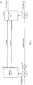
- FIG. 1 shows an example of a system on a chip (SoC) 110 with a memory interface for interfacing one or more blocks (e.g., CPU, GPU, etc.) on the SoC 110 with an external memory device (e.g., double data rate synchronous dynamic random access memory (DDR SDRAM)).
- SoC system on a chip
- an external memory device e.g., double data rate synchronous dynamic random access memory (DDR SDRAM)
- DDR SDRAM double data rate synchronous dynamic random access memory
- the memory interface comprises a centrally-located memory controller 115, and a plurality of physical (PHY) blocks 120a-120e and 125a-125e located along the periphery of the SoC 110.
- the memory controller 115 manages the flow of data between the external DDR SDRAM and a block on the SoC 110 that needs to access the external DDR SDRAM. Memory access may include writing data to and reading data from the external DDR SDRAM. For example, when a block on the SoC 110 needs to write data to the external DDR SDRAM, the memory controller 115 generates and sends the corresponding DDR data, clock signal and command/address (CA) signal to one or more of the PHY blocks 120a-120e and 125a-125e.
- the one or more PHY blocks 120a-120e and 125a-125e condition the DDR data, clock signal and CA signal for output to the external DDR SDRAM in accordance with an applicable memory standard.
- the DDR data may have a width of four bytes corresponding to a four-byte data word.
- the memory controller 115 sends four bytes of the DDR data in parallel to four of the PHY blocks (e.g., PHY blocks 120a-120d), in which each byte is sent to a different one of the four PHY blocks.
- the memory controller 115 also sends the clock signal to each of the four PHY blocks.
- each of the four PHY blocks receives the respective byte of the DDR data and the clock signal.
- the memory controller 115 also sends the CA signal to a fifth one of the PHY blocks (e.g., PHY block 120e) for output to the external DDR SDRAM.
- the SoC 110 has two memory channels (denoted CH0 and CH1) for transferring DDR data to the same memory device or different memory devices.
- the memory controller 115 may send DDR data and a CA signal for channel CH0 to PHY blocks 120a-120e.
- the DDR data for channel CH0 may have a width of four bytes (denoted DQ0, DQ1, DQ2 and DQ3), in which each byte is sent to a respective one of the PHY blocks 120a-120d.
- the CA signal for channel CH0 is sent to PHY block 120e.
- the memory controller 115 may send DDR data and a CA signal for channel CH1 to PHY blocks 125a-125e.
- the DDR data for CH1 may have a width of four bytes (denoted DQ0, DQ1, DQ2 and DQ3), in which each byte is sent to a respective one of the PHY blocks 125a-125d.
- the CA signal for channel CH0 is sent to PHY block 125e.
- Interfacing with the DDR SDRAM can be extremely challenging due to high speeds, which translate into tight timing requirements that need to be met between the SoC and the DDR SDRAM.
- One challenge is distributing the centrally-generated DDR data and clock signal for the different bytes all the way to the corresponding PHY blocks on the periphery on the SoC.
- the PHY blocks may be spaced far apart along the periphery of the SoC.
- the different bytes of the DDR data and the clock signal have to traverse different paths to the periphery of the SoC over relatively long distances (e.g., 10 to 20 millimeters).
- Another approach for sending data across the SoC is to use a standard asynchronous clock domain crossing circuit such as a first-in-first-out (FIFO) device.
- a standard asynchronous clock domain crossing circuit such as a first-in-first-out (FIFO) device.
- FIFO first-in-first-out
- This approach incurs several additional clock cycles for the domain crossing, which can be a huge penalty for a latency-sensitive system.
- This approach also requires coordination between the PHY blocks to make sure that bytes corresponding to the same word of the DDR data are aligned when they are output to the external DDR SDRAM.
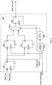
- FIG. 2 shows a memory interface 205 according to an aspect of the present disclosure.
- the memory interface 205 comprises the memory controller 115 and a clock phase-locked loop (PLL) 210, both of which may be centrally located on the SoC 110.
- the memory interface 205 also comprises a cleanup PLL 225 and a synchronization circuit 230, both of which are located near the periphery of the SoC 110 and may be included in one of the PHY blocks shown in FIG. 1 .
- the memory interface 205 may also comprise a frequency divider 212.
- the clock PLL 210 receives an input clock signal from a crystal oscillator (not shown), and generates an output clock signal based on the input clock signal.
- the memory controller 115 generates DDR data based on data from a block (not shown) on the SoC 110 accessing the external DDR SDRAM.
- the memory controller 115 also generates a data clock signal based on the output clock signal from the clock PLL 210.
- the data clock signal may have a frequency of about one gigahertz or more.
- the memory controller 115 outputs the DDR data and the data clock signal to the synchronization circuit 230.
- the DDR data may be aligned with rising edges of the data clock signal at the memory controller 115.
- the DDR data and the data clock signal may travel over a relatively long distance (e.g., 10 to 20 millimeters) across the SoC 110 from approximately the center of the SoC 110 to the synchronization circuit 230, which is located near the periphery of the SoC 110.
- a relatively long distance e.g. 10 to 20 millimeters
- the frequency divider 212 also receives the output clock signal from the clock PLL 210, and divides the frequency of the output clock signal by N to generate a lower-frequency reference clock signal, which is output to the cleanup PLL 225.
- the frequency reduction is done to reduce power consumption since a lower frequency clock signal consumes less power.
- the reference clock signal travels over a relatively long distance (e.g., 10 to 20 millimeters) across the SoC 110 from approximately the center of the SoC 110 to the cleanup PLL 225, which is located near the periphery of the SoC 110. As a result, the reference clock signal accumulates jitter from various parts of the SoC by the time the reference clock signal reaches the cleanup PLL 225.
- the cleanup PLL 225 reduces the jitter in the reference clock signal and multiples up the frequency of the reference clock signal by N to produce a clean clock signal.
- the clean clock signal may have the same frequency as the data clock signal, but not necessarily the same phase.
- the cleanup PLL 225 reduces jitter using a loop filter (e.g., a low-pass loop filter) that attenuates the jitter.
- the clean clock signal may be used for a DDR output clock signal that is output to the external DDR SDRAM. This is because the clean clock signal (which is generated near the periphery of the SoC 110) only has to travel a short distance to reach an IO pin of the SoC 110 for output to the external DDR SDRAM, and therefore has low jitter.
- the clean clock signal may also be used to generate a data strobe signal to the DDR SDRAM, which the DDR SDRAM may use to sample (capture) the DDR data.
- the low jitter makes it easier to meet clock and data strobe timing requirements to the DDR SDRAM.
- the synchronization circuit 230 receives the DDR data and data clock signal from the memory controller 115 and the clean clock signal from the cleanup PLL 225, which is located near the synchronization circuit 230 and is therefore local to the synchronization circuit 230.
- the synchronization circuit 230 samples (captures) the DDR data using the data clock signal. For example, the synchronization circuit 230 may capture DDR data on the rising or falling edges of the data clock signal.
- the synchronization circuit 230 then synchronizes the captured DDR data with the clean clock signal.
- the synchronization circuit 230 retimes the DDR data from the data clock domain to the clean clock domain.
- the synchronization circuit 230 may output the retimed DDR data to the external DDR SDRAM.
- the retimed DDR data may be output directly to the external DDR SDRAM via one or more IO pins on the SoC 110, or may undergo additional processing at the respective PHY block before being output to the external DDR SDRAM via the one or more IO pins.
- each of the PHY blocks shown in FIG. 1 may include one or more synchronization circuits and one or more cleanup PLLs.
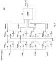
- FIG. 3 shows a synchronization circuit 330 according to one embodiment of the present disclosure.
- the synchronization circuit 330 comprises a first-stage flip-flop 335, a rising-edge (RE) flip-flop 340, a falling-edge (FE) flip-flop 350, an output flip-flip 365, a multiplexer 360, a phase detector 370, and a selector 380.
- RE rising-edge
- FE falling-edge
- the first-stage flip-flop 335 receives DDR data and the data clock signal from the memory controller 115, and samples (captures) the DDR data on the falling edges of the data clock signal.
- the first-stage flip-flop 335 outputs the sampled (captured) DDR data to the RE flip-flop 340 and the FE flip-flip 350.
- the RE flip-flop 340 samples the DDR data from the first-stage flip-flop 335 on the rising edges of the clean clock signal
- the FE flip-flop 350 samples the DDR data from the first-stage flip-flop 335 on the falling edges of the clean clock signal.
- the RE flip-flop 340 and the FE flip-flip 350 output the RE-sampled DDR data and the FE-sampled DDR data, respectively, to the multiplexer 360.
- the multiplexer 360 selectively outputs the RE-sampled DDR data or the FE-sampled DDR data to the output flip-flop 365 based on commands from the selector 380, as discussed further below.
- the output flip-flop 365 samples (captures) the output of the multiplexer 360 on the falling edges of the clean clock signal to produce clean DDR data that is aligned with the clean clock signal.
- the synchronization circuit 330 retimes the DDR data from the data clock domain to the clean clock domain.
- the clean clock signal may be used for the DDR clock output to the DDR SDRAM, in which case, the synchronization circuit 330 synchronizes the DDR data with the DDR clock output.
- the clean clock signal from the cleanup PLL 225 and the data clock signal may have the same frequency, but not necessarily the same phase.
- the phase detector 370 receives the clean clock signal and the data clock signal, and determines the phase difference (offset) between the two clock signals.
- the granularity of the phase detection may be a quarter of a clock cycle (period) or finer granularity.
- the selector 380 commands the multiplexer 360 to select the RE-sampled DDR data from the RE flip-flop 340 or the FE-sampled DDR data from the FE flip-flop 350 based on the phase detection from the phase detector 370, as discussed further below.
- the selector 380 determines whether a falling edge (sampling edge) of the data clock signal is closer to a rising edge or a falling edge of the clean clock signal based on the phase detection from the phase detection 370. If the falling edge (sampling edge) of the data clock signal is closer to the rising edge of the clean clock signal, then the selector 380 commands the multiplexer 360 to select the FE-sampled DDR data from the FE flip-flop 350. If the falling edge (sampling edge) of the data clock signal is closer to the falling edge of the clean clock signal, then the selector 380 commands the multiplexer 360 to select the RE-sampled DDR data from the RE flip-flop 340.
- the selector 380 selects the output of the flip-flop 340 and 350 that samples the DDR data on an edge of the clean clock signal that is farther away from the falling edge (sampling edge) of the data clock signal. This is because the DDR data from the first-stage flip-flop 335 changes on the falling edges (sampling edges) of the data clock signal. As a result, the DDR data from the first-stage flip-flop 335 is more likely to be stable (and therefore less likely to cause a metastable state) when sampled on an edge of the clean clock signal that is farther away from the falling edge (sampling edge) of the data clock signal.
- the granularity of the phase detector 370 is a quarter of a clock cycle (period).
- FIG. 4 shows an example of a clean clock signal 410, in which each cycle of the clean clock signal 410 is divided into four quadrants (labeled one to four).
- the phase detector 370 may output a value indicating in which of the four quadrants of the clean clock signal 410 a falling edge (sampling edge) of the data clock signal lies. If the phase detector 370 indicates that the falling edge of the data clock signal lies in quadrant one or quadrant four, then the falling edge of the data clock signal may be considered to be closer to a rising edge of the clean clock signal 410 than a falling edge of the clean clock signal 410.
- the selector 380 may command the multiplexer 360 to select the FE-sampled DDR data from the FE flip-flop 350. If the phase detector 370 indicates that the falling edge of the data clock signal lies in quadrant two or quadrant three, then the falling edge of the data clock signal may be considered to be closer to a falling edge of the clean clock signal 410 than a rising edge of the clean clock signal 410. In this case, the selector 380 may command the multiplexer 360 to select the RE-sampled DDR data from the RE flip-flop 340.
- FIG. 5 shows a synchronization circuit 530 according to another embodiment, in which the phase detector 570 performs phase detection using a calibration signal from the memory controller 115.
- the memory controller 115 may periodically output a calibration signal to the synchronization circuit 530.
- the memory controller 115 may output a calibration signal once every M number of cycles of the data clock signal.
- Each calibration signal may comprise a pulse signal or other type of signal.
- the memory controller 115 may periodically output a calibration signal on a data line used to transport DDR data from the memory controller 115 to the synchronization circuit 530, in which DDR data and the calibration signal are sent at different times on the data line.
- the first-stage flip-flop 335 captures the calibration signal on a falling edge (sampling edge) of the data clock signal. As a result, the rising edge of the captured calibration signal is approximately aligned with the falling edge (sampling edge) of the data clock signal.
- the phase detector 570 receives the captured calibration signal from the first-stage flip-flop 335 and determines the phase difference (offset) between the rising edge of the captured calibration signal and a rising edge of the clean clock signal.
- the phase difference is approximately equal to the phase difference between the falling edge (sampling edge) of the data clock signal and the rising edge of the clean clock signal.
- the phase detector 570 outputs the determined phase difference to the selector 380, which commands the multiplexer 360 to select the RE-sampled DDR data from the RE flip-flop 340 or the FE-sampled DDR data from the FE flip-flop 350 based on the phase difference. For example, if the phase detector 570 has a granularity of a quarter of a clock cycle, then the selector 380 may command the multiplexer 360 to select the RE-sampled DDR data from the RE flip-flop 340 when the phase detector 570 indicates that the rising edge of the captured calibration signal lies in quadrant two or three. The selector 380 may command the multiplexer 360 to select the FE-sampled DDR data from the FR flip-flop 350 when the phase detector 570 indicates that the rising edge of the captured calibration signal lies in quadrant one or four.
- the selector 380 commands the multiplexer 360 to select the RE flip-flop 340 or the FE flip-flop 350 based on the phase detection using the most recently received calibration signal.
- the selection is only updated when a calibration signal is received from the memory controller 115 and remains constant between calibration signals.
- the frequency of phase detections (and hence selector updates) can be controlled by controlling the frequency of calibration signals.
- the frequency of the calibration signals can be controlled and fine-tuned based on characterization of jitter in the SoC 110.
- FIG. 6 shows an exemplary implementation of the phase detector 570 according to an aspect of the present disclosure.
- the phase detector 570 has a granularity of a quarter of a clock cycle.
- the phase detector 570 comprises a first input flip-flip 610-1, a second input flip-flop 610-2, a third input flip-flop 610-3, a fourth input flip-flop 610-2, a first output flip-flop 620-1, a second output flip-flop 620-2, a third output flip-flop 620-3, a fourth output flip-flop 610-4, and an encoder 630.
- Each of the first, second, third and fourth input flip-flops 610-1 to 610-4 receives a calibration signal from the output of the first-stage flip-flop 335 at its data input D.
- the first input flip-flop 610-1 receives the clean clock signal at its clock input Clk
- the second input flip-flop 610-2 receives the clean clock signal shifted by 90 degrees at its clock input Clk
- the third input flip-flop 610-3 the clean clock signal shifted by 180 degrees at its clock input Clk
- the fourth input flip-flop 610-4 receives the clean clock signal shifted by 270 degrees at its clock input Clk.
- the first input flip-flop 610 samples the calibration signal on a rising edge of the clean clock signal
- the second input flip-flop 610-2 samples the calibration signal on a rising edge of the clean clock signal shifted by 90 degrees
- the third input flip-flop 610-3 samples the calibration signal on a rising edge of the clean clock signal shifted by 180 degrees
- the fourth input flip-flop 610-4 samples the calibration signal on a rising edge of the clean clock signal shifted by 270 degrees.
- the first, second, third and fourth input flip-flops 610-1 to 610-4 sample the calibration signal at four different sample points spaced 90 degrees apart from one another.
- Each of the output flip-flops 620-1 to 620-4 is coupled to the output of a respective one of the input flip-flops 610-1 to 610-4.
- the first output flip-flop 620-1 is coupled to the output of the first input flip-flop 610-1
- the second output flip-flop 620-2 is coupled to the output of the second input flip-flop 610-2
- Each of the output flip-flops 620-1 to 620-4 samples (captures) the output value of the respective input flip-flop 610-1 to 610-4 on a rising edge of the clean clock signal and outputs the sampled output value to the encoder 630.
- the encoder 630 receives four values (denoted Dsamp[0] to Dsamp [3] in FIG. 6 ), where each value corresponds to the calibration signal sampled at a different one of the four sample points.
- the encoder 630 determines in which quadrant the rising edge of the calibration signal lies based on the four values from the output flip-flops 620-1 to 620-4, and outputs a phase-detection signal indicating the determined quadrant to the selector 380.
- the phase-detection signal may be a two-bit signal (denoted Pout[1:0] in FIG. 6 ) identifying the quadrant in which the rising edge of the calibration signal lies.
- FIG. 7 shows an example of the clean clock signal 710, in which each clock cycle is divided into four quadrants.
- FIG. 7 also shows four sample points ph0, ph90, ph180 and ph270 corresponding to the first, second, third and fourth input flip-flops 610-1, 610-2, 610-3 and 610-4, respectively.
- FIG. 7 further shows four exemplary calibration signals 720-1 to 720-4, in which each calibration signal has a rising edge lying in a different quadrant of the clean clock signal 710, and each calibration signal has a pulse width equal to approximately one clock cycle.
- FIG. 7 shows the four output values from the first, second, third and fourth input flip-flops 610-1 to 610-4 for that calibration signal.
- the first input flip-flop 610-1 outputs a logic zero
- each of the second, third and fourth input flip-flops 610-2, 610-3 and 610-4 outputs a logic one (represented by "0111" on the waveform of the calibration signal 720-1).
- each of the first and second input flip-flops 610-1 and 610-2 outputs a logic zero
- each of the third and fourth input flip-flops 610-3 and 610-4 outputs a logic one (represented by "0011" on the waveform of the calibration signal 720-2).
- each of the first, second and third input flip-flops 610-1, 610-2 and 610-3 outputs a logic one
- the fourth input flip-flop 610-4 outputs a logic zero (represented by "1110" on the waveform of the calibration signal 720-3).
- each of the first, second, third and fourth input flip-flops 610-1 to 610-4 outputs a logic one (represented by "1111" on the waveform of the calibration signal 720-4).
- the encoder 630 may be programmed to determine in which quadrant the rising edge of a calibration signal lies according to the output values given above for each quadrant.
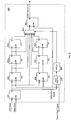
- FIG. 8 shows a synchronization circuit 830 according to another embodiment of the present disclosure.
- the synchronization circuit 830 is similar to the one shown in FIG. 5 , except the synchronization circuit 830 comprises first, second and third RE flip-flops 840, 842 and 844, and first, second and third FE flip-flops 850, 852 and 854.
- the first, second and third RE flip-flops 844, 842 and 842 are coupled in series.
- the first RE flip-flop 840 samples the output of the first-stage flip-flop 335 on the rising edges of the clean clock signal
- the second RE flip-flop 842 samples the output of the first RE flip-flop 840 on the rising edges of the clean clock signal
- the third RE flip-flop 844 samples the output of the second RE flip-flop 842 on the rising edges of the clean clock signal.
- the first, second and third FE flip-flops 854, 852 and 854 are coupled in series.
- the first FE flip-flop 850 samples the output of the first-stage flip-flop 335 on the falling edges of the clean clock signal
- the second FE flip-flop 852 samples the output of the first FE flip-flop 850 on the falling edges of the clean clock signal
- the third FE flip-flop 854 samples the output of the second FE flip-flop 852 on the falling edges of the clean clock signal.
- the input of the multiplexer 860 is coupled to the outputs of the RE flip-flops 840, 842 and 844, the outputs of the FE flip-flops 850, 852 and 854, and the output of the first-stage flip-flop 335.
- the selector 880 commands the multiplexer 360 to select the output of one of the flip-flops based on phase-detection signals from the phase detector 570.
- the multiplexer 360 couples the selected output to the output flip-flop 365, which samples (captures) the selected output on the falling edges of the clean clock signal to produce DDR data that is synchronized with the clean clock signal (which may be used for the DDR clock output).
- the flip-flops 335, 840,842, 844, 850, 852 and 854 provide sampled data corresponding to seven different sample points.
- the sample points of the first, second and third RE flip-flops 840, 842 and 844 are offset by one clock cycle from one another.
- the sample points of first, second and third FE flip-flops 850, 852 and 854 are offset by one clock cycle from one another, and offset by half a clock cycle from the sample points of the first, second and third RE flip-flops 840, 842 and 844.
- the selector 880 selects the sample point corresponding to the selected flip-flop.
- the synchronization circuit 830 is able to prevent cycle slips between different PHY blocks.
- a cycle slip may occur when two data bytes corresponding to the same clock cycle at the memory controller 115 are sampled (captured) at different clock cycles at the respective PHY blocks. As a result, two data bytes that are aligned at the memory controller 115 are no longer aligned at the PHY blocks.
- the synchronization circuit 830 is able to prevent a cycle slip by pulling in or pushing out the output of the synchronization circuit 830, as discussed further below.
- a cycle slip may be caused when the phase difference between the data clock signal and the clean clock signal drifts over time at one PHY block, but not at another PHY block or drifts by a different amount at another PHY block.
- the phase drift may be caused by temperature changes in the SoC and/or another cause.
- a static cycle slip may be caused by static delay mismatches between the memory controller 115 and different PHY blocks.
- the synchronization circuit 830 is able to prevent both types of cycle slips.
- the selector 880 may be configured to detect the phase drift between calibration signals from the memory controller 115 and the clean clock signal, and adjust the selection of the multiplexer 360 accordingly to compensate for the detected drift. If the phase drift is gradual, then the selector 880 may detect the drift by tracking changes in the phase-detection signals from the phase detector 570 over time.
- the selector 880 may detect the phase drift by tracking changes in the quadrant indicated by the phase-detection signals. Assuming the phase drift is less than 90 degrees between phase-detection signals, the selector 880 can determine the direction of the phase drift based on changes in the quadrant indicated by the phase-detection signals. The selector 880 may then adjust the flip-flop selection by the multiplexer 360 to compensate for the detected phase drift, thereby preventing a cycle slip.
- the selector 880 may be implemented using a truth table 905, an example of which is shown in FIG. 9 .
- each row corresponds to a quadrant and each column corresponds to a different one of the flip-flops from which the multiplexer 860 can choose.
- the first, second and third RE flip-flops 840, 842 and 844 are represented by RE0, RE1 and RE2, respectively, in the truth table 905.
- the first, second and third FE flip-flops 850, 852 and 854 are represented by FE0, FE1 and FE2, respectively, in the truth table 905.
- the first-stage flip-flop 335 is represented by "Launch" in the truth table 905 since the output of the first-stage flip-flop 335 is a data launch point in the synchronization circuit 830.
- each quadrant is annotated with a (n), (n+1) or (n-1). This is used to distinguish quadrants corresponding to different amounts of phase drift.
- quadrant 4(n+1) may correspond to a phase drift of one clock cycle from quadrant 4(n) in one direction
- quadrant 4(n-1) may correspond to a phase drift of one clock cycle from quadrant 4(n) in the opposite direction.
- the selector 880 may start at a certain entry in the truth table 905, and select one of the flip-flops based on the starting entry.
- the phase detector 570 may initially output a phase-detection signal indicating quadrant one.
- the selector 800 may start at the entry corresponding to quadrant 1(n) in the truth table 905 and select the output of the first FE flip-flop 850.
- the selector 880 can update the flip-flop selection using the truth table 905 to compensate for phase drift, as discussed further below.
- the selector 880 moves to the entry corresponding quadrant 2(n) in the truth table 905 and selects the output of the first RE flip-flop 840.
- the selector 880 moves to the entry corresponding to quadrant 3(n+1) in the truth table 905. In this case, the flip-flop selection does not change.
- the selector 880 moves to the entry corresponding to quadrant 4(n+1) and selects the output of the first-stage flip-flop 335.
- the quadrant changes due to phase drift causes the selector 380 to move to the right of the truth table 905, and therefore pull in the output of the selector 380 to compensate for the phase drift.
- the selector 880 moves to the entry corresponding quadrant 4(n) in the truth table 905. In this case, the flip-flop selection does not change.
- the selector 880 moves to the entry corresponding to quadrant 3(n) in the truth table 905 and selects the output of the second RE flip-flop 852.
- the selector 880 moves to the entry corresponding to quadrant 2(n-1). In this case the flip-flop selection is not changed.
- the selector 880 moves to the entry corresponding to quadrant 1(n-1) in the truth table 905 and selects the output of the second FE flip-flop 852.
- the quadrant changes due to phase drift causes the selector 380 to move to the left of the truth table 905, and therefore push out the output of the selector 380 to compensate for the phase drift.
- the truth table 905 can be used to adjust the flip-flop selection by the multiplexer 860 to compensate for phase drift in either direction.
- the starting entry corresponds to quadrant 1(n) in the truth table 905 in the example discussed above, it is to be appreciated that embodiments of the present disclosure are not limited to this example.
- the phase detector 570 may initially output a phase-detection signal indicating quadrant four.
- the selector 880 may use the entry corresponding to quadrant 4(n) in the truth table 905 as the starting point.
- the starting entry may depend on the initial quadrant indicated by the phase detector 570.
- embodiments of the present disclosure are not limited to the particular truth-table entries shown in the FIG. 9 .
- a static cycle slip may be caused by static delay mismatches between the memory controller 115 and different PHY blocks (e.g., mismatches in the lengths of the signal paths from the memory controller 115 to the different PHY blocks).
- static cycle slip two data bytes that are in the same cycle at the memory controller 115 may end up in different cycles at the PHY blocks.
- each of the PHY blocks may include the synchronization circuit 830 shown in FIG. 8 .
- the memory controller 115 sends a calibration signal to each of the PHY blocks.
- the phase detector 570 at each of the PHY blocks determines in which quadrant of the DDR clock signal the respective calibration signal is aligned.
- Each PHY block may then report the determined quadrant to the memory controller 115 or another controller. If each of the PHY blocks reports the same quadrant, then the memory controller 115 may do nothing. However, if the PHY blocks report different quadrants, then static delay mismatch is evident. In this case, the memory controller 115 may analyze the different quadrants reported by the PHY blocks to determine whether the static mismatch results in is a static cycle slip, and if so determine how to calibrate out the static cycle slip.
- FIG. 10 shows an example of the quadrants reported by three PHY blocks.
- a first one of the PHY blocks is used for the CA signal, a second one of the PHY blocks is used for data byte DQ0, and a third one of the PHY blocks is used for data byte DQ1.
- the first PHY block is aligned in quadrant one
- the second PHY block is aligned in quadrant two
- the third PHY block is aligned quadrant three.
- the up arrow on the DDR clock signal indicates the alignment of the outputs of the PHY blocks.
- the outputs of the PHY blocks are aligned and a static cycle slip correction is not needed.
- FIG. 11 shows an example in which the first PHY block is aligned in quadrant two, the second PHY block is aligned in quadrant three, and the third PHY block is aligned quadrant four.
- the outputs of the PHY blocks are also aligned.
- FIG. 12 shows an example in which the first PHY block is aligned in quadrant three, the second PHY block is aligned in quadrant four, and the third PHY block is aligned quadrant one.
- the outputs of the first and second PHY blocks are aligned.
- the output of third PHY block is offset from the outputs of the first and second PHY blocks by one clock cycle, resulting in a static cycle slip.
- the static cycle slip can be corrected by pulling in the output of the third PHY blocks by one clock cycle to align with the outputs of the first and second PHY blocks.
- the static cycle slip may be corrected by pushing out the outputs of the first and second PHY blocks by one clock cycle to align with the output of the third PHY block.
- the memory controller 115 may send instructions to the first and second PHY blocks to push out by one clock cycle to correct the static cycle slip.
- the synchronization circuit 830 in each of the first and second PHY blocks may then push out the respective output by one clock cycle by changing the flip-flop selection by the respective multiplexer 860. For example, if the first FE flip-flop 850 is initially selected, then the synchronization circuit 830 may push out by one clock cycle by shifting to the second FE flip-flop 852, which is delayed by one clock cycle from the first FE flip-flop 850.
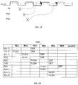
- FIG. 13 shows a truth table 1305 according to one embodiment.
- the truth table 1305 includes a set of default entries (labeled "DEF") and a set of push-out entries (labeled "PUSH").
- the DEF entries correspond to a default condition and the PUSH entries correspond to a push out of one clock cycle from the default condition.
- PHY blocks that are not pushed out perform flip-flop selection using the DEF entries in the truth table
- PHY blocks that are pushed out to correct a static cycle slip perform flip-flop selection using the PUSH entries in the truth table 1305.
- the synchronization circuits 830 in the first and second PHY blocks may use the PUSH entries to perform flip-flop selection since they are instructed to push out.
- the synchronization circuit 830 in the third PHY block may use the DEF entries to perform flip-flop selection.
- FIG. 14 shows an example in which the first PHY block is aligned in quadrant four, the second PHY block is aligned in quadrant one, and the third PHY block is aligned in quadrant two.
- the outputs of the second and third PHY blocks are aligned.
- the output of the first PHY block is offset from the outputs of the second and third PHY blocks by one clock cycle, resulting in a static cycle slip.
- the static cycle slip can be corrected by pulling in the outputs of the second and third PHY blocks by one clock cycle to align with the output of the first block PHY block.
- the static cycle slip may be corrected by pushing out the output of the first PHY block by one clock cycle to align with the outputs of the second and third PHY blocks.
- the memory controller 115 may send instructions to the first PHY block to push out by one clock cycle to correct the static cycle slip.
- FIG. 15 shows a truth table 1505 according to one embodiment.
- the truth table 1505 includes a set of default entries (labeled "DEF") and a set of push-out entries (labeled "PUSH").
- PHY blocks that are not pushed out perform flip-flop selection using the DEF entries in the truth table 1505
- PHY blocks that are pushed out to correct a static cycle slip perform flip-flop selection using the PUSH entries in the truth table 1505.
- the synchronization circuit 830 in the first PHY block may use the PUSH entries to perform flip-flop selection
- the synchronization circuits 830 in the second and third PHY blocks may use the DEF entries to perform flip-flop selection.
- the methodology for correcting static cycle drift is not limited to the particular examples given above.
- the memory controller 115 may output a plurality of calibration signals to each PHY block.
- each PHY block may determine a quadrant for each of the calibration signals, and report the quadrant that is determined the most for the calibration signals to the memory controller 115.
- the memory controller 115 may instruct one or more PHY blocks to pull in by one clock cycle to correct a detected static cycle slip.
- the truth table may include pull-in (PULL) entries located to the right of the DEF entries in the truth table, and a PHY block that is instructed to pull in may use the PULL entries for performing flip-flop selection.
- the static cycle slip shown in the example in FIG. 12 may be corrected by pulling in the third PHY block by one clock cycle so that the output of the third PHY block aligns with the outputs of the first and second PHY blocks.
- the third PHY block may use the PULL entries and the first and second PHY blocks may use the DEF entries.
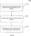
- FIG. 16 is a flow diagram of a method 1600 for synchronizing data according to an embodiment of the present disclosure.
- the method 1600 may be performed at a PHY block located near a periphery of the SoC to retime data from the memory controller 115 with a clean clock signal, which may be used as a clock output (e.g., DDR clock output) to an external memory (e.g., DDR SDRAM).
- a clock output e.g., DDR clock output
- an external memory e.g., DDR SDRAM
- a clean clock signal is generated based on a reference clock signal.
- the clean clock signal may be generated by a phase-locked loop (PLL) (e.g., cleanup PLL 225) that attenuates jitter in the reference clock signal.
- PLL phase-locked loop
- step 1620 data is sampled using a data clock signal.
- the data and the data clock signal may be sent from a memory controller (e.g., memory controller 115), and may travel a relative long distance across the SoC from the memory controller (which may be centrally-located on the SoC) to the periphery of the SoC.
- the data may be sampled using a flip-flop (e.g., the input flip-flop) that samples (captures) the data on the rising edges or falling edges of the data clock signal.
- the sampled data is synchronized with the clean clock signal.
- the sampled data may be sampled by one or more flip-flops that are clocked using the clean clock signal (e.g., or more of flip-flops 840, 842, 844, 850, 852, 854 and 365).
- the first-stage flip-flop may sample the DDR data on the rising edges of the data clock signal.
- the sampling edges of the first-stage flip-flop would correspond to the rising edges of the data clock signal.
- the synchronization circuit 830 may comprise any number of RE flip-flops and any number of FE flip-flops.
- the number of RE flip-flops and FE flip-flops may be increased to allow the synchronization circuit to correct for phased drifts over a wider range, if needed.
- the truth table may be expanded to include entries for the additional RE flip-flops and FE flip-flops.
- DSP digital signal processor
- ASIC application specific integrated circuit
- FPGA field programmable gate array
- a general-purpose processor may be a microprocessor, but in the alternative, the processor may be any conventional processor, controller, microcontroller, or state machine.
- a processor may also be implemented as a combination of computing devices, e.g., a combination of a DSP and a microprocessor, a plurality of microprocessors, one or more microprocessors in conjunction with a DSP core, or any other such configuration.
- a software module may reside in RAM memory, flash memory, ROM memory, EPROM memory, EEPROM memory, registers, hard disk, a removable disk, a CD-ROM, or any other form of storage medium known in the art.
- An exemplary storage medium is coupled to the processor such that the processor can read information from, and write information to, the storage medium.
- the storage medium may be integral to the processor.
- the processor and the storage medium may reside in an ASIC.
- the ASIC may reside in a user terminal.
- the processor and the storage medium may reside as discrete components in a user terminal.
- the functions described may be implemented in hardware, software, firmware, or any combination thereof. If implemented in software, the functions may be stored on or transmitted over as one or more instructions or code on a computer-readable medium.
- Computer-readable media includes both computer storage media and communication media including any medium that facilitates transfer of a computer program from one place to another.
- a storage media may be any available media that can be accessed by a general purpose or special purpose computer.
- such computer-readable media can comprise RAM, ROM, EEPROM, CD-ROM or other optical disk storage, magnetic disk storage or other magnetic storage devices, or any other medium that can be used to carry or store desired program code means in the form of instructions or data structures and that can be accessed by a general-purpose or special-purpose computer, or a general-purpose or special-purpose processor.
- any connection may be properly termed a computer-readable medium to the extent involving non-transient storage of transmitted signals.
- Disk and disc includes compact disc (CD), laser disc, optical disc, digital versatile disc (DVD), floppy disk and blu-ray disc where disks usually reproduce data magnetically, while discs reproduce data optically with lasers. Combinations of the above should also be included within the scope of computer-readable media.
Landscapes
- Engineering & Computer Science (AREA)
- Theoretical Computer Science (AREA)
- Microelectronics & Electronic Packaging (AREA)
- Computer Hardware Design (AREA)
- Physics & Mathematics (AREA)
- General Engineering & Computer Science (AREA)
- General Physics & Mathematics (AREA)
- Synchronisation In Digital Transmission Systems (AREA)
- Stabilization Of Oscillater, Synchronisation, Frequency Synthesizers (AREA)
Applications Claiming Priority (2)
| Application Number | Priority Date | Filing Date | Title |
|---|---|---|---|
| US13/902,705 US9123408B2 (en) | 2013-05-24 | 2013-05-24 | Low latency synchronization scheme for mesochronous DDR system |
| PCT/US2014/000141 WO2014189551A1 (en) | 2013-05-24 | 2014-06-02 | Low latency synchronization scheme for mesochronous ddr system |
Publications (2)
| Publication Number | Publication Date |
|---|---|
| EP3028161A1 EP3028161A1 (en) | 2016-06-08 |
| EP3028161B1 true EP3028161B1 (en) | 2018-07-18 |
Family
ID=51298925
Family Applications (1)
| Application Number | Title | Priority Date | Filing Date |
|---|---|---|---|
| EP14748318.4A Active EP3028161B1 (en) | 2013-05-24 | 2014-06-02 | Low latency synchronization scheme for mesochronous ddr system |
Country Status (5)
| Country | Link |
|---|---|
| US (2) | US9123408B2 (enExample) |
| EP (1) | EP3028161B1 (enExample) |
| JP (1) | JP6306160B2 (enExample) |
| KR (1) | KR20160040140A (enExample) |
| WO (1) | WO2014189551A1 (enExample) |
Families Citing this family (38)
| Publication number | Priority date | Publication date | Assignee | Title |
|---|---|---|---|---|
| US8760945B2 (en) * | 2011-03-28 | 2014-06-24 | Samsung Electronics Co., Ltd. | Memory devices, systems and methods employing command/address calibration |
| US9123408B2 (en) | 2013-05-24 | 2015-09-01 | Qualcomm Incorporated | Low latency synchronization scheme for mesochronous DDR system |
| KR20150040540A (ko) * | 2013-10-07 | 2015-04-15 | 에스케이하이닉스 주식회사 | 반도체 장치 및 이를 포함하는 반도체 시스템 |
| US9478268B2 (en) * | 2014-06-12 | 2016-10-25 | Qualcomm Incorporated | Distributed clock synchronization |
| US9495285B2 (en) | 2014-09-16 | 2016-11-15 | Integrated Device Technology, Inc. | Initiating operation of a timing device using a read only memory (ROM) or a one time programmable non volatile memory (OTP NVM) |
| US9209961B1 (en) * | 2014-09-29 | 2015-12-08 | Apple Inc. | Method and apparatus for delay compensation in data transmission |
| US10187067B2 (en) * | 2014-10-14 | 2019-01-22 | Qatar University | Phase-locked loop (PLL)-type resolver/converter method and apparatus |
| US9553570B1 (en) | 2014-12-10 | 2017-01-24 | Integrated Device Technology, Inc. | Crystal-less jitter attenuator |
| US9324397B1 (en) * | 2015-01-16 | 2016-04-26 | Qualcomm Incorporated | Common die for supporting different external memory types with minimal packaging complexity |
| US9369139B1 (en) | 2015-02-14 | 2016-06-14 | Integrated Device Technology, Inc. | Fractional reference-injection PLL |
| US9336896B1 (en) | 2015-03-23 | 2016-05-10 | Integrated Device Technology, Inc. | System and method for voltage regulation of one-time-programmable (OTP) memory programming voltage |
| US9455045B1 (en) | 2015-04-20 | 2016-09-27 | Integrated Device Technology, Inc. | Controlling operation of a timing device using an OTP NVM to store timing device configurations in a RAM |
| US9362924B1 (en) * | 2015-07-08 | 2016-06-07 | Integrated Device Technology, Inc. | Method and apparatus for fast frequency acquisition in PLL system |
| US9362928B1 (en) | 2015-07-08 | 2016-06-07 | Integrated Device Technology, Inc. | Low-spurious fractional N-frequency divider and method of use |
| US9954516B1 (en) | 2015-08-19 | 2018-04-24 | Integrated Device Technology, Inc. | Timing device having multi-purpose pin with proactive function |
| US9590637B1 (en) | 2015-08-28 | 2017-03-07 | Integrated Device Technology, Inc. | High-speed programmable frequency divider with 50% output duty cycle |
| JP6584885B2 (ja) * | 2015-09-14 | 2019-10-02 | 株式会社東芝 | 雑音除去機能を有する機器 |
| US9847869B1 (en) | 2015-10-23 | 2017-12-19 | Integrated Device Technology, Inc. | Frequency synthesizer with microcode control |
| US9614508B1 (en) | 2015-12-03 | 2017-04-04 | Integrated Device Technology, Inc. | System and method for deskewing output clock signals |
| US9893877B2 (en) * | 2016-01-15 | 2018-02-13 | Analog Devices Global | Circuits, systems, and methods for synchronization of sampling and sample rate setting |
| US10075284B1 (en) | 2016-01-21 | 2018-09-11 | Integrated Device Technology, Inc. | Pulse width modulation (PWM) to align clocks across multiple separated cards within a communication system |
| US9852039B1 (en) | 2016-02-03 | 2017-12-26 | Integrated Device Technology, Inc | Phase locked loop (PLL) timing device evaluation system and method for evaluating PLL timing devices |
| US9859901B1 (en) | 2016-03-08 | 2018-01-02 | Integrated Device Technology, Inc. | Buffer with programmable input/output phase relationship |
| US9692394B1 (en) | 2016-03-25 | 2017-06-27 | Integrated Device Technology, Inc. | Programmable low power high-speed current steering logic (LPHCSL) driver and method of use |
| US9698787B1 (en) | 2016-03-28 | 2017-07-04 | Integrated Device Technology, Inc. | Integrated low voltage differential signaling (LVDS) and high-speed current steering logic (HCSL) circuit and method of use |
| US9954541B1 (en) | 2016-03-29 | 2018-04-24 | Integrated Device Technology, Inc. | Bulk acoustic wave resonator based fractional frequency synthesizer and method of use |
| US9581973B1 (en) | 2016-03-29 | 2017-02-28 | Integrated Device Technology, Inc. | Dual mode clock using a common resonator and associated method of use |
| US9654121B1 (en) | 2016-06-01 | 2017-05-16 | Integrated Device Technology, Inc. | Calibration method and apparatus for phase locked loop circuit |
| US10164758B2 (en) * | 2016-11-30 | 2018-12-25 | Taiwan Semicondcutor Manufacturing Co., Ltd. | Read-write data translation technique of asynchronous clock domains |
| KR102371264B1 (ko) * | 2017-04-21 | 2022-03-07 | 에스케이하이닉스 주식회사 | 메모리 시스템 |
| US10965442B2 (en) * | 2018-10-02 | 2021-03-30 | Qualcomm Incorporated | Low-power, low-latency time-to-digital-converter-based serial link |
| US11580048B1 (en) | 2019-03-18 | 2023-02-14 | Cadence Designs Systems, Inc. | Reference voltage training scheme |
| CN110059036B (zh) * | 2019-04-15 | 2022-04-26 | 西安微电子技术研究所 | 一种存储体内部多异步接口访问控制装置及方法 |
| KR102793951B1 (ko) * | 2020-04-09 | 2025-04-11 | 주식회사 아도반테스토 | 디지털 및 아날로그 사이에서 신호를 변환하기 위한 회로 |
| US11262786B1 (en) * | 2020-12-16 | 2022-03-01 | Silicon Laboratories Inc. | Data delay compensator circuit |
| CN113206665A (zh) * | 2021-03-15 | 2021-08-03 | 新华三技术有限公司 | 一种信号采样方法及装置 |
| US12468334B2 (en) * | 2021-07-27 | 2025-11-11 | Synopsys, Inc. | Clock signal realignment for emulation of a circuit design |
| US12456508B2 (en) | 2022-03-23 | 2025-10-28 | Samsung Electronics Co., Ltd. | Memory device, operation method of a memory device, and operation method of a memory controller |
Family Cites Families (18)
| Publication number | Priority date | Publication date | Assignee | Title |
|---|---|---|---|---|
| US5548620A (en) * | 1994-04-20 | 1996-08-20 | Sun Microsystems, Inc. | Zero latency synchronized method and apparatus for system having at least two clock domains |
| DE60219156T2 (de) | 2002-07-22 | 2007-12-13 | Texas Instruments Inc., Dallas | Verfahren und Einrichtung für die parallele Synchronisation von mehreren seriellen Datenströmen |
| US7178048B2 (en) * | 2003-12-23 | 2007-02-13 | Hewlett-Packard Development Company, L.P. | System and method for signal synchronization based on plural clock signals |
| US7532697B1 (en) | 2005-01-27 | 2009-05-12 | Net Logic Microsystems, Inc. | Methods and apparatus for clock and data recovery using a single source |
| US7269093B2 (en) | 2005-10-31 | 2007-09-11 | Infineon Technologies Ag | Generating a sampling clock signal in a communication block of a memory device |
| US7593273B2 (en) * | 2006-11-06 | 2009-09-22 | Altera Corporation | Read-leveling implementations for DDR3 applications on an FPGA |
| US8781053B2 (en) | 2007-12-14 | 2014-07-15 | Conversant Intellectual Property Management Incorporated | Clock reproducing and timing method in a system having a plurality of devices |
| US7975164B2 (en) * | 2008-06-06 | 2011-07-05 | Uniquify, Incorporated | DDR memory controller |
| US20100005214A1 (en) | 2008-07-01 | 2010-01-07 | International Business Machines Corporation | Enhancing bus efficiency in a memory system |
| US8145171B2 (en) | 2008-10-08 | 2012-03-27 | Qualcomm Incorporated | Clock clean-up phase-locked loop (PLL) |
| WO2010080172A1 (en) * | 2009-01-12 | 2010-07-15 | Rambus Inc. | Clock-forwarding low-power signaling system |
| US8222932B2 (en) * | 2010-02-23 | 2012-07-17 | Agilent Technologies, Inc. | Phase-locked loop with switched phase detectors |
| US8269533B2 (en) | 2010-09-03 | 2012-09-18 | Advanced Micro Devices, Inc. | Digital phase-locked loop |
| US8356155B2 (en) * | 2010-09-13 | 2013-01-15 | Advanced Micro Devices, Inc. | Dynamic RAM Phy interface with configurable power states |
| US8880831B2 (en) * | 2011-05-12 | 2014-11-04 | Advanced Micro Devices, Inc. | Method and apparatus to reduce memory read latency |
| US8897084B2 (en) * | 2011-09-08 | 2014-11-25 | Apple Inc. | Dynamic data strobe detection |
| US9123408B2 (en) | 2013-05-24 | 2015-09-01 | Qualcomm Incorporated | Low latency synchronization scheme for mesochronous DDR system |
| US9478268B2 (en) * | 2014-06-12 | 2016-10-25 | Qualcomm Incorporated | Distributed clock synchronization |
-
2013
- 2013-05-24 US US13/902,705 patent/US9123408B2/en active Active
-
2014
- 2014-06-02 KR KR1020157035382A patent/KR20160040140A/ko not_active Withdrawn
- 2014-06-02 WO PCT/US2014/000141 patent/WO2014189551A1/en not_active Ceased
- 2014-06-02 JP JP2016515324A patent/JP6306160B2/ja not_active Expired - Fee Related
- 2014-06-02 EP EP14748318.4A patent/EP3028161B1/en active Active
-
2015
- 2015-08-03 US US14/816,820 patent/US9437278B2/en active Active
Non-Patent Citations (1)
| Title |
|---|
| None * |
Also Published As
| Publication number | Publication date |
|---|---|
| US9437278B2 (en) | 2016-09-06 |
| JP2016522499A (ja) | 2016-07-28 |
| US9123408B2 (en) | 2015-09-01 |
| EP3028161A1 (en) | 2016-06-08 |
| WO2014189551A1 (en) | 2014-11-27 |
| US20140347941A1 (en) | 2014-11-27 |
| JP6306160B2 (ja) | 2018-04-04 |
| US20150340078A1 (en) | 2015-11-26 |
| KR20160040140A (ko) | 2016-04-12 |
Similar Documents
| Publication | Publication Date | Title |
|---|---|---|
| EP3028161B1 (en) | Low latency synchronization scheme for mesochronous ddr system | |
| US10574241B2 (en) | Digital phase control with programmable tracking slope having a programmable linear decoder using a coarse code and a fine code to generate delay adjustments to the phase of an input signal | |
| US8824224B2 (en) | Frequency-agile strobe window generation | |
| US8629699B2 (en) | Clock data recovery circuit and transceiver semiconductor integrated circuit containing the same | |
| US9213657B2 (en) | Memory controller with fast reacquisition of read timing to support rank switching | |
| US8743613B2 (en) | Timing control in synchronous memory data transfer | |
| US10698846B2 (en) | DDR SDRAM physical layer interface circuit and DDR SDRAM control device | |
| US9762253B2 (en) | Reference frequency calibration module and apparatus using the same | |
| US8730758B2 (en) | Adjustment of write timing in a memory device | |
| US9679622B2 (en) | Method for controlling memory device asynchronously with respect to system clock, and related memory device and memory system | |
| KR20140026179A (ko) | 반도체 장치의 도메인 크로싱 회로 | |
| US8976619B2 (en) | Semiconductor apparatus | |
| US8446785B2 (en) | Latency control circuit, latency control method thereof, and semiconductor memory device including the same | |
| KR20080082450A (ko) | 메모리 컨트롤러 및 이를 포함하는 컴퓨터장치 | |
| US9319050B1 (en) | Multiple synchronizable signal generators using a single field programmable gate array | |
| US20130294555A1 (en) | Method and apparatus for deskewing data transmissions | |
| US12248761B2 (en) | Deterministic reset mechanism for asynchronous gearbox FIFOs for predictable latency | |
| US10031548B2 (en) | Latency control device and semiconductor device including the same | |
| KR20150040540A (ko) | 반도체 장치 및 이를 포함하는 반도체 시스템 |
Legal Events
| Date | Code | Title | Description |
|---|---|---|---|
| PUAI | Public reference made under article 153(3) epc to a published international application that has entered the european phase |
Free format text: ORIGINAL CODE: 0009012 |
|
| 17P | Request for examination filed |
Effective date: 20151224 |
|
| AK | Designated contracting states |
Kind code of ref document: A1 Designated state(s): AL AT BE BG CH CY CZ DE DK EE ES FI FR GB GR HR HU IE IS IT LI LT LU LV MC MK MT NL NO PL PT RO RS SE SI SK SM TR |
|
| AX | Request for extension of the european patent |
Extension state: BA ME |
|
| 17Q | First examination report despatched |
Effective date: 20161018 |
|
| STAA | Information on the status of an ep patent application or granted ep patent |
Free format text: STATUS: EXAMINATION IS IN PROGRESS |
|
| DAX | Request for extension of the european patent (deleted) | ||
| GRAP | Despatch of communication of intention to grant a patent |
Free format text: ORIGINAL CODE: EPIDOSNIGR1 |
|
| STAA | Information on the status of an ep patent application or granted ep patent |
Free format text: STATUS: GRANT OF PATENT IS INTENDED |
|
| INTG | Intention to grant announced |
Effective date: 20180207 |
|
| GRAS | Grant fee paid |
Free format text: ORIGINAL CODE: EPIDOSNIGR3 |
|
| GRAA | (expected) grant |
Free format text: ORIGINAL CODE: 0009210 |
|
| STAA | Information on the status of an ep patent application or granted ep patent |
Free format text: STATUS: THE PATENT HAS BEEN GRANTED |
|
| AK | Designated contracting states |
Kind code of ref document: B1 Designated state(s): AL AT BE BG CH CY CZ DE DK EE ES FI FR GB GR HR HU IE IS IT LI LT LU LV MC MK MT NL NO PL PT RO RS SE SI SK SM TR |
|
| REG | Reference to a national code |
Ref country code: GB Ref legal event code: FG4D |
|
| REG | Reference to a national code |
Ref country code: CH Ref legal event code: EP |
|
| REG | Reference to a national code |
Ref country code: IE Ref legal event code: FG4D |
|
| REG | Reference to a national code |
Ref country code: AT Ref legal event code: REF Ref document number: 1020083 Country of ref document: AT Kind code of ref document: T Effective date: 20180815 |
|
| REG | Reference to a national code |
Ref country code: DE Ref legal event code: R096 Ref document number: 602014028722 Country of ref document: DE |
|
| REG | Reference to a national code |
Ref country code: NL Ref legal event code: MP Effective date: 20180718 |
|
| REG | Reference to a national code |
Ref country code: LT Ref legal event code: MG4D |
|
| REG | Reference to a national code |
Ref country code: AT Ref legal event code: MK05 Ref document number: 1020083 Country of ref document: AT Kind code of ref document: T Effective date: 20180718 |
|
| PG25 | Lapsed in a contracting state [announced via postgrant information from national office to epo] |
Ref country code: NL Free format text: LAPSE BECAUSE OF FAILURE TO SUBMIT A TRANSLATION OF THE DESCRIPTION OR TO PAY THE FEE WITHIN THE PRESCRIBED TIME-LIMIT Effective date: 20180718 |
|
| PG25 | Lapsed in a contracting state [announced via postgrant information from national office to epo] |
Ref country code: NO Free format text: LAPSE BECAUSE OF FAILURE TO SUBMIT A TRANSLATION OF THE DESCRIPTION OR TO PAY THE FEE WITHIN THE PRESCRIBED TIME-LIMIT Effective date: 20181018 Ref country code: SE Free format text: LAPSE BECAUSE OF FAILURE TO SUBMIT A TRANSLATION OF THE DESCRIPTION OR TO PAY THE FEE WITHIN THE PRESCRIBED TIME-LIMIT Effective date: 20180718 Ref country code: PL Free format text: LAPSE BECAUSE OF FAILURE TO SUBMIT A TRANSLATION OF THE DESCRIPTION OR TO PAY THE FEE WITHIN THE PRESCRIBED TIME-LIMIT Effective date: 20180718 Ref country code: BG Free format text: LAPSE BECAUSE OF FAILURE TO SUBMIT A TRANSLATION OF THE DESCRIPTION OR TO PAY THE FEE WITHIN THE PRESCRIBED TIME-LIMIT Effective date: 20181018 Ref country code: LT Free format text: LAPSE BECAUSE OF FAILURE TO SUBMIT A TRANSLATION OF THE DESCRIPTION OR TO PAY THE FEE WITHIN THE PRESCRIBED TIME-LIMIT Effective date: 20180718 Ref country code: FI Free format text: LAPSE BECAUSE OF FAILURE TO SUBMIT A TRANSLATION OF THE DESCRIPTION OR TO PAY THE FEE WITHIN THE PRESCRIBED TIME-LIMIT Effective date: 20180718 Ref country code: IS Free format text: LAPSE BECAUSE OF FAILURE TO SUBMIT A TRANSLATION OF THE DESCRIPTION OR TO PAY THE FEE WITHIN THE PRESCRIBED TIME-LIMIT Effective date: 20181118 Ref country code: RS Free format text: LAPSE BECAUSE OF FAILURE TO SUBMIT A TRANSLATION OF THE DESCRIPTION OR TO PAY THE FEE WITHIN THE PRESCRIBED TIME-LIMIT Effective date: 20180718 Ref country code: AT Free format text: LAPSE BECAUSE OF FAILURE TO SUBMIT A TRANSLATION OF THE DESCRIPTION OR TO PAY THE FEE WITHIN THE PRESCRIBED TIME-LIMIT Effective date: 20180718 Ref country code: GR Free format text: LAPSE BECAUSE OF FAILURE TO SUBMIT A TRANSLATION OF THE DESCRIPTION OR TO PAY THE FEE WITHIN THE PRESCRIBED TIME-LIMIT Effective date: 20181019 |
|
| PG25 | Lapsed in a contracting state [announced via postgrant information from national office to epo] |
Ref country code: AL Free format text: LAPSE BECAUSE OF FAILURE TO SUBMIT A TRANSLATION OF THE DESCRIPTION OR TO PAY THE FEE WITHIN THE PRESCRIBED TIME-LIMIT Effective date: 20180718 Ref country code: HR Free format text: LAPSE BECAUSE OF FAILURE TO SUBMIT A TRANSLATION OF THE DESCRIPTION OR TO PAY THE FEE WITHIN THE PRESCRIBED TIME-LIMIT Effective date: 20180718 Ref country code: LV Free format text: LAPSE BECAUSE OF FAILURE TO SUBMIT A TRANSLATION OF THE DESCRIPTION OR TO PAY THE FEE WITHIN THE PRESCRIBED TIME-LIMIT Effective date: 20180718 |
|
| REG | Reference to a national code |
Ref country code: DE Ref legal event code: R097 Ref document number: 602014028722 Country of ref document: DE |
|
| PG25 | Lapsed in a contracting state [announced via postgrant information from national office to epo] |
Ref country code: EE Free format text: LAPSE BECAUSE OF FAILURE TO SUBMIT A TRANSLATION OF THE DESCRIPTION OR TO PAY THE FEE WITHIN THE PRESCRIBED TIME-LIMIT Effective date: 20180718 Ref country code: IT Free format text: LAPSE BECAUSE OF FAILURE TO SUBMIT A TRANSLATION OF THE DESCRIPTION OR TO PAY THE FEE WITHIN THE PRESCRIBED TIME-LIMIT Effective date: 20180718 Ref country code: CZ Free format text: LAPSE BECAUSE OF FAILURE TO SUBMIT A TRANSLATION OF THE DESCRIPTION OR TO PAY THE FEE WITHIN THE PRESCRIBED TIME-LIMIT Effective date: 20180718 Ref country code: RO Free format text: LAPSE BECAUSE OF FAILURE TO SUBMIT A TRANSLATION OF THE DESCRIPTION OR TO PAY THE FEE WITHIN THE PRESCRIBED TIME-LIMIT Effective date: 20180718 Ref country code: ES Free format text: LAPSE BECAUSE OF FAILURE TO SUBMIT A TRANSLATION OF THE DESCRIPTION OR TO PAY THE FEE WITHIN THE PRESCRIBED TIME-LIMIT Effective date: 20180718 |
|
| PLBE | No opposition filed within time limit |
Free format text: ORIGINAL CODE: 0009261 |
|
| STAA | Information on the status of an ep patent application or granted ep patent |
Free format text: STATUS: NO OPPOSITION FILED WITHIN TIME LIMIT |
|
| PG25 | Lapsed in a contracting state [announced via postgrant information from national office to epo] |
Ref country code: SK Free format text: LAPSE BECAUSE OF FAILURE TO SUBMIT A TRANSLATION OF THE DESCRIPTION OR TO PAY THE FEE WITHIN THE PRESCRIBED TIME-LIMIT Effective date: 20180718 Ref country code: SM Free format text: LAPSE BECAUSE OF FAILURE TO SUBMIT A TRANSLATION OF THE DESCRIPTION OR TO PAY THE FEE WITHIN THE PRESCRIBED TIME-LIMIT Effective date: 20180718 Ref country code: DK Free format text: LAPSE BECAUSE OF FAILURE TO SUBMIT A TRANSLATION OF THE DESCRIPTION OR TO PAY THE FEE WITHIN THE PRESCRIBED TIME-LIMIT Effective date: 20180718 |
|
| 26N | No opposition filed |
Effective date: 20190423 |
|
| PG25 | Lapsed in a contracting state [announced via postgrant information from national office to epo] |
Ref country code: SI Free format text: LAPSE BECAUSE OF FAILURE TO SUBMIT A TRANSLATION OF THE DESCRIPTION OR TO PAY THE FEE WITHIN THE PRESCRIBED TIME-LIMIT Effective date: 20180718 |
|
| PG25 | Lapsed in a contracting state [announced via postgrant information from national office to epo] |
Ref country code: MC Free format text: LAPSE BECAUSE OF FAILURE TO SUBMIT A TRANSLATION OF THE DESCRIPTION OR TO PAY THE FEE WITHIN THE PRESCRIBED TIME-LIMIT Effective date: 20180718 |
|
| REG | Reference to a national code |
Ref country code: CH Ref legal event code: PL |
|
| GBPC | Gb: european patent ceased through non-payment of renewal fee |
Effective date: 20190602 |
|
| REG | Reference to a national code |
Ref country code: BE Ref legal event code: MM Effective date: 20190630 |
|
| PG25 | Lapsed in a contracting state [announced via postgrant information from national office to epo] |
Ref country code: TR Free format text: LAPSE BECAUSE OF FAILURE TO SUBMIT A TRANSLATION OF THE DESCRIPTION OR TO PAY THE FEE WITHIN THE PRESCRIBED TIME-LIMIT Effective date: 20180718 |
|
| PG25 | Lapsed in a contracting state [announced via postgrant information from national office to epo] |
Ref country code: GB Free format text: LAPSE BECAUSE OF NON-PAYMENT OF DUE FEES Effective date: 20190602 Ref country code: IE Free format text: LAPSE BECAUSE OF NON-PAYMENT OF DUE FEES Effective date: 20190602 |
|
| PG25 | Lapsed in a contracting state [announced via postgrant information from national office to epo] |
Ref country code: BE Free format text: LAPSE BECAUSE OF NON-PAYMENT OF DUE FEES Effective date: 20190630 Ref country code: LI Free format text: LAPSE BECAUSE OF NON-PAYMENT OF DUE FEES Effective date: 20190630 Ref country code: CH Free format text: LAPSE BECAUSE OF NON-PAYMENT OF DUE FEES Effective date: 20190630 Ref country code: LU Free format text: LAPSE BECAUSE OF NON-PAYMENT OF DUE FEES Effective date: 20190602 |
|
| PG25 | Lapsed in a contracting state [announced via postgrant information from national office to epo] |
Ref country code: FR Free format text: LAPSE BECAUSE OF NON-PAYMENT OF DUE FEES Effective date: 20190630 Ref country code: PT Free format text: LAPSE BECAUSE OF FAILURE TO SUBMIT A TRANSLATION OF THE DESCRIPTION OR TO PAY THE FEE WITHIN THE PRESCRIBED TIME-LIMIT Effective date: 20181118 |
|
| PG25 | Lapsed in a contracting state [announced via postgrant information from national office to epo] |
Ref country code: CY Free format text: LAPSE BECAUSE OF FAILURE TO SUBMIT A TRANSLATION OF THE DESCRIPTION OR TO PAY THE FEE WITHIN THE PRESCRIBED TIME-LIMIT Effective date: 20180718 |
|
| PG25 | Lapsed in a contracting state [announced via postgrant information from national office to epo] |
Ref country code: HU Free format text: LAPSE BECAUSE OF FAILURE TO SUBMIT A TRANSLATION OF THE DESCRIPTION OR TO PAY THE FEE WITHIN THE PRESCRIBED TIME-LIMIT; INVALID AB INITIO Effective date: 20140602 Ref country code: MT Free format text: LAPSE BECAUSE OF FAILURE TO SUBMIT A TRANSLATION OF THE DESCRIPTION OR TO PAY THE FEE WITHIN THE PRESCRIBED TIME-LIMIT Effective date: 20180718 |
|
| PG25 | Lapsed in a contracting state [announced via postgrant information from national office to epo] |
Ref country code: MK Free format text: LAPSE BECAUSE OF FAILURE TO SUBMIT A TRANSLATION OF THE DESCRIPTION OR TO PAY THE FEE WITHIN THE PRESCRIBED TIME-LIMIT Effective date: 20180718 |
|
| PGFP | Annual fee paid to national office [announced via postgrant information from national office to epo] |
Ref country code: DE Payment date: 20250509 Year of fee payment: 12 |