US9362924B1 - Method and apparatus for fast frequency acquisition in PLL system - Google Patents
Method and apparatus for fast frequency acquisition in PLL system Download PDFInfo
- Publication number
- US9362924B1 US9362924B1 US14/794,770 US201514794770A US9362924B1 US 9362924 B1 US9362924 B1 US 9362924B1 US 201514794770 A US201514794770 A US 201514794770A US 9362924 B1 US9362924 B1 US 9362924B1
- Authority
- US
- United States
- Prior art keywords
- signal
- clock signal
- receive
- time
- input
- Prior art date
- Legal status (The legal status is an assumption and is not a legal conclusion. Google has not performed a legal analysis and makes no representation as to the accuracy of the status listed.)
- Active
Links
- 238000000034 method Methods 0.000 title claims abstract description 48
- 238000001514 detection method Methods 0.000 claims abstract description 26
- 238000005259 measurement Methods 0.000 claims abstract description 26
- 239000003990 capacitor Substances 0.000 description 19
- 230000007704 transition Effects 0.000 description 15
- 230000008569 process Effects 0.000 description 10
- 238000001914 filtration Methods 0.000 description 6
- 238000013459 approach Methods 0.000 description 3
- 238000010586 diagram Methods 0.000 description 3
- 230000000630 rising effect Effects 0.000 description 3
- 238000012546 transfer Methods 0.000 description 2
- 238000009825 accumulation Methods 0.000 description 1
- 230000008859 change Effects 0.000 description 1
- 230000003111 delayed effect Effects 0.000 description 1
- 230000006872 improvement Effects 0.000 description 1
- 230000010354 integration Effects 0.000 description 1
- 230000010355 oscillation Effects 0.000 description 1
- 238000012545 processing Methods 0.000 description 1
- 230000004044 response Effects 0.000 description 1
- 230000001360 synchronised effect Effects 0.000 description 1
Images


Classifications
-
- H—ELECTRICITY
- H03—ELECTRONIC CIRCUITRY
- H03L—AUTOMATIC CONTROL, STARTING, SYNCHRONISATION OR STABILISATION OF GENERATORS OF ELECTRONIC OSCILLATIONS OR PULSES
- H03L7/00—Automatic control of frequency or phase; Synchronisation
- H03L7/06—Automatic control of frequency or phase; Synchronisation using a reference signal applied to a frequency- or phase-locked loop
- H03L7/08—Details of the phase-locked loop
- H03L7/085—Details of the phase-locked loop concerning mainly the frequency- or phase-detection arrangement including the filtering or amplification of its output signal
-
- G—PHYSICS
- G04—HOROLOGY
- G04F—TIME-INTERVAL MEASURING
- G04F10/00—Apparatus for measuring unknown time intervals by electric means
- G04F10/005—Time-to-digital converters [TDC]
-
- H—ELECTRICITY
- H03—ELECTRONIC CIRCUITRY
- H03L—AUTOMATIC CONTROL, STARTING, SYNCHRONISATION OR STABILISATION OF GENERATORS OF ELECTRONIC OSCILLATIONS OR PULSES
- H03L7/00—Automatic control of frequency or phase; Synchronisation
- H03L7/06—Automatic control of frequency or phase; Synchronisation using a reference signal applied to a frequency- or phase-locked loop
- H03L7/08—Details of the phase-locked loop
- H03L7/099—Details of the phase-locked loop concerning mainly the controlled oscillator of the loop
- H03L7/0991—Details of the phase-locked loop concerning mainly the controlled oscillator of the loop the oscillator being a digital oscillator, e.g. composed of a fixed oscillator followed by a variable frequency divider
- H03L7/0992—Details of the phase-locked loop concerning mainly the controlled oscillator of the loop the oscillator being a digital oscillator, e.g. composed of a fixed oscillator followed by a variable frequency divider comprising a counter or a frequency divider
-
- H—ELECTRICITY
- H03—ELECTRONIC CIRCUITRY
- H03L—AUTOMATIC CONTROL, STARTING, SYNCHRONISATION OR STABILISATION OF GENERATORS OF ELECTRONIC OSCILLATIONS OR PULSES
- H03L7/00—Automatic control of frequency or phase; Synchronisation
- H03L7/06—Automatic control of frequency or phase; Synchronisation using a reference signal applied to a frequency- or phase-locked loop
- H03L7/08—Details of the phase-locked loop
- H03L7/10—Details of the phase-locked loop for assuring initial synchronisation or for broadening the capture range
- H03L7/104—Details of the phase-locked loop for assuring initial synchronisation or for broadening the capture range using an additional signal from outside the loop for setting or controlling a parameter in the loop
-
- H—ELECTRICITY
- H03—ELECTRONIC CIRCUITRY
- H03J—TUNING RESONANT CIRCUITS; SELECTING RESONANT CIRCUITS
- H03J2200/00—Indexing scheme relating to tuning resonant circuits and selecting resonant circuits
- H03J2200/10—Tuning of a resonator by means of digitally controlled capacitor bank
-
- H—ELECTRICITY
- H03—ELECTRONIC CIRCUITRY
- H03J—TUNING RESONANT CIRCUITS; SELECTING RESONANT CIRCUITS
- H03J2200/00—Indexing scheme relating to tuning resonant circuits and selecting resonant circuits
- H03J2200/15—Tuning of resonator by means of digitally controlled inductor bank
Definitions
- the present invention pertains to a PLL (Phase Locked Loop). More particularly, the present invention relates to a Method and Apparatus for Fast Frequency Acquisition in PLL System.
- PLL Phase Locked Loop
- the loop begins with frequency acquisition before it enters phase acquisition stage.
- the frequency acquisition process can take a long time if the initial frequency is far from the target frequency or the PLL has a very low loop bandwidth.
- a frequency acquisition loop is required to speed-up the loop locking time.
- a method for fast acquisition and lock of a PLL which uses a TDC (time to digital converter) to measure a phase difference between a feedback clock and a reference clock in the PLL and uses a cycle slip detection logic to determine a relationship between the feedback clock and the reference clock in the PLL.
- TDC time to digital converter
- an apparatus for generating a frequency control word (FCW) signal uses a reference clock signal, a feedback clock signal, a phase frequency detector (PFD) having a first input coupled to receive the reference clock signal, a second input coupled to receive the feedback clock signal, and it generates an up output signal and a down output signal
- a first function block having a cycle slip detection unit, a start/stop logic unit, and an arbitration logic unit, the first function block having a first input coupled to receive the up output signal, a second input coupled to receive the down output signal, and it generates a cycle slip detection up output signal, a cycle slip detection down output signal, a start output signal, a stop output signal, and a polarity output signal
- TDC time to digital converter
- TDC time to digital converter
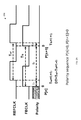
- FIG. 1 illustrates one embodiment of the invention showing an architecture of a fast frequency acquisition/control unit.
- FIG. 2A , FIG. 2B , FIG. 2C , and FIG. 2D illustrate various embodiments of the invention showing the timing measurement principle used.
- FIG. 3 illustrates one embodiment of the invention showing an example timing of 3 consecutive frequency control word (FCW) updating.
- FCW frequency control word
- FIG. 4 illustrates one embodiment of the invention showing a flow chart.
- FIG. 5 illustrates one embodiment of the invention showing an example of a time to digital converter implementation.
- FIG. 6 illustrates one embodiment of the invention showing application in an analog PLL system.
- FIG. 7 illustrates one embodiment of the invention showing application in a narrow bandwidth digital PLL system.
- FIG. 8 illustrates, one embodiment of the invention showing a bank selection logic block.
- FIG. 9 illustrates an embodiment of a VCO in block diagram form.
- FIG. 10 illustrates an embodiment of a VCO showing a transfer function in graph form.
- FIG. 11 illustrates an embodiment of a VCO.
- FIG. 12 illustrates an embodiment of a VCO in flow chart form.
- FIG. 13 illustrates one embodiment of a DCO (digitally controlled oscillator).
- FIG. 14 illustrates one embodiment of a DLPF (digital low pass filter).
- FIG. 15 illustrates one embodiment of a FSM (finite state machine).
- FIG. 16 illustrates one embodiment of a binary search or successive approximation.
- FIG. 17 illustrates embodiments of the invention showing an example of operation timing.
- FIG. 18 illustrates embodiments of the invention showing an example of a PFD implementation and operation timing.
- FIG. 19 illustrates an embodiment of the invention showing an example of start/stop logic.
- FIG. 20 illustrates embodiments of the invention showing an example of a Arbit logic implementation and operation timing.
- FIG. 21 illustrates an embodiment of the invention showing an example of a cycle slip detector.
- FIG. 22 illustrates an embodiment of the invention showing an example of a FSM (finite state machine).
- FSM finite state machine
- FIG. 23 illustrates, one embodiment of the invention showing a bank selection logic block.
- FIG. 24 illustrates, one embodiment of the invention showing a VCO band selection.
- a TDC Time to Digital Converter
- a time to digital converter tdc also denoted as TDC, includes logic for determining the time between a received start signal and a received stop signal. In one embodiment a tdc generates an output signal to indicate the time between a received start signal and a received stop signal.
- a binary search (sometimes called Successive Approximation) technique based method is used to achieve fast frequency acquisition in a narrow bandwidth PLL system.
- the invention can be applied to frequency calibration and feedback divider ratio control with improved convergence speed.
- a TDC and binary search technique is used to achieve fast frequency acquisition in a narrow bandwidth PLL system. It also can be applied to frequency calibration and feedback divider ratio control with improved convergence speed.
- cycle slip detection is applied to determine if a feedback clock from a DCO (Digitally Controlled Oscillator) or a VCO (Voltage Controlled Oscillator) is faster than a reference clock or not in one measurement cycle.
- DCO Digitally Controlled Oscillator
- VCO Voltage Controlled Oscillator
- a TDC is used to measure the phase difference between the feedback clock and a reference clock and a criterion is applied to determine if the clock is fast or slow.
- a binary search technique is directly applied for the digital frequency control word (FCW—frequency control word) to approximate the target frequency.
- FCW digital frequency control word
- the technique disclosed will converge as long as there is a monotonic function between the digital frequency control word and the VCO or DCO output frequency.
- the TDC resolution and accuracy is a guarantee of correct operation.
- cycle slip detection is used to determine a condition of fast or slow between a reference clock and the feedback clock.
- a TDC and a related truth table is used to determine fast or slow between the reference clock and the feedback clock.
- a binary search or successive approximation technique is applied to achieve fast convergence.
- fast acquisition and lock is a feature for a PLL utilizing the techniques disclosed.
- Fast Frequency Calibration/Acquisition/Search in a Frequency/Phase Lock Loop system is achieved utilizing the techniques disclosed.
- FIG. 1 illustrates, generally at 100 , one embodiment of the invention showing an architecture of a fast frequency acquisition/control unit.
- REFCLK reference clock signal
- FBCLK feedback clock signal
- PFD phase frequency detector
- UP up signal
- DN down signal
- TDC block 150 time to digital converter block
- the TDC block 150 has several sub-blocks which includes at 112 arbitration logic (Arbit logic), at 114 start/stop logic (Start/Stop logic), and at 124 a time to digital converter (tdc).
- Functional block 111 receives signals REFCLK 102 , FBCLK 104 , and UP 108 and DN 110 signals generated by PFD 106 as well as clear 154 and f_update 156 which originate from FSM 132 .
- 116 cycle slip detection logic Cycle slip detection
- dn_csd down signal
- up_csd up signal
- arbitration logic Aribit logic
- start/stop logic Start/Stop logic
- Functional unit 111 generates as output signals up_csd 128 and dn_csd 126 coming from Cycle slip detection 116 , P 160 coming form tdc 124 , Dph 158 coming from tdc 124 , done 152 coming from the Start/Stop logic 114 .
- FSM (finite state machine) 132 receives as input signals up_csd 128 and dn_csd 126 coming from Cycle slip detection 116 , P 160 coming from tdc 124 , Dph 158 coming from tdc 124 , and done 152 coming from the Start/Stop logic 114 .
- FSM 132 generates as output signals FCW (Frequency Control Word) 134 , a clear signal (clear) 154 , and a frequency update signal (f_update) 156 .
- FCW Frequency Control Word
- FIG. 1 is the architecture of a fast frequency acquisition/control unit. It has a PFD 106 , a Cycle slip detection block 116 , a tdc 124 and Start/Stop logic 114 and Arbit logic 112 , and a FSM 132 .
- a PFD detects the frequency/phase error information between two input clock signals and generates two signals.
- PFD 106 detects the frequency/phase error information between two input clock signals, i.e. REFCLK 102 and FBCLK 104 , and generates UP and DN signals ( 108 and 110 respectively) corresponding to REFCLK 102 and FBCLK's 104 transition (e.g. rising edge in this case), respectively.
- Start/Stop logic 114 generates control signals (start 122 and stop 120 ) for tdc 124 to quantize the UP/DN pulse difference coming from the UP 108 and DN 110 signals of PFD 106 , and Arbit logic 112 decides which edge comes first for one cycle operation (i.e. a measurement cycle). This allows the tdc 124 to quantize the UP/DN 108 / 110 pulse difference. In this approach, two consecutive phase differences are measured by TDC 150 and stored.
- a FSM 132 (which includes successive approximation logic) will estimate the instant period difference or frequency difference based on the digitized phase information and adjust the digital frequency control variables, such as, but not limited to, a voltage potential in a PLL loop filter capacitor, a VCO coarse tuning word, a LC-VCO (LC-tank based VCO) band calibration, a DCO frequency control word (FCW), a feedback divider ratio, etc.
- the digital frequency control word is updated every two REFCLK 102 or FBCLK 104 cycles, and FBCLK 104 frequency can be adjusted to close (i.e. frequency) with REFCLK 102 quickly within accuracy of tens of picoseconds resolution via using the TDC 150 .
- the PFD 106 experiences cycle slips whenever one or more clock transitions (either REFCLK 102 or FBCLK 104 ) occurs between 2 consecutive PFD reset operations (which are controlled by signal clear 154 ).
- the cycle slip indicator signals up_csd 128 and dn_csd 126 directly contains period information related to the PFD 106 input clocks 102 REFCLK and 104 FBCLK, and can be used to control frequency tuning.
- phase or period difference between REFCLK 102 and FBCLK 104 can be measured with the TDC 150 .
- FIG. 2A , FIG. 2B , FIG. 2C , and FIG. 2D illustrate, generally at 200 , 220 , 240 , and 260 respectively embodiments of the invention showing the timing measurement principle used and Table 1 below shows the corresponding FSM (e.g. FIG. 1 at 132 ) decision logic.
- the instant period difference (DT) can be calculated with two consecutive phase measurements using TDC 150 . It is easy to find out if the instant period difference DT is larger than 0 or not, i.e., the FBCLK 104 is faster than the REFCLK 102 when DT is larger than 0 and the FBCLK 104 is slower than the REFCLK 102 when DT is less than 0. Then the FSM will generate an internal signal INC/DECb to show the status and a binary search (sometimes called successive approximation) technique is implemented within the FSM to generate the FCW (frequency control word) to control the frequency of FBCLK 104 . We call these two consecutive phase measurements as one period difference measurement. The frequency control word (FCW) 134 will update once every period difference measurement. This update is indicated by signal f_update 156 .
- FCW frequency control word
- the Arbit logic 112 output Polarity signal 118
- the Start/Stop logic 114 output signals start 122 and stop 120 will have some meta-stability at edge transition, so a threshold Tthres (corresponding to ppm of target period) is applied for DT decision making. If abs(DT) (the absolute value of DT) is larger than the threshold Tthres, it means there is quite a large period difference or frequency difference between FBCLK (e.g. FIG. 1 at 104 ) and REFCLK (e.g. FIG. 1 at 102 ).
- abs(DT) is less than the threshold Tthres, it means FBCLK (e.g. FIG. 1 at 104 ) and REFCLK (e.g. FIG. 1 at 102 ) are close enough, and the FSM (e.g. FIG. 1 at 132 ) will stop the frequency binary search process and enter the next stage process, for example, phase acquisition.
- FBCLK e.g. FIG. 1 at 104
- REFCLK e.g. FIG. 1 at 102
- FIG. 3 illustrates, generally at 300 , one embodiment of the invention showing an example timing of 3 consecutive frequency control word (FCW) updating
- FIG. 4 illustrates, generally at 400 , one embodiment of the invention showing the FSM 132 flow chart processes every frequency control word updating.
- the frequency control word is reset to be FCW 0 and FBCLK is running at an initial clock rate.
- a DN_CSD event indicates FBCLK is higher than REFCLK, and the frequency control word changes to FCW 1 .
- a UP_CSD indicates FBCLK frequency is lower than REFCLK, and the frequency control word changes to FCW 2 .
- the 3rd period difference measurement cycle there is no cycle slip shown so the next frequency control word update will be based on FIGS. 2A, 2B, 2C, and 2D , and a Table 1 decision.
- the process starts at 402 Start.
- the PFD is reset.
- a first TDC measurement at 408 there is a first TDC measurement at 408 and a second TDC measurement at 410 and a cycle slip detection at 406 .
- a determination is made if up_csd 1 412 and if so then proceed to adjust the FCW (frequency control word, for example of a DCO (digitally controlled oscillator) to change its frequency) based on a binary search technique at 420 . If the determination is made that up_csd#1 412 then proceed to 414 .
- FCW frequency control word, for example of a DCO (digitally controlled oscillator)
- a determination is made if dn_csd 1 and if so then proceed to adjust the DCO FCW based on a binary search technique at 420 . If the determination is made that dn_csd#1 414 then proceed to 416 . At 416 calculate DT based on the TDC phase difference and polarity then proceed to 418 where a determination is made if
- FIG. 5 illustrates, generally at 500 , one embodiment of the invention showing an example of a tdc implementation (for example, most of tdc 124 in FIG. 1 ).
- Ring oscillator RingOsc 502 generates high speed multi-phase clocks P 1 , P 2 , . . . , P 32 (as indicated at 510 ).
- the counter (Counter) 514 When a “start” signal (start) 512 is logic high, the counter (Counter) 514 will calculate coarse phase by counting the number of “P 32 ” pulses 516 , when “stop” signal (stop) 518 is logic high, the latch (Latch & encoder) 520 will lock the RingOsc 502 clock phase status and encode it to be a fine phase (5 bit) 528 , at the same time, the counter 524 value 522 (14 bit) will be held as coarse.
- the coarse 522 , fine phase 528 , and polarity (Polarity and P) 524 are synchronized by system clock FSMCLK 526 and combined to provide the FSM 132 complete phase information (Dph) 530 .
- a TDC resolution of 100 ps can be easily implemented in a modern CMOS process, and the TDC can achieve a timing accuracy of 1000 ppm with only 2 consecutive TDC measurements for a 1 MHz reference clock. If we assume a 12-bit frequency control word is used to control a DCO, this approach will achieve an accuracy of 1/(2 ⁇ 12) or 250 ppm within 12 ⁇ 2 REFCLK cycles using this method.
- the invention is not so limited and a larger frequency control word may be used.
- this frequency control unit disclosed can be used to tune all frequency related objects with a significant convergence time improvement, for example, but not limited to a VCO coarse tune, a LC-VCO bank selection, a loop capacitor voltage potential preset, a feedback divider ratio preset, etc, as shown for example in FIG. 6 . More specifically the techniques disclosed can be used to speed-up the frequency acquisition in a very narrow bandwidth (for example, 1 Hz or lower) frequency/phase locked loop, as shown for example in FIG. 7 with a digital PLL implementation.
- a very narrow bandwidth for example, 1 Hz or lower
- FIG. 7 with a digital PLL implementation.
- some of the hardware for example, the PFD, tdc, could be shared or re-used from the loop. For illustration purposes we have, in some cases, duplicated what could be shared or re-used.
- FIG. 6 illustrates, generally at 600 , one embodiment of the invention showing application in an analog PLL system.
- 602 is the FreqCtrlUnit (frequency control unit) which outputs a FCW signal 618 that can be used for the LC-VCO bank select BSEL at 604 (showing 24 banks as an example (B 0 . . . B 23 )), the voltage control signal DVC at 606 going to the DAC (digital to analog converter) 616 , and the feedback divider N signal at 608 going to the FBDIV 612 (feedback divider circuit), at 610 is a PFD (phase frequency detector).
- the FreqCtrlUnit frequency control unit
- the PFD 610 determines the phase/frequency difference between the input signals REFCLK 620 and FBCLK 622 and generates output signals ph_up 624 and ph_dn 626 to indicate such.
- a charge pump At 628 is shown a charge pump.
- a charge pump generates an output current based on one or more inputs.
- charge pump 628 is coupled to receive signals ph_up 624 and ph_dn 626 .
- charge pump 628 outputs a current signal 630 which is shown coupled to filtering network 642 .
- a filtering network takes an input signal and generates an output signal that is different in some way from the input signal.
- the filtering network 642 includes a resistor 632 , a capacitor 634 , a capacitor 636 , a resistor 638 , and a capacitor 640 .
- a LC-VCO with banks is a voltage controlled oscillator having a series of inductors and capacitors arranged in banks where each bank can be selected and has a different inductor-capacitance value. Alternatively each selected bank may be considered to have a different impedance.
- LC-VCO with banks 614 is indicated to have 24 banks of inductor-capacitance values denoted as B 0 , B 1 , B 2 , . . . , B 21 , B 22 , B 23 the selection of which is controlled by a bank select signal.
- LC-VCO with banks 614 has a bank select input BSEL 604 which is coupled to receive a bank select signal.
- the bank select signal goes to a bank selection logic block which will select the inductor-capacitor for a given bank.
- An LC-VCO with banks will generate an output signal based upon an input voltage signal and a bank select signal.
- LC-VCO with banks 614 is coupled to receive input signal 644 which is an output signal from filtering network 642 , is coupled to receive a bank select signal 604 from the output signal FSW 618 of FreqCtrlUnit 602 , and generates an output signal VCOCLK 648 .
- a feedback divider is a circuit that takes in a signal and generates an output which is a fractional representation of the input signal.
- FBDIV (feedback divider) 612 is coupled to receive as input VCOCLK 648 and generate an output signal FBCLK 622 .
- a feedback divider has an additional input which can determine the fractional.
- FBDIV 612 has an input N 608 for receiving a signal to indicate the fractional. That fractional signal is received from the output signal FSW 618 of FreqCtrlUnit 602 .
- a frequency control unit generates signals to control the frequency of another signal.
- the frequency control unit FreqCtrlUnit 602 generates signals FCW 618 to control the frequency of signal VCOCLK 648 .
- FCW 618 goes to BSEL 604 which selects an inductor-capacitor bank which affects the frequency of VCOCLK 648
- FCW 618 also goes to N 608 which affects the frequency of VCOCLK 648
- FCW 618 goes to DVC 606 which controls the output signal voltage 646 of DAC 616 .
- the signal voltage 646 is received by the filtering network 642 and affects the network filtering 642 output signal 644 which is the voltage which also affects the frequency of the voltage controlled oscillator in the LC-VCO with banks 614 which outputs the frequency signal VCOCLK 648 .
- FreqCtrlUnit 602 receives additional input signals REFCLK 620 and FBCLK 622 .
- FreqCtrlUnit 602 may be, but is not limited to, an embodiment as illustrated in FIG. 1 .
- FIG. 7 illustrates, generally at 700 , one embodiment of the invention showing application in a narrow bandwidth digital PLL system.
- 702 is the FreqCtrlUnit (frequency control unit) which outputs a FCW signal 718 that can be used for controlling the DCO (digitally controlled oscillator) 714 via DW (digital word) 704 , and the feedback divider N at 708 .
- the feedback divider N signal at 708 going to the FBDIV 712 (feedback divider circuit), at 710 is a PFD (phase frequency detector).
- the PFD 710 determines the phase/frequency difference between the input signals REFCLK 720 and FBCLK 722 and generates output signals ph_up 724 and ph_dn 726 to indicate such.
- a TDC time to digital converter
- a time to digital converter converts a time into a digital representation.
- TDC 728 is coupled to receive signals ph_up 724 and ph_dn 726 .
- TDC 728 outputs a digital signal 730 which is shown coupled to a DLPF (digital low pass filter) 742 .
- a digital low pass filter takes an input signal and generates an output signal that has some of the high frequency components removed.
- the DLPF 742 receives an input signal 730 and generates an output signal 744 which goes to the DCO (digitally controlled oscillator) 714 .
- a DCO is an oscillator whose output frequency is controlled digitally. As such depending upon what digital input is received the DCO generates an output frequency.
- the DCO 714 generates an output signal DCOCLK (digitally controlled oscillator clock) 748 .
- DCO 714 receives 744 a digital signal from the DLPF 742 and DW 704 from FCW 718 .
- a feedback divider is a circuit that takes in a signal and generates an output which is a fractional representation of the input signal.
- FBDIV (feedback divider) 712 is coupled to receive as input DCOCLK 748 and generate an output signal FBCLK 722 .
- a feedback divider has an additional input which can determine the fractional.
- FBDIV 712 has an input N 708 for receiving a signal to indicate the fractional. That fractional signal is received from the output signal FSW 718 of FreqCtrlUnit 702 .
- a frequency control unit generates signals to control the frequency of another signal.
- the frequency control unit FreqCtrlUnit 702 generates signals FCW 718 to control the frequency of signal DCOCLK 748 .
- FCW 718 goes to DW 704 which affects the frequency of DCOCLK 748
- FCW 718 also goes to N 708 which affects the frequency of DCOCLK 748 .
- the FreqCtrlUnit 702 receives additional input signals REFCLK 720 and FBCLK 722 .
- FreqCtrlUnit 702 may be, but is not limited to, an embodiment as illustrated in FIG. 1 .
- FIG. 8 illustrates, generally at 800 , one embodiment of the invention showing a bank selection logic block.
- BSEL 802 receives the bank select signal, which in this embodiment is shown as D 0 , D 1 , D 2 , D 3 , and D 4 ( 802 - 0 , 802 - 1 , 802 - 2 , 802 - 3 , 802 - 4 respectively) which each respectively goes to a transistor T 0 , T 1 , T 2 , T 3 , and T 4 ( 804 - 0 , 804 - 1 , 804 - 2 , 804 - 3 , 802 - 4 respectively) for switching on/off said transistor and selecting or not selecting inductors L 1 , L 2 , L 3 , and L 4 ( 806 - 0 , 806 - 1 , 806 - 2 , 806 - 3 , 806 - 4 respectively).
- Inductor 808 and capacitor 810 form an LC network across which BSEL 802 controls additional inductances L 1 , L 2 , L 3 , and L 4 which can be in parallel with inductor 808 .
- Nodes 812 , 814 , and 816 would connect to the LC oscillator circuit and BSEL 802 now can select the banks of inductors for frequency control.
- a bank selection logic block For example, similar to FIG.
- an alternative embodiment might have the component at 810 being an inductor, with the components at 808 , and 804 - 0 , 804 - 1 , 804 - 2 , 804 - 3 , 802 - 4 being capacitors.
- One such embodiment is illustrated in FIG. 23 .
- a voltage controlled oscillator is a non-transitory hardware based device that takes as an input a transitory input voltage signal and generates a transitory oscillating output voltage signal whose frequency is based on the transitory input voltage signal.
- FIG. 9 illustrates, generally at 900 , an embodiment of a VCO in block diagram form.
- a transitory input voltage signal which goes into the VCO non-transitory hardware based device 904 , which then generates a transitory oscillating output signal 906 whose frequency is based on the transitory input voltage signal 902 .
- FIG. 10 illustrates, generally at 1000 , an embodiment of a VCO 1004 showing a transfer function 1008 in graph form.
- At 1002 is the transitory input voltage signal voltage level
- at 1006 is the transitory oscillating output signal frequency.
- 1001 indicates an increasing transitory voltage
- 205 indicates an increasing transitory frequency.
- FIG. 11 illustrates, generally at 1100 , an embodiment of a VCO.
- Transitory power is supplied at 1102 and 1104 , for example, in the form of a positive and ground voltage respectively.
- At 1106 is a non-transitory hardware device that takes as input the transitory power 1102 and produces at 1108 a transitory signal in the form of a transitory constant current.
- At 1110 and 1112 are non-transitory devices in the form of inductors which take as input a transitory constant current 1108 and generate a transitory output current signal 1114 and 1116 respectively whose transitory current summation is equal to that of transitory constant current 1108 .
- At 1118 is a transitory input voltage signal which goes to non-transitory hardware devices 1120 and 1122 both of which are in the form of a varactor diode.
- At 1124 is a transitory oscillating output signal.
- At 1126 and 1128 are non-transitory transistors that take as inputs the transitory output current signal 1114 and 1116 respectively and generate a transitory signal in the form of a transitory constant current equal in summation to that of transitory constant current 1108 plus any input current from transitory input voltage signal 1118 and minus any current from the transitory oscillating output signal 1124 .
- VCO 1100 is a tuned LC cross-coupled oscillator whose output frequency is adjusted by a voltage adjusting the C.
- FIG. 12 illustrates, generally at 1200 , an embodiment of a VCO in flow chart form.
- 1202 is the transitory input voltage signal.
- 1204 a determination is made if the transitory input voltage signal has changed in voltage and if not then take No 1214 back to 1204 . If yes then take Yes 1206 to block 1208 where we adjust the transitory oscillating output signal frequency based on the transitory input voltage signal. Then we proceed via 1212 back to 1204 .
- the transitory oscillating output signal is shown at 1210 .
- a DCO digital controlled oscillator takes as input a digital frequency signal and generates an oscillating output signal based on the digital frequency signal.
- FIG. 13 illustrates, generally at 1300 , one embodiment of a DCO (digitally controlled oscillator).
- a ring oscillator has a first inverter 1308 followed by pairs of inverters, such as 1309 - 1 , 1309 - 2 , . . . , 1309 - m , the pairs acting as delay elements.
- the Freq Sel 1304 input is coupled to receive a digital frequency signal.
- the output of the 1 of n selector 1302 is Output 1306 . In operation the Output 1306 supplies an oscillating output signal (Oscillator Output) 1310 .
- a DCO uses a DAC to control the voltage to a VCO.
- a NCO number of harmonics
- PAC phase to amplitude converter.
- a DCO uses a digital input (often called a frequency control word) to control the frequency versus an analog voltage used by a VCO.
- a DLPF digital low pass filter
- FIG. 14 illustrates, generally at 1400 , one embodiment of a DLPF (digital low pass filter).
- DLPF digital low pass filter
- At 1402 is a Digital Input which is coupled to receive a digital input signal.
- At 1412 is a Digital Output which is coupled to send a digital output signal.
- At 1404 and 1408 are summation units, and at 1406 and 1410 are Time Delay units.
- a summation unit takes signals from two inputs and generates a summation signal of the two input signals.
- a Time Delay unit receives as input an input signal and generates an output signal after a fixed amount of time (called the delay) that is the same as the received input signal.
- a FSM finite state machine
- a FSM has a fixed number of states (e.g. finite) and can be expressed visually in a state transition diagram which shows states, transitions from states, input signals, and output signals.
- FIG. 15 illustrates, generally at 1500 , one embodiment of a FSM (finite state machine).
- FSM finite state machine
- At 1502 is an input coupled to receive input signals.
- At 1504 is an output which generates signals.
- States are S 1 , S 2 , S 3 , S 4 , S 5 , . . . , Sk ( 1506 - 1 , 1506 - 2 , 1506 - 3 , 1506 - 4 , 1506 - 5 , 1506 - k respectively where k is a finite integer number.
- the interconnection of states and transitions and inputs and outputs is determined by the particular application.
- a binary search or successive approximation is a device (e.g. FSM (finite state machine)) that takes an input signal and via a search determines the value of the input signal.
- FSM finite state machine
- FIG. 16 illustrates, generally at 1600 , one embodiment of a binary search or successive approximation device implemented as a FSM showing in flow chart form the binary search.
- the Input signal and Output signal can be compared and the Output signal is in whatever form is needed for comparison.
- At 1602 we start by receiving the Input and clearing all bit in the Output word which controls the Output.
- At 1606 we compare the output to the input and if they are equal we are Done 1608 and know the value of the Input from the bits as set in the Output word.
- FIG. 17 illustrates, generally at 1700 and 1750 , embodiments of the invention showing an example of operation timing.
- REFCLK initially leading FBCLK At 1700 is shown REFCLK initially leading FBCLK.
- REFCLK initially lagging FBCLK At 1750 is shown REFCLK initially lagging FBCLK. If the initial phase difference between REFCLK and FBCLK changes in each frequency measurement cycle, even if the frequency of REFCLK and FBCLK are not changed, it may generate a different polarity value from the circuit. This is an exceptional case and is not fatal and is illustrated in FIG. 17 at 1700 and 1750 .
- FIG. 18 illustrates, generally at 1800 and 1850 , embodiments of the invention showing an example of a PFD implementation and operation timing ( 1800 and 1850 respectively).
- the PFD 1800 detects frequency/phase error information between two input clocks, i.e. REFCLK 1802 and FBCLK 1804 , and generates UP/DN pulse ( 1806 / 1808 respectively) corresponding to REFCLK 1802 and FBCLK's 1804 transition (rising edge in this case), respectively.
- a “clear” 1810 (clear) high pulse will reset the PFD 1800 output status.
- FIG. 19 illustrates, generally at 1900 , an embodiment of the invention showing an example of start/stop logic (Start/Stop logic).
- the start/stop logic generates various signals (start 1908 , stop 1912 , done 1916 ) to control the tdc (for example tdc 124 in FIG. 1 ).
- a “done” signal 1916 is delayed (via 1914 delay) of “stop” (stop) 1912 signal indicates the tdc has finished one UP/DN ( 1902 / 1904 ) phase measurement.
- 1906 is an OR gate
- 1910 is an AND gate.
- FIG. 20 illustrates, generally at 2000 and 2050 , embodiments of the invention showing an example of a Arbit logic implementation and operation timing ( 2000 and 2050 respectively).
- the polarity info (Polarity) 2002 is sent out at the rising edge of DN 2004 pulse generated by a PFD, and a “clear” pulse (clear) 2006 will reset the polarity info.
- DN 2004 pulse generated by a PFD
- clear “clear” pulse
- At 2006 is an UP signal and at 2008 is a flip-flop.
- FIG. 21 illustrates, generally at 2100 , an embodiment of the invention showing an example of a cycle slip detector (Cycle slip detection).
- At 2102 is an OR gate.
- At 2104 is a D-type flip-flop.
- At 2106 is a D-type flip-flop.
- At 2108 is an OR gate.
- At 2110 is a D-type flip-flop.
- At 2112 is a D-type flip-flop.
- At 2120 is a done signal.
- At 2122 is a clear signal.
- At 2124 is an UP signal.
- At 2126 is an f_update signal.
- At 2128 is a DN (down) signal.
- At 2134 is a REFCLK signal.
- At 2136 is a FBCLK signal.
- At 2140 is an up-csd signal.
- At 2142 is a dn_csd signal.
- FIG. 22 illustrates, generally at 2200 , an embodiment of the invention showing an example of a FSM (finite state machine).
- FSM finite state machine
- At 2230 is FSM which receives input signals FSMCLK 2202 , done 2204 , up_csd 2206 , dn_csd 2208 , Dph 2210 , and P 2212 , and which generates output signals clear 2222 , f_update 2224 , and FCW 2226 .
- the FSM will detect the signal “done” (done) 2204 all the time. When it detects that “done” (done) 2204 is logic high, it will sync all the input data from the TDC and start measurement cycles. It will generate a “clear” (clear) 2222 pulse every TDC phase measurement cycle, and an “_” (f_update) 2224 signal every two TDC phase measurement cycles, or every frequency measurement cycle.
- the frequency control word FCW 2226 will be updated every two TDC phase measurement cycles based on a binary search (or sometimes called successive approximation) technique.
- FIG. 22 illustrates an embodiment in block level format of the transitory signals input and output to the apparatus FSM 2230 .
- the FSM 2230 apparatus might utilize the FSM as shown in FIG. 15 to implement in hardware the functions shown in FIG. 4 combined with Table 1.
- FIG. 23 illustrates, generally at 23 , one embodiment of the invention showing a bank selection logic block.
- BSEL 2380 receives the bank select signal, which in this embodiment is shown as D 0 , D 1 , D 2 , and D 3 ( 2310 , 2311 , 2312 , 2313 respectively) which each respectively goes to transistors denoted 2340 , 2350 , 2360 , and 2370 for switching on/off said transistor and selecting or not selecting pairs of capacitors respectively denoted 2342 and 2344 , 2352 and 2354 , 2362 and 2364 , 2372 and 2374 to be active/inactive in the circuit.
- Inductor 2320 and capacitors 2322 and 2324 form an LC network across which BSEL 802 controls additional capacitances which can be in parallel with capacitors 2322 and 2324 .
- Nodes 2302 and 2304 would connect to the LC oscillator circuit and BSEL 2380 now can select the banks of capacitors for frequency control.
- BSEL 802 controls additional capacitances which can be in parallel with capacitors 2322 and 2324 .
- Nodes 2302 and 2304 would connect to the LC oscillator circuit and BSEL 2380 now can select the banks of capacitors for frequency control.
- FIG. 24 illustrates, generally at 2400 , one embodiment of the invention showing a VCO band selection.
- Transitory power is supplied at 2402 and 2404 , for example, in the form of a positive and ground voltage respectively.
- At 2406 is a non-transitory hardware device that takes as input the transitory power 2402 and produces at 2408 a transitory signal in the form of a transitory constant current.
- At 2410 and 2412 are non-transitory devices in the form of inductors which take as input a transitory constant current 2408 and generate a transitory output current signal 2414 and 2416 respectively whose transitory current summation is equal to that of transitory constant current 2408 .
- At 2418 is a transitory input voltage signal which goes to non-transitory hardware devices 2420 and 2422 both of which are in the form of a varactor diode.
- At 2424 is a transitory oscillating output signal.
- At 2426 and 2428 are non-transitory transistors that take as inputs the transitory output current signal 2414 and 2416 respectively and generate a transitory signal in the form of a transitory constant current equal in summation to that of transitory constant current 2408 plus any input current from transitory input voltage signal 2418 and minus any current from the transitory oscillating output signal 2424 .
- VCO 2400 is a tuned LC cross-coupled oscillator whose output frequency is adjusted by a voltage adjusting the C.
- Dashed box 2429 illustrates VCO band selection logic.
- D 0 , D 1 , D 2 , and D 3 2430 , 2431 , 2432 , and 2433 respectively
- respective capacitors pairs 2442 and 2444 , 2452 and 2454 , 2462 and 2464 , 2472 and 2474 may be controlled by respective transistors 2440 , 2450 , 2460 , and 2460 to add additional capacitance between nodes 2414 and 2416 thereby affecting the VCO LC network.
- embodiments of the present invention require specialized hardware.
- FSM finite state machine
- CPU central processing unit
- one embodiment or “an embodiment” or similar phrases means that the feature(s) being described are included in at least one embodiment of the invention. References to “one embodiment” in this description do not necessarily refer to the same embodiment; however, neither are such embodiments mutually exclusive. Nor does “one embodiment” imply that there is but a single embodiment of the invention. For example, a feature, structure, act, etc. described in “one embodiment” may also be included in other embodiments. Thus, the invention may include a variety of combinations and/or integrations of the embodiments described herein.
Landscapes
- Physics & Mathematics (AREA)
- General Physics & Mathematics (AREA)
- Stabilization Of Oscillater, Synchronisation, Frequency Synthesizers (AREA)
Abstract
Description
| TABLE 1 |
| Table 1. Decision table |
| input | output |
| P[n] | P[n + 1] | Abs(DT) > Tthres? | STAY/EXITb | Freq INC/ |
| 0 | 0 | 1 | 1 | 0 |
| 0 | 0 | x | ||
| 0 | 1 | 1 | 1 | 1 |
| 0 | 0 | x | ||
| 1 | 0 | 1 | 1 | 0 |
| 0 | 0 | x | ||
| 1 | 1 | 1 | 1 | 1 |
| 0 | 0 | x | ||
Claims (20)
Priority Applications (1)
| Application Number | Priority Date | Filing Date | Title |
|---|---|---|---|
| US14/794,770 US9362924B1 (en) | 2015-07-08 | 2015-07-08 | Method and apparatus for fast frequency acquisition in PLL system |
Applications Claiming Priority (1)
| Application Number | Priority Date | Filing Date | Title |
|---|---|---|---|
| US14/794,770 US9362924B1 (en) | 2015-07-08 | 2015-07-08 | Method and apparatus for fast frequency acquisition in PLL system |
Publications (1)
| Publication Number | Publication Date |
|---|---|
| US9362924B1 true US9362924B1 (en) | 2016-06-07 |
Family
ID=56083269
Family Applications (1)
| Application Number | Title | Priority Date | Filing Date |
|---|---|---|---|
| US14/794,770 Active US9362924B1 (en) | 2015-07-08 | 2015-07-08 | Method and apparatus for fast frequency acquisition in PLL system |
Country Status (1)
| Country | Link |
|---|---|
| US (1) | US9362924B1 (en) |
Cited By (7)
| Publication number | Priority date | Publication date | Assignee | Title |
|---|---|---|---|---|
| CN111600601A (en) * | 2019-02-20 | 2020-08-28 | 艾迪悌科技有限公司 | Feedback control for accurate signal generation |
| CN112710897A (en) * | 2020-12-07 | 2021-04-27 | 广东电网有限责任公司韶关供电局 | Frequency measuring circuit |
| US20220200608A1 (en) * | 2020-12-17 | 2022-06-23 | Qualcomm Incorporated | Digital phase-frequency detector with split control loops for low jitter and fast locking |
| US11588489B1 (en) | 2021-10-06 | 2023-02-21 | Shaoxing Yuanfang Semiconductor Co., Ltd. | Obtaining lock in a phase-locked loop (PLL) upon being out of phase-lock |
| US20230188144A1 (en) * | 2021-12-09 | 2023-06-15 | Lx Semicon Co., Ltd. | Clock recovery circuit for display |
| US11923864B2 (en) | 2021-10-18 | 2024-03-05 | Shaoxing Yuanfang Semiconductor Co., Ltd. | Fast switching of output frequency of a phase locked loop (PLL) |
| US11967965B2 (en) | 2021-11-03 | 2024-04-23 | Shaoxing Yuanfang Semiconductor Co., Ltd. | Generating divided signals from phase-locked loop (PLL) output when reference clock is unavailable |
Citations (4)
| Publication number | Priority date | Publication date | Assignee | Title |
|---|---|---|---|---|
| US20130211758A1 (en) * | 2012-02-15 | 2013-08-15 | Texas Instruments Incorporated | Reference clock re-timing scheme in electronic circuits |
| US8704564B2 (en) * | 2012-04-16 | 2014-04-22 | Fujitsu Semiconductor Limited | PLL circuit |
| US20140210532A1 (en) * | 2013-01-29 | 2014-07-31 | Perceptia Devices Australia Pty Ltd. | Phase-Locked Loop Apparatus and Method |
| US20140347941A1 (en) * | 2013-05-24 | 2014-11-27 | Qualcomm Incorporated | Low latency synchronization scheme for mesochronous ddr system |
-
2015
- 2015-07-08 US US14/794,770 patent/US9362924B1/en active Active
Patent Citations (4)
| Publication number | Priority date | Publication date | Assignee | Title |
|---|---|---|---|---|
| US20130211758A1 (en) * | 2012-02-15 | 2013-08-15 | Texas Instruments Incorporated | Reference clock re-timing scheme in electronic circuits |
| US8704564B2 (en) * | 2012-04-16 | 2014-04-22 | Fujitsu Semiconductor Limited | PLL circuit |
| US20140210532A1 (en) * | 2013-01-29 | 2014-07-31 | Perceptia Devices Australia Pty Ltd. | Phase-Locked Loop Apparatus and Method |
| US20140347941A1 (en) * | 2013-05-24 | 2014-11-27 | Qualcomm Incorporated | Low latency synchronization scheme for mesochronous ddr system |
Non-Patent Citations (4)
| Title |
|---|
| In-Chul Hwang et al. "A Digitally Controlled Phase-Locked Loop With a Digital Phase-Frequency Detector for Fast Acquisition," IEEE Journal of Solid-State Circuits, vol. 36, No. 10, Oct. 2001, pp. 1574-1581. |
| Mozhgan Mansuri et al. "Fast Frequency Acquisition Phase-Frequency Detectors for GSamples/s Phase-Locked Loops," IEEE Journal of Solid-State Circuits, vol. 37, No. 10, Oct. 2002, pp. 1331-1334. |
| Takamoto Watanabe and Shigenori Yamauchi "An All-Digital PLL for Frequency Multiplication by 4 to 1022 With Seven-Cycle Lock Time," IEEE Journal of Solid-State Circuits, vol. 38, No. 2, Feb. 2003, pp. 198-204. |
| V. Kratyuk et al. "Frequency detector for fast frequency lock of digital PLLs," Electronics Letters Jan. 4, 2007 vol. 43 No. 1, pp. |
Cited By (9)
| Publication number | Priority date | Publication date | Assignee | Title |
|---|---|---|---|---|
| CN111600601A (en) * | 2019-02-20 | 2020-08-28 | 艾迪悌科技有限公司 | Feedback control for accurate signal generation |
| CN112710897A (en) * | 2020-12-07 | 2021-04-27 | 广东电网有限责任公司韶关供电局 | Frequency measuring circuit |
| US20220200608A1 (en) * | 2020-12-17 | 2022-06-23 | Qualcomm Incorporated | Digital phase-frequency detector with split control loops for low jitter and fast locking |
| US11533058B2 (en) * | 2020-12-17 | 2022-12-20 | Qualcomm Incorporated | Digital phase-frequency detector with split control loops for low jitter and fast locking |
| US11588489B1 (en) | 2021-10-06 | 2023-02-21 | Shaoxing Yuanfang Semiconductor Co., Ltd. | Obtaining lock in a phase-locked loop (PLL) upon being out of phase-lock |
| US11923864B2 (en) | 2021-10-18 | 2024-03-05 | Shaoxing Yuanfang Semiconductor Co., Ltd. | Fast switching of output frequency of a phase locked loop (PLL) |
| US11967965B2 (en) | 2021-11-03 | 2024-04-23 | Shaoxing Yuanfang Semiconductor Co., Ltd. | Generating divided signals from phase-locked loop (PLL) output when reference clock is unavailable |
| US20230188144A1 (en) * | 2021-12-09 | 2023-06-15 | Lx Semicon Co., Ltd. | Clock recovery circuit for display |
| US11791826B2 (en) * | 2021-12-09 | 2023-10-17 | Lx Semicon Co., Ltd. | Clock recovery circuit for display |
Similar Documents
| Publication | Publication Date | Title |
|---|---|---|
| US9362924B1 (en) | Method and apparatus for fast frequency acquisition in PLL system | |
| US9838024B2 (en) | Auto frequency calibration method | |
| KR101632657B1 (en) | Time-to-digital convertoer and all-digital phase locked loop | |
| US8957712B2 (en) | Mixed signal TDC with embedded T2V ADC | |
| US7746182B2 (en) | Systems and methods for voltage controlled oscillator calibration | |
| US8804892B2 (en) | Frequency and phase acquisition of a clock and data recovery circuit without an external reference clock | |
| JP5590867B2 (en) | Time / digital converter and digital phase lock loop | |
| US8102197B1 (en) | Digital phase locked loop | |
| KR101231743B1 (en) | Digital lock detector and frequency synthesizer using the same | |
| US9998128B2 (en) | Frequency synthesizer with injection locked oscillator | |
| US20110074514A1 (en) | Frequency measurement circuit and pll synthesizer provided therewith | |
| JP5347534B2 (en) | Phase comparator, PLL circuit, and phase comparator control method | |
| US7804925B2 (en) | Detection arrangement, counter unit, phase locked loop, detection method and method for generating an oscillator signal | |
| US8947139B1 (en) | Apparatus for doubling the dynamic range of a time to digital converter | |
| US7592874B2 (en) | Phase/frequency detector, phase locked loop, method for phase/frequency detection and method for generating an oscillator signal | |
| US7724093B2 (en) | Phase locked loop with two-step control | |
| EP2797235B1 (en) | Phase-locked loop device with managed transition to random noise operation mode | |
| US10018970B2 (en) | Time-to-digital system and associated frequency synthesizer | |
| EP2502349A1 (en) | A phase locked loop | |
| US7869555B2 (en) | Digital word representative of a non-integer ratio between the respective periods of two signals | |
| JP2007142791A (en) | Frequency synthesizer | |
| US20190068204A1 (en) | Frequency locking circuitry and clock data recovery circuitry | |
| Huang et al. | A time-to-digital converter based AFC for wideband frequency synthesizer | |
| KR101716411B1 (en) | Oscillating circuit, PLL circuit, and signal processing device | |
| JP5310135B2 (en) | Digital PLL circuit |
Legal Events
| Date | Code | Title | Description |
|---|---|---|---|
| AS | Assignment |
Owner name: INTEGRATED DEVICE TECHNOLOGY, INC., CALIFORNIA Free format text: ASSIGNMENT OF ASSIGNORS INTEREST;ASSIGNORS:XU, CHANGXI;LI, HUI;REEL/FRAME:036036/0315 Effective date: 20150706 |
|
| STCF | Information on status: patent grant |
Free format text: PATENTED CASE |
|
| CC | Certificate of correction | ||
| AS | Assignment |
Owner name: JPMORGAN CHASE BANK, N.A., AS COLLATERAL AGENT, NE Free format text: SECURITY AGREEMENT;ASSIGNORS:INTEGRATED DEVICE TECHNOLOGY, INC.;GIGPEAK, INC.;MAGNUM SEMICONDUCTOR, INC.;AND OTHERS;REEL/FRAME:042166/0431 Effective date: 20170404 Owner name: JPMORGAN CHASE BANK, N.A., AS COLLATERAL AGENT, NEW YORK Free format text: SECURITY AGREEMENT;ASSIGNORS:INTEGRATED DEVICE TECHNOLOGY, INC.;GIGPEAK, INC.;MAGNUM SEMICONDUCTOR, INC.;AND OTHERS;REEL/FRAME:042166/0431 Effective date: 20170404 |
|
| AS | Assignment |
Owner name: INTEGRATED DEVICE TECHNOLOGY, INC., CALIFORNIA Free format text: RELEASE BY SECURED PARTY;ASSIGNOR:JPMORGAN CHASE BANK, N.A.;REEL/FRAME:048746/0001 Effective date: 20190329 Owner name: CHIPX, INCORPORATED, CALIFORNIA Free format text: RELEASE BY SECURED PARTY;ASSIGNOR:JPMORGAN CHASE BANK, N.A.;REEL/FRAME:048746/0001 Effective date: 20190329 Owner name: ENDWAVE CORPORATION, CALIFORNIA Free format text: RELEASE BY SECURED PARTY;ASSIGNOR:JPMORGAN CHASE BANK, N.A.;REEL/FRAME:048746/0001 Effective date: 20190329 Owner name: MAGNUM SEMICONDUCTOR, INC., CALIFORNIA Free format text: RELEASE BY SECURED PARTY;ASSIGNOR:JPMORGAN CHASE BANK, N.A.;REEL/FRAME:048746/0001 Effective date: 20190329 Owner name: GIGPEAK, INC., CALIFORNIA Free format text: RELEASE BY SECURED PARTY;ASSIGNOR:JPMORGAN CHASE BANK, N.A.;REEL/FRAME:048746/0001 Effective date: 20190329 |
|
| MAFP | Maintenance fee payment |
Free format text: PAYMENT OF MAINTENANCE FEE, 4TH YEAR, LARGE ENTITY (ORIGINAL EVENT CODE: M1551); ENTITY STATUS OF PATENT OWNER: LARGE ENTITY Year of fee payment: 4 |
|
| MAFP | Maintenance fee payment |
Free format text: PAYMENT OF MAINTENANCE FEE, 8TH YEAR, LARGE ENTITY (ORIGINAL EVENT CODE: M1552); ENTITY STATUS OF PATENT OWNER: LARGE ENTITY Year of fee payment: 8 |