EP3023970A2 - Anzeigetafel zur kompensation von negativer stromversorgungsspannung, anzeigemodul und mobile vorrichtung damit - Google Patents
Anzeigetafel zur kompensation von negativer stromversorgungsspannung, anzeigemodul und mobile vorrichtung damit Download PDFInfo
- Publication number
- EP3023970A2 EP3023970A2 EP15170750.2A EP15170750A EP3023970A2 EP 3023970 A2 EP3023970 A2 EP 3023970A2 EP 15170750 A EP15170750 A EP 15170750A EP 3023970 A2 EP3023970 A2 EP 3023970A2
- Authority
- EP
- European Patent Office
- Prior art keywords
- voltage lines
- negative voltage
- display panel
- cathode electrode
- compensation
- Prior art date
- Legal status (The legal status is an assumption and is not a legal conclusion. Google has not performed a legal analysis and makes no representation as to the accuracy of the status listed.)
- Withdrawn
Links
Images












Classifications
-
- G—PHYSICS
- G09—EDUCATION; CRYPTOGRAPHY; DISPLAY; ADVERTISING; SEALS
- G09G—ARRANGEMENTS OR CIRCUITS FOR CONTROL OF INDICATING DEVICES USING STATIC MEANS TO PRESENT VARIABLE INFORMATION
- G09G3/00—Control arrangements or circuits, of interest only in connection with visual indicators other than cathode-ray tubes
- G09G3/20—Control arrangements or circuits, of interest only in connection with visual indicators other than cathode-ray tubes for presentation of an assembly of a number of characters, e.g. a page, by composing the assembly by combination of individual elements arranged in a matrix no fixed position being assigned to or needed to be assigned to the individual characters or partial characters
- G09G3/22—Control arrangements or circuits, of interest only in connection with visual indicators other than cathode-ray tubes for presentation of an assembly of a number of characters, e.g. a page, by composing the assembly by combination of individual elements arranged in a matrix no fixed position being assigned to or needed to be assigned to the individual characters or partial characters using controlled light sources
- G09G3/30—Control arrangements or circuits, of interest only in connection with visual indicators other than cathode-ray tubes for presentation of an assembly of a number of characters, e.g. a page, by composing the assembly by combination of individual elements arranged in a matrix no fixed position being assigned to or needed to be assigned to the individual characters or partial characters using controlled light sources using electroluminescent panels
- G09G3/32—Control arrangements or circuits, of interest only in connection with visual indicators other than cathode-ray tubes for presentation of an assembly of a number of characters, e.g. a page, by composing the assembly by combination of individual elements arranged in a matrix no fixed position being assigned to or needed to be assigned to the individual characters or partial characters using controlled light sources using electroluminescent panels semiconductive, e.g. using light-emitting diodes [LED]
- G09G3/3208—Control arrangements or circuits, of interest only in connection with visual indicators other than cathode-ray tubes for presentation of an assembly of a number of characters, e.g. a page, by composing the assembly by combination of individual elements arranged in a matrix no fixed position being assigned to or needed to be assigned to the individual characters or partial characters using controlled light sources using electroluminescent panels semiconductive, e.g. using light-emitting diodes [LED] organic, e.g. using organic light-emitting diodes [OLED]
- G09G3/3225—Control arrangements or circuits, of interest only in connection with visual indicators other than cathode-ray tubes for presentation of an assembly of a number of characters, e.g. a page, by composing the assembly by combination of individual elements arranged in a matrix no fixed position being assigned to or needed to be assigned to the individual characters or partial characters using controlled light sources using electroluminescent panels semiconductive, e.g. using light-emitting diodes [LED] organic, e.g. using organic light-emitting diodes [OLED] using an active matrix
- G09G3/3233—Control arrangements or circuits, of interest only in connection with visual indicators other than cathode-ray tubes for presentation of an assembly of a number of characters, e.g. a page, by composing the assembly by combination of individual elements arranged in a matrix no fixed position being assigned to or needed to be assigned to the individual characters or partial characters using controlled light sources using electroluminescent panels semiconductive, e.g. using light-emitting diodes [LED] organic, e.g. using organic light-emitting diodes [OLED] using an active matrix with pixel circuitry controlling the current through the light-emitting element
-
- H—ELECTRICITY
- H10—SEMICONDUCTOR DEVICES; ELECTRIC SOLID-STATE DEVICES NOT OTHERWISE PROVIDED FOR
- H10K—ORGANIC ELECTRIC SOLID-STATE DEVICES
- H10K59/00—Integrated devices, or assemblies of multiple devices, comprising at least one organic light-emitting element covered by group H10K50/00
- H10K59/10—OLED displays
- H10K59/12—Active-matrix OLED [AMOLED] displays
- H10K59/131—Interconnections, e.g. wiring lines or terminals
-
- G—PHYSICS
- G09—EDUCATION; CRYPTOGRAPHY; DISPLAY; ADVERTISING; SEALS
- G09G—ARRANGEMENTS OR CIRCUITS FOR CONTROL OF INDICATING DEVICES USING STATIC MEANS TO PRESENT VARIABLE INFORMATION
- G09G3/00—Control arrangements or circuits, of interest only in connection with visual indicators other than cathode-ray tubes
- G09G3/20—Control arrangements or circuits, of interest only in connection with visual indicators other than cathode-ray tubes for presentation of an assembly of a number of characters, e.g. a page, by composing the assembly by combination of individual elements arranged in a matrix no fixed position being assigned to or needed to be assigned to the individual characters or partial characters
- G09G3/22—Control arrangements or circuits, of interest only in connection with visual indicators other than cathode-ray tubes for presentation of an assembly of a number of characters, e.g. a page, by composing the assembly by combination of individual elements arranged in a matrix no fixed position being assigned to or needed to be assigned to the individual characters or partial characters using controlled light sources
- G09G3/30—Control arrangements or circuits, of interest only in connection with visual indicators other than cathode-ray tubes for presentation of an assembly of a number of characters, e.g. a page, by composing the assembly by combination of individual elements arranged in a matrix no fixed position being assigned to or needed to be assigned to the individual characters or partial characters using controlled light sources using electroluminescent panels
- G09G3/32—Control arrangements or circuits, of interest only in connection with visual indicators other than cathode-ray tubes for presentation of an assembly of a number of characters, e.g. a page, by composing the assembly by combination of individual elements arranged in a matrix no fixed position being assigned to or needed to be assigned to the individual characters or partial characters using controlled light sources using electroluminescent panels semiconductive, e.g. using light-emitting diodes [LED]
- G09G3/3208—Control arrangements or circuits, of interest only in connection with visual indicators other than cathode-ray tubes for presentation of an assembly of a number of characters, e.g. a page, by composing the assembly by combination of individual elements arranged in a matrix no fixed position being assigned to or needed to be assigned to the individual characters or partial characters using controlled light sources using electroluminescent panels semiconductive, e.g. using light-emitting diodes [LED] organic, e.g. using organic light-emitting diodes [OLED]
- G09G3/3225—Control arrangements or circuits, of interest only in connection with visual indicators other than cathode-ray tubes for presentation of an assembly of a number of characters, e.g. a page, by composing the assembly by combination of individual elements arranged in a matrix no fixed position being assigned to or needed to be assigned to the individual characters or partial characters using controlled light sources using electroluminescent panels semiconductive, e.g. using light-emitting diodes [LED] organic, e.g. using organic light-emitting diodes [OLED] using an active matrix
-
- G—PHYSICS
- G09—EDUCATION; CRYPTOGRAPHY; DISPLAY; ADVERTISING; SEALS
- G09G—ARRANGEMENTS OR CIRCUITS FOR CONTROL OF INDICATING DEVICES USING STATIC MEANS TO PRESENT VARIABLE INFORMATION
- G09G3/00—Control arrangements or circuits, of interest only in connection with visual indicators other than cathode-ray tubes
- G09G3/20—Control arrangements or circuits, of interest only in connection with visual indicators other than cathode-ray tubes for presentation of an assembly of a number of characters, e.g. a page, by composing the assembly by combination of individual elements arranged in a matrix no fixed position being assigned to or needed to be assigned to the individual characters or partial characters
- G09G3/22—Control arrangements or circuits, of interest only in connection with visual indicators other than cathode-ray tubes for presentation of an assembly of a number of characters, e.g. a page, by composing the assembly by combination of individual elements arranged in a matrix no fixed position being assigned to or needed to be assigned to the individual characters or partial characters using controlled light sources
- G09G3/30—Control arrangements or circuits, of interest only in connection with visual indicators other than cathode-ray tubes for presentation of an assembly of a number of characters, e.g. a page, by composing the assembly by combination of individual elements arranged in a matrix no fixed position being assigned to or needed to be assigned to the individual characters or partial characters using controlled light sources using electroluminescent panels
- G09G3/32—Control arrangements or circuits, of interest only in connection with visual indicators other than cathode-ray tubes for presentation of an assembly of a number of characters, e.g. a page, by composing the assembly by combination of individual elements arranged in a matrix no fixed position being assigned to or needed to be assigned to the individual characters or partial characters using controlled light sources using electroluminescent panels semiconductive, e.g. using light-emitting diodes [LED]
- G09G3/3208—Control arrangements or circuits, of interest only in connection with visual indicators other than cathode-ray tubes for presentation of an assembly of a number of characters, e.g. a page, by composing the assembly by combination of individual elements arranged in a matrix no fixed position being assigned to or needed to be assigned to the individual characters or partial characters using controlled light sources using electroluminescent panels semiconductive, e.g. using light-emitting diodes [LED] organic, e.g. using organic light-emitting diodes [OLED]
- G09G3/3225—Control arrangements or circuits, of interest only in connection with visual indicators other than cathode-ray tubes for presentation of an assembly of a number of characters, e.g. a page, by composing the assembly by combination of individual elements arranged in a matrix no fixed position being assigned to or needed to be assigned to the individual characters or partial characters using controlled light sources using electroluminescent panels semiconductive, e.g. using light-emitting diodes [LED] organic, e.g. using organic light-emitting diodes [OLED] using an active matrix
- G09G3/3258—Control arrangements or circuits, of interest only in connection with visual indicators other than cathode-ray tubes for presentation of an assembly of a number of characters, e.g. a page, by composing the assembly by combination of individual elements arranged in a matrix no fixed position being assigned to or needed to be assigned to the individual characters or partial characters using controlled light sources using electroluminescent panels semiconductive, e.g. using light-emitting diodes [LED] organic, e.g. using organic light-emitting diodes [OLED] using an active matrix with pixel circuitry controlling the voltage across the light-emitting element
-
- G—PHYSICS
- G09—EDUCATION; CRYPTOGRAPHY; DISPLAY; ADVERTISING; SEALS
- G09G—ARRANGEMENTS OR CIRCUITS FOR CONTROL OF INDICATING DEVICES USING STATIC MEANS TO PRESENT VARIABLE INFORMATION
- G09G3/00—Control arrangements or circuits, of interest only in connection with visual indicators other than cathode-ray tubes
- G09G3/20—Control arrangements or circuits, of interest only in connection with visual indicators other than cathode-ray tubes for presentation of an assembly of a number of characters, e.g. a page, by composing the assembly by combination of individual elements arranged in a matrix no fixed position being assigned to or needed to be assigned to the individual characters or partial characters
- G09G3/22—Control arrangements or circuits, of interest only in connection with visual indicators other than cathode-ray tubes for presentation of an assembly of a number of characters, e.g. a page, by composing the assembly by combination of individual elements arranged in a matrix no fixed position being assigned to or needed to be assigned to the individual characters or partial characters using controlled light sources
- G09G3/30—Control arrangements or circuits, of interest only in connection with visual indicators other than cathode-ray tubes for presentation of an assembly of a number of characters, e.g. a page, by composing the assembly by combination of individual elements arranged in a matrix no fixed position being assigned to or needed to be assigned to the individual characters or partial characters using controlled light sources using electroluminescent panels
- G09G3/32—Control arrangements or circuits, of interest only in connection with visual indicators other than cathode-ray tubes for presentation of an assembly of a number of characters, e.g. a page, by composing the assembly by combination of individual elements arranged in a matrix no fixed position being assigned to or needed to be assigned to the individual characters or partial characters using controlled light sources using electroluminescent panels semiconductive, e.g. using light-emitting diodes [LED]
- G09G3/3208—Control arrangements or circuits, of interest only in connection with visual indicators other than cathode-ray tubes for presentation of an assembly of a number of characters, e.g. a page, by composing the assembly by combination of individual elements arranged in a matrix no fixed position being assigned to or needed to be assigned to the individual characters or partial characters using controlled light sources using electroluminescent panels semiconductive, e.g. using light-emitting diodes [LED] organic, e.g. using organic light-emitting diodes [OLED]
- G09G3/3266—Details of drivers for scan electrodes
-
- G—PHYSICS
- G09—EDUCATION; CRYPTOGRAPHY; DISPLAY; ADVERTISING; SEALS
- G09G—ARRANGEMENTS OR CIRCUITS FOR CONTROL OF INDICATING DEVICES USING STATIC MEANS TO PRESENT VARIABLE INFORMATION
- G09G3/00—Control arrangements or circuits, of interest only in connection with visual indicators other than cathode-ray tubes
- G09G3/20—Control arrangements or circuits, of interest only in connection with visual indicators other than cathode-ray tubes for presentation of an assembly of a number of characters, e.g. a page, by composing the assembly by combination of individual elements arranged in a matrix no fixed position being assigned to or needed to be assigned to the individual characters or partial characters
- G09G3/22—Control arrangements or circuits, of interest only in connection with visual indicators other than cathode-ray tubes for presentation of an assembly of a number of characters, e.g. a page, by composing the assembly by combination of individual elements arranged in a matrix no fixed position being assigned to or needed to be assigned to the individual characters or partial characters using controlled light sources
- G09G3/30—Control arrangements or circuits, of interest only in connection with visual indicators other than cathode-ray tubes for presentation of an assembly of a number of characters, e.g. a page, by composing the assembly by combination of individual elements arranged in a matrix no fixed position being assigned to or needed to be assigned to the individual characters or partial characters using controlled light sources using electroluminescent panels
- G09G3/32—Control arrangements or circuits, of interest only in connection with visual indicators other than cathode-ray tubes for presentation of an assembly of a number of characters, e.g. a page, by composing the assembly by combination of individual elements arranged in a matrix no fixed position being assigned to or needed to be assigned to the individual characters or partial characters using controlled light sources using electroluminescent panels semiconductive, e.g. using light-emitting diodes [LED]
- G09G3/3208—Control arrangements or circuits, of interest only in connection with visual indicators other than cathode-ray tubes for presentation of an assembly of a number of characters, e.g. a page, by composing the assembly by combination of individual elements arranged in a matrix no fixed position being assigned to or needed to be assigned to the individual characters or partial characters using controlled light sources using electroluminescent panels semiconductive, e.g. using light-emitting diodes [LED] organic, e.g. using organic light-emitting diodes [OLED]
- G09G3/3275—Details of drivers for data electrodes
-
- H—ELECTRICITY
- H10—SEMICONDUCTOR DEVICES; ELECTRIC SOLID-STATE DEVICES NOT OTHERWISE PROVIDED FOR
- H10D—INORGANIC ELECTRIC SEMICONDUCTOR DEVICES
- H10D86/00—Integrated devices formed in or on insulating or conducting substrates, e.g. formed in silicon-on-insulator [SOI] substrates or on stainless steel or glass substrates
- H10D86/01—Manufacture or treatment
- H10D86/021—Manufacture or treatment of multiple TFTs
-
- H—ELECTRICITY
- H10—SEMICONDUCTOR DEVICES; ELECTRIC SOLID-STATE DEVICES NOT OTHERWISE PROVIDED FOR
- H10D—INORGANIC ELECTRIC SEMICONDUCTOR DEVICES
- H10D86/00—Integrated devices formed in or on insulating or conducting substrates, e.g. formed in silicon-on-insulator [SOI] substrates or on stainless steel or glass substrates
- H10D86/40—Integrated devices formed in or on insulating or conducting substrates, e.g. formed in silicon-on-insulator [SOI] substrates or on stainless steel or glass substrates characterised by multiple TFTs
- H10D86/441—Interconnections, e.g. scanning lines
-
- H—ELECTRICITY
- H10—SEMICONDUCTOR DEVICES; ELECTRIC SOLID-STATE DEVICES NOT OTHERWISE PROVIDED FOR
- H10D—INORGANIC ELECTRIC SEMICONDUCTOR DEVICES
- H10D86/00—Integrated devices formed in or on insulating or conducting substrates, e.g. formed in silicon-on-insulator [SOI] substrates or on stainless steel or glass substrates
- H10D86/40—Integrated devices formed in or on insulating or conducting substrates, e.g. formed in silicon-on-insulator [SOI] substrates or on stainless steel or glass substrates characterised by multiple TFTs
- H10D86/60—Integrated devices formed in or on insulating or conducting substrates, e.g. formed in silicon-on-insulator [SOI] substrates or on stainless steel or glass substrates characterised by multiple TFTs wherein the TFTs are in active matrices
-
- H—ELECTRICITY
- H10—SEMICONDUCTOR DEVICES; ELECTRIC SOLID-STATE DEVICES NOT OTHERWISE PROVIDED FOR
- H10H—INORGANIC LIGHT-EMITTING SEMICONDUCTOR DEVICES HAVING POTENTIAL BARRIERS
- H10H20/00—Individual inorganic light-emitting semiconductor devices having potential barriers, e.g. light-emitting diodes [LED]
- H10H20/80—Constructional details
- H10H20/83—Electrodes
- H10H20/831—Electrodes characterised by their shape
-
- H—ELECTRICITY
- H10—SEMICONDUCTOR DEVICES; ELECTRIC SOLID-STATE DEVICES NOT OTHERWISE PROVIDED FOR
- H10H—INORGANIC LIGHT-EMITTING SEMICONDUCTOR DEVICES HAVING POTENTIAL BARRIERS
- H10H29/00—Integrated devices, or assemblies of multiple devices, comprising at least one light-emitting semiconductor element covered by group H10H20/00
- H10H29/10—Integrated devices comprising at least one light-emitting semiconductor component covered by group H10H20/00
- H10H29/14—Integrated devices comprising at least one light-emitting semiconductor component covered by group H10H20/00 comprising multiple light-emitting semiconductor components
- H10H29/142—Two-dimensional arrangements, e.g. asymmetric LED layout
-
- H—ELECTRICITY
- H10—SEMICONDUCTOR DEVICES; ELECTRIC SOLID-STATE DEVICES NOT OTHERWISE PROVIDED FOR
- H10K—ORGANIC ELECTRIC SOLID-STATE DEVICES
- H10K50/00—Organic light-emitting devices
- H10K50/80—Constructional details
- H10K50/805—Electrodes
- H10K50/82—Cathodes
- H10K50/822—Cathodes characterised by their shape
-
- H—ELECTRICITY
- H10—SEMICONDUCTOR DEVICES; ELECTRIC SOLID-STATE DEVICES NOT OTHERWISE PROVIDED FOR
- H10K—ORGANIC ELECTRIC SOLID-STATE DEVICES
- H10K59/00—Integrated devices, or assemblies of multiple devices, comprising at least one organic light-emitting element covered by group H10K50/00
- H10K59/10—OLED displays
- H10K59/12—Active-matrix OLED [AMOLED] displays
- H10K59/131—Interconnections, e.g. wiring lines or terminals
- H10K59/1315—Interconnections, e.g. wiring lines or terminals comprising structures specially adapted for lowering the resistance
-
- H—ELECTRICITY
- H10—SEMICONDUCTOR DEVICES; ELECTRIC SOLID-STATE DEVICES NOT OTHERWISE PROVIDED FOR
- H10K—ORGANIC ELECTRIC SOLID-STATE DEVICES
- H10K59/00—Integrated devices, or assemblies of multiple devices, comprising at least one organic light-emitting element covered by group H10K50/00
- H10K59/80—Constructional details
- H10K59/805—Electrodes
- H10K59/8052—Cathodes
- H10K59/80522—Cathodes combined with auxiliary electrodes
-
- G—PHYSICS
- G09—EDUCATION; CRYPTOGRAPHY; DISPLAY; ADVERTISING; SEALS
- G09G—ARRANGEMENTS OR CIRCUITS FOR CONTROL OF INDICATING DEVICES USING STATIC MEANS TO PRESENT VARIABLE INFORMATION
- G09G2300/00—Aspects of the constitution of display devices
- G09G2300/04—Structural and physical details of display devices
- G09G2300/0421—Structural details of the set of electrodes
- G09G2300/0426—Layout of electrodes and connections
-
- G—PHYSICS
- G09—EDUCATION; CRYPTOGRAPHY; DISPLAY; ADVERTISING; SEALS
- G09G—ARRANGEMENTS OR CIRCUITS FOR CONTROL OF INDICATING DEVICES USING STATIC MEANS TO PRESENT VARIABLE INFORMATION
- G09G2300/00—Aspects of the constitution of display devices
- G09G2300/04—Structural and physical details of display devices
- G09G2300/0421—Structural details of the set of electrodes
- G09G2300/043—Compensation electrodes or other additional electrodes in matrix displays related to distortions or compensation signals, e.g. for modifying TFT threshold voltage in column driver
-
- G—PHYSICS
- G09—EDUCATION; CRYPTOGRAPHY; DISPLAY; ADVERTISING; SEALS
- G09G—ARRANGEMENTS OR CIRCUITS FOR CONTROL OF INDICATING DEVICES USING STATIC MEANS TO PRESENT VARIABLE INFORMATION
- G09G2300/00—Aspects of the constitution of display devices
- G09G2300/04—Structural and physical details of display devices
- G09G2300/0439—Pixel structures
- G09G2300/0452—Details of colour pixel setup, e.g. pixel composed of a red, a blue and two green components
-
- G—PHYSICS
- G09—EDUCATION; CRYPTOGRAPHY; DISPLAY; ADVERTISING; SEALS
- G09G—ARRANGEMENTS OR CIRCUITS FOR CONTROL OF INDICATING DEVICES USING STATIC MEANS TO PRESENT VARIABLE INFORMATION
- G09G2300/00—Aspects of the constitution of display devices
- G09G2300/04—Structural and physical details of display devices
- G09G2300/0439—Pixel structures
- G09G2300/0465—Improved aperture ratio, e.g. by size reduction of the pixel circuit, e.g. for improving the pixel density or the maximum displayable luminance or brightness
-
- G—PHYSICS
- G09—EDUCATION; CRYPTOGRAPHY; DISPLAY; ADVERTISING; SEALS
- G09G—ARRANGEMENTS OR CIRCUITS FOR CONTROL OF INDICATING DEVICES USING STATIC MEANS TO PRESENT VARIABLE INFORMATION
- G09G2300/00—Aspects of the constitution of display devices
- G09G2300/08—Active matrix structure, i.e. with use of active elements, inclusive of non-linear two terminal elements, in the pixels together with light emitting or modulating elements
- G09G2300/0809—Several active elements per pixel in active matrix panels
-
- G—PHYSICS
- G09—EDUCATION; CRYPTOGRAPHY; DISPLAY; ADVERTISING; SEALS
- G09G—ARRANGEMENTS OR CIRCUITS FOR CONTROL OF INDICATING DEVICES USING STATIC MEANS TO PRESENT VARIABLE INFORMATION
- G09G2300/00—Aspects of the constitution of display devices
- G09G2300/08—Active matrix structure, i.e. with use of active elements, inclusive of non-linear two terminal elements, in the pixels together with light emitting or modulating elements
- G09G2300/0809—Several active elements per pixel in active matrix panels
- G09G2300/0819—Several active elements per pixel in active matrix panels used for counteracting undesired variations, e.g. feedback or autozeroing
-
- G—PHYSICS
- G09—EDUCATION; CRYPTOGRAPHY; DISPLAY; ADVERTISING; SEALS
- G09G—ARRANGEMENTS OR CIRCUITS FOR CONTROL OF INDICATING DEVICES USING STATIC MEANS TO PRESENT VARIABLE INFORMATION
- G09G2300/00—Aspects of the constitution of display devices
- G09G2300/08—Active matrix structure, i.e. with use of active elements, inclusive of non-linear two terminal elements, in the pixels together with light emitting or modulating elements
- G09G2300/0809—Several active elements per pixel in active matrix panels
- G09G2300/0842—Several active elements per pixel in active matrix panels forming a memory circuit, e.g. a dynamic memory with one capacitor
- G09G2300/0861—Several active elements per pixel in active matrix panels forming a memory circuit, e.g. a dynamic memory with one capacitor with additional control of the display period without amending the charge stored in a pixel memory, e.g. by means of additional select electrodes
-
- G—PHYSICS
- G09—EDUCATION; CRYPTOGRAPHY; DISPLAY; ADVERTISING; SEALS
- G09G—ARRANGEMENTS OR CIRCUITS FOR CONTROL OF INDICATING DEVICES USING STATIC MEANS TO PRESENT VARIABLE INFORMATION
- G09G2310/00—Command of the display device
- G09G2310/02—Addressing, scanning or driving the display screen or processing steps related thereto
- G09G2310/0243—Details of the generation of driving signals
- G09G2310/0251—Precharge or discharge of pixel before applying new pixel voltage
-
- G—PHYSICS
- G09—EDUCATION; CRYPTOGRAPHY; DISPLAY; ADVERTISING; SEALS
- G09G—ARRANGEMENTS OR CIRCUITS FOR CONTROL OF INDICATING DEVICES USING STATIC MEANS TO PRESENT VARIABLE INFORMATION
- G09G2310/00—Command of the display device
- G09G2310/08—Details of timing specific for flat panels, other than clock recovery
-
- G—PHYSICS
- G09—EDUCATION; CRYPTOGRAPHY; DISPLAY; ADVERTISING; SEALS
- G09G—ARRANGEMENTS OR CIRCUITS FOR CONTROL OF INDICATING DEVICES USING STATIC MEANS TO PRESENT VARIABLE INFORMATION
- G09G2320/00—Control of display operating conditions
- G09G2320/02—Improving the quality of display appearance
- G09G2320/0223—Compensation for problems related to R-C delay and attenuation in electrodes of matrix panels, e.g. in gate electrodes or on-substrate video signal electrodes
-
- G—PHYSICS
- G09—EDUCATION; CRYPTOGRAPHY; DISPLAY; ADVERTISING; SEALS
- G09G—ARRANGEMENTS OR CIRCUITS FOR CONTROL OF INDICATING DEVICES USING STATIC MEANS TO PRESENT VARIABLE INFORMATION
- G09G2320/00—Control of display operating conditions
- G09G2320/02—Improving the quality of display appearance
- G09G2320/0233—Improving the luminance or brightness uniformity across the screen
-
- G—PHYSICS
- G09—EDUCATION; CRYPTOGRAPHY; DISPLAY; ADVERTISING; SEALS
- G09G—ARRANGEMENTS OR CIRCUITS FOR CONTROL OF INDICATING DEVICES USING STATIC MEANS TO PRESENT VARIABLE INFORMATION
- G09G2330/00—Aspects of power supply; Aspects of display protection and defect management
- G09G2330/02—Details of power systems and of start or stop of display operation
- G09G2330/021—Power management, e.g. power saving
-
- H—ELECTRICITY
- H10—SEMICONDUCTOR DEVICES; ELECTRIC SOLID-STATE DEVICES NOT OTHERWISE PROVIDED FOR
- H10K—ORGANIC ELECTRIC SOLID-STATE DEVICES
- H10K50/00—Organic light-emitting devices
- H10K50/80—Constructional details
- H10K50/805—Electrodes
- H10K50/82—Cathodes
- H10K50/824—Cathodes combined with auxiliary electrodes
-
- H—ELECTRICITY
- H10—SEMICONDUCTOR DEVICES; ELECTRIC SOLID-STATE DEVICES NOT OTHERWISE PROVIDED FOR
- H10K—ORGANIC ELECTRIC SOLID-STATE DEVICES
- H10K59/00—Integrated devices, or assemblies of multiple devices, comprising at least one organic light-emitting element covered by group H10K50/00
- H10K59/10—OLED displays
- H10K59/12—Active-matrix OLED [AMOLED] displays
- H10K59/1201—Manufacture or treatment
Definitions
- electroluminescent displays can be driven with quick response speed and reduced power consumption, using a light-emitting diode (LED) or an organic light-emitting diode (OLED) that emits light through the recombination of electrons and holes.
- the luminance of an electroluminescent display device is determined (or controlled) by a global driving current that is the sum of respective pixel driving currents. In other words, the higher global driving current is supplied (e.g., required) when the displayed image has a higher brightness.
- At least one aspect of an embodiment of the present invention provides a display device capable of compensating a negative power supply voltage.
- the display panel may further include a plurality of positive voltage lines and a plurality of initialization voltage lines.
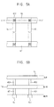
- the positive voltage lines may be formed in a first metal layer and may be configured to provide a positive power supply voltage to the pixel units, and the positive voltage lines may extend along the column direction and be arranged along the row direction.
- the display panel may further include a plurality initialization voltage lines formed in the first metal layer and configured to provide an initialization voltage to the pixel units.
- the initialization voltage lines may extend along the column direction and may be arranged along the row direction.
- the compensation negative voltage lines may be formed in the first metal layer through the same manufacturing processes as the manufacturing processes of the positive voltage lines and the initialization voltage lines.
- the compensation negative voltage lines may be formed in an anode layer over the first metal layer through a manufacturing processes different from manufacturing processes of the positive voltage lines and the initialization voltage lines, where anode electrodes of light-emitting diodes in the pixel units are formed in the anode layer.
- the ring-shaped edge negative voltage line and the compensation negative voltage lines may be formed in a same metal layer.
- the ring-shaped edge negative voltage line and the compensation negative voltage lines may be patterned through the same manufacturing processes and may be directly connected to each other.
- the ring-shaped edge negative voltage line and the compensation negative voltage lines may be connected to each other through a plurality of vertical contacts.
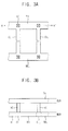
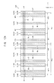
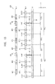
- the display panel 300 may include a substrate 301, a buffer layer 305, an active pattern 310, a gate insulation layer 330, a sixth gate electrode 335, a first insulation interlayer 340, connection patterns 351 and 352 formed in the metal layer 350, a second insulation interlayer 355, an anode electrode 360, a pixel definition layer 365, an organic light-emitting layer 370, and a cathode electrode 375.
- the system on chip 802 may control a power state and an operation state of a camcorder through a camcorder interface 813, control a power state and an operation state of a TV module through a TV interface 814, and control a power state and an operation state of a camera module or an image sensor module through an image sensor interface 815.
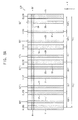
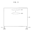
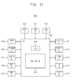
- the display module 1140 includes a display panel and the display panel includes a cathode electrode, a ring-shaped edge negative voltage line, and a plurality of compensation negative voltage lines.
- the cathode electrode is formed in a cathode region such that the cathode electrode may cover an entire active region in which a plurality of pixel units are formed.
- the ring-shaped edge negative voltage line is formed in a ring-shaped edge portion of the cathode electrode to drive a negative power supply voltage to the cathode electrode.
- the compensation negative voltage lines are connected to the ring-shaped edge negative voltage line.
- the compensation negative voltage lines are extended in a column direction and arranged (e.g., arranged repeatedly or spaced apart from one another) along a row direction.
Landscapes
- Engineering & Computer Science (AREA)
- Physics & Mathematics (AREA)
- Computer Hardware Design (AREA)
- General Physics & Mathematics (AREA)
- Theoretical Computer Science (AREA)
- Microelectronics & Electronic Packaging (AREA)
- Optics & Photonics (AREA)
- Electroluminescent Light Sources (AREA)
- Control Of El Displays (AREA)
- Devices For Indicating Variable Information By Combining Individual Elements (AREA)
- Control Of Indicators Other Than Cathode Ray Tubes (AREA)
- Manufacturing & Machinery (AREA)
Applications Claiming Priority (1)
| Application Number | Priority Date | Filing Date | Title |
|---|---|---|---|
| KR1020140147845A KR102272230B1 (ko) | 2014-10-29 | 2014-10-29 | 음의 전원 전압을 보상하기 위한 디스플레이 패널, 이를 포함하는 디스플레이 모듈 및 모바일 장치 |
Publications (2)
| Publication Number | Publication Date |
|---|---|
| EP3023970A2 true EP3023970A2 (de) | 2016-05-25 |
| EP3023970A3 EP3023970A3 (de) | 2016-08-24 |
Family
ID=53442489
Family Applications (1)
| Application Number | Title | Priority Date | Filing Date |
|---|---|---|---|
| EP15170750.2A Withdrawn EP3023970A3 (de) | 2014-10-29 | 2015-06-05 | Anzeigetafel zur kompensation von negativer stromversorgungsspannung, anzeigemodul und mobile vorrichtung damit |
Country Status (4)
| Country | Link |
|---|---|
| US (2) | US9373662B2 (de) |
| EP (1) | EP3023970A3 (de) |
| KR (4) | KR102272230B1 (de) |
| CN (2) | CN112785981B (de) |
Families Citing this family (17)
| Publication number | Priority date | Publication date | Assignee | Title |
|---|---|---|---|---|
| CN104103674B (zh) * | 2014-08-04 | 2017-04-12 | 石益坚 | 一种电容驱动电致发光显示器及其制造方法 |
| KR102272230B1 (ko) * | 2014-10-29 | 2021-07-05 | 삼성디스플레이 주식회사 | 음의 전원 전압을 보상하기 위한 디스플레이 패널, 이를 포함하는 디스플레이 모듈 및 모바일 장치 |
| JP2018522308A (ja) * | 2015-05-11 | 2018-08-09 | 華為技術有限公司Huawei Technologies Co.,Ltd. | タッチシステム、アクティブマトリクス型有機発光ダイオードパネル、及びディスプレイ駆動方法 |
| CN113192459A (zh) * | 2015-09-02 | 2021-07-30 | 天马微电子股份有限公司 | 显示装置 |
| KR102353726B1 (ko) | 2017-03-31 | 2022-01-20 | 삼성디스플레이 주식회사 | 표시 장치 |
| CN119942966A (zh) * | 2018-12-12 | 2025-05-06 | 群创光电股份有限公司 | 电子装置 |
| KR20210064483A (ko) | 2019-11-25 | 2021-06-03 | 삼성디스플레이 주식회사 | 입력 감지 기능을 갖는 표시 패널 및 표시 장치 |
| KR20210086309A (ko) * | 2019-12-31 | 2021-07-08 | 엘지디스플레이 주식회사 | 발광 표시 장치와 이를 이용한 멀티 스크린 표시 장치 |
| KR102734877B1 (ko) | 2020-03-10 | 2024-11-28 | 삼성디스플레이 주식회사 | 화소 회로 |
| KR102753463B1 (ko) * | 2020-04-21 | 2025-01-13 | 삼성디스플레이 주식회사 | 표시장치 |
| WO2021226804A1 (zh) * | 2020-05-11 | 2021-11-18 | 深圳市艾比森光电股份有限公司 | 一种负电压双电压电源驱动的led显示屏 |
| KR102814635B1 (ko) | 2020-05-28 | 2025-06-02 | 삼성디스플레이 주식회사 | 표시 장치 |
| KR102773247B1 (ko) | 2020-07-23 | 2025-02-28 | 삼성디스플레이 주식회사 | 화소 및 이를 포함하는 표시 장치 |
| CN112037716B (zh) * | 2020-09-21 | 2022-01-21 | 京东方科技集团股份有限公司 | 像素电路、显示面板和显示设备 |
| CN113450730B (zh) | 2021-07-26 | 2022-07-12 | 北京显芯科技有限公司 | 背光补偿方法、设备、系统及存储介质 |
| US12310196B2 (en) | 2022-05-31 | 2025-05-20 | Chengdu Boe Optoelectronics Technology Co., Ltd. | Display paneland display device |
| US12322337B2 (en) | 2022-05-31 | 2025-06-03 | Chengdu Boe Optoelectronics Technology Co., Ltd. | Display panel and display device |
Family Cites Families (22)
| Publication number | Priority date | Publication date | Assignee | Title |
|---|---|---|---|---|
| US7224118B2 (en) * | 2003-06-17 | 2007-05-29 | Semiconductor Energy Laboratory Co., Ltd. | Display device and electronic apparatus having a wiring connected to a counter electrode via an opening portion in an insulating layer that surrounds a pixel electrode |
| JP4121514B2 (ja) * | 2004-07-22 | 2008-07-23 | シャープ株式会社 | 有機発光素子、及び、それを備えた表示装置 |
| KR100635509B1 (ko) * | 2005-08-16 | 2006-10-17 | 삼성에스디아이 주식회사 | 유기 전계발광 표시장치 |
| JP5401784B2 (ja) * | 2007-02-08 | 2014-01-29 | セイコーエプソン株式会社 | 発光装置 |
| US7839083B2 (en) * | 2007-02-08 | 2010-11-23 | Seiko Epson Corporation | Light emitting device and electronic apparatus |
| KR101341788B1 (ko) * | 2007-07-09 | 2013-12-13 | 엘지디스플레이 주식회사 | 발광 표시장치 및 그의 구동방법 |
| JP5115180B2 (ja) * | 2007-12-21 | 2013-01-09 | ソニー株式会社 | 自発光型表示装置およびその駆動方法 |
| KR101286538B1 (ko) * | 2008-04-10 | 2013-07-16 | 엘지디스플레이 주식회사 | 액정 표시 장치 |
| KR101762344B1 (ko) * | 2010-07-27 | 2017-07-31 | 삼성디스플레이 주식회사 | 유기 전계 발광 표시 장치 |
| KR101450949B1 (ko) * | 2011-10-04 | 2014-10-16 | 엘지디스플레이 주식회사 | 유기발광 표시장치 |
| KR20130060934A (ko) | 2011-11-30 | 2013-06-10 | 삼성디스플레이 주식회사 | 유기 발광 표시 장치 및 그 제조방법 |
| JP5953923B2 (ja) * | 2012-05-15 | 2016-07-20 | セイコーエプソン株式会社 | 電気光学装置および電子機器 |
| JPWO2013171938A1 (ja) * | 2012-05-16 | 2016-01-07 | 株式会社Joled | 表示装置 |
| KR101928379B1 (ko) * | 2012-06-14 | 2018-12-12 | 엘지디스플레이 주식회사 | 유기발광 다이오드 표시장치 및 그 구동방법 |
| KR102011985B1 (ko) * | 2012-07-23 | 2019-08-20 | 삼성디스플레이 주식회사 | 표시 장치 및 그 구동 방법 |
| KR101486038B1 (ko) * | 2012-08-02 | 2015-01-26 | 삼성디스플레이 주식회사 | 유기 발광 표시 장치 |
| US8933453B2 (en) | 2012-08-29 | 2015-01-13 | Apple Inc. | Routing for high resolution and large size displays |
| KR20140029992A (ko) * | 2012-08-31 | 2014-03-11 | 삼성디스플레이 주식회사 | 박막 트랜지스터 어레이 기판, 이를 포함하는 표시 장치 |
| KR20140033834A (ko) | 2012-09-11 | 2014-03-19 | 삼성디스플레이 주식회사 | 전원 라인 배치 방법, 이를 채용하는 표시 패널 모듈 및 이를 구비하는 유기 발광 표시 장치 |
| KR101980763B1 (ko) * | 2012-12-21 | 2019-05-22 | 엘지디스플레이 주식회사 | 유기 발광 다이오드 표시장치와 그 구동방법 |
| CN103199096B (zh) * | 2013-04-18 | 2014-12-17 | 上海和辉光电有限公司 | 薄膜晶体管阵列基板及其制造方法 |
| KR102272230B1 (ko) * | 2014-10-29 | 2021-07-05 | 삼성디스플레이 주식회사 | 음의 전원 전압을 보상하기 위한 디스플레이 패널, 이를 포함하는 디스플레이 모듈 및 모바일 장치 |
-
2014
- 2014-10-29 KR KR1020140147845A patent/KR102272230B1/ko active Active
-
2015
- 2015-04-09 US US14/683,094 patent/US9373662B2/en active Active
- 2015-06-05 EP EP15170750.2A patent/EP3023970A3/de not_active Withdrawn
- 2015-06-15 CN CN202110061479.XA patent/CN112785981B/zh active Active
- 2015-06-15 CN CN201510328810.4A patent/CN106205446B/zh active Active
-
2016
- 2016-06-20 US US15/187,438 patent/US9704917B2/en active Active
-
2021
- 2021-06-25 KR KR1020210083452A patent/KR102394241B1/ko active Active
-
2022
- 2022-04-29 KR KR1020220053333A patent/KR102614899B1/ko active Active
-
2023
- 2023-12-12 KR KR1020230180184A patent/KR102856670B1/ko active Active
Non-Patent Citations (1)
| Title |
|---|
| None |
Also Published As
| Publication number | Publication date |
|---|---|
| CN112785981A (zh) | 2021-05-11 |
| CN106205446B (zh) | 2021-02-05 |
| KR102856670B1 (ko) | 2025-09-09 |
| KR20160052844A (ko) | 2016-05-13 |
| US20160293663A1 (en) | 2016-10-06 |
| KR102272230B1 (ko) | 2021-07-05 |
| KR102614899B1 (ko) | 2023-12-20 |
| KR102394241B1 (ko) | 2022-05-06 |
| KR20230171418A (ko) | 2023-12-20 |
| US9704917B2 (en) | 2017-07-11 |
| US20160126287A1 (en) | 2016-05-05 |
| CN112785981B (zh) | 2024-04-12 |
| US9373662B2 (en) | 2016-06-21 |
| CN106205446A (zh) | 2016-12-07 |
| EP3023970A3 (de) | 2016-08-24 |
| KR20210084376A (ko) | 2021-07-07 |
| KR20220061938A (ko) | 2022-05-13 |
Similar Documents
| Publication | Publication Date | Title |
|---|---|---|
| KR102856670B1 (ko) | 음의 전원 전압을 보상하기 위한 디스플레이 패널, 이를 포함하는 디스플레이 모듈 및 모바일 장치 | |
| CN110085646B (zh) | 有机发光显示面板和显示装置 | |
| CN109559679B (zh) | 触控显示面板及其驱动方法、像素电路、电子装置 | |
| US10297617B2 (en) | Display device and manufacturing method thereof | |
| CN108122500B (zh) | 晶体管基板、有机发光显示面板及有机发光显示装置 | |
| US9337247B2 (en) | Organic light-emitting diode display with bottom shields | |
| US9716134B2 (en) | Organic light-emitting diode display with bottom shields | |
| CN110992880A (zh) | 一种显示面板及显示装置 | |
| US10163393B2 (en) | Display substrate, display equipment and regional compensation method | |
| CN112309332A (zh) | 像素电路及其驱动方法、显示基板和显示面板 | |
| US11296169B2 (en) | Array substrate, display panel, and display device each having improved resolution | |
| WO2023226013A1 (zh) | 像素电路及其驱动方法、显示基板、显示装置 | |
| CN116917979A (zh) | 像素组、阵列基板和显示面板 | |
| CN118785747A (zh) | 显示基板以及显示装置 | |
| US20260004737A1 (en) | Display device and driving method thereof | |
| CN112365837A (zh) | 一种像素电路、其驱动方法及显示装置 | |
| KR102510401B1 (ko) | 표시 장치 및 그 제조 방법 | |
| US20250351645A1 (en) | Display device, electronic device and method of manufacturing display device | |
| KR20250156541A (ko) | 디스플레이 장치 | |
| CN118870866A (zh) | 显示装置 |
Legal Events
| Date | Code | Title | Description |
|---|---|---|---|
| AK | Designated contracting states |
Kind code of ref document: A2 Designated state(s): AL AT BE BG CH CY CZ DE DK EE ES FI FR GB GR HR HU IE IS IT LI LT LU LV MC MK MT NL NO PL PT RO RS SE SI SK SM TR |
|
| AX | Request for extension of the european patent |
Extension state: BA ME |
|
| PUAI | Public reference made under article 153(3) epc to a published international application that has entered the european phase |
Free format text: ORIGINAL CODE: 0009012 |
|
| PUAL | Search report despatched |
Free format text: ORIGINAL CODE: 0009013 |
|
| AK | Designated contracting states |
Kind code of ref document: A3 Designated state(s): AL AT BE BG CH CY CZ DE DK EE ES FI FR GB GR HR HU IE IS IT LI LT LU LV MC MK MT NL NO PL PT RO RS SE SI SK SM TR |
|
| AX | Request for extension of the european patent |
Extension state: BA ME |
|
| RIC1 | Information provided on ipc code assigned before grant |
Ipc: H01L 27/32 20060101ALI20160719BHEP Ipc: G09G 3/32 20060101ALI20160719BHEP Ipc: H01L 51/52 20060101ALI20160719BHEP Ipc: H01L 23/528 20060101ALI20160719BHEP Ipc: G09G 3/20 20060101AFI20160719BHEP |
|
| STAA | Information on the status of an ep patent application or granted ep patent |
Free format text: STATUS: REQUEST FOR EXAMINATION WAS MADE |
|
| 17P | Request for examination filed |
Effective date: 20170104 |
|
| RBV | Designated contracting states (corrected) |
Designated state(s): AL AT BE BG CH CY CZ DE DK EE ES FI FR GB GR HR HU IE IS IT LI LT LU LV MC MK MT NL NO PL PT RO RS SE SI SK SM TR |
|
| STAA | Information on the status of an ep patent application or granted ep patent |
Free format text: STATUS: EXAMINATION IS IN PROGRESS |
|
| 17Q | First examination report despatched |
Effective date: 20170517 |
|
| STAA | Information on the status of an ep patent application or granted ep patent |
Free format text: STATUS: THE APPLICATION IS DEEMED TO BE WITHDRAWN |
|
| 18D | Application deemed to be withdrawn |
Effective date: 20170728 |