EP3020035B1 - Anzeigevorrichtung - Google Patents
Anzeigevorrichtung Download PDFInfo
- Publication number
- EP3020035B1 EP3020035B1 EP13889182.5A EP13889182A EP3020035B1 EP 3020035 B1 EP3020035 B1 EP 3020035B1 EP 13889182 A EP13889182 A EP 13889182A EP 3020035 B1 EP3020035 B1 EP 3020035B1
- Authority
- EP
- European Patent Office
- Prior art keywords
- display device
- panel
- adhesive layer
- plate
- metal plate
- Prior art date
- Legal status (The legal status is an assumption and is not a legal conclusion. Google has not performed a legal analysis and makes no representation as to the accuracy of the status listed.)
- Active
Links
Images


Classifications
-
- G—PHYSICS
- G09—EDUCATION; CRYPTOGRAPHY; DISPLAY; ADVERTISING; SEALS
- G09F—DISPLAYING; ADVERTISING; SIGNS; LABELS OR NAME-PLATES; SEALS
- G09F9/00—Indicating arrangements for variable information in which the information is built-up on a support by selection or combination of individual elements
-
- H—ELECTRICITY
- H05—ELECTRIC TECHNIQUES NOT OTHERWISE PROVIDED FOR
- H05K—PRINTED CIRCUITS; CASINGS OR CONSTRUCTIONAL DETAILS OF ELECTRIC APPARATUS; MANUFACTURE OF ASSEMBLAGES OF ELECTRICAL COMPONENTS
- H05K7/00—Constructional details common to different types of electric apparatus
- H05K7/20—Modifications to facilitate cooling, ventilating, or heating
- H05K7/20954—Modifications to facilitate cooling, ventilating, or heating for display panels
- H05K7/20963—Heat transfer by conduction from internal heat source to heat radiating structure
-
- G—PHYSICS
- G06—COMPUTING OR CALCULATING; COUNTING
- G06F—ELECTRIC DIGITAL DATA PROCESSING
- G06F1/00—Details not covered by groups G06F3/00 - G06F13/00 and G06F21/00
- G06F1/16—Constructional details or arrangements
- G06F1/1601—Constructional details related to the housing of computer displays, e.g. of CRT monitors, of flat displays
-
- G—PHYSICS
- G06—COMPUTING OR CALCULATING; COUNTING
- G06F—ELECTRIC DIGITAL DATA PROCESSING
- G06F1/00—Details not covered by groups G06F3/00 - G06F13/00 and G06F21/00
- G06F1/16—Constructional details or arrangements
- G06F1/1613—Constructional details or arrangements for portable computers
- G06F1/1633—Constructional details or arrangements of portable computers not specific to the type of enclosures covered by groups G06F1/1615 - G06F1/1626
- G06F1/1637—Details related to the display arrangement, including those related to the mounting of the display in the housing
-
- G—PHYSICS
- G09—EDUCATION; CRYPTOGRAPHY; DISPLAY; ADVERTISING; SEALS
- G09F—DISPLAYING; ADVERTISING; SIGNS; LABELS OR NAME-PLATES; SEALS
- G09F9/00—Indicating arrangements for variable information in which the information is built-up on a support by selection or combination of individual elements
- G09F9/30—Indicating arrangements for variable information in which the information is built-up on a support by selection or combination of individual elements in which the desired character or characters are formed by combining individual elements
-
- H—ELECTRICITY
- H05—ELECTRIC TECHNIQUES NOT OTHERWISE PROVIDED FOR
- H05K—PRINTED CIRCUITS; CASINGS OR CONSTRUCTIONAL DETAILS OF ELECTRIC APPARATUS; MANUFACTURE OF ASSEMBLAGES OF ELECTRICAL COMPONENTS
- H05K5/00—Casings, cabinets or drawers for electric apparatus
- H05K5/0017—Casings, cabinets or drawers for electric apparatus with operator interface units
-
- H—ELECTRICITY
- H05—ELECTRIC TECHNIQUES NOT OTHERWISE PROVIDED FOR
- H05K—PRINTED CIRCUITS; CASINGS OR CONSTRUCTIONAL DETAILS OF ELECTRIC APPARATUS; MANUFACTURE OF ASSEMBLAGES OF ELECTRICAL COMPONENTS
- H05K5/00—Casings, cabinets or drawers for electric apparatus
- H05K5/02—Details
- H05K5/03—Covers
-
- H—ELECTRICITY
- H05—ELECTRIC TECHNIQUES NOT OTHERWISE PROVIDED FOR
- H05K—PRINTED CIRCUITS; CASINGS OR CONSTRUCTIONAL DETAILS OF ELECTRIC APPARATUS; MANUFACTURE OF ASSEMBLAGES OF ELECTRICAL COMPONENTS
- H05K5/00—Casings, cabinets or drawers for electric apparatus
- H05K5/10—Casings, cabinets or drawers for electric apparatus comprising several parts forming a closed casing
- H05K5/13—Casings, cabinets or drawers for electric apparatus comprising several parts forming a closed casing assembled by screws
-
- G—PHYSICS
- G02—OPTICS
- G02F—OPTICAL DEVICES OR ARRANGEMENTS FOR THE CONTROL OF LIGHT BY MODIFICATION OF THE OPTICAL PROPERTIES OF THE MEDIA OF THE ELEMENTS INVOLVED THEREIN; NON-LINEAR OPTICS; FREQUENCY-CHANGING OF LIGHT; OPTICAL LOGIC ELEMENTS; OPTICAL ANALOGUE/DIGITAL CONVERTERS
- G02F1/00—Devices or arrangements for the control of the intensity, colour, phase, polarisation or direction of light arriving from an independent light source, e.g. switching, gating or modulating; Non-linear optics
- G02F1/01—Devices or arrangements for the control of the intensity, colour, phase, polarisation or direction of light arriving from an independent light source, e.g. switching, gating or modulating; Non-linear optics for the control of the intensity, phase, polarisation or colour
- G02F1/13—Devices or arrangements for the control of the intensity, colour, phase, polarisation or direction of light arriving from an independent light source, e.g. switching, gating or modulating; Non-linear optics for the control of the intensity, phase, polarisation or colour based on liquid crystals, e.g. single liquid crystal display cells
- G02F1/133—Constructional arrangements; Operation of liquid crystal cells; Circuit arrangements
- G02F1/1333—Constructional arrangements; Manufacturing methods
- G02F1/133308—Support structures for LCD panels, e.g. frames or bezels
- G02F1/133314—Back frames
-
- G—PHYSICS
- G06—COMPUTING OR CALCULATING; COUNTING
- G06F—ELECTRIC DIGITAL DATA PROCESSING
- G06F2200/00—Indexing scheme relating to G06F1/04 - G06F1/32
- G06F2200/16—Indexing scheme relating to G06F1/16 - G06F1/18
- G06F2200/161—Indexing scheme relating to constructional details of the monitor
- G06F2200/1612—Flat panel monitor
Definitions
- the present disclosure relates to a display device that includes a multi-layered panel having a honeycomb pattern mesh.
- a conventional display device using a liquid crystal display panel or a plasma display panel includes a glass panel providing a basic screen, an intermediate frame, and a rear cover.
- the intermediate frame serves to support a variety of display device drive circuits arranged thereon, and to connect the glass panel and the rear cover to each other.
- the rear cover serves to increase rigidity of the entire display device, to efficiently radiate heat generated from the circuits, and to define an external appearance of the display device.
- a representative material for a typical rear cover of conventional display devices is a metal material, such as aluminum, this material may limit mechanical properties of the rear cover as the thickness of the rear cover is extremely reduced.
- the present invention is directed to a display device that substantially obviates one or more problems due to limitations and disadvantages of the related art.
- An object of the present invention is to provide a display device having a sandwich honeycomb panel to minimize bending deformation due to thermal expansion.
- a display device includes a display panel, a sandwich honeycomb panel including a thin front plate located toward the display panel, a thin rear plate disposed on a rear surface of the thin front plate, and a honeycomb mesh interposed between the thin front plate and the thin rear plate, the honeycomb mesh consisting of a plurality of hexagonal unit cells, and a metal plate coupled to a rear surface of the sandwich honeycomb panel such that a drive board is seated on the metal plate, wherein at least one of the thin front plate or the thin rear plate includes at least one opening formed parallel to a shorter side of the display device.
- the opening may include a plurality of holes arranged parallel to the shorter side.
- the opening may be a slit extending in a direction parallel to the shorter side.
- the at least one opening includes a plurality of openings spaced apart from one another in a direction parallel to a longer side of the display device.
- Distances between the openings is reduced at a center region of the display device and may be increased at both ends of the display device.
- the display device mayfurther include a rear cover coupled to the rear surface of the sandwich honeycomb panel, and the opening of the thin rear plate may be formed only in a portion of the thin rear plate covered by the rear cover.
- the metal plate may include an opening formed parallel to the shorter side of the display device.
- the metal plate may further include a plurality of segment plates arranged in a direction parallel to a longer side of the display device, and the segment plates may be spaced apart from one another.
- the display device may further include an adhesive layer interposed between the display panel and the sandwich honeycomb panel, and the adhesive layer may be divided into a plurality of sections so as to be separately arranged in a plurality of regions of a rear surface of the display panel.
- the sections of the adhesive layer may be spaced apart from one another in a direction parallel to a longer side of the display device.
- An area of the adhesive layer may be less than 60% or 70% of an area of the display panel.
- the adhesive layer may be a double-sided tape formed by applying adhesive to both surfaces of a porous resin layer.
- the adhesive layer may have an elongation percentage of about 800% or more.
- the display device may further include a plurality of PEM nuts arranged on a rear surface of the metal plate in a direction parallel to a longer side of the display device, and a rigid bar coupled to the rear surface of the metal plate via screws inserted into the PEM nuts.
- a height of the PEM nuts located at both ends of the display device may be less than a height of the PEM nut located at another position.
- an opening formed in a sandwich honeycomb panel may be reduced in size to compensate for deformation of the sandwich honeycomb panel due to thermal expansion, which may minimize increase in the length of the entire sandwich honeycomb panel.
- an adhesive layer is extended to correspond to the thermal deformed sandwich honeycomb panel, it is possible to substantially prevent thermal expansion of the sandwich honeycomb panel from having a negative effect on a display panel, which may minimize concave deformation of the front surface of a display device.
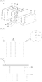
- FIG. 1 is an exploded perspective view showing the display device 100 according to one embodiment of the present disclosure.
- the display device 100 of the present disclosure includes a display panel 110, a middle frame 120, a multi-layer panel 130, a metal plate 140, and a rear cover 150.
- the display panel 110 may serveto output an image on a screen. More specifically, the display panel 110 divides an image into a plurality of pixels to digitalize information, such as color, brightness, chroma, etc., on a per pixel basis into electric signals, thereby controlling emission of light from the pixels to output an image having desired color, brightness and chroma based on the electric signals.
- information such as color, brightness, chroma, etc.
- Flat panel display devices having the above-described image output function may be utilized in various ways in liquid crystal display, thin film transistor liquid crystal display, organic light emitting diode (OLED) display fields.
- OLED organic light emitting diode
- a configuration is simplified and omission of a support structure is necessary to achieve a reduced thickness and greater heat radiation.
- the middle frame 120 may serve to provide a finished look around the periphery of the display device 100 and to align the display panel 110 and the multi-layer panel 130 with each other.
- a top case configured to cover a front surface and a rear case configured to cover a rear surface may be provided individually, in order to reduce the thickness of the display device 100, and to provide a simplified configuration as well as a reduction in the size of a bezel, the middle frame 120 may beused instead of the top case that covers the front surface.
- the multi-layer panel 130 may beattached to a rear surface of the display panel 110 to support the display panel 110. Reduction in the thickness of the display device 100 causes reduction in the thickness of a rear panel that supports the rear surface of the display panel 110. An excessively reduced thickness of the rear panel may reduce rigidity and increase possibility of deformation, whereas an excessively increased thickness of the rear panel may increase the weight and manufacturing costs.
- the multi-layer panel 130 may be used as the rear panel.
- the multi-layer panel 130 may providesufficient rigidity while minimizing increase in weight.
- the multi-layer panel 130 may have a triple layered configuration consisting of a pair of thin plates 131 and 132 and a honeycomb mesh 135 interposed between the thin plates 131 and 132.
- the honeycomb mesh 135 is configured such that a plurality of unit cells in the form of empty hexagonal shapes may be arranged in a plurality of columns to produce a honeycomb structure or pattern. Sidewalls of the unit cells and the thin plates 131 and 132 are oriented to face in different directions. For example, the sidewalls of the unit cells may be perpendicular to the thin plates 131 and 132. As such, the unit cells may serve to provide added rigidity and prevent bending of the display device 110. As compared to a conventional monolayer rear panel, the multi-layer panel 130 may have a smaller weight and achieve greater rigidity despite use of a reduced amount of material. Due to the honeycomb pattern mesh and thin metal plate layers, the multi-layered plate 130 may also be referred to herein as a sandwich honeycomb panel.
- the multi-layer panel 130 and the display panel 110 may be attached to each other with an adhesive layer 115 interposed therebetween.
- the adhesive layer 115 may be formed by applying an adhesive, or may be formed of a double-sided adhesive tape.
- the adhesive layer 115 may be laminated on the entire rear surface of the display panel 110, or the adhesive layer 115 may be laminated only on a part of the rear surface.
- the metal plate 140 may beattached to a rear surface of the multi-layer panel 130, and drive boards 147, 148 and 149 (see Figure 11 )may beseated on the metal plate 140.
- the metal plate 140 may be configured to cover the entire rear surface or a partial region of the multi-layer panel 130.
- Themetal plate 140 may have a size required to support the drive boards 147, 148 and 149 arranged thereon, and thus may cover only a part of the rear surface of the multi-layer panel 130.
- the metal plate 140 may be formed of a metal material, such as aluminum, to achieve rigidity of the display device 100 and to radiate heat generated from the drive boards 147, 148 and 149. To reduce bending deformation, reinforcement ribs may be formed at a center region of the metal plate 140.
- the drive boards 147, 148 and 149 seated on the metal plate 140 may include three types.
- the power supply board 147 may be ahardware that converts Alternating Current (AC) received from an external source into Direct Current (DC) that will be stably used by the display device 100, so as to supply power suitable for each system. If the power supply board 147 fails to stably supply power to the system, the system may be down or may malfunction.
- the power supply board 147 may bedivided into an electromagnetic interference filter part, an AC-DC rectifier part, a DC-AC switching converter part, and an output part, and may emit a great quantity of heat during driving.
- the main board 148 may serve to control the display panel 110 to generate a screen image and to control general functions of respective components. As functions of the display device 100 have recently been diversified, the number of elements mounted on the main board 148 has increased, and functions of the respective elements become important.
- the timing controller 149 may beprovided to a large screen of 10 inches or more, and may include semiconductors that adjust the quantity of data to be transmitted to the drive unit of the display panel 110 and improve resolution of an image.
- the timing controller 149 receives image information and transmits the same to the drive unit of the display panel 110 such that the entire display panel 110 outputs an image with no time difference.
- timing controller 149 adjusts transmission time of signals.
- the power supply board 147 and the main board 148 generate a great quantity of heat, and thus a region affected by both the power supply board 147 and the main board 148 has a relatively high temperature. That is, a place where the power supply board 147 and the main board 148 are located generates a great quantity of heat, and radiation of heat is important to the corresponding regions.
- the metal plate 140 or the multi-layer panel 130 which are formed of a metal material, have a high rate of thermal expansion, whereas the display panel 110 has a low rate of thermal expansion. Such difference between the rates of thermal expansion of the respective members causes the member having a lower rate of thermal expansion to be concavely bent as temperature increases.
- the multi-layer panel 130 has a higher rate of thermal expansion than that of the display panel 110, if heat is generated during driving of the display device 100, both ends of the display panel 110 are bent forward, causing a front surface of the display panel 110 to be concavely deformed. In current situation in which sizes of flat display devices 100 is increasing, such bending deformation may beeasily noticeable. Therefore, it is necessary to prevent this bending deformation.
- the present disclosure has a feature in that, to compensate for thermal deformation due to difference between rates of thermal expansion of the respective members during thermal expansion, a rigid bar may be provided to compensate for structural deformation of the multi-layer panel 130 and the metal plate 140.
- a rigid bar may be provided to compensate for structural deformation of the multi-layer panel 130 and the metal plate 140.
- FIG. 2 is a rear view showing the thin front plate 131 of the display device 100 according to one embodiment of the present disclosure.
- the thin front plate 131 has an opening perforated in a direction parallel to a short side of the display device 100 (e.g., vertical direction). Since effects of thermal expansion appears more in a longer side direction, bending deformation occurs in the longer side direction to a greater degree. Accordingly, to compensate for deformation in the longer side direction, the opening is formed in a direction perpendicular to a longer side.
- the horizontal direction refers to a direction parallel to a long side and the vertical direction refers to a direction parallel to a short side. It should be appreciated, however, that the present disclosure is applicable for display panels having various shapes, including those which are longer height than width.
- the opening may include a plurality of holes 131a aligned in a vertical direction to define a plurality of vertical lines 131b horizontally spaced apart from one another.Each line 131b may extend from the top to the bottom as exemplarily shown in Figure 2 , or may extend from the top to a middle point or from the bottom to the middle point such that upper half lines and lower half lines are alternately arranged rather than being connected to each other as exemplarily shown in Figure3 .
- the opening may include elongated slots.
- the thin front plate 131 thermally expands in response to temperature increase, the size of the opening may be reduced to cancel a variation in length due to thermal expansion. As such, it is possible to reduce length variation of the multi-layer panel 130 that exhibits greater length variation than the display panel 110.
- the thin rear plate 132 may include an opening consisting of vertically aligned holes 132a to define a plurality of lines 132b horizontally spaced apart from one another.
- the respective lines 131b may be arranged equidistant from each other in the same manner as the above-described thin front plate 131, as exemplarily shown in Figure 5 , the lines may be more densely arranged in a center region that is most susceptible to the bending deformation. Alternatively, the interval between the lines 132b of the thin rear plate 132 may be more reduced at a portion where elements that emit a large amount ofheat are located.
- the thin front plate 131 may becovered by the thin rear plate 132 and the display panel 110, and therefore may haveless restriction as to a position of the opening.
- the metal plate 140 and the rear cover 150 are sized to cover only a part of the multi-layer panel 130, a part of the thin rear plate 132 may beexposed reward of the display device 100.
- the opening may be formed only in a region covered by the metal plate 140 and the rear cover 150.
- Figures 6 and 7 are rear views showing the metal plate 140 of the display device 100 according to the present disclosure.
- the metal plate 140 may include a plurality of vertically aligned holes 141a, and a plurality of lines 141b, each of which includes the plurality of holes 141a, may be horizontally spaced apart from one another.
- the lines 141b may be arranged at a constant interval, or may be densely arranged at a region where the greatest amount of heat is generated, or may be more densely arranged at a center region where the greatest amount of bending deformation occurs. That is, the density of the lines 141b near the central region of the display may be greater than a density of the lines 141b near lateral regions of the display.
- a plurality of segment plates 142 may be arranged in a longer side direction.
- the segment plates 142 may be spaced apart from one another, and therefore gaps between the segment plates 142 compensate for increase in the length of each segment plate 142, which may substantially prevent deformation of the metal plate 140 from having an effect on bending deformation of the entire display device 100.
- Providing the multi-layer panel 130 and the metal plate 140, which are formed of metal materials and have greater rates of thermal deformation than the display panel 110, with the opening or the plurality of segment plates 142 may compensate for length variation due to thermal expansion.
- the adhesive layer 115 which is interposed between the display panel 110 and the multi-layer panel 130 to couple the display panel 110 and the multi-layer panel 130, may also undergo thermal expansion. However, unlike the display panel 110 or the multi-layer panel 130, the adhesive layer 115 is soft and is not bent even whenit is deformed.
- the display panel 110 may beless affected by thermal expansion of the multi-layer panel 130.
- the adhesive layer 115 may serve not only to attach the display panel 110 and the multi-layer panel 130 to each other, but also to cancel deformation of the multi-layer panel 130 during thermal expansion, thereby preventing bending of the display panel 110. Since the aforementioned two properties contradict each other, when considering only adhesive force, the adhesive layer 115 may be formed of a hard and highly adhesive material.
- the adhesive layer 115 may be provided to have a high elongation percentage in order to compensate for thermal expansion of the multi-layer panel 130 as described above. To sufficiently cancel out deformation of the multi-layer panel 130, the adhesive layer 115 may have an elongation percentage of about 800% or more.
- Figure 8 is a rear view of the adhesive layer 115 of the display device 100 according to the present disclosure.
- the adhesive layer 115 may be configured to cover the entire display panel 110 as exemplarily shown in Figure8A .
- the adhesive layer 115 exhibits increased adhesive force, which may cause the display panel 110 to be bent according to deformation of the multi-layer panel 130.
- the adhesive layer 115 may be easily extended.
- the adhesive layer 115 may be required to cover an area corresponding to 60% or more of the display panel 110 or the multi-layer panel 130because the area of the adhesive layer 115 is associated with coupling force between the display panel 110 and the multi-layer panel 130.
- the adhesive layer 115 may also be required to cover an area corresponding to 70% or more of the display panel 110 or the multi-layer panel 130.
- Figures8B, 8C and 8D show the adhesive layer 115 configured to cover a two-third area that of Figure8A . More specifically, a partial upper portion of the adhesive layer 115 may be omitted as exemplarily shown in Figure8B , or the adhesive layer 115 may be divided into a plurality of separate sections extending in a direction parallel to a shorter side as exemplarily shown in Figure8C . Alternatively, the adhesive layer 115 may be vertically and horizontally split into a plurality of separate sections as exemplarily shown in Figure8D .
- Figure 9 is a graph showing bending deformation depending on arrangement of the adhesive layer 115 of Figures 8A to 8D .
- the line shows variation of a bending deformation degree and the least amount of deformation occurs in the case of Figure8C .
- the case of Figure8C adopting horizontally split sections suitable to sufficiently cancel the horizontal deformation may be the most effective to prevent transfer of thermal expansion of the multi-layer panel 130 to the display panel 110.
- the adhesive layer 115 may include a double-sided tape.
- Figure 10 is a sectional view showing the double-sided tape 115 as one embodiment of the adhesive layer 115 of the display device 100 according to the present disclosure.
- the double-sided tape 115 may be formed by applying adhesive 115a to both surfaces of a resin layer 115b. If the resin layer 115b has a high elongation percentage, the double-sided tape 115 may have a high elongation percentage.
- the double-sided tape 115 including the porous resin layer 115b having pores 115c when using the double-sided tape 115 including the porous resin layer 115b having pores 115c, the double-sided tape 115 is more easily extended.
- the double-sided tape 115 including the porous resin layer 115b has four times greater elongation percentage than a double-sided tape formed of Carbon Fiber Reinforced Plastics (CFRP).
- CFRP Carbon Fiber Reinforced Plastics
- Figure 11 is a rear view showing a separated state of the rear cover 150 of the display device 100 according to the present disclosure
- Figure 12 is a sectional view taken along the line A-A' of Figure 11 .
- a rigid bar 160 may be further provided at the rear surface of the multi-layer panel 130 so as to extend in a horizontal direction. The rigid bar 160 may prevent the front surface of the display panel 110 from being concavely bent.
- the rigid bar 160 is a bar-shaped member and is formed of a material that is not easily bent.
- the rigid bar 160 may be fixed to PEM nuts161 (or self-clinching nut), which may beinserted into the multi-layer panel 130 to protrude from a rear surface of the metal plate 140, via screws 163.
- Figure 12 is a sectional view showing a state in which the display panel 110 and the multi-layer panel 130 are coupled to the rigid bar 160 so as to centrally protrude forward at a center region thereof and protrude rearward at left and right ends thereof.
- a PEM nut 161a located at the center region of the display and a PEM nut 161b located at a side region may have different lengths.
- the rigid bar 160 having a slightly bulged front surface may be fixed to the display panel 110 and the multi-layer panel 130.
- the rigid bar 160 or the multi-layer panel 130 may be kept in a bent state. Since the rigid bar 160 is harder than the multi-layer panel 130, the multi-layer panel 130 is originally kept in a bent state. Therefore, before the display device 100 is driven, as exemplarily shown in Figure 12 , the multi-layer panel 130 slightly protrudes forward by a height difference a between the PEM nuts 161a and 161b.
- the front surface of the multi-layer panel 130 begins to be concavely deformed due to thermal expansion of the multi-layer panel 130 as the temperature of the display device 100 increase.
- such concave deformation of the front surface of the multi-layer panel 130 occurs in a state in which force has previously been applied in a direction opposite to the above deformation caused by thermal expansion such that the center region of the front surface of the multi-layer panel 130 slightly protrudes forward owing to provision of the rigid bar 160 and the PEM nuts 161a and 161b having a height difference. Therefore, after the multi-layer panel 130 has completely been deformed due to thermal expansion, the multi-layer panel 130 exhibits less deformation than the case in which the rigid bar 160 is not used.
- the above Table 1 shows a deformation degree of the panel depending on power consumption of the display device 100.
- a temperature difference of about 1°C occurs per 10W.
- a height difference between the PEM nut 161b located at the end and the PEM nut 161a located at the center region is 2mm, the front surface of the display device 100 is concavely deformed even when power consumption is 282W, and thus deviation between the end and the center region is only 2mm.
- the opening formed in the multi-layer panel 130 may be reduced in size to compensate for deformation of the multi-layer panel 130 due to thermal expansion, which may minimize increase in the length of the entire multi-layer panel 130.
- the adhesive layer 115 may bepossible to substantially prevent thermal expansion of the multi-layer panel 130 from having a negative effect on the display panel 110, which may minimize concave deformation of the front surface of the display device 100.
- the present disclosure is directed to a display device that substantially obviates one or more problems due to limitations and disadvantages of the related art.
- Oneobject of the present disclosure is to provide a display device having a sandwich honeycomb panel to minimize bending deformation due to thermal expansion.
- a display device may include a display panel, a sandwich honeycomb panel including a thin front plate located toward the display panel, a thin rear plate disposed on a rear surface of the thin front plate, and a honeycomb mesh interposed between the thin front plate and the thin rear plate, the honeycomb mesh having a plurality of hexagonal unit cells, and a metal plate coupled to a rear surface of the sandwich honeycomb panel such that a drive board is seated on the metal plate, wherein at least one of the thin front plate or the thin rear plate includes at least one opening formed parallel to a shorter side of the display device.
- the opening may include a plurality of holes arranged parallel to the shorter side.
- the opening may be a slit extending in a direction parallel to the shorter side.
- the at least one opening may include a plurality of openings spaced apart from one another in a direction parallel to a longer side of the display device.
- Distances between the openings may be reduced at a center region of the display device and may be increased at both ends of the display device.
- the display device mayfurther include a rear cover coupled to the rear surface of the sandwich honeycomb panel, and the opening of the thin rear plate may be formed only in a portion of the thin rear plate covered by the rear cover.
- the metal plate may include an opening formed parallel to the shorter side of the display device.
- the metal plate may further include a plurality of segment plates arranged in a direction parallel to a longer side of the display device, and the segment plates may be spaced apart from one another.
- the display device may further include an adhesive layer interposed between the display panel and the sandwich honeycomb panel, and the adhesive layer may be divided into a plurality of sections so as to be separately arranged in a plurality of regions of a rear surface of the display panel.
- the sections of the adhesive layer may be spaced apart from one another in a direction parallel to a longer side of the display device.
- An area of the adhesive layer may be less than 60% or 70% of an area of the display panel.
- the adhesive layer may be a double-sided tape formed by applying adhesive to both surfaces of a porous resin layer.
- the adhesive layer may have an elongation percentage of about 800% or more.
- the display device may further include a plurality of PEM nuts arranged on a rear surface of the metal plate in a direction parallel to a longer side of the display device, and a rigid bar coupled to the rear surface of the metal plate via screws inserted into the PEM nuts.
- a height of the PEM nuts located at both ends of the display device may be less than a height of the PEM nut located at another position.
- a display device may include a display panel, a multi-layered panel provided adjacent the display panel and including a front plate located toward the display panel, a rear plate provided parallel to the front plate, and a honeycomb pattern mesh interposed between the front plate and the rear plate, the honeycomb pattern mesh having a plurality of hexagonal cells to form a honeycomb pattern, and a metal plate coupled to a rear surface of the multi-layered panel and a drive board provided on the metal plate.
- At least one of the front plate or the rear plate may include at least one opening that extends parallel to a shorter side of the display device.
- the opening may include a plurality of holes which are arranged in a line that extends parallel to the shorter side.
- the opening may be a slit formed through the front plate or the rear plate that extends parallel to the shorter side.
- a plurality of the openings may be provided to be spaced apart from one another in a direction parallel to a longer side of the display device.
- the openings in a central region of the display device may be arranged a first distance from each other and the openings at lateral regions of the display device may be arranged a second distance from each other, the second distance being greater than the first distance.
- a rear cover may be provided coupled to the rear surface of the multi-layered panel, wherein the at least one opening provided on the rear plate is formed only in a region of the rear plate covered by the rear cover.
- the metal plate may include at least one opening formed parallel to the shorter side of the display device.
- the metal plate may include a plurality of segment plates arranged in a direction parallel to a longer side of the display device, and wherein the segment plates are spaced apart a prescribed distance from one another.
- An adhesive layer may be interposed between the display panel and the multi-layered panel, wherein the adhesive layer is divided into a plurality of sections which are each arranged separately in a plurality of regions of a rear surface of the display panel.
- the sections of the adhesive layer may bespaced apart from one another in a direction parallel to a longer side of the display device.
- An area of the adhesive layer may beless than 60% or 70% of an area of the display panel.
- the adhesive layer may bea double-sided tape that includes a porous resin layer and an adhesive provided on both surfaces of the porous resin layer.
- the adhesive layer may bean elongation percentage of about 800% or more.
- a plurality of PEM nuts may be arranged on a rear surface of the metal plate, and a bar may be provided on the rear surface of the metal plate parallel to a longer side of the display device and positioned to correspond to the PEM nuts, the bar being coupled to the rear surface of the metal plate by screws inserted into the PEM nuts.
- a height of the PEM nuts located in lateral regions of the display device may beless than a height of the PEM nut located in other regions.
- a display device may include a display panel, an adhesive layer having a prescribed pattern provided on a rear surface of the display panel, a multi-layered panel coupled to the display panel by the adhesive layer, the multi-layered panel including a mesh panel layer having a honeycomb pattern, a metal plate provided adjacent the multi-layered panel, a bar provided on the metal plate, and a rear cover provided to cover the metal plate.
- the display panel may have a first rate of thermal expansion
- the multi-layered panel may have a second rate of thermal expansion
- the metal plate may have a third rate of thermal expansion.
- the multi-layered panel and the metal plate may thermally expand at a greater rate than the display panel with respect to temperature.
- the multi-layered panel may include a first metal panel layer, a second metal panel layer, and the mesh panel layer may be provided between the first and second metal panel layers, the mesh panel layer having a plurality of hexagonal regions provided adjacent to each other to form the honeycomb pattern.
- At least one of the multi-layered panel or the metal plate may include a plurality of holes, the plurality of holes aligned to form a plurality of vertical lines which are provided a prescribed distance from an adjacent vertical line of holes.
- a density of the plurality of vertical lines may be greater in a central region of the display panel than a lateral region of the display panel.
- the bar may be provided horizontally across the metal plate and configured to bend the display panel to have a prescribed amount of convex curvature, the prescribed amount of convex curvature corresponding to an amount of deformation of the display panel caused by thermal expansion.
- any reference in this specification to "one embodiment,” “an embodiment,” “example embodiment,” etc. means that a particular feature, structure, or characteristic described in connection with the embodiment is included in at least one embodiment of the invention.
- the appearances of such phrases in various places in the specification are not necessarily all referring to the same embodiment.
Landscapes
- Engineering & Computer Science (AREA)
- Theoretical Computer Science (AREA)
- Physics & Mathematics (AREA)
- General Physics & Mathematics (AREA)
- Computer Hardware Design (AREA)
- General Engineering & Computer Science (AREA)
- Microelectronics & Electronic Packaging (AREA)
- Human Computer Interaction (AREA)
- Thermal Sciences (AREA)
- Devices For Indicating Variable Information By Combining Individual Elements (AREA)
Claims (13)
- Eine Anzeigevorrichtung (100), umfassend:eine Anzeigetafel (110);ein mehrlagiges Paneel (130), das benachbart zu der Anzeigetafel (110) vorgesehen ist und eine in Richtung der Anzeigetafel (110) gelegene Frontplatte (131), eine parallel zu der Frontplatte (131) vorgesehene Rückplatte (132) sowie ein zwischen der Frontplatte (131) und der Rückplatte (132) angeordnetes Honigwabenmuster-Gitter (135) aufweist, wobei das Honigwabenmuster-Gitter (135) eine Mehrzahl von hexagonalen Zellen aufweist, um ein Honigwabenmuster zu bilden; undeine Metallplatte (140), die mit einer Rückfläche des mehrlagigen Paneels (130) gekoppelt ist, sowie eine auf der Metallplatte (140) vorgesehene Antriebsplatte (147, 148, 149),dadurch gekennzeichnet, dassdie Frontplatte (131) und/oder die Rückplatte (132) eine Mehrzahl von Öffnungen (131a, 132a) aufweist, die sich parallel zu einer kürzeren Seite der Anzeigevorrichtung (100) erstrecken, wobei eine Mehrzahl der Öffnungen (131a, 132a) in einer Richtung parallel zu einer längeren Seite der Anzeigevorrichtung (100) voneinander beabstandet angeordnet ist, und wobei Öffnungen (131a, 132a) in einem mittigen Bereich in einer Richtung parallel zu einer längeren Seite der Anzeigevorrichtung (100) in einem ersten Abstand voneinander beabstandet sind und Öffnungen in Bereichen seitlich des mittigen Bereichs in einer Richtung parallel zu der längeren Seite der Anzeigevorrichtung (100) in einem zweiten Abstand voneinander beabstandet sind und der zweite Abstand größer als der erste Abstand ist.
- Anzeigevorrichtung (100) nach Anspruch 1, wobei jede der Öffnungen eine Mehrzahl von Löchern (131a, 132a) aufweist, die in einer Linie angeordnet sind, die sich parallel zu der kürzeren Seite erstreckt.
- Anzeigevorrichtung (100) nach Anspruch 1, wobei jede der Öffnungen ein durch die Frontplatte (131) oder die Rückplatte (132) hindurch gebildeter Schlitz ist, der sich parallel zu der kürzeren Seite erstreckt.
- Anzeigevorrichtung (100) nach einem der Ansprüche 1 bis 3, ferner aufweisend eine Rückabdeckung (150), die mit der Rückfläche des mehrlagigen Paneels (130) gekoppelt ist, wobei die an der Rückplatte (132) vorgesehenen Öffnungen nur in einem Bereich der Rückplatte (132) gebildet sind, der von der Rückabdeckung (150) abgedeckt ist.
- Anzeigevorrichtung (100) nach einem der Ansprüche 1 bis 4, wobei die Metallplatte (140) mindestens eine Öffnung aufweist, die parallel zu der kürzeren Seite der Anzeigevorrichtung (100) ausgebildet ist.
- Anzeigevorrichtung (100) nach einem der Ansprüche 1 bis 5, wobei die Metallplatte (140) eine Mehrzahl von Segmentplatten (142) aufweist, die in einer Richtung parallel zu einer längeren Seite der Anzeigevorrichtung (100) angeordnet sind, und wobei die Segmentplatten (142) voneinander um einen vorgegebenen Abstand beabstandet sind.
- Anzeigevorrichtung (100) nach einem der Ansprüche 1 bis 6, ferner aufweisend eine Haftvermittlerschicht (115), die zwischen der Anzeigetafel (110) und dem mehrlagigen Paneel (130) vorgesehen ist, wobei die Haftvermittlerschicht (115) in eine Mehrzahl von Abschnitten unterteilt ist, die in einer Mehrzahl von Bereichen einer Rückfläche der Anzeigevorrichtung (110) jeweils separat angeordnet sind.
- Anzeigevorrichtung (100) nach Anspruch 7, wobei die Abschnitte der Haftvermittlerschicht (115) in einer Richtung parallel zu einer längeren Seite der Anzeigevorrichtung (100) voneinander beabstandet sind.
- Anzeigevorrichtung (100) nach Anspruch 7 oder 8, wobei ein Bereich der Haftvermittlerschicht (115) weniger als 60% oder 70% einer Fläche der Anzeigetafel (110) ausmacht.
- Anzeigevorrichtung (100) nach einem der Ansprüche 7 bis 9, wobei die Haftvermittlerschicht (115) ein doppelseitiges Klebeband ist, das eine poröse Harzschicht (115b) sowie einen Haftvermittler (115a) aufweist, der auf beiden Oberflächen der porösen Harzschicht (115b) vorgesehen ist.
- Anzeigevorrichtung (100) nach einem der Ansprüche 7 bis 10, wobei die Haftvermittlerschicht (115) eine prozentuale Dehnung von etwa 800% oder mehr aufweist.
- Anzeigevorrichtung (100) nach einem der Ansprüche 1 bis 11, ferner aufweisend eine Mehrzahl von PEM-Muttern (161), die auf einer Rückfläche der Metallplatte (140) angeordnet sind, sowie einen Steg (160), der auf der Rückfläche der Metallplatte (150) parallel zu einer längeren Seite der Anzeigevorrichtung (100) vorgesehen und den PEM-Muttern (161) entsprechend positioniert ist, wobei der Steg (160) mittels in die PEM-Muttern (161) eingeschraubter Schrauben (163) an die Rückfläche der Metallplatte (150) gekoppelt ist.
- Anzeigevorrichtung (100) nach Anspruch 12, wobei eine Höhe der in seitlichen Bereichen der Anzeigevorrichtung (100) gelegenen PEM-Muttern (161) geringer ist als eine Höhe der in anderen Bereichen gelegenen PEM-Muttern (161).
Applications Claiming Priority (2)
| Application Number | Priority Date | Filing Date | Title |
|---|---|---|---|
| KR1020130080262A KR102174635B1 (ko) | 2013-07-09 | 2013-07-09 | 디스플레이 장치 |
| PCT/KR2013/009200 WO2015005533A1 (en) | 2013-07-09 | 2013-10-15 | Display device |
Publications (3)
| Publication Number | Publication Date |
|---|---|
| EP3020035A1 EP3020035A1 (de) | 2016-05-18 |
| EP3020035A4 EP3020035A4 (de) | 2017-01-04 |
| EP3020035B1 true EP3020035B1 (de) | 2018-01-10 |
Family
ID=52276911
Family Applications (1)
| Application Number | Title | Priority Date | Filing Date |
|---|---|---|---|
| EP13889182.5A Active EP3020035B1 (de) | 2013-07-09 | 2013-10-15 | Anzeigevorrichtung |
Country Status (5)
| Country | Link |
|---|---|
| US (2) | US9635787B2 (de) |
| EP (1) | EP3020035B1 (de) |
| KR (1) | KR102174635B1 (de) |
| CN (1) | CN105359204B (de) |
| WO (1) | WO2015005533A1 (de) |
Families Citing this family (6)
| Publication number | Priority date | Publication date | Assignee | Title |
|---|---|---|---|---|
| KR102423659B1 (ko) * | 2017-09-25 | 2022-07-22 | 엘지전자 주식회사 | 디스플레이 디바이스 |
| CN110706591A (zh) * | 2019-09-02 | 2020-01-17 | 武汉华星光电半导体显示技术有限公司 | 显示装置 |
| JP7598263B2 (ja) * | 2021-03-01 | 2024-12-11 | シャープ株式会社 | 表示装置 |
| KR20230156740A (ko) * | 2021-03-15 | 2023-11-14 | 엘지전자 주식회사 | 디스플레이 디바이스 |
| JP7715590B2 (ja) * | 2021-09-27 | 2025-07-30 | 新光電気工業株式会社 | 配線基板及び配線基板の製造方法 |
| US20240260217A1 (en) * | 2021-12-20 | 2024-08-01 | Lg Electronics Inc. | Display device |
Family Cites Families (15)
| Publication number | Priority date | Publication date | Assignee | Title |
|---|---|---|---|---|
| JP4650821B2 (ja) * | 2001-04-23 | 2011-03-16 | パナソニック株式会社 | ディスプレイ装置 |
| JP4547168B2 (ja) * | 2003-03-03 | 2010-09-22 | 昭和電工株式会社 | 二次元ディスプレイ装置用放熱器の製造方法 |
| JP2005141194A (ja) * | 2003-10-14 | 2005-06-02 | Seiko Epson Corp | 補強構造体、表示装置、及び電子機器 |
| WO2006098365A1 (ja) * | 2005-03-15 | 2006-09-21 | Matsushita Electric Industrial Co., Ltd. | 表示装置 |
| KR100770128B1 (ko) * | 2005-07-26 | 2007-10-24 | 삼성에스디아이 주식회사 | 플라즈마 디스플레이 장치 |
| KR20080054681A (ko) | 2006-12-13 | 2008-06-19 | 이종환 | 록크 너트 |
| JP5157200B2 (ja) * | 2007-03-08 | 2013-03-06 | 株式会社リコー | ハニカム構造シートの製造方法及び表示パネルの製造方法 |
| WO2008129717A1 (ja) * | 2007-03-30 | 2008-10-30 | Sharp Kabushiki Kaisha | 光学部材、照明装置、表示装置、及びテレビ受信装置 |
| KR20090128761A (ko) * | 2008-06-11 | 2009-12-16 | 엘지전자 주식회사 | 디스플레이 장치 |
| JP5374166B2 (ja) * | 2009-01-09 | 2013-12-25 | キヤノン株式会社 | 薄型パネル表示装置 |
| CN201667186U (zh) * | 2010-04-14 | 2010-12-08 | 深圳市显科科技有限公司 | 一种户外全天候led显示屏的箱体结构 |
| WO2013100690A1 (en) * | 2011-12-30 | 2013-07-04 | Samsung Electronics Co., Ltd. | Display device |
| KR101945890B1 (ko) * | 2011-12-30 | 2019-02-12 | 삼성전자주식회사 | 디스플레이 장치 |
| CN202549200U (zh) * | 2012-04-19 | 2012-11-21 | 厦门飓浪计算机软件有限公司 | 一种自助终端计算机的显示屏 |
| JP6195698B2 (ja) * | 2012-06-11 | 2017-09-13 | サターン ライセンシング エルエルシーSaturn Licensing LLC | 表示装置 |
-
2013
- 2013-07-09 KR KR1020130080262A patent/KR102174635B1/ko active Active
- 2013-10-15 CN CN201380078106.7A patent/CN105359204B/zh active Active
- 2013-10-15 EP EP13889182.5A patent/EP3020035B1/de active Active
- 2013-10-15 WO PCT/KR2013/009200 patent/WO2015005533A1/en not_active Ceased
- 2013-10-24 US US14/062,021 patent/US9635787B2/en active Active
-
2017
- 2017-03-13 US US15/457,363 patent/US10499548B2/en active Active
Non-Patent Citations (1)
| Title |
|---|
| None * |
Also Published As
| Publication number | Publication date |
|---|---|
| CN105359204B (zh) | 2019-12-17 |
| KR102174635B1 (ko) | 2020-11-05 |
| US20150016032A1 (en) | 2015-01-15 |
| EP3020035A1 (de) | 2016-05-18 |
| CN105359204A (zh) | 2016-02-24 |
| KR20150006635A (ko) | 2015-01-19 |
| US10499548B2 (en) | 2019-12-03 |
| EP3020035A4 (de) | 2017-01-04 |
| US20170188489A1 (en) | 2017-06-29 |
| US9635787B2 (en) | 2017-04-25 |
| WO2015005533A1 (en) | 2015-01-15 |
Similar Documents
| Publication | Publication Date | Title |
|---|---|---|
| US10499548B2 (en) | Display device | |
| US8634042B2 (en) | Liquid crystal display with a plurality of liquid crystal display modules | |
| CN102818193B (zh) | 一种直下式led背光模组及其显示装置 | |
| RU2586451C1 (ru) | Устройство отображения | |
| KR102040612B1 (ko) | 디스플레이 장치 | |
| US9720269B2 (en) | Display device | |
| CN104197240A (zh) | 曲率可调的复合背板及背光模块 | |
| EP2837963B1 (de) | Rückbeleuchtungseinheit für Anzeigevorrichtung | |
| US20190146263A1 (en) | Display device | |
| KR101318933B1 (ko) | 백라이트 장치, 화상 표시 장치 및 백라이트 장치의 조립 방법 | |
| US10025126B2 (en) | Display device | |
| JP2003279978A (ja) | 液晶表示装置 | |
| JP5527230B2 (ja) | バックライト装置及び画像表示装置 | |
| KR20140141292A (ko) | 샌드위치 허니컴 패널을 이용한 디스플레이 장치 | |
| KR102480835B1 (ko) | 백라이트 유닛 및 이를 포함하는 표시 장치 | |
| KR20150006634A (ko) | 디스플레이 장치 | |
| KR102043307B1 (ko) | 표시장치 | |
| KR20060073866A (ko) | 액정 표시 모듈 | |
| KR102081120B1 (ko) | 백 라이트 유닛 및 이를 이용한 액정 표시장치 | |
| KR102364342B1 (ko) | 광원 모듈 및 이를 포함하는 백라이트 유닛과 액정 표시 장치 | |
| KR20130019224A (ko) | 백라이트 유닛 및 이를 구비한 액정표시장치 | |
| JP2014081435A (ja) | 両面表示装置 |
Legal Events
| Date | Code | Title | Description |
|---|---|---|---|
| PUAI | Public reference made under article 153(3) epc to a published international application that has entered the european phase |
Free format text: ORIGINAL CODE: 0009012 |
|
| 17P | Request for examination filed |
Effective date: 20160112 |
|
| AK | Designated contracting states |
Kind code of ref document: A1 Designated state(s): AL AT BE BG CH CY CZ DE DK EE ES FI FR GB GR HR HU IE IS IT LI LT LU LV MC MK MT NL NO PL PT RO RS SE SI SK SM TR |
|
| AX | Request for extension of the european patent |
Extension state: BA ME |
|
| DAX | Request for extension of the european patent (deleted) | ||
| A4 | Supplementary search report drawn up and despatched |
Effective date: 20161205 |
|
| RIC1 | Information provided on ipc code assigned before grant |
Ipc: G09F 9/30 20060101ALI20161129BHEP Ipc: G09F 9/00 20060101AFI20161129BHEP |
|
| GRAP | Despatch of communication of intention to grant a patent |
Free format text: ORIGINAL CODE: EPIDOSNIGR1 |
|
| INTG | Intention to grant announced |
Effective date: 20170802 |
|
| GRAS | Grant fee paid |
Free format text: ORIGINAL CODE: EPIDOSNIGR3 |
|
| GRAA | (expected) grant |
Free format text: ORIGINAL CODE: 0009210 |
|
| AK | Designated contracting states |
Kind code of ref document: B1 Designated state(s): AL AT BE BG CH CY CZ DE DK EE ES FI FR GB GR HR HU IE IS IT LI LT LU LV MC MK MT NL NO PL PT RO RS SE SI SK SM TR |
|
| REG | Reference to a national code |
Ref country code: CH Ref legal event code: EP Ref country code: AT Ref legal event code: REF Ref document number: 963203 Country of ref document: AT Kind code of ref document: T Effective date: 20180115 |
|
| REG | Reference to a national code |
Ref country code: IE Ref legal event code: FG4D |
|
| REG | Reference to a national code |
Ref country code: DE Ref legal event code: R096 Ref document number: 602013032022 Country of ref document: DE |
|
| REG | Reference to a national code |
Ref country code: NL Ref legal event code: MP Effective date: 20180110 |
|
| REG | Reference to a national code |
Ref country code: AT Ref legal event code: MK05 Ref document number: 963203 Country of ref document: AT Kind code of ref document: T Effective date: 20180110 |
|
| PG25 | Lapsed in a contracting state [announced via postgrant information from national office to epo] |
Ref country code: NL Free format text: LAPSE BECAUSE OF FAILURE TO SUBMIT A TRANSLATION OF THE DESCRIPTION OR TO PAY THE FEE WITHIN THE PRESCRIBED TIME-LIMIT Effective date: 20180110 |
|
| PG25 | Lapsed in a contracting state [announced via postgrant information from national office to epo] |
Ref country code: NO Free format text: LAPSE BECAUSE OF FAILURE TO SUBMIT A TRANSLATION OF THE DESCRIPTION OR TO PAY THE FEE WITHIN THE PRESCRIBED TIME-LIMIT Effective date: 20180410 Ref country code: LT Free format text: LAPSE BECAUSE OF FAILURE TO SUBMIT A TRANSLATION OF THE DESCRIPTION OR TO PAY THE FEE WITHIN THE PRESCRIBED TIME-LIMIT Effective date: 20180110 Ref country code: CY Free format text: LAPSE BECAUSE OF FAILURE TO SUBMIT A TRANSLATION OF THE DESCRIPTION OR TO PAY THE FEE WITHIN THE PRESCRIBED TIME-LIMIT Effective date: 20180110 Ref country code: ES Free format text: LAPSE BECAUSE OF FAILURE TO SUBMIT A TRANSLATION OF THE DESCRIPTION OR TO PAY THE FEE WITHIN THE PRESCRIBED TIME-LIMIT Effective date: 20180110 Ref country code: HR Free format text: LAPSE BECAUSE OF FAILURE TO SUBMIT A TRANSLATION OF THE DESCRIPTION OR TO PAY THE FEE WITHIN THE PRESCRIBED TIME-LIMIT Effective date: 20180110 Ref country code: FI Free format text: LAPSE BECAUSE OF FAILURE TO SUBMIT A TRANSLATION OF THE DESCRIPTION OR TO PAY THE FEE WITHIN THE PRESCRIBED TIME-LIMIT Effective date: 20180110 |
|
| PG25 | Lapsed in a contracting state [announced via postgrant information from national office to epo] |
Ref country code: GR Free format text: LAPSE BECAUSE OF FAILURE TO SUBMIT A TRANSLATION OF THE DESCRIPTION OR TO PAY THE FEE WITHIN THE PRESCRIBED TIME-LIMIT Effective date: 20180411 Ref country code: BG Free format text: LAPSE BECAUSE OF FAILURE TO SUBMIT A TRANSLATION OF THE DESCRIPTION OR TO PAY THE FEE WITHIN THE PRESCRIBED TIME-LIMIT Effective date: 20180410 Ref country code: PL Free format text: LAPSE BECAUSE OF FAILURE TO SUBMIT A TRANSLATION OF THE DESCRIPTION OR TO PAY THE FEE WITHIN THE PRESCRIBED TIME-LIMIT Effective date: 20180110 Ref country code: AT Free format text: LAPSE BECAUSE OF FAILURE TO SUBMIT A TRANSLATION OF THE DESCRIPTION OR TO PAY THE FEE WITHIN THE PRESCRIBED TIME-LIMIT Effective date: 20180110 Ref country code: RS Free format text: LAPSE BECAUSE OF FAILURE TO SUBMIT A TRANSLATION OF THE DESCRIPTION OR TO PAY THE FEE WITHIN THE PRESCRIBED TIME-LIMIT Effective date: 20180110 Ref country code: LV Free format text: LAPSE BECAUSE OF FAILURE TO SUBMIT A TRANSLATION OF THE DESCRIPTION OR TO PAY THE FEE WITHIN THE PRESCRIBED TIME-LIMIT Effective date: 20180110 Ref country code: SE Free format text: LAPSE BECAUSE OF FAILURE TO SUBMIT A TRANSLATION OF THE DESCRIPTION OR TO PAY THE FEE WITHIN THE PRESCRIBED TIME-LIMIT Effective date: 20180110 Ref country code: IS Free format text: LAPSE BECAUSE OF FAILURE TO SUBMIT A TRANSLATION OF THE DESCRIPTION OR TO PAY THE FEE WITHIN THE PRESCRIBED TIME-LIMIT Effective date: 20180510 |
|
| REG | Reference to a national code |
Ref country code: DE Ref legal event code: R097 Ref document number: 602013032022 Country of ref document: DE |
|
| PG25 | Lapsed in a contracting state [announced via postgrant information from national office to epo] |
Ref country code: AL Free format text: LAPSE BECAUSE OF FAILURE TO SUBMIT A TRANSLATION OF THE DESCRIPTION OR TO PAY THE FEE WITHIN THE PRESCRIBED TIME-LIMIT Effective date: 20180110 Ref country code: RO Free format text: LAPSE BECAUSE OF FAILURE TO SUBMIT A TRANSLATION OF THE DESCRIPTION OR TO PAY THE FEE WITHIN THE PRESCRIBED TIME-LIMIT Effective date: 20180110 Ref country code: IT Free format text: LAPSE BECAUSE OF FAILURE TO SUBMIT A TRANSLATION OF THE DESCRIPTION OR TO PAY THE FEE WITHIN THE PRESCRIBED TIME-LIMIT Effective date: 20180110 Ref country code: EE Free format text: LAPSE BECAUSE OF FAILURE TO SUBMIT A TRANSLATION OF THE DESCRIPTION OR TO PAY THE FEE WITHIN THE PRESCRIBED TIME-LIMIT Effective date: 20180110 |
|
| PLBE | No opposition filed within time limit |
Free format text: ORIGINAL CODE: 0009261 |
|
| STAA | Information on the status of an ep patent application or granted ep patent |
Free format text: STATUS: NO OPPOSITION FILED WITHIN TIME LIMIT |
|
| PG25 | Lapsed in a contracting state [announced via postgrant information from national office to epo] |
Ref country code: CZ Free format text: LAPSE BECAUSE OF FAILURE TO SUBMIT A TRANSLATION OF THE DESCRIPTION OR TO PAY THE FEE WITHIN THE PRESCRIBED TIME-LIMIT Effective date: 20180110 Ref country code: SM Free format text: LAPSE BECAUSE OF FAILURE TO SUBMIT A TRANSLATION OF THE DESCRIPTION OR TO PAY THE FEE WITHIN THE PRESCRIBED TIME-LIMIT Effective date: 20180110 Ref country code: DK Free format text: LAPSE BECAUSE OF FAILURE TO SUBMIT A TRANSLATION OF THE DESCRIPTION OR TO PAY THE FEE WITHIN THE PRESCRIBED TIME-LIMIT Effective date: 20180110 Ref country code: SK Free format text: LAPSE BECAUSE OF FAILURE TO SUBMIT A TRANSLATION OF THE DESCRIPTION OR TO PAY THE FEE WITHIN THE PRESCRIBED TIME-LIMIT Effective date: 20180110 |
|
| 26N | No opposition filed |
Effective date: 20181011 |
|
| PG25 | Lapsed in a contracting state [announced via postgrant information from national office to epo] |
Ref country code: SI Free format text: LAPSE BECAUSE OF FAILURE TO SUBMIT A TRANSLATION OF THE DESCRIPTION OR TO PAY THE FEE WITHIN THE PRESCRIBED TIME-LIMIT Effective date: 20180110 |
|
| REG | Reference to a national code |
Ref country code: CH Ref legal event code: PL |
|
| GBPC | Gb: european patent ceased through non-payment of renewal fee |
Effective date: 20181015 |
|
| REG | Reference to a national code |
Ref country code: BE Ref legal event code: MM Effective date: 20181031 |
|
| PG25 | Lapsed in a contracting state [announced via postgrant information from national office to epo] |
Ref country code: MC Free format text: LAPSE BECAUSE OF FAILURE TO SUBMIT A TRANSLATION OF THE DESCRIPTION OR TO PAY THE FEE WITHIN THE PRESCRIBED TIME-LIMIT Effective date: 20180110 Ref country code: LU Free format text: LAPSE BECAUSE OF NON-PAYMENT OF DUE FEES Effective date: 20181015 |
|
| REG | Reference to a national code |
Ref country code: IE Ref legal event code: MM4A |
|
| PG25 | Lapsed in a contracting state [announced via postgrant information from national office to epo] |
Ref country code: LI Free format text: LAPSE BECAUSE OF NON-PAYMENT OF DUE FEES Effective date: 20181031 Ref country code: BE Free format text: LAPSE BECAUSE OF NON-PAYMENT OF DUE FEES Effective date: 20181031 Ref country code: CH Free format text: LAPSE BECAUSE OF NON-PAYMENT OF DUE FEES Effective date: 20181031 Ref country code: FR Free format text: LAPSE BECAUSE OF NON-PAYMENT OF DUE FEES Effective date: 20181031 |
|
| PG25 | Lapsed in a contracting state [announced via postgrant information from national office to epo] |
Ref country code: GB Free format text: LAPSE BECAUSE OF NON-PAYMENT OF DUE FEES Effective date: 20181015 Ref country code: IE Free format text: LAPSE BECAUSE OF NON-PAYMENT OF DUE FEES Effective date: 20181015 |
|
| PG25 | Lapsed in a contracting state [announced via postgrant information from national office to epo] |
Ref country code: MT Free format text: LAPSE BECAUSE OF NON-PAYMENT OF DUE FEES Effective date: 20181015 |
|
| PG25 | Lapsed in a contracting state [announced via postgrant information from national office to epo] |
Ref country code: TR Free format text: LAPSE BECAUSE OF FAILURE TO SUBMIT A TRANSLATION OF THE DESCRIPTION OR TO PAY THE FEE WITHIN THE PRESCRIBED TIME-LIMIT Effective date: 20180110 |
|
| PG25 | Lapsed in a contracting state [announced via postgrant information from national office to epo] |
Ref country code: PT Free format text: LAPSE BECAUSE OF FAILURE TO SUBMIT A TRANSLATION OF THE DESCRIPTION OR TO PAY THE FEE WITHIN THE PRESCRIBED TIME-LIMIT Effective date: 20180110 |
|
| PG25 | Lapsed in a contracting state [announced via postgrant information from national office to epo] |
Ref country code: HU Free format text: LAPSE BECAUSE OF FAILURE TO SUBMIT A TRANSLATION OF THE DESCRIPTION OR TO PAY THE FEE WITHIN THE PRESCRIBED TIME-LIMIT; INVALID AB INITIO Effective date: 20131015 Ref country code: MK Free format text: LAPSE BECAUSE OF NON-PAYMENT OF DUE FEES Effective date: 20180110 |
|
| PGFP | Annual fee paid to national office [announced via postgrant information from national office to epo] |
Ref country code: DE Payment date: 20240905 Year of fee payment: 12 |