EP3012345A1 - Inorganic materials, methods and apparatus for making same, and uses thereof - Google Patents
Inorganic materials, methods and apparatus for making same, and uses thereof Download PDFInfo
- Publication number
- EP3012345A1 EP3012345A1 EP15175725.9A EP15175725A EP3012345A1 EP 3012345 A1 EP3012345 A1 EP 3012345A1 EP 15175725 A EP15175725 A EP 15175725A EP 3012345 A1 EP3012345 A1 EP 3012345A1
- Authority
- EP
- European Patent Office
- Prior art keywords
- substrate
- vapour
- crucible
- aln
- plasma
- Prior art date
- Legal status (The legal status is an assumption and is not a legal conclusion. Google has not performed a legal analysis and makes no representation as to the accuracy of the status listed.)
- Withdrawn
Links
- 238000000034 method Methods 0.000 title claims abstract description 194
- 229910010272 inorganic material Inorganic materials 0.000 title description 2
- 239000011147 inorganic material Substances 0.000 title description 2
- 239000000463 material Substances 0.000 claims abstract description 163
- 239000000758 substrate Substances 0.000 claims description 212
- 230000008569 process Effects 0.000 claims description 116
- 229910052751 metal Inorganic materials 0.000 claims description 49
- 239000002184 metal Substances 0.000 claims description 49
- 238000000151 deposition Methods 0.000 claims description 48
- 238000000576 coating method Methods 0.000 claims description 46
- 230000008021 deposition Effects 0.000 claims description 45
- 238000004519 manufacturing process Methods 0.000 claims description 45
- 239000011248 coating agent Substances 0.000 claims description 41
- OKTJSMMVPCPJKN-UHFFFAOYSA-N Carbon Chemical compound [C] OKTJSMMVPCPJKN-UHFFFAOYSA-N 0.000 claims description 37
- 238000010884 ion-beam technique Methods 0.000 claims description 30
- 238000002844 melting Methods 0.000 claims description 28
- 230000008018 melting Effects 0.000 claims description 28
- 229910052715 tantalum Inorganic materials 0.000 claims description 28
- 238000010438 heat treatment Methods 0.000 claims description 19
- 229910052758 niobium Inorganic materials 0.000 claims description 19
- 238000005240 physical vapour deposition Methods 0.000 claims description 16
- 238000006243 chemical reaction Methods 0.000 claims description 14
- 229910045601 alloy Inorganic materials 0.000 claims description 13
- 239000000956 alloy Substances 0.000 claims description 13
- 229910052750 molybdenum Inorganic materials 0.000 claims description 13
- 229910052721 tungsten Inorganic materials 0.000 claims description 13
- 150000002500 ions Chemical class 0.000 claims description 10
- 229910052799 carbon Inorganic materials 0.000 claims description 7
- 229910052702 rhenium Inorganic materials 0.000 claims description 7
- 229910052735 hafnium Inorganic materials 0.000 claims description 6
- 229910052719 titanium Inorganic materials 0.000 claims description 6
- 229910052726 zirconium Inorganic materials 0.000 claims description 6
- 229910052804 chromium Inorganic materials 0.000 claims description 5
- 238000003825 pressing Methods 0.000 claims description 5
- 238000005229 chemical vapour deposition Methods 0.000 claims description 4
- 229910052741 iridium Inorganic materials 0.000 claims description 4
- 229910052762 osmium Inorganic materials 0.000 claims description 4
- 229910052703 rhodium Inorganic materials 0.000 claims description 4
- 229910052707 ruthenium Inorganic materials 0.000 claims description 4
- 229910052720 vanadium Inorganic materials 0.000 claims description 4
- 239000010935 stainless steel Substances 0.000 claims description 3
- 229910001220 stainless steel Inorganic materials 0.000 claims description 3
- 150000004767 nitrides Chemical class 0.000 abstract description 15
- PIGFYZPCRLYGLF-UHFFFAOYSA-N Aluminum nitride Chemical compound [Al]#N PIGFYZPCRLYGLF-UHFFFAOYSA-N 0.000 description 156
- 229910017083 AlN Inorganic materials 0.000 description 155
- 239000010410 layer Substances 0.000 description 51
- MCMNRKCIXSYSNV-UHFFFAOYSA-N Zirconium dioxide Chemical compound O=[Zr]=O MCMNRKCIXSYSNV-UHFFFAOYSA-N 0.000 description 50
- 239000007789 gas Substances 0.000 description 48
- 239000010432 diamond Substances 0.000 description 42
- 229910002601 GaN Inorganic materials 0.000 description 40
- 239000000203 mixture Substances 0.000 description 37
- QVGXLLKOCUKJST-UHFFFAOYSA-N atomic oxygen Chemical compound [O] QVGXLLKOCUKJST-UHFFFAOYSA-N 0.000 description 34
- 239000013078 crystal Substances 0.000 description 34
- 239000001301 oxygen Substances 0.000 description 34
- 229910052760 oxygen Inorganic materials 0.000 description 34
- 229910003460 diamond Inorganic materials 0.000 description 31
- 229910002804 graphite Inorganic materials 0.000 description 29
- 239000010439 graphite Substances 0.000 description 29
- 238000010894 electron beam technology Methods 0.000 description 28
- 229910052710 silicon Inorganic materials 0.000 description 25
- XUIMIQQOPSSXEZ-UHFFFAOYSA-N Silicon Chemical compound [Si] XUIMIQQOPSSXEZ-UHFFFAOYSA-N 0.000 description 22
- 229910052782 aluminium Inorganic materials 0.000 description 22
- IJGRMHOSHXDMSA-UHFFFAOYSA-N nitrogen Substances N#N IJGRMHOSHXDMSA-UHFFFAOYSA-N 0.000 description 22
- 239000010703 silicon Substances 0.000 description 22
- 239000004065 semiconductor Substances 0.000 description 21
- XAGFODPZIPBFFR-UHFFFAOYSA-N aluminium Chemical compound [Al] XAGFODPZIPBFFR-UHFFFAOYSA-N 0.000 description 18
- 230000007547 defect Effects 0.000 description 18
- 239000000843 powder Substances 0.000 description 18
- GUVRBAGPIYLISA-UHFFFAOYSA-N tantalum atom Chemical compound [Ta] GUVRBAGPIYLISA-UHFFFAOYSA-N 0.000 description 18
- QGZKDVFQNNGYKY-UHFFFAOYSA-N Ammonia Chemical compound N QGZKDVFQNNGYKY-UHFFFAOYSA-N 0.000 description 17
- 239000004411 aluminium Substances 0.000 description 17
- XLYOFNOQVPJJNP-UHFFFAOYSA-N water Substances O XLYOFNOQVPJJNP-UHFFFAOYSA-N 0.000 description 17
- PNEYBMLMFCGWSK-UHFFFAOYSA-N aluminium oxide Inorganic materials [O-2].[O-2].[O-2].[Al+3].[Al+3] PNEYBMLMFCGWSK-UHFFFAOYSA-N 0.000 description 16
- 239000010955 niobium Substances 0.000 description 16
- UONOETXJSWQNOL-UHFFFAOYSA-N tungsten carbide Chemical compound [W+]#[C-] UONOETXJSWQNOL-UHFFFAOYSA-N 0.000 description 16
- 230000006835 compression Effects 0.000 description 15
- 238000007906 compression Methods 0.000 description 15
- HBMJWWWQQXIZIP-UHFFFAOYSA-N silicon carbide Chemical compound [Si+]#[C-] HBMJWWWQQXIZIP-UHFFFAOYSA-N 0.000 description 15
- 229910010271 silicon carbide Inorganic materials 0.000 description 14
- XKRFYHLGVUSROY-UHFFFAOYSA-N Argon Chemical compound [Ar] XKRFYHLGVUSROY-UHFFFAOYSA-N 0.000 description 13
- 239000010949 copper Substances 0.000 description 13
- 239000012535 impurity Substances 0.000 description 13
- XEEYBQQBJWHFJM-UHFFFAOYSA-N Iron Chemical compound [Fe] XEEYBQQBJWHFJM-UHFFFAOYSA-N 0.000 description 12
- 229910052802 copper Inorganic materials 0.000 description 12
- 238000005336 cracking Methods 0.000 description 11
- 238000001704 evaporation Methods 0.000 description 11
- 239000010408 film Substances 0.000 description 11
- 229910052733 gallium Inorganic materials 0.000 description 11
- 229910052757 nitrogen Inorganic materials 0.000 description 11
- 229910000069 nitrogen hydride Inorganic materials 0.000 description 10
- 239000000047 product Substances 0.000 description 10
- 230000015572 biosynthetic process Effects 0.000 description 9
- 239000000919 ceramic Substances 0.000 description 9
- 229910052738 indium Inorganic materials 0.000 description 9
- 238000009413 insulation Methods 0.000 description 9
- GUCVJGMIXFAOAE-UHFFFAOYSA-N niobium atom Chemical compound [Nb] GUCVJGMIXFAOAE-UHFFFAOYSA-N 0.000 description 9
- 229910052594 sapphire Inorganic materials 0.000 description 9
- 239000010980 sapphire Substances 0.000 description 9
- RYGMFSIKBFXOCR-UHFFFAOYSA-N Copper Chemical compound [Cu] RYGMFSIKBFXOCR-UHFFFAOYSA-N 0.000 description 8
- 230000001464 adherent effect Effects 0.000 description 8
- 229910052786 argon Inorganic materials 0.000 description 8
- 238000011109 contamination Methods 0.000 description 8
- 229910052903 pyrophyllite Inorganic materials 0.000 description 8
- 239000000376 reactant Substances 0.000 description 8
- 239000004020 conductor Substances 0.000 description 7
- 230000008020 evaporation Effects 0.000 description 7
- 239000011261 inert gas Substances 0.000 description 7
- 239000012212 insulator Substances 0.000 description 7
- 238000012545 processing Methods 0.000 description 7
- 238000004544 sputter deposition Methods 0.000 description 7
- 238000003786 synthesis reaction Methods 0.000 description 7
- 238000012360 testing method Methods 0.000 description 7
- 238000002441 X-ray diffraction Methods 0.000 description 6
- 239000012159 carrier gas Substances 0.000 description 6
- 239000000356 contaminant Substances 0.000 description 6
- 229910052742 iron Inorganic materials 0.000 description 6
- 150000002739 metals Chemical class 0.000 description 6
- 230000005693 optoelectronics Effects 0.000 description 6
- 235000012431 wafers Nutrition 0.000 description 6
- 238000009736 wetting Methods 0.000 description 6
- 229910002704 AlGaN Inorganic materials 0.000 description 5
- JMASRVWKEDWRBT-UHFFFAOYSA-N Gallium nitride Chemical compound [Ga]#N JMASRVWKEDWRBT-UHFFFAOYSA-N 0.000 description 5
- 229910000831 Steel Inorganic materials 0.000 description 5
- 238000005352 clarification Methods 0.000 description 5
- 238000004140 cleaning Methods 0.000 description 5
- 150000001875 compounds Chemical class 0.000 description 5
- 238000005516 engineering process Methods 0.000 description 5
- 238000002248 hydride vapour-phase epitaxy Methods 0.000 description 5
- 239000002243 precursor Substances 0.000 description 5
- 239000010959 steel Substances 0.000 description 5
- 238000011282 treatment Methods 0.000 description 5
- 238000000927 vapour-phase epitaxy Methods 0.000 description 5
- XGWIJUOSCAQSSV-XHDPSFHLSA-N (S,S)-hexythiazox Chemical compound S([C@H]([C@@H]1C)C=2C=CC(Cl)=CC=2)C(=O)N1C(=O)NC1CCCCC1 XGWIJUOSCAQSSV-XHDPSFHLSA-N 0.000 description 4
- FYYHWMGAXLPEAU-UHFFFAOYSA-N Magnesium Chemical compound [Mg] FYYHWMGAXLPEAU-UHFFFAOYSA-N 0.000 description 4
- 239000012298 atmosphere Substances 0.000 description 4
- 230000008901 benefit Effects 0.000 description 4
- 230000015556 catabolic process Effects 0.000 description 4
- 239000003054 catalyst Substances 0.000 description 4
- 238000001816 cooling Methods 0.000 description 4
- 238000006731 degradation reaction Methods 0.000 description 4
- 238000010586 diagram Methods 0.000 description 4
- 239000011521 glass Substances 0.000 description 4
- 239000007788 liquid Substances 0.000 description 4
- 229910052749 magnesium Inorganic materials 0.000 description 4
- 239000011777 magnesium Substances 0.000 description 4
- 230000003287 optical effect Effects 0.000 description 4
- 238000005498 polishing Methods 0.000 description 4
- 239000010409 thin film Substances 0.000 description 4
- 239000010936 titanium Substances 0.000 description 4
- 238000012546 transfer Methods 0.000 description 4
- -1 InN Inorganic materials 0.000 description 3
- ZOKXTWBITQBERF-UHFFFAOYSA-N Molybdenum Chemical compound [Mo] ZOKXTWBITQBERF-UHFFFAOYSA-N 0.000 description 3
- 229910021529 ammonia Inorganic materials 0.000 description 3
- 230000005540 biological transmission Effects 0.000 description 3
- 238000011088 calibration curve Methods 0.000 description 3
- 239000007795 chemical reaction product Substances 0.000 description 3
- 239000011651 chromium Substances 0.000 description 3
- 239000002826 coolant Substances 0.000 description 3
- 238000013461 design Methods 0.000 description 3
- 230000000694 effects Effects 0.000 description 3
- 238000002474 experimental method Methods 0.000 description 3
- 239000011888 foil Substances 0.000 description 3
- 239000010931 gold Substances 0.000 description 3
- 150000004820 halides Chemical class 0.000 description 3
- 238000003780 insertion Methods 0.000 description 3
- 230000037431 insertion Effects 0.000 description 3
- 239000011733 molybdenum Substances 0.000 description 3
- 238000013021 overheating Methods 0.000 description 3
- 230000003647 oxidation Effects 0.000 description 3
- 238000007254 oxidation reaction Methods 0.000 description 3
- 239000003870 refractory metal Substances 0.000 description 3
- 238000001004 secondary ion mass spectrometry Methods 0.000 description 3
- 238000010897 surface acoustic wave method Methods 0.000 description 3
- 230000003746 surface roughness Effects 0.000 description 3
- WFKWXMTUELFFGS-UHFFFAOYSA-N tungsten Chemical compound [W] WFKWXMTUELFFGS-UHFFFAOYSA-N 0.000 description 3
- 239000010937 tungsten Substances 0.000 description 3
- GYHNNYVSQQEPJS-UHFFFAOYSA-N Gallium Chemical compound [Ga] GYHNNYVSQQEPJS-UHFFFAOYSA-N 0.000 description 2
- PXHVJJICTQNCMI-UHFFFAOYSA-N Nickel Chemical compound [Ni] PXHVJJICTQNCMI-UHFFFAOYSA-N 0.000 description 2
- VYPSYNLAJGMNEJ-UHFFFAOYSA-N Silicium dioxide Chemical compound O=[Si]=O VYPSYNLAJGMNEJ-UHFFFAOYSA-N 0.000 description 2
- 230000000712 assembly Effects 0.000 description 2
- 238000000429 assembly Methods 0.000 description 2
- 229910010293 ceramic material Inorganic materials 0.000 description 2
- 230000008859 change Effects 0.000 description 2
- 238000009833 condensation Methods 0.000 description 2
- 230000005494 condensation Effects 0.000 description 2
- 238000007796 conventional method Methods 0.000 description 2
- 230000001419 dependent effect Effects 0.000 description 2
- 230000004907 flux Effects 0.000 description 2
- 230000003993 interaction Effects 0.000 description 2
- 238000005259 measurement Methods 0.000 description 2
- 239000000155 melt Substances 0.000 description 2
- 238000004377 microelectronic Methods 0.000 description 2
- 238000012986 modification Methods 0.000 description 2
- 230000004048 modification Effects 0.000 description 2
- 229910003465 moissanite Inorganic materials 0.000 description 2
- 230000007935 neutral effect Effects 0.000 description 2
- QJGQUHMNIGDVPM-UHFFFAOYSA-N nitrogen group Chemical group [N] QJGQUHMNIGDVPM-UHFFFAOYSA-N 0.000 description 2
- MWUXSHHQAYIFBG-UHFFFAOYSA-N nitrogen oxide Inorganic materials O=[N] MWUXSHHQAYIFBG-UHFFFAOYSA-N 0.000 description 2
- 239000002245 particle Substances 0.000 description 2
- 238000005192 partition Methods 0.000 description 2
- BASFCYQUMIYNBI-UHFFFAOYSA-N platinum Chemical compound [Pt] BASFCYQUMIYNBI-UHFFFAOYSA-N 0.000 description 2
- 229920000642 polymer Polymers 0.000 description 2
- 230000009467 reduction Effects 0.000 description 2
- 239000011819 refractory material Substances 0.000 description 2
- 238000005245 sintering Methods 0.000 description 2
- 229910052708 sodium Inorganic materials 0.000 description 2
- 239000011734 sodium Substances 0.000 description 2
- 239000007787 solid Substances 0.000 description 2
- 238000005477 sputtering target Methods 0.000 description 2
- 239000000126 substance Substances 0.000 description 2
- 229920001187 thermosetting polymer Polymers 0.000 description 2
- 229910001233 yttria-stabilized zirconia Inorganic materials 0.000 description 2
- RUDFQVOCFDJEEF-UHFFFAOYSA-N yttrium(III) oxide Inorganic materials [O-2].[O-2].[O-2].[Y+3].[Y+3] RUDFQVOCFDJEEF-UHFFFAOYSA-N 0.000 description 2
- 229910052984 zinc sulfide Inorganic materials 0.000 description 2
- ZOXJGFHDIHLPTG-UHFFFAOYSA-N Boron Chemical compound [B] ZOXJGFHDIHLPTG-UHFFFAOYSA-N 0.000 description 1
- VEXZGXHMUGYJMC-UHFFFAOYSA-M Chloride anion Chemical compound [Cl-] VEXZGXHMUGYJMC-UHFFFAOYSA-M 0.000 description 1
- VYZAMTAEIAYCRO-UHFFFAOYSA-N Chromium Chemical compound [Cr] VYZAMTAEIAYCRO-UHFFFAOYSA-N 0.000 description 1
- KRHYYFGTRYWZRS-UHFFFAOYSA-M Fluoride anion Chemical compound [F-] KRHYYFGTRYWZRS-UHFFFAOYSA-M 0.000 description 1
- YCKRFDGAMUMZLT-UHFFFAOYSA-N Fluorine atom Chemical compound [F] YCKRFDGAMUMZLT-UHFFFAOYSA-N 0.000 description 1
- 229910001218 Gallium arsenide Inorganic materials 0.000 description 1
- VEXZGXHMUGYJMC-UHFFFAOYSA-N Hydrochloric acid Chemical compound Cl VEXZGXHMUGYJMC-UHFFFAOYSA-N 0.000 description 1
- UFHFLCQGNIYNRP-UHFFFAOYSA-N Hydrogen Chemical compound [H][H] UFHFLCQGNIYNRP-UHFFFAOYSA-N 0.000 description 1
- DGAQECJNVWCQMB-PUAWFVPOSA-M Ilexoside XXIX Chemical compound C[C@@H]1CC[C@@]2(CC[C@@]3(C(=CC[C@H]4[C@]3(CC[C@@H]5[C@@]4(CC[C@@H](C5(C)C)OS(=O)(=O)[O-])C)C)[C@@H]2[C@]1(C)O)C)C(=O)O[C@H]6[C@@H]([C@H]([C@@H]([C@H](O6)CO)O)O)O.[Na+] DGAQECJNVWCQMB-PUAWFVPOSA-M 0.000 description 1
- GQPLMRYTRLFLPF-UHFFFAOYSA-N Nitrous Oxide Chemical compound [O-][N+]#N GQPLMRYTRLFLPF-UHFFFAOYSA-N 0.000 description 1
- 206010037660 Pyrexia Diseases 0.000 description 1
- 238000004616 Pyrometry Methods 0.000 description 1
- BQCADISMDOOEFD-UHFFFAOYSA-N Silver Chemical compound [Ag] BQCADISMDOOEFD-UHFFFAOYSA-N 0.000 description 1
- ATJFFYVFTNAWJD-UHFFFAOYSA-N Tin Chemical compound [Sn] ATJFFYVFTNAWJD-UHFFFAOYSA-N 0.000 description 1
- RTAQQCXQSZGOHL-UHFFFAOYSA-N Titanium Chemical compound [Ti] RTAQQCXQSZGOHL-UHFFFAOYSA-N 0.000 description 1
- HCHKCACWOHOZIP-UHFFFAOYSA-N Zinc Chemical compound [Zn] HCHKCACWOHOZIP-UHFFFAOYSA-N 0.000 description 1
- QCWXUUIWCKQGHC-UHFFFAOYSA-N Zirconium Chemical compound [Zr] QCWXUUIWCKQGHC-UHFFFAOYSA-N 0.000 description 1
- 239000002253 acid Substances 0.000 description 1
- 230000002730 additional effect Effects 0.000 description 1
- 239000002390 adhesive tape Substances 0.000 description 1
- 238000013459 approach Methods 0.000 description 1
- 150000001485 argon Chemical class 0.000 description 1
- 229910002056 binary alloy Inorganic materials 0.000 description 1
- 238000009530 blood pressure measurement Methods 0.000 description 1
- 238000009835 boiling Methods 0.000 description 1
- 229910052796 boron Inorganic materials 0.000 description 1
- 239000002775 capsule Substances 0.000 description 1
- 239000000969 carrier Substances 0.000 description 1
- 238000001311 chemical methods and process Methods 0.000 description 1
- 229910017052 cobalt Inorganic materials 0.000 description 1
- 239000010941 cobalt Substances 0.000 description 1
- GUTLYIVDDKVIGB-UHFFFAOYSA-N cobalt atom Chemical compound [Co] GUTLYIVDDKVIGB-UHFFFAOYSA-N 0.000 description 1
- 239000012141 concentrate Substances 0.000 description 1
- 238000010276 construction Methods 0.000 description 1
- 238000010924 continuous production Methods 0.000 description 1
- PMHQVHHXPFUNSP-UHFFFAOYSA-M copper(1+);methylsulfanylmethane;bromide Chemical compound Br[Cu].CSC PMHQVHHXPFUNSP-UHFFFAOYSA-M 0.000 description 1
- 230000001351 cycling effect Effects 0.000 description 1
- 238000000354 decomposition reaction Methods 0.000 description 1
- 230000003247 decreasing effect Effects 0.000 description 1
- 238000005137 deposition process Methods 0.000 description 1
- 238000001514 detection method Methods 0.000 description 1
- 239000003989 dielectric material Substances 0.000 description 1
- 229910001873 dinitrogen Inorganic materials 0.000 description 1
- KZHJGOXRZJKJNY-UHFFFAOYSA-N dioxosilane;oxo(oxoalumanyloxy)alumane Chemical compound O=[Si]=O.O=[Si]=O.O=[Al]O[Al]=O.O=[Al]O[Al]=O.O=[Al]O[Al]=O KZHJGOXRZJKJNY-UHFFFAOYSA-N 0.000 description 1
- 238000005566 electron beam evaporation Methods 0.000 description 1
- 230000005669 field effect Effects 0.000 description 1
- 239000012530 fluid Substances 0.000 description 1
- 239000011737 fluorine Substances 0.000 description 1
- 229910052731 fluorine Inorganic materials 0.000 description 1
- 238000007716 flux method Methods 0.000 description 1
- 239000002241 glass-ceramic Substances 0.000 description 1
- 238000001036 glow-discharge mass spectrometry Methods 0.000 description 1
- PCHJSUWPFVWCPO-UHFFFAOYSA-N gold Chemical compound [Au] PCHJSUWPFVWCPO-UHFFFAOYSA-N 0.000 description 1
- 229910052737 gold Inorganic materials 0.000 description 1
- 229910021478 group 5 element Inorganic materials 0.000 description 1
- VBJZVLUMGGDVMO-UHFFFAOYSA-N hafnium atom Chemical compound [Hf] VBJZVLUMGGDVMO-UHFFFAOYSA-N 0.000 description 1
- 239000010720 hydraulic oil Substances 0.000 description 1
- 150000004678 hydrides Chemical class 0.000 description 1
- 239000001257 hydrogen Substances 0.000 description 1
- 229910052739 hydrogen Inorganic materials 0.000 description 1
- IXCSERBJSXMMFS-UHFFFAOYSA-N hydrogen chloride Substances Cl.Cl IXCSERBJSXMMFS-UHFFFAOYSA-N 0.000 description 1
- 229910000041 hydrogen chloride Inorganic materials 0.000 description 1
- 238000007689 inspection Methods 0.000 description 1
- 230000002452 interceptive effect Effects 0.000 description 1
- 239000011229 interlayer Substances 0.000 description 1
- UGKDIUIOSMUOAW-UHFFFAOYSA-N iron nickel Chemical compound [Fe].[Ni] UGKDIUIOSMUOAW-UHFFFAOYSA-N 0.000 description 1
- 238000002955 isolation Methods 0.000 description 1
- 238000003754 machining Methods 0.000 description 1
- 239000000696 magnetic material Substances 0.000 description 1
- WPBNNNQJVZRUHP-UHFFFAOYSA-L manganese(2+);methyl n-[[2-(methoxycarbonylcarbamothioylamino)phenyl]carbamothioyl]carbamate;n-[2-(sulfidocarbothioylamino)ethyl]carbamodithioate Chemical compound [Mn+2].[S-]C(=S)NCCNC([S-])=S.COC(=O)NC(=S)NC1=CC=CC=C1NC(=S)NC(=O)OC WPBNNNQJVZRUHP-UHFFFAOYSA-L 0.000 description 1
- 150000001247 metal acetylides Chemical class 0.000 description 1
- 239000007769 metal material Substances 0.000 description 1
- 239000010445 mica Substances 0.000 description 1
- 229910052618 mica group Inorganic materials 0.000 description 1
- 238000001451 molecular beam epitaxy Methods 0.000 description 1
- 239000012768 molten material Substances 0.000 description 1
- 229910021421 monocrystalline silicon Inorganic materials 0.000 description 1
- 229910052863 mullite Inorganic materials 0.000 description 1
- 229910052759 nickel Inorganic materials 0.000 description 1
- 238000005121 nitriding Methods 0.000 description 1
- 239000012299 nitrogen atmosphere Substances 0.000 description 1
- 238000010943 off-gassing Methods 0.000 description 1
- 238000005457 optimization Methods 0.000 description 1
- 125000002524 organometallic group Chemical group 0.000 description 1
- TWNQGVIAIRXVLR-UHFFFAOYSA-N oxo(oxoalumanyloxy)alumane Chemical compound O=[Al]O[Al]=O TWNQGVIAIRXVLR-UHFFFAOYSA-N 0.000 description 1
- RVTZCBVAJQQJTK-UHFFFAOYSA-N oxygen(2-);zirconium(4+) Chemical compound [O-2].[O-2].[Zr+4] RVTZCBVAJQQJTK-UHFFFAOYSA-N 0.000 description 1
- 238000004806 packaging method and process Methods 0.000 description 1
- 229910052697 platinum Inorganic materials 0.000 description 1
- 239000002861 polymer material Substances 0.000 description 1
- 239000002952 polymeric resin Substances 0.000 description 1
- 230000000750 progressive effect Effects 0.000 description 1
- 239000002296 pyrolytic carbon Substances 0.000 description 1
- 230000005855 radiation Effects 0.000 description 1
- 229920005989 resin Polymers 0.000 description 1
- 238000012552 review Methods 0.000 description 1
- 238000007789 sealing Methods 0.000 description 1
- 239000000377 silicon dioxide Substances 0.000 description 1
- 229910052709 silver Inorganic materials 0.000 description 1
- 239000004332 silver Substances 0.000 description 1
- 229910002076 stabilized zirconia Inorganic materials 0.000 description 1
- 239000007858 starting material Substances 0.000 description 1
- 238000003860 storage Methods 0.000 description 1
- WGPCGCOKHWGKJJ-UHFFFAOYSA-N sulfanylidenezinc Chemical compound [Zn]=S WGPCGCOKHWGKJJ-UHFFFAOYSA-N 0.000 description 1
- MZLGASXMSKOWSE-UHFFFAOYSA-N tantalum nitride Chemical compound [Ta]#N MZLGASXMSKOWSE-UHFFFAOYSA-N 0.000 description 1
- 229920001169 thermoplastic Polymers 0.000 description 1
- 239000004416 thermosoftening plastic Substances 0.000 description 1
- 229910052718 tin Inorganic materials 0.000 description 1
- 239000011135 tin Substances 0.000 description 1
- 230000008016 vaporization Effects 0.000 description 1
- 229910052725 zinc Inorganic materials 0.000 description 1
- 239000011701 zinc Substances 0.000 description 1
- 229910001928 zirconium oxide Inorganic materials 0.000 description 1
Images


Classifications
-
- H—ELECTRICITY
- H01—ELECTRIC ELEMENTS
- H01L—SEMICONDUCTOR DEVICES NOT COVERED BY CLASS H10
- H01L21/00—Processes or apparatus adapted for the manufacture or treatment of semiconductor or solid state devices or of parts thereof
- H01L21/02—Manufacture or treatment of semiconductor devices or of parts thereof
- H01L21/02104—Forming layers
- H01L21/02365—Forming inorganic semiconducting materials on a substrate
- H01L21/02612—Formation types
- H01L21/02617—Deposition types
- H01L21/0262—Reduction or decomposition of gaseous compounds, e.g. CVD
-
- H—ELECTRICITY
- H01—ELECTRIC ELEMENTS
- H01J—ELECTRIC DISCHARGE TUBES OR DISCHARGE LAMPS
- H01J37/00—Discharge tubes with provision for introducing objects or material to be exposed to the discharge, e.g. for the purpose of examination or processing thereof
- H01J37/02—Details
- H01J37/04—Arrangements of electrodes and associated parts for generating or controlling the discharge, e.g. electron-optical arrangement or ion-optical arrangement
- H01J37/08—Ion sources; Ion guns
-
- C—CHEMISTRY; METALLURGY
- C23—COATING METALLIC MATERIAL; COATING MATERIAL WITH METALLIC MATERIAL; CHEMICAL SURFACE TREATMENT; DIFFUSION TREATMENT OF METALLIC MATERIAL; COATING BY VACUUM EVAPORATION, BY SPUTTERING, BY ION IMPLANTATION OR BY CHEMICAL VAPOUR DEPOSITION, IN GENERAL; INHIBITING CORROSION OF METALLIC MATERIAL OR INCRUSTATION IN GENERAL
- C23C—COATING METALLIC MATERIAL; COATING MATERIAL WITH METALLIC MATERIAL; SURFACE TREATMENT OF METALLIC MATERIAL BY DIFFUSION INTO THE SURFACE, BY CHEMICAL CONVERSION OR SUBSTITUTION; COATING BY VACUUM EVAPORATION, BY SPUTTERING, BY ION IMPLANTATION OR BY CHEMICAL VAPOUR DEPOSITION, IN GENERAL
- C23C14/00—Coating by vacuum evaporation, by sputtering or by ion implantation of the coating forming material
- C23C14/06—Coating by vacuum evaporation, by sputtering or by ion implantation of the coating forming material characterised by the coating material
- C23C14/0617—AIII BV compounds, where A is Al, Ga, In or Tl and B is N, P, As, Sb or Bi
-
- C—CHEMISTRY; METALLURGY
- C23—COATING METALLIC MATERIAL; COATING MATERIAL WITH METALLIC MATERIAL; CHEMICAL SURFACE TREATMENT; DIFFUSION TREATMENT OF METALLIC MATERIAL; COATING BY VACUUM EVAPORATION, BY SPUTTERING, BY ION IMPLANTATION OR BY CHEMICAL VAPOUR DEPOSITION, IN GENERAL; INHIBITING CORROSION OF METALLIC MATERIAL OR INCRUSTATION IN GENERAL
- C23C—COATING METALLIC MATERIAL; COATING MATERIAL WITH METALLIC MATERIAL; SURFACE TREATMENT OF METALLIC MATERIAL BY DIFFUSION INTO THE SURFACE, BY CHEMICAL CONVERSION OR SUBSTITUTION; COATING BY VACUUM EVAPORATION, BY SPUTTERING, BY ION IMPLANTATION OR BY CHEMICAL VAPOUR DEPOSITION, IN GENERAL
- C23C14/00—Coating by vacuum evaporation, by sputtering or by ion implantation of the coating forming material
- C23C14/22—Coating by vacuum evaporation, by sputtering or by ion implantation of the coating forming material characterised by the process of coating
- C23C14/24—Vacuum evaporation
- C23C14/32—Vacuum evaporation by explosion; by evaporation and subsequent ionisation of the vapours, e.g. ion-plating
-
- C—CHEMISTRY; METALLURGY
- C30—CRYSTAL GROWTH
- C30B—SINGLE-CRYSTAL GROWTH; UNIDIRECTIONAL SOLIDIFICATION OF EUTECTIC MATERIAL OR UNIDIRECTIONAL DEMIXING OF EUTECTOID MATERIAL; REFINING BY ZONE-MELTING OF MATERIAL; PRODUCTION OF A HOMOGENEOUS POLYCRYSTALLINE MATERIAL WITH DEFINED STRUCTURE; SINGLE CRYSTALS OR HOMOGENEOUS POLYCRYSTALLINE MATERIAL WITH DEFINED STRUCTURE; AFTER-TREATMENT OF SINGLE CRYSTALS OR A HOMOGENEOUS POLYCRYSTALLINE MATERIAL WITH DEFINED STRUCTURE; APPARATUS THEREFOR
- C30B23/00—Single-crystal growth by condensing evaporated or sublimed materials
- C30B23/02—Epitaxial-layer growth
- C30B23/06—Heating of the deposition chamber, the substrate or the materials to be evaporated
- C30B23/066—Heating of the material to be evaporated
-
- C—CHEMISTRY; METALLURGY
- C30—CRYSTAL GROWTH
- C30B—SINGLE-CRYSTAL GROWTH; UNIDIRECTIONAL SOLIDIFICATION OF EUTECTIC MATERIAL OR UNIDIRECTIONAL DEMIXING OF EUTECTOID MATERIAL; REFINING BY ZONE-MELTING OF MATERIAL; PRODUCTION OF A HOMOGENEOUS POLYCRYSTALLINE MATERIAL WITH DEFINED STRUCTURE; SINGLE CRYSTALS OR HOMOGENEOUS POLYCRYSTALLINE MATERIAL WITH DEFINED STRUCTURE; AFTER-TREATMENT OF SINGLE CRYSTALS OR A HOMOGENEOUS POLYCRYSTALLINE MATERIAL WITH DEFINED STRUCTURE; APPARATUS THEREFOR
- C30B29/00—Single crystals or homogeneous polycrystalline material with defined structure characterised by the material or by their shape
- C30B29/10—Inorganic compounds or compositions
- C30B29/40—AIIIBV compounds wherein A is B, Al, Ga, In or Tl and B is N, P, As, Sb or Bi
- C30B29/403—AIII-nitrides
-
- F—MECHANICAL ENGINEERING; LIGHTING; HEATING; WEAPONS; BLASTING
- F27—FURNACES; KILNS; OVENS; RETORTS
- F27B—FURNACES, KILNS, OVENS, OR RETORTS IN GENERAL; OPEN SINTERING OR LIKE APPARATUS
- F27B14/00—Crucible or pot furnaces
- F27B14/08—Details peculiar to crucible or pot furnaces
- F27B14/10—Crucibles
-
- H—ELECTRICITY
- H01—ELECTRIC ELEMENTS
- H01J—ELECTRIC DISCHARGE TUBES OR DISCHARGE LAMPS
- H01J27/00—Ion beam tubes
- H01J27/02—Ion sources; Ion guns
- H01J27/022—Details
-
- H—ELECTRICITY
- H01—ELECTRIC ELEMENTS
- H01J—ELECTRIC DISCHARGE TUBES OR DISCHARGE LAMPS
- H01J27/00—Ion beam tubes
- H01J27/02—Ion sources; Ion guns
- H01J27/04—Ion sources; Ion guns using reflex discharge, e.g. Penning ion sources
-
- H—ELECTRICITY
- H01—ELECTRIC ELEMENTS
- H01J—ELECTRIC DISCHARGE TUBES OR DISCHARGE LAMPS
- H01J37/00—Discharge tubes with provision for introducing objects or material to be exposed to the discharge, e.g. for the purpose of examination or processing thereof
- H01J37/30—Electron-beam or ion-beam tubes for localised treatment of objects
- H01J37/317—Electron-beam or ion-beam tubes for localised treatment of objects for changing properties of the objects or for applying thin layers thereon, e.g. for ion implantation
- H01J37/3178—Electron-beam or ion-beam tubes for localised treatment of objects for changing properties of the objects or for applying thin layers thereon, e.g. for ion implantation for applying thin layers on objects
-
- H—ELECTRICITY
- H01—ELECTRIC ELEMENTS
- H01L—SEMICONDUCTOR DEVICES NOT COVERED BY CLASS H10
- H01L21/00—Processes or apparatus adapted for the manufacture or treatment of semiconductor or solid state devices or of parts thereof
- H01L21/02—Manufacture or treatment of semiconductor devices or of parts thereof
- H01L21/02104—Forming layers
- H01L21/02365—Forming inorganic semiconducting materials on a substrate
- H01L21/02436—Intermediate layers between substrates and deposited layers
- H01L21/02439—Materials
- H01L21/02441—Group 14 semiconducting materials
- H01L21/02444—Carbon, e.g. diamond-like carbon
-
- F—MECHANICAL ENGINEERING; LIGHTING; HEATING; WEAPONS; BLASTING
- F27—FURNACES; KILNS; OVENS; RETORTS
- F27B—FURNACES, KILNS, OVENS, OR RETORTS IN GENERAL; OPEN SINTERING OR LIKE APPARATUS
- F27B14/00—Crucible or pot furnaces
- F27B14/08—Details peculiar to crucible or pot furnaces
- F27B14/10—Crucibles
- F27B2014/104—Crucible linings
-
- Y—GENERAL TAGGING OF NEW TECHNOLOGICAL DEVELOPMENTS; GENERAL TAGGING OF CROSS-SECTIONAL TECHNOLOGIES SPANNING OVER SEVERAL SECTIONS OF THE IPC; TECHNICAL SUBJECTS COVERED BY FORMER USPC CROSS-REFERENCE ART COLLECTIONS [XRACs] AND DIGESTS
- Y10—TECHNICAL SUBJECTS COVERED BY FORMER USPC
- Y10T—TECHNICAL SUBJECTS COVERED BY FORMER US CLASSIFICATION
- Y10T428/00—Stock material or miscellaneous articles
- Y10T428/31504—Composite [nonstructural laminate]
Definitions
- This invention relates to inorganic materials, methods and apparatus for making same, and uses thereof; and is particularly, although not exclusively, applicable to making ceramic materials such as III-V semiconductors.
- Electro-acoustic devices for example and not limited to: surface acoustic wave (SAW) devices (http://en.wikipedia.org/wiki/Surface_acoustic_wave);
- SAW surface acoustic wave
- MEMS devices for example and not limited to: thin film bulk acoustic resonators (FBAR or TFBAR) (http://en.wikipedia.org/wiki/Thin_film_bulk_acoustic_resonator) ;
- GaN is the preferred material to manufacture blue LED and laser diodes because of the high band gap.
- AlN is the preferred material for the manufacture of ultraviolet laser diodes.
- AlN is also a preferred material for very high power high frequency devices because of its high thermal conductivity and low dielectric constant.
- PVD Physical vapour deposition
- the vapour is generally produced by either an evaporative process [through heating] or by sputtering. Gas may be introduced to react with the vapour at the substrate surface in a process known as reactive deposition. Sometimes electron beams may be used to bombard the depositing surface and assist with deposition.
- WO2009/066286 is directed to producing amorphous III-V materials attached to a substrate by a reactive evaporation method.
- Chemical vapour deposition is a process in which vapour phase reactants combine to produce a deposit on a substrate.
- US7655197 relates to "microelectronic device quality" (Al,Ga,In)N single crystal articles claimed to have a top surface defect density of less than 10 7 defects cm -2 and allegedly defect densities of less than 10 4 .cm -2 are achievable by the method disclosed [although no examples showing such defect levels are disclosed].
- These articles were made by a high growth rate vapour phase epitaxy [VPE] method using group III precursors such as halides, hydrides, and metalorganics.
- US2006/280668 relates to a freestanding AlN single crystal, wherein the freestanding AlN single crystal is crack-free, at least 5 millimetres thick, at least 2 inches in diameter, and has a defect density of less than 10 7 cm -2 .
- a hydride vapour phase epitaxy method is mentioned.
- US6296956 relates to single crystal AlN having impurity levels below 450ppm and produced by a high temperature vapour phase method.
- GaN crystals are commercially available from companies such as TopGaN made by a process in which Ga or GaN powder is used as a source of gallium to react with N 2 or nitrogen derived from NH 3 at elevated temperatures and pressures (believed to be in the range of about 75,000 psi to 900,000 psi at temperatures believed to be in the range 600°C to 2400°C).
- GaN has also been made by the sodium flux method, which involves the growth of GaN in gallium-sodium melts exposed to nitrogen gas under pressure.
- the present invention provides crucibles (which may be suitable for use in the apparatus for manufacturing a material by vapour deposition) as described and claimed herein.
- the present invention provides methods of manufacturing a composition or an article comprising a composition, using the apparatus of the second aspect, as described and claimed herein.
- Ion beam is to be taken as meaning a flow of gaseous/plasma material comprising ions but which may also contain neutral species.
- vapour will traverse the plasma as neutral species; and some will be ionized while traversing the plasma adding to the plasma.
- a plasma generator 106 (a useful form of plasma generator 106 is shown in more detail in Fig. 2 ) and a substrate mount 107 to which a substrate 108 may be mounted.
- Fig. 2 shows a useful form of plasma generator 106, although the invention is not limited to the specific geometry shown.
- a water cooled (water cooling is not shown) annular cathode backing 115 houses an annular cathode facing 116 which defines the space 110 within which plasma is generated.
- the space 110 is cylindrical in form having a length (from one open end of the channel to the other) and a diameter.
- the cathode facing 116 can be of any suitable material, but is preferably chosen to have elements in common with the material being made so that any material sputtered from the cathode facing 116 is less likely to contaminate the material being made.
- the cathode facing when making AlN, it can be useful for the cathode facing to be of aluminium, e.g. 6 nines pure Al.
- a substrate 108 may be mounted on substrate mount 107 and a condensed phase source of material [e.g. gallium or aluminium, alloys thereof, or other desired components] can be placed in crucible 135.
- the shutter 132 would be in place between the vapour generator 105 and substrate 108.
- the system would be pumped down to evacuate the upper and lower chambers 101,102.
- a typical pressure in the chambers at this stage would be about 10 -6 Torr, though other pressures above and below this may be used.
- Vapour 114 from the vapour generator 105 can react with the ionized gases in plasma 111.
- Al as the source material and nitrogen as reactant gas
- AlN starts to form on the shutter 132.
- the vapour 114 and/or plasma 111 can reach the substrate 108 and commence deposition on the substrate.
- Application of RF bias to the substrate results in localised plasma generation and assists in bombarding the surface of the depositing material.
- no bias is applied to the substrate.
- the rate of deposition can be measured [for example by using a deposition monitor, for example an Inficon Model U200].
- Deposition temperatures have been used from 400-1100°C depending on the substrate material and deposition rates have been from 0.1 to 60 ⁇ m per hour, typically 40-60 ⁇ m per hour, although the invention is not limited to these temperatures or deposition rates.
- AlN has been successfully deposited on Si, Al, sapphire, Mo, W, Nb, Ta, SiC, diamond, graphite, Cu, and Ta with no peeling or cracking in the machine.
- the deposited AlN films were transparent.
- a metal or graphite or diamond sheet, or a crucible was attached to a chuck above the electron beam hearth in the same vacuum chamber.
- the chuck was face down towards the electron beam hearth.
- the vacuum chamber was pumped down, typically ⁇ 5 x 10 -6 Torr, and backfilled with Ar to 3 x 10 -3 Torr.
- An RF generator with any range, for example 13.56 MHz, was attached to the chuck and turned on, typically at 100 W, for 10 minutes to clean the substrate.
- the RF generator was turned off and the vacuum chamber again pumped down to ⁇ 5 X 10 -6 Torr.
- the chuck temperature was increased to 800°C.
- the electron beam was turned on to melt the Al and bring the deposition rate to ⁇ 0.3 nm/sec.
- This rate can be increased to the rates described herein by increasing the power of the electron beam.
- Ar was turned on at ⁇ 3 sccm and NH 3 was turned on at ⁇ 10 sccm resulting in a vacuum pressure of ⁇ 6 x 10 -4 Torr as measured in the lower chamber.
- a shutter between the electron beam gun and the crucible was then opened.
- the shutter was opened typically for 15 minutes, resulting in ⁇ 15 ⁇ m of AlN deposition.
- the shutter was closed and the electron beam turned off, the RF generators were turned off and gases turned off.
- the chuck heater was turned off. When the chuck reached 500°C, the vacuum chamber was back filled with N 2 to atmospheric pressure. The vacuum chamber was opened and the metal or graphite or diamond sheet, or crucible was removed.
- adhesion was measured by a "tape peel test', wherein the deposited AlN film was scratched with a diamond scribe with enough pressure to break through the deposited AlN. Adhesive tape was then pressed onto the scratched area. The tape was then peeled off the surface and the scratched area examined with a microscope at 100x to see if any of the deposited film had peeled off the substrate. This test has been done on AlN deposited on Si, Ta and Cu and has shown there is no peeling of the AlN using the tape peel test.
- AlN has been deposited onto a refractory such as SiC with excellent adhesion and no cracking or peeling of the AlN.
- an intermediate region can be present between the deposited material and the substrate.
- This intermediate region may have a different composition or structure than the deposited material or the substrate itself.
- the intermediate region may be a reaction product of one or more components that form the deposited material and one or more components that form the substrate.
- This intermediate region can occur through reaction in the initial stages of deposition, with the remaining thickness of the deposited material forming on top; or it may occur through subsequent reaction of deposited material with the substrate; or indeed it may be a separately applied layer, which optionally may have a distinct difference in chemical composition from either substrate or deposited material [as exemplified, for example, in the AlN coating formed on a diamond coated silicon substrate of Fig. 17 ].
- Dielectric strength has been measured for 200nm and 500nm thick coatings of AlN on silicon after an 800°C anneal. The dielectric strength was found to be in the range 1-3 MV/cm.
- Thermal management may be for any device, for example as an electronic device, like a CPU, light radiation emitting device (e.g. LED), phone, smart device, and the like.
- the laminate 400 may comprise a layer of material adhered to a substrate, with either or both the layer and substrate being of high thermal conductivity material.
- a material such as aluminium nitride adhered to a metal substrate like copper, can be used as a heat sink in lieu of, for instance, a printed circuit (PC) board or mount (or sub mount) which typically are made from a polymer material or resin and are not good conductors of heat.
- PC printed circuit
- mount or sub mount
- Other substrates with high thermal conductivity include, for example and without limitation, other metals, graphite, and diamond.
- the laminate heat sink of the present invention can be a heat sink for a light-emitting diode device, wherein a dye(s) is located on the heat sink and, again, due to the dielectric nature of the layer used for the laminate heat sink of the present invention, no separate insulator is needed between the dye and the heat sink.
- a layer 421 Located on the substrate is a layer 421, for instance, of aluminium nitride or other material that has a good thermal conductivity.
- the bumps 417 from the IC chip or other electronic part can be connected to the layer 421 for purposes of securing the chip 419 and providing good thermal connectivity.
- bumps are shown in Figs. 20 and 21 , other means of providing good thermal conductivity between the IC chips 419 and layer 421 are contemplated, for example metallic or other high thermal conductivity layers or direct contact between the IC chips 419 and layer 421.
- a crucible 135 is shown in the apparatus of Figs. 1 to 4 .
- the depression 134 may be a water cooled copper hearth, with the metal placed directly in the hearth.
- Refractory crucibles for example of graphite, tantalum, niobium, or tungsten, may be used in the hearth, which reduces the energy required to melt the desired material, typically by a factor of the order of 10.
- molten metal e.g. aluminium
- the molten metal wets to the crucible material and flows up the crucible wall and over the top causing a thermal short to the water cooled hearth.
- the crucible typically cracks due to the thermal expansion mismatch between the melted material and the crucible.
- refractory crucibles e.g. of tantalum, niobium, molybdenum or tungsten
- AlN or similar layers reduces or prevents the wetting of the melted material to the crucible, which in turn prevents the molten metal from flowing up the crucible wall and causing a thermal short.
- the non-wetting prevents the crucible from bonding to the melted material and thus the crucibles do not crack with repeated heating and cooling cycles.
- Refractory materials that may be used for forming crucibles include refractory metals or carbon.
- the invention also contemplates use of materials other than refractory materials, depending on what is melted in the crucible.
- a stainless steel crucible can be used and coated with AlN as described herein and then used for melting material, such as Al.
- tantalum and niobium crucibles are commonly made by machining from bulk and are hence expensive, the inventors have found that these materials may be pressed from sheet material and used to form crucibles.
- US5534314 discloses a process in which a carrier gas stream is provided, in effect to stream evaporated material to a substrate. Such a process could be used in combination with the present process by introducing gas at the lower end of the plasma generator 106.
- US5534314 discloses a process in which no crucible is used, but a rod of material is provided for evaporation by an electron beam. Rod fed evaporation could be used in conjunction with the present apparatus. A rod could be fed into a crucible as disclosed above.
- the deposited layer on the substrate can have no observable voids or pin holes at a magnification of 300 X or 500 X.
- the deposited layer adhered to the substrate can have any desired thickness, such as from about 0.1 micron to 2 mm or more, such as 0.1 micron to 2 mm, 0.1 micron to 1 mm, 10 microns to 500 microns, 10 microns to 100 microns, and the like.
- the substrate prior to having a layer deposited on it, can be pre-treated with any conventional techniques, such as cleaning the surface, acid treating, polishing (e.g., electro-polishing) the surface, and the like. These various cleaning or polishing steps can be done using any conventional technique associated with a substrate material.
- the laminate which can have any shape, can be subjected to any number of post-treatments, such as, but not limited to, cleaning treatments, heat treatments at any various temperatures or pressures, passivated, or otherwise treated with liquids or gasses (nitrogen and/or oxygen, halides, and/or air at optional room and/or elevated high temperatures, and/or at optional elevated pressures).
- Pyrophyllite has the unusual property in that it will flow under pressure and yet has enough friction with the carbide punch or anvils 139a and 139b and the carbide belt 140 that will prevent the pyrophyllite from continuing to flow as the space between the punch or anvils 139a and 139b and the carbide belt 140 has decreased to approximately 1-2 mm as pressure between the punch or anvils 139a and 139b is increased.
- a space larger than 1-2 mm between the process chamber 141 and punch or anvils 139a, 139b and the carbide belt 140 would allow the pyrophyllite to continue to flow as the pressure is increased, and would thereby prevent the pressure increasing to greater than 7GPa (70 kbar) required to manufacture synthetic diamonds.
- Such a thin layer of pyrophyllite does not sufficiently thermally insulate the carbide members from the heat of the process chamber.
- the belt press can only be used at temperatures > 1500°C for very short times, such 5 -10 minutes, before the carbide members reach 600°C and begin to fail.
- the cavity may be formed from two opposed cavities.
- the press may comprise channels for the passage of coolant.
- This invention does not require the use of a thin gasket material and therefore there is not a limitation of the space between the process chamber and the carbide components allowing for much greater thermal insulation between the process chamber and the tungsten carbide components.
- This allows for processing at temperatures > 1500°C, or example greater than 2000 °C, or greater than 2500 °C, such as from 1500 °C to 3000 °C.
- Carbide components e.g. tungsten carbide components
- US7294198 describes forming single crystal GaN in an HPHT apparatus.
- the minimum pressure is stated to be 6GPa (60 kbar).
- the lower pressure required using the apparatus of the present invention is advantageous, as lower pressures are much easier to maintain when the temperatures approach or exceed 2000°C, or even 3000°C.
- the insulating cone 211 is pressed into the compression ring 213 by the carbide insert 212.
- the insert 212 is pulled against the insulating cone 211 by a circular pattern of 16 bolts 209 to pre-compress the insulating cone 211.
- This pre-compression of the insulating cone 211 reduces the amount of travel required by the punch or anvil 214 during the compression of the process chamber 207.
- a two stage compression is provided: first by clamping together the upper press assembly 305 and process chamber assembly 304; and then by insertion of the punch or anvil 214.
- the ideal insulating cone material should have high thermal resistance, a high melting point and low compressibility.
- the inner cone 241 and outer cone 240 can be formed as one piece with the same material, however two or more part construction has advantages. Constructing the insulating cone 211 of several different materials permits optimization of the entire cone. For example, the cone can successfully be constructed to withstand temperatures of 2300°C or even up to 3000°C or more, and pressures up to 5-6GPa (50-60 kbar) by using SiC for the inner cone 241 and yttria stabilized zirconia or magnesium stabilised- or partially-stabilised- zirconia for the outer cone 240 and the lower section 242.
- Yttria stabilized zirconia has a very high compressive strength at temperatures below 2000°C.
- the SiC inner cone 241 protects the zirconia cone 240 from reaching 2000°C.
- SiC however has a high thermal conductivity of 70-120 W.m -1 K -1 and therefore for cannot be used alone at such elevated temperatures.
- ZrO 2 has a low thermal conductivity of 2 W.m -1 .K -1 and therefore prevents the heat transfer to the surrounding tungsten carbide compression ring 213.
- Materials that enable a one piece cone to work at elevated temperatures include zirconia and stabilised zirconias, for example yttria stabilised zirconia, and magnesium stabilised-or partially-stabilised- zirconia, the last of which appears to perform better than yttria stabilised zirconia.
- the conical arrangement of the present press will result in a slight temperature gradient within the process chamber, with the diamond seed at the cooler end and the graphite at the hotter end of the process chamber. Such an arrangement may promote conversion of the graphite to diamond.
- Fig. 12 shows an additional HPHT application.
- Single crystal GaN is used extensively for the manufacture of blue laser diodes.
- One method to manufacture single crystal GaN is to grow crystalline GaN on a sapphire or silicon wafer. This method results in approximately 10 6 to 10 7 defects /sq.cm., resulting in low yields in manufacturing the blue diodes.
- Single crystal GaN cannot be manufactured using the Czochralski technique of melting amorphous GaN and pulling a single crystal boule as is done with silicon or sapphire.
- the melting point of GaN is > 2000°C and the GaN will decompose to N 2 and metallic Ga if the GaN is heated at atmospheric pressure.
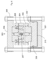
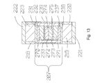
- the powder was placed in a foil cup 272, shown in Fig. 13 , and compressed to approximately to 30 kpsi [ ⁇ 207MPa] at room temperature to form an assembly of aluminium nitride 274 in the cup 272.
- a second assembly of aluminium nitride 275 in a cup 273 was prepared in like manner.
- the foil cups were made by pressing from tantalum foil, but niobium and other metals resistant to the temperatures required [typically above 2500°C] may substitute.
- cup 272 with aluminium nitride 274 and the second cup 273 with aluminium nitride 275 were placed mouth to mouth into a silicon carbide cylinder 233.
- a graphite disk 270 was placed over the cup 272 and a graphite disk 271 was placed under the cup 273.
- a disk of zirconia 232 was placed over the graphite disk 270.
- a disk of zirconia 237 was placed under the graphite disk 271.
- a zirconia disk 231 was placed over the zirconia disk 232 and a zirconia disk 238 was placed under the zirconia disk 237 closing the ends of the SiC cylinder 233.
- the hydraulic piston 302 was raised causing the anvil 214 [which was a tungsten carbide anvil] to compress the process chamber 207 to approximately 460 kpsi [ ⁇ 3.2GPa].
- the iron disks 221 and 222 expand due to the high pressure which seals the process chamber 207 from the atmosphere.
- the process chamber 207 was then heated to 2500-2800°C, causing the AlN 274 and 275 to melt. The pressure and temperature were held for approximately 30 minutes and the temperature slowly reduced at approximately 10° C per minute.
- Figs. 6-9 above are based on the premise that the cavity in which the process chamber and insulating liner are housed is frusto-conical in form and closed at the end remote from the punch or anvil by a tungsten carbide insert 212. While a frusto-conical form is the simplest shape to meet the requirements of the invention, it will be evident that other shapes in which the cavity narrows towards a mouth through which the punch extends are possible.
- the cavity may comprise two or more frusto-conical sections of different conical angle.
- the cavity may comprise two opposed cavities, and a punch or anvil may extend into a narrow mouth of each cavity.
- Fig. 16 shows crystallized AlN produced in the HPHT machine using the alleged high purity AlN powder.
- the crystals are quite small; however the starting AlN powder was subsequently found to have 3-5% oxygen contamination.
- Purchased AlN powder (advertised as 3 nines) processed in the machine of Figs. 6-7 always had very small crystals, ⁇ 1 micron, and the crystals were dark gray to black, indicating significant amounts of impurities, primarily oxygen which was measured using secondary ion mass spectrometry [SIMS] and found to be 3-5% in the AlN power (the manufacturer of the AlN powder does not include the oxygen in the 3 nines).
- SIMS secondary ion mass spectrometry
- Fig. 16 does show that the present HTHP machine is capable of melting and re-crystallising AlN and with a suitably high purity source of AlN, large crystals may be obtained.
- a high purity source material can be the product of the PVD apparatus mentioned above.
Landscapes
- Chemical & Material Sciences (AREA)
- Engineering & Computer Science (AREA)
- Metallurgy (AREA)
- Organic Chemistry (AREA)
- Materials Engineering (AREA)
- Mechanical Engineering (AREA)
- Analytical Chemistry (AREA)
- Chemical Kinetics & Catalysis (AREA)
- Crystallography & Structural Chemistry (AREA)
- Combustion & Propulsion (AREA)
- Computer Hardware Design (AREA)
- Power Engineering (AREA)
- Condensed Matter Physics & Semiconductors (AREA)
- General Physics & Mathematics (AREA)
- Manufacturing & Machinery (AREA)
- Physics & Mathematics (AREA)
- Microelectronics & Electronic Packaging (AREA)
- Inorganic Chemistry (AREA)
- General Engineering & Computer Science (AREA)
- Crystals, And After-Treatments Of Crystals (AREA)
- Physical Vapour Deposition (AREA)
- Manufacture Of Porous Articles, And Recovery And Treatment Of Waste Products (AREA)
- Compositions Of Macromolecular Compounds (AREA)
- Manufacture Of Macromolecular Shaped Articles (AREA)
- Press Drives And Press Lines (AREA)
Applications Claiming Priority (2)
| Application Number | Priority Date | Filing Date | Title |
|---|---|---|---|
| US201161540558P | 2011-09-29 | 2011-09-29 | |
| EP12770084.7A EP2761642B1 (en) | 2011-09-29 | 2012-09-27 | Ion beam generator and method of manufacturing a composition using said generator |
Related Parent Applications (2)
| Application Number | Title | Priority Date | Filing Date |
|---|---|---|---|
| EP12770084.7A Division-Into EP2761642B1 (en) | 2011-09-29 | 2012-09-27 | Ion beam generator and method of manufacturing a composition using said generator |
| EP12770084.7A Division EP2761642B1 (en) | 2011-09-29 | 2012-09-27 | Ion beam generator and method of manufacturing a composition using said generator |
Publications (1)
| Publication Number | Publication Date |
|---|---|
| EP3012345A1 true EP3012345A1 (en) | 2016-04-27 |
Family
ID=47010546
Family Applications (2)
| Application Number | Title | Priority Date | Filing Date |
|---|---|---|---|
| EP12770084.7A Not-in-force EP2761642B1 (en) | 2011-09-29 | 2012-09-27 | Ion beam generator and method of manufacturing a composition using said generator |
| EP15175725.9A Withdrawn EP3012345A1 (en) | 2011-09-29 | 2012-09-27 | Inorganic materials, methods and apparatus for making same, and uses thereof |
Family Applications Before (1)
| Application Number | Title | Priority Date | Filing Date |
|---|---|---|---|
| EP12770084.7A Not-in-force EP2761642B1 (en) | 2011-09-29 | 2012-09-27 | Ion beam generator and method of manufacturing a composition using said generator |
Country Status (8)
| Country | Link |
|---|---|
| US (1) | US20140227527A1 (zh) |
| EP (2) | EP2761642B1 (zh) |
| JP (1) | JP2015501372A (zh) |
| KR (1) | KR20140082738A (zh) |
| CN (1) | CN104040675A (zh) |
| PL (1) | PL2761642T3 (zh) |
| TW (1) | TW201327615A (zh) |
| WO (1) | WO2013045596A2 (zh) |
Cited By (1)
| Publication number | Priority date | Publication date | Assignee | Title |
|---|---|---|---|---|
| US11572275B2 (en) | 2016-03-08 | 2023-02-07 | Shibaura Institute Of Technology | Aluminum nitride film, method of manufacturing aluminum nitride film, and high withstand voltage component |
Families Citing this family (18)
| Publication number | Priority date | Publication date | Assignee | Title |
|---|---|---|---|---|
| GB201300133D0 (en) | 2012-10-25 | 2013-02-20 | Morgan Crucible Co | Laminated materials, methods and apparatus for making same, and uses thereof |
| US9856577B2 (en) | 2013-09-04 | 2018-01-02 | Nitride Solutions, Inc. | Bulk diffusion crystal growth of nitride crystal |
| US9422621B2 (en) * | 2013-10-30 | 2016-08-23 | Skyworks Solutions, Inc. | Refractory metal barrier in semiconductor devices |
| KR101585889B1 (ko) * | 2014-02-27 | 2016-02-02 | 한국과학기술원 | 고효율 할로우 음극과 이를 적용한 음극 시스템 |
| US9571061B2 (en) * | 2014-06-06 | 2017-02-14 | Akoustis, Inc. | Integrated circuit configured with two or more single crystal acoustic resonator devices |
| US9537465B1 (en) * | 2014-06-06 | 2017-01-03 | Akoustis, Inc. | Acoustic resonator device with single crystal piezo material and capacitor on a bulk substrate |
| TWI559355B (zh) * | 2014-12-23 | 2016-11-21 | 漢辰科技股份有限公司 | 離子源 |
| DE102015101966B4 (de) * | 2015-02-11 | 2021-07-08 | Infineon Technologies Austria Ag | Verfahren zum Herstellen eines Halbleiterbauelements mit Schottkykontakt und Halbleiterbauelement |
| CN104822219B (zh) * | 2015-05-18 | 2017-09-19 | 京东方科技集团股份有限公司 | 等离子发生器、退火设备、镀膜结晶化设备及退火工艺 |
| KR101680258B1 (ko) * | 2015-08-10 | 2016-11-29 | 한국에너지기술연구원 | 전자빔 증발증착 장치용 도가니 |
| US11056532B2 (en) | 2016-07-01 | 2021-07-06 | Intel Corporation | Techniques for monolithic co-integration of polycrystalline thin-film bulk acoustic resonator devices and monocrystalline III-N semiconductor transistor devices |
| EP3318351B1 (de) * | 2016-11-02 | 2020-12-30 | Linde GmbH | Verfahren zur generativen fertigung eines 3-dimensionalen bauteils |
| FR3065330B1 (fr) * | 2017-04-13 | 2019-05-03 | Tyco Electronics France Sas | Outil pour souder un conducteur electrique avec un dispositif de connexion |
| JP2019189479A (ja) * | 2018-04-19 | 2019-10-31 | パナソニック株式会社 | Iii族窒化物結晶の製造方法 |
| TWI780167B (zh) * | 2018-06-26 | 2022-10-11 | 晶元光電股份有限公司 | 半導體基底以及半導體元件 |
| JP2020026078A (ja) * | 2018-08-10 | 2020-02-20 | 株式会社ミマキエンジニアリング | 転写方法 |
| US20220162741A1 (en) * | 2020-01-28 | 2022-05-26 | Ulvac, Inc. | Evaporator and deposition apparatus |
| CN113428830A (zh) * | 2021-05-26 | 2021-09-24 | 上海晶维材料科技有限公司 | 一种低激活温度高性能吸气薄膜 |
Citations (35)
| Publication number | Priority date | Publication date | Assignee | Title |
|---|---|---|---|---|
| US2918699A (en) | 1958-04-28 | 1959-12-29 | Research Corp | High pressure press |
| US2947610A (en) | 1958-01-06 | 1960-08-02 | Gen Electric | Method of making diamonds |
| GB1003845A (en) * | 1962-05-03 | 1965-09-08 | G V Planer Ltd | Improvements in or relating to heating by means of electron beams |
| US3440687A (en) | 1967-02-16 | 1969-04-29 | Howard T Hall | Multianvil press |
| GB1175920A (en) * | 1967-12-15 | 1970-01-01 | Matsushita Electric Ind Co Ltd | Improvements in or relating to Ceramic Coatings |
| JPS60200982A (ja) * | 1984-03-26 | 1985-10-11 | Tanaka Kikinzoku Kogyo Kk | クラツド容器 |
| US4618592A (en) | 1982-09-17 | 1986-10-21 | Tokuyama Soda Kabushiki Kaisha | Fine powder of aluminum nitride, composition and sintered body thereof and processes for their production |
| JPS62164870A (ja) * | 1986-01-13 | 1987-07-21 | Sumitomo Electric Ind Ltd | アルミニウム蒸着用るつぼ |
| JPS6395103A (ja) | 1986-10-03 | 1988-04-26 | Nec Corp | 易焼結性窒化アルミニウム粉末及びその製造方法 |
| US4997673A (en) | 1987-09-10 | 1991-03-05 | Nissin Electric Co., Ltd. | Method of forming aluminum nitride films by ion-assisted evaporation |
| US5534314A (en) | 1994-08-31 | 1996-07-09 | University Of Virginia Patent Foundation | Directed vapor deposition of electron beam evaporant |
| US5744170A (en) | 1994-03-14 | 1998-04-28 | Hall; H. Tracy | Guided high pressure presses |
| US5858086A (en) | 1996-10-17 | 1999-01-12 | Hunter; Charles Eric | Growth of bulk single crystals of aluminum nitride |
| US5954874A (en) | 1996-10-17 | 1999-09-21 | Hunter; Charles Eric | Growth of bulk single crystals of aluminum nitride from a melt |
| US5993699A (en) | 1997-06-06 | 1999-11-30 | Ngk Insulators, Ltd. | Aluminum nitride based composite body electronic functional material, electrostatic chuck and method of producing aluminum nitride based composite body |
| DE10111515A1 (de) * | 2001-02-19 | 2002-08-14 | Fraunhofer Ges Forschung | Plasma-Beschichtungsanlage, Plasma-Beschichtungsverfahren und Verwendung des Verfahrens |
| US6596079B1 (en) | 2000-03-13 | 2003-07-22 | Advanced Technology Materials, Inc. | III-V nitride substrate boule and method of making and using the same |
| US6616757B1 (en) | 2001-07-06 | 2003-09-09 | Technologies And Devices International, Inc. | Method for achieving low defect density GaN single crystal boules |
| US6692568B2 (en) | 2000-11-30 | 2004-02-17 | Kyma Technologies, Inc. | Method and apparatus for producing MIIIN columns and MIIIN materials grown thereon |
| US6936357B2 (en) | 2001-07-06 | 2005-08-30 | Technologies And Devices International, Inc. | Bulk GaN and ALGaN single crystals |
| US20050229856A1 (en) * | 2004-04-20 | 2005-10-20 | Malik Roger J | Means and method for a liquid metal evaporation source with integral level sensor and external reservoir |
| JP2005330146A (ja) * | 2004-05-19 | 2005-12-02 | Hitachi Chem Co Ltd | フッ化カルシウム結晶育成ルツボ、フッ化カルシウム結晶の製造方法及びフッ化カルシウム結晶 |
| US7056383B2 (en) | 2004-02-13 | 2006-06-06 | The Fox Group, Inc. | Tantalum based crucible |
| US7075111B2 (en) | 2003-11-14 | 2006-07-11 | Hitachi Cable, Ltd. | Nitride semiconductor substrate and its production method |
| US20060280668A1 (en) | 2001-07-06 | 2006-12-14 | Technologies And Devices International, Inc. | Method and apparatus for fabricating crack-free group III nitride semiconductor materials |
| EP1743961A1 (en) | 2004-03-19 | 2007-01-17 | Nippon Mining & Metals Co., Ltd. | Compound semiconductor substrate |
| US20070101932A1 (en) | 2001-12-24 | 2007-05-10 | Crystal Is, Inc. | Method and apparatus for producing large, single-crystals of aluminum nitride |
| WO2007062250A2 (en) | 2005-11-28 | 2007-05-31 | Crystal Is, Inc. | Large aluminum nitride crystals with reduced defects and methods of making them |
| US20070169689A1 (en) | 2006-01-10 | 2007-07-26 | Ngk Insulators, Ltd. | Manufacturing method of aluminum nitride single crystal and aluminum nitride single crystal |
| US7294198B2 (en) | 2003-07-29 | 2007-11-13 | Japan Atomic Energy Research Institute | Process for producing single-crystal gallium nitride |
| US7494546B1 (en) | 2006-07-14 | 2009-02-24 | Blue Wave Semicodnuctors, Inc. | Method of growing insulating, semiconducting, and conducting group III-nitride thin films and coatings, and use as radiation hard coatings for electronics and optoelectronic devices |
| WO2009066286A2 (en) | 2007-11-20 | 2009-05-28 | Mosaic Crystals Ltd. | Amorphous group iii-v semiconductor material and preparation thereof |
| WO2009092097A1 (en) | 2008-01-18 | 2009-07-23 | 4D-S Pty Ltd. | Concentric hollow cathode magnetron sputter source |
| US7576372B2 (en) | 2001-08-01 | 2009-08-18 | Crystal Photonics, Incorporated | Method for making free-standing AlGaN wafer, wafer produced thereby, and associated methods and devices using the wafer |
| US7642122B2 (en) | 2006-10-08 | 2010-01-05 | Momentive Performance Materials Inc. | Method for forming nitride crystals |
Family Cites Families (13)
| Publication number | Priority date | Publication date | Assignee | Title |
|---|---|---|---|---|
| US5317006A (en) * | 1989-06-15 | 1994-05-31 | Microelectronics And Computer Technology Corporation | Cylindrical magnetron sputtering system |
| JPH05230654A (ja) * | 1992-02-24 | 1993-09-07 | Nkk Corp | 合金皮膜のイオンプレーティング方法および装置 |
| US5227203A (en) * | 1992-02-24 | 1993-07-13 | Nkk Corporation | Ion-plating method and apparatus therefor |
| US6958093B2 (en) * | 1994-01-27 | 2005-10-25 | Cree, Inc. | Free-standing (Al, Ga, In)N and parting method for forming same |
| DE4412906C1 (de) * | 1994-04-14 | 1995-07-13 | Fraunhofer Ges Forschung | Verfahren und Einrichtung für die ionengestützte Vakuumbeschichtung |
| US5886863A (en) * | 1995-05-09 | 1999-03-23 | Kyocera Corporation | Wafer support member |
| DE19841012C1 (de) * | 1998-09-08 | 2000-01-13 | Fraunhofer Ges Forschung | Einrichtung zum plasmaaktivierten Bedampfen im Vakuum |
| US6949395B2 (en) * | 2001-10-22 | 2005-09-27 | Oriol, Inc. | Method of making diode having reflective layer |
| US20050025973A1 (en) * | 2003-07-25 | 2005-02-03 | Slutz David E. | CVD diamond-coated composite substrate containing a carbide-forming material and ceramic phases and method for making same |
| EP2573206B1 (en) * | 2004-09-27 | 2014-06-11 | Gallium Enterprises Pty Ltd | Method for growing a group (iii) metal nitride film |
| JP2009536605A (ja) * | 2006-05-08 | 2009-10-15 | ザ リージェンツ オブ ザ ユニバーシティ オブ カリフォルニア | アルミニウムを含むiii族窒化物半導体化合物の成長方法及び材料。 |
| RU2389832C1 (ru) * | 2008-10-14 | 2010-05-20 | Общество с ограниченной ответственностью "Аккорд" | ТИГЕЛЬ ДЛЯ ВЫРАЩИВАНИЯ ОБЪЕМНОГО МОНОКРИСТАЛЛА НИТРИДА АЛЮМИНИЯ (AlN) |
| DE102008064134B4 (de) * | 2008-12-19 | 2016-07-21 | Fraunhofer-Gesellschaft zur Förderung der angewandten Forschung e.V. | Verfahren zur Beschichtung von Gegenständen mittels eines Niederdruckplasmas |
-
2012
- 2012-09-27 EP EP12770084.7A patent/EP2761642B1/en not_active Not-in-force
- 2012-09-27 PL PL12770084T patent/PL2761642T3/pl unknown
- 2012-09-27 US US14/348,406 patent/US20140227527A1/en not_active Abandoned
- 2012-09-27 JP JP2014532397A patent/JP2015501372A/ja active Pending
- 2012-09-27 EP EP15175725.9A patent/EP3012345A1/en not_active Withdrawn
- 2012-09-27 KR KR20147011121A patent/KR20140082738A/ko not_active Application Discontinuation
- 2012-09-27 WO PCT/EP2012/069156 patent/WO2013045596A2/en active Application Filing
- 2012-09-27 CN CN201280058733.XA patent/CN104040675A/zh active Pending
- 2012-09-28 TW TW101136101A patent/TW201327615A/zh unknown
Patent Citations (41)
| Publication number | Priority date | Publication date | Assignee | Title |
|---|---|---|---|---|
| US2947610A (en) | 1958-01-06 | 1960-08-02 | Gen Electric | Method of making diamonds |
| US2918699A (en) | 1958-04-28 | 1959-12-29 | Research Corp | High pressure press |
| GB1003845A (en) * | 1962-05-03 | 1965-09-08 | G V Planer Ltd | Improvements in or relating to heating by means of electron beams |
| US3440687A (en) | 1967-02-16 | 1969-04-29 | Howard T Hall | Multianvil press |
| GB1175920A (en) * | 1967-12-15 | 1970-01-01 | Matsushita Electric Ind Co Ltd | Improvements in or relating to Ceramic Coatings |
| US4618592A (en) | 1982-09-17 | 1986-10-21 | Tokuyama Soda Kabushiki Kaisha | Fine powder of aluminum nitride, composition and sintered body thereof and processes for their production |
| JPS60200982A (ja) * | 1984-03-26 | 1985-10-11 | Tanaka Kikinzoku Kogyo Kk | クラツド容器 |
| JPS62164870A (ja) * | 1986-01-13 | 1987-07-21 | Sumitomo Electric Ind Ltd | アルミニウム蒸着用るつぼ |
| JPS6395103A (ja) | 1986-10-03 | 1988-04-26 | Nec Corp | 易焼結性窒化アルミニウム粉末及びその製造方法 |
| US4997673A (en) | 1987-09-10 | 1991-03-05 | Nissin Electric Co., Ltd. | Method of forming aluminum nitride films by ion-assisted evaporation |
| US5744170A (en) | 1994-03-14 | 1998-04-28 | Hall; H. Tracy | Guided high pressure presses |
| US5534314A (en) | 1994-08-31 | 1996-07-09 | University Of Virginia Patent Foundation | Directed vapor deposition of electron beam evaporant |
| US5858086A (en) | 1996-10-17 | 1999-01-12 | Hunter; Charles Eric | Growth of bulk single crystals of aluminum nitride |
| US5954874A (en) | 1996-10-17 | 1999-09-21 | Hunter; Charles Eric | Growth of bulk single crystals of aluminum nitride from a melt |
| US5972109A (en) | 1996-10-17 | 1999-10-26 | Hunter; Charles Eric | Growth of bulk single crystals of aluminum nitride |
| US6066205A (en) | 1996-10-17 | 2000-05-23 | Cree, Inc. | Growth of bulk single crystals of aluminum nitride from a melt |
| US6296956B1 (en) | 1996-10-17 | 2001-10-02 | Cree, Inc. | Bulk single crystals of aluminum nitride |
| US5993699A (en) | 1997-06-06 | 1999-11-30 | Ngk Insulators, Ltd. | Aluminum nitride based composite body electronic functional material, electrostatic chuck and method of producing aluminum nitride based composite body |
| US6596079B1 (en) | 2000-03-13 | 2003-07-22 | Advanced Technology Materials, Inc. | III-V nitride substrate boule and method of making and using the same |
| US7655197B2 (en) | 2000-03-13 | 2010-02-02 | Cree, Inc. | III-V nitride substrate boule and method of making and using the same |
| US6692568B2 (en) | 2000-11-30 | 2004-02-17 | Kyma Technologies, Inc. | Method and apparatus for producing MIIIN columns and MIIIN materials grown thereon |
| US6784085B2 (en) | 2000-11-30 | 2004-08-31 | North Carolina State University | MIIIN based materials and methods and apparatus for producing same |
| DE10111515A1 (de) * | 2001-02-19 | 2002-08-14 | Fraunhofer Ges Forschung | Plasma-Beschichtungsanlage, Plasma-Beschichtungsverfahren und Verwendung des Verfahrens |
| US6616757B1 (en) | 2001-07-06 | 2003-09-09 | Technologies And Devices International, Inc. | Method for achieving low defect density GaN single crystal boules |
| US20060280668A1 (en) | 2001-07-06 | 2006-12-14 | Technologies And Devices International, Inc. | Method and apparatus for fabricating crack-free group III nitride semiconductor materials |
| US6936357B2 (en) | 2001-07-06 | 2005-08-30 | Technologies And Devices International, Inc. | Bulk GaN and ALGaN single crystals |
| US20090092815A1 (en) | 2001-07-06 | 2009-04-09 | Technologies And Devices International, Inc. | Method and apparatus for fabricating crack-free group iii nitride semiconductor materials |
| US7576372B2 (en) | 2001-08-01 | 2009-08-18 | Crystal Photonics, Incorporated | Method for making free-standing AlGaN wafer, wafer produced thereby, and associated methods and devices using the wafer |
| US20070101932A1 (en) | 2001-12-24 | 2007-05-10 | Crystal Is, Inc. | Method and apparatus for producing large, single-crystals of aluminum nitride |
| US7294198B2 (en) | 2003-07-29 | 2007-11-13 | Japan Atomic Energy Research Institute | Process for producing single-crystal gallium nitride |
| US7075111B2 (en) | 2003-11-14 | 2006-07-11 | Hitachi Cable, Ltd. | Nitride semiconductor substrate and its production method |
| US7056383B2 (en) | 2004-02-13 | 2006-06-06 | The Fox Group, Inc. | Tantalum based crucible |
| EP1743961A1 (en) | 2004-03-19 | 2007-01-17 | Nippon Mining & Metals Co., Ltd. | Compound semiconductor substrate |
| US20050229856A1 (en) * | 2004-04-20 | 2005-10-20 | Malik Roger J | Means and method for a liquid metal evaporation source with integral level sensor and external reservoir |
| JP2005330146A (ja) * | 2004-05-19 | 2005-12-02 | Hitachi Chem Co Ltd | フッ化カルシウム結晶育成ルツボ、フッ化カルシウム結晶の製造方法及びフッ化カルシウム結晶 |
| WO2007062250A2 (en) | 2005-11-28 | 2007-05-31 | Crystal Is, Inc. | Large aluminum nitride crystals with reduced defects and methods of making them |
| US20070169689A1 (en) | 2006-01-10 | 2007-07-26 | Ngk Insulators, Ltd. | Manufacturing method of aluminum nitride single crystal and aluminum nitride single crystal |
| US7494546B1 (en) | 2006-07-14 | 2009-02-24 | Blue Wave Semicodnuctors, Inc. | Method of growing insulating, semiconducting, and conducting group III-nitride thin films and coatings, and use as radiation hard coatings for electronics and optoelectronic devices |
| US7642122B2 (en) | 2006-10-08 | 2010-01-05 | Momentive Performance Materials Inc. | Method for forming nitride crystals |
| WO2009066286A2 (en) | 2007-11-20 | 2009-05-28 | Mosaic Crystals Ltd. | Amorphous group iii-v semiconductor material and preparation thereof |
| WO2009092097A1 (en) | 2008-01-18 | 2009-07-23 | 4D-S Pty Ltd. | Concentric hollow cathode magnetron sputter source |
Non-Patent Citations (1)
| Title |
|---|
| ROMAN Y G ET AL: "Aluminium nitride films made by low pressure chemical vapour deposition: Preparation and properties", THIN SOLID FILMS, ELSEVIER-SEQUOIA S.A. LAUSANNE, CH, vol. 169, no. 2, 15 February 1989 (1989-02-15), pages 241 - 248, XP025852262, ISSN: 0040-6090, [retrieved on 19890215], DOI: 10.1016/0040-6090(89)90707-4 * |
Cited By (1)
| Publication number | Priority date | Publication date | Assignee | Title |
|---|---|---|---|---|
| US11572275B2 (en) | 2016-03-08 | 2023-02-07 | Shibaura Institute Of Technology | Aluminum nitride film, method of manufacturing aluminum nitride film, and high withstand voltage component |
Also Published As
| Publication number | Publication date |
|---|---|
| PL2761642T3 (pl) | 2018-03-30 |
| EP2761642B1 (en) | 2017-08-23 |
| TW201327615A (zh) | 2013-07-01 |
| KR20140082738A (ko) | 2014-07-02 |
| WO2013045596A3 (en) | 2013-08-08 |
| CN104040675A (zh) | 2014-09-10 |
| WO2013045596A2 (en) | 2013-04-04 |
| JP2015501372A (ja) | 2015-01-15 |
| EP2761642A2 (en) | 2014-08-06 |
| US20140227527A1 (en) | 2014-08-14 |
Similar Documents
| Publication | Publication Date | Title |
|---|---|---|
| EP2761642B1 (en) | Ion beam generator and method of manufacturing a composition using said generator | |
| TWI668198B (zh) | 氮化鎵系燒結體及其製造方法 | |
| US9711590B2 (en) | Semiconductor device, or crystal | |
| JP6667490B2 (ja) | 多結晶質窒化アルミニウム焼結体の熱膨張処理、および半導体製造へのその応用 | |
| US6784085B2 (en) | MIIIN based materials and methods and apparatus for producing same | |
| KR101935755B1 (ko) | 금속 갈륨 침투 질화갈륨 성형물 및 이의 제조방법 | |
| JP4979442B2 (ja) | Gaスパッタターゲットの製造方法 | |
| JP2017024970A (ja) | 窒化ガリウム系焼結体及びその製造方法 | |
| KR20210071954A (ko) | 질화갈륨계 소결체 및 그 제조 방법 | |
| JP7500941B2 (ja) | 窒化ガリウム系焼結体及びその製造方法 | |
| Guo et al. | Growth condition dependence of structure and surface morphology of GaN films on (111) GaAs substrates prepared by reactive sputtering | |
| JP2024040414A (ja) | 窒化ガリウム系焼結体及びその製造方法 | |
| JP6446681B2 (ja) | 積層構造体の製造方法 |
Legal Events
| Date | Code | Title | Description |
|---|---|---|---|
| PUAI | Public reference made under article 153(3) epc to a published international application that has entered the european phase |
Free format text: ORIGINAL CODE: 0009012 |
|
| 17P | Request for examination filed |
Effective date: 20150728 |
|
| AC | Divisional application: reference to earlier application |
Ref document number: 2761642 Country of ref document: EP Kind code of ref document: P |
|
| AK | Designated contracting states |
Kind code of ref document: A1 Designated state(s): AL AT BE BG CH CY CZ DE DK EE ES FI FR GB GR HR HU IE IS IT LI LT LU LV MC MK MT NL NO PL PT RO RS SE SI SK SM TR |
|
| RIN1 | Information on inventor provided before grant (corrected) |
Inventor name: SLUTZ, DAVID Inventor name: DEMARAY, RICHARD Inventor name: BRORS, DANIEL |
|
| STAA | Information on the status of an ep patent application or granted ep patent |
Free format text: STATUS: THE APPLICATION IS DEEMED TO BE WITHDRAWN |
|
| 18D | Application deemed to be withdrawn |
Effective date: 20161028 |