EP2997433B1 - On-chip versorgungsgenerator mit dynamischer schaltungsreferenz - Google Patents
On-chip versorgungsgenerator mit dynamischer schaltungsreferenz Download PDFInfo
- Publication number
- EP2997433B1 EP2997433B1 EP13884830.4A EP13884830A EP2997433B1 EP 2997433 B1 EP2997433 B1 EP 2997433B1 EP 13884830 A EP13884830 A EP 13884830A EP 2997433 B1 EP2997433 B1 EP 2997433B1
- Authority
- EP
- European Patent Office
- Prior art keywords
- power supply
- voltage
- adc
- sensing block
- receive
- Prior art date
- Legal status (The legal status is an assumption and is not a legal conclusion. Google has not performed a legal analysis and makes no representation as to the accuracy of the status listed.)
- Active
Links
Images


Classifications
-
- G—PHYSICS
- G05—CONTROLLING; REGULATING
- G05F—SYSTEMS FOR REGULATING ELECTRIC OR MAGNETIC VARIABLES
- G05F1/00—Automatic systems in which deviations of an electric quantity from one or more predetermined values are detected at the output of the system and fed back to a device within the system to restore the detected quantity to its predetermined value or values, i.e. retroactive systems
- G05F1/10—Regulating voltage or current
- G05F1/46—Regulating voltage or current wherein the variable actually regulated by the final control device is DC
- G05F1/56—Regulating voltage or current wherein the variable actually regulated by the final control device is DC using semiconductor devices in series with the load as final control devices
-
- G—PHYSICS
- G01—MEASURING; TESTING
- G01K—MEASURING TEMPERATURE; MEASURING QUANTITY OF HEAT; THERMALLY-SENSITIVE ELEMENTS NOT OTHERWISE PROVIDED FOR
- G01K7/00—Measuring temperature based on the use of electric or magnetic elements directly sensitive to heat ; Power supply therefor, e.g. using thermoelectric elements
-
- G—PHYSICS
- G01—MEASURING; TESTING
- G01K—MEASURING TEMPERATURE; MEASURING QUANTITY OF HEAT; THERMALLY-SENSITIVE ELEMENTS NOT OTHERWISE PROVIDED FOR
- G01K7/00—Measuring temperature based on the use of electric or magnetic elements directly sensitive to heat ; Power supply therefor, e.g. using thermoelectric elements
- G01K7/01—Measuring temperature based on the use of electric or magnetic elements directly sensitive to heat ; Power supply therefor, e.g. using thermoelectric elements using semiconducting elements having PN junctions
-
- G—PHYSICS
- G05—CONTROLLING; REGULATING
- G05F—SYSTEMS FOR REGULATING ELECTRIC OR MAGNETIC VARIABLES
- G05F1/00—Automatic systems in which deviations of an electric quantity from one or more predetermined values are detected at the output of the system and fed back to a device within the system to restore the detected quantity to its predetermined value or values, i.e. retroactive systems
- G05F1/10—Regulating voltage or current
- G05F1/46—Regulating voltage or current wherein the variable actually regulated by the final control device is DC
- G05F1/56—Regulating voltage or current wherein the variable actually regulated by the final control device is DC using semiconductor devices in series with the load as final control devices
- G05F1/565—Regulating voltage or current wherein the variable actually regulated by the final control device is DC using semiconductor devices in series with the load as final control devices sensing a condition of the system or its load in addition to means responsive to deviations in the output of the system, e.g. current, voltage, power factor
- G05F1/567—Regulating voltage or current wherein the variable actually regulated by the final control device is DC using semiconductor devices in series with the load as final control devices sensing a condition of the system or its load in addition to means responsive to deviations in the output of the system, e.g. current, voltage, power factor for temperature compensation
-
- G—PHYSICS
- G06—COMPUTING OR CALCULATING; COUNTING
- G06F—ELECTRIC DIGITAL DATA PROCESSING
- G06F1/00—Details not covered by groups G06F3/00 - G06F13/00 and G06F21/00
- G06F1/26—Power supply means, e.g. regulation thereof
-
- H—ELECTRICITY
- H02—GENERATION; CONVERSION OR DISTRIBUTION OF ELECTRIC POWER
- H02M—APPARATUS FOR CONVERSION BETWEEN AC AND AC, BETWEEN AC AND DC, OR BETWEEN DC AND DC, AND FOR USE WITH MAINS OR SIMILAR POWER SUPPLY SYSTEMS; CONVERSION OF DC OR AC INPUT POWER INTO SURGE OUTPUT POWER; CONTROL OR REGULATION THEREOF
- H02M3/00—Conversion of DC power input into DC power output
- H02M3/02—Conversion of DC power input into DC power output without intermediate conversion into AC
- H02M3/04—Conversion of DC power input into DC power output without intermediate conversion into AC by static converters
- H02M3/06—Conversion of DC power input into DC power output without intermediate conversion into AC by static converters using resistors or capacitors, e.g. potential divider
- H02M3/07—Conversion of DC power input into DC power output without intermediate conversion into AC by static converters using resistors or capacitors, e.g. potential divider using capacitors charged and discharged alternately by semiconductor devices with control electrode, e.g. charge pumps
-
- G—PHYSICS
- G01—MEASURING; TESTING
- G01K—MEASURING TEMPERATURE; MEASURING QUANTITY OF HEAT; THERMALLY-SENSITIVE ELEMENTS NOT OTHERWISE PROVIDED FOR
- G01K2215/00—Details concerning sensor power supply
-
- G—PHYSICS
- G05—CONTROLLING; REGULATING
- G05F—SYSTEMS FOR REGULATING ELECTRIC OR MAGNETIC VARIABLES
- G05F1/00—Automatic systems in which deviations of an electric quantity from one or more predetermined values are detected at the output of the system and fed back to a device within the system to restore the detected quantity to its predetermined value or values, i.e. retroactive systems
- G05F1/10—Regulating voltage or current
- G05F1/46—Regulating voltage or current wherein the variable actually regulated by the final control device is DC
- G05F1/468—Regulating voltage or current wherein the variable actually regulated by the final control device is DC characterised by reference voltage circuitry, e.g. soft start, remote shutdown
Definitions
- Some analog circuits require more than one supply input. Usually, in addition to the digital supply (e.g., mostly 1.0V), an additional higher supply is required. An example of that is a thermal sensor circuit, which may require a 1.25V analog supply, in addition to the 1.0V digital supply. As the trend for SoC (system-on-chip) or processor chip to reduce the number of analog circuits is becoming popular, fewer analog voltage supplies are available. Performance of analog circuits depends on a quiet analog power supply. One way to provide a quiet analog power supply for an analog circuit is to provide a dedicated supply bump for that analog circuit i.e., each analog circuit may have its own dedicated source of analog power supply. Providing an external supply bump for every single analog component is very expensive.
- Document EP 0 500 381 A2 discloses an adaptive voltage regulator.
- a regulated power supply provides a regulated supply voltage at a preselected level under normal operating conditions. When power demands of the circuitry driven by the supply requires a higher voltage, the supply adapts to supply such a higher voltage.
- Such a supply can be used with automotive electronic circuitry, and can supply voltages up to approximately the voltage available on an automobile battery.
- Document US 8,290,171 B1 discloses an integrated circuit device including a charge pump, a multi-voltage LDO and an analog to digital converter.
- US 2009/015299 A1 discloses a reference voltage is applied from a reference voltage generating circuit to the non-inverting input terminal of an amplifier for supplying a drive voltage to the gate terminal of an NMOS transistor, and the output voltage appearing at the source terminal of the NMOS transistor is divided by a resistor pair and applied to the inverting input terminal of the amplifier.
- the voltage obtained by adding a voltage equal to or higher than the voltage for sufficiently driving the NMOS transistor to the output voltage appearing at the source terminal of the NMOS transistor is generated by a charge pump circuit and supplied to the amplifier as a power supply voltage.
- US 6,847,319 B1 discloses a temperature to digital converter device is implemented by integrating a temperature sensor circuit into an analog-to-digital converter (ADC). Temperature-to-digital conversion is accomplished by first measuring a change in voltage (DeltaVBE) across the junction of a diode when different current densities are forced through the junction. The thus obtained DeltaVBE is proportional to temperature. As part of the conversion processing, DeltaVBE is multiplied by a fixed gain, and an offset voltage value is subtracted from DeltaVBE.
- ADC analog-to-digital converter
- the multiplication and subtraction functions are performed by a switched-capacitor integrator in a delta-sigma ADC and the ADC itself operates as the temperature-to-digital converter device, eliminating the extra amplifier and/or capacitors required when the multiplication and/or subtraction function are performed outside the ADC.; Alternately, other ADC topologies that include an integrator or gain amplifier, such as pipeline ADCs and cyclic ADCs may be used in place of the delta-sigma ADC.
- the embodiments describe an apparatus which generates analog voltage, using a digital supply, with relatively high power efficiency.
- One technical effect of the embodiments is that it reduces or eliminates the need for an analog supply bump.
- a dynamic, self-calibrated bandgap circuit is used to obtain the accuracy in the supplied analog voltage.
- the embodiments describe a power supply generator using dynamic reference to adjust power supply for a load.
- a digital power supply (e.g., 1V, also referred here as the first power supply) is received by a charge pump which generates a higher power supply (e.g., 2.0V, also referred here as the second power supply) which is then regulated by a voltage regulator that generates a regulated analog power supply (e.g., 1.25V, also referred here as the third power supply).
- the regulated analog power supply is provided to a voltage sensing block and to a load (e.g., thermal sensor, phase locked loop (PLL), analog-to-digital converter (ADC), etc.).
- a reference voltage for the voltage regulator is adjusted dynamically according to changing conditions of the voltage sensing block and/or the load.
- a thermal sensor is used as a voltage sensing block coupled in parallel to the load.
- other analog circuits may be used as the voltage sensing block.
- an ADC may be used as a voltage sensing block.
- a dynamic self-calibrated bandgap circuit is used to obtain a highly accurate (e.g., less than 3% variation across process, voltage, and temperature variations) analog power supply without the use of a dedicated analog supply bump.
- the power supply generator is fully integrated with the circuits of the voltage sensing block to form a feedback circuit that regulates the power supply while allowing the voltage sensing block to function for its purpose.
- the power supply generator is based on a switch capacitor charge pump integrated with a thermal sensor sigma-delta analog-to-digital converter (SD-ADC) with dynamic bandgap reference to provide an accurate analog power supply for the thermal sensor (i.e., voltage sensing block).
- SD-ADC samples its own power supply (i.e., third power supply) with a dynamic bandgap voltage supplied by the thermal sensor's sense stage.
- signals are represented with lines. Some lines may be thicker, to indicate more constituent signal paths, and/or have arrows at one or more ends, to indicate primary information flow direction. Such indications are not intended to be limiting. Rather, the lines are used in connection with one or more exemplary embodiments to facilitate easier understanding of a circuit or a logical unit. Any represented signal, as dictated by design needs or preferences, may actually comprise one or more signals that may travel in either direction and may be implemented with any suitable type of signal scheme.
- connection means a direct electrical connection between the things that are connected, without any intermediary devices.
- coupled means either a direct electrical connection between the things that are connected or an indirect connection through one or more passive or active intermediary devices.
- circuit means one or more passive and/or active components that are arranged to cooperate with one another to provide a desired function.
- signal means at least one current signal, voltage signal or data/clock signal.
- scaling generally refers to converting a design (schematic and layout) from one process technology to another process technology.
- scaling generally also refers to downsizing layout and devices within the same technology node.
- scaling may also refer to adjusting (e.g., slow down) of a signal frequency relative to another parameter, for example, power supply level.
- substantially generally refer to being within +/- 20% of a target value.
- the transistors are metal oxide semiconductor (MOS) transistors, which include drain, source, gate, and bulk terminals.
- MOS metal oxide semiconductor
- the transistors also include Tri-Gate and FinFet transistors, Gate All Around Cylindrical Transistors or other devices implementing transistor functionality like carbon nano tubes or spintronic devices.
- Source and drain terminals may be identical terminals and are interchangeably used herein.
- transistors for example, Bi-polar junction transistors-BJT PNP/NPN, BiCMOS, CMOS, eFET, etc., may be used without departing from the scope of the disclosure.
- MN indicates an n-type transistor (e.g., NMOS, NPN BJT, etc.) and the term “MP” indicates a p-type transistor (e.g., PMOS, PNP BJT, etc.).
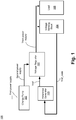
- Fig. 1 illustrates a high level architecture 100 of a power supply generator using dynamic reference, according to one embodiment of the disclosure.
- architecture 100 comprises a charge pump 101, voltage regulator 102, reference generator 103, and voltage sensing block 104 (e.g., thermal sensor, ADC, etc.), and load 105.
- voltage sensing block 104 e.g., thermal sensor, ADC, etc.
- charge pump 101 receives a first power supply and generates a higher second power supply using the first power supply.
- charge pump 101 receives a low digital power supply of 1V as the first power supply and pumps that first power supply using switch capacitors to generate a higher unregulated second power supply of 1.5V or 2.0V.
- An exemplary embodiment of charge pump 101 is described with reference to Fig. 3 .
- voltage regulator 102 receives the second power supply as input power supply and generates a regulated third power supply for voltage sensing block 104.
- voltage regulator 102 compares a reference voltage Vref with a divided down version of third power supply to regulate the third power supply.
- voltage regulator 102 is a low dropout (LDO) voltage regulator. In other embodiments, other types of voltage regulators may be used. An exemplary embodiment of voltage regulator 102 is described with reference to Fig. 4 .
- reference generator 103 provides Vref to voltage regulator 102 according to Vref_code.
- Vref_code is a digital code that adjusts resistance of a resistor (or transistor) of reference generator 103.
- Vref_code may be an analog signal to control resistance of a resistor (or transistor) of reference generator 103.
- Vref_code is adjusted by a SD-ADC (not shown) of the voltage sensing block 104 after sampling the third power supply with dynamic bandgap voltage.
- voltage sensing block 104 (which is mostly an analog circuit) receives an accurate third power supply and provides Vref_code for reference generator 103 to adjust Vref to regulate the third power supply.
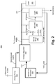
- Fig. 2 illustrates architecture 200 of power supply generator for a thermal sensor using dynamic reference, according to one embodiment of the disclosure. It is pointed out that those elements of Fig. 2 having the same reference numbers (or names) as the elements of any other figure can operate or function in any manner similar to that described, but are not limited to such.
- a thermal sensor 201 is used as voltage sensing block 104.
- voltage sensing block 201 comprises a sense stage 202, SD-ADC 203, logic 204, and sampling circuit with resistors Rs1 and Rs2.
- sense stage 202 comprises current sources and two sets of diodes.
- the first set of diode provides Vbel (i.e., base-emitter voltage) and the second set of diodes provides Vbe2.
- sense stage 202 operates using third power supply.
- the difference of Vbel and Vbe2 is used to determine temperature of the diodes of the sense stage 201.
- sampling circuit comprises a voltage divider having resistors Rs1 and Rs2 coupled together as shown to provide Vsample, which is a divided down voltage of third power supply.
- resistors Rs1 and Rs2 are of equal resistance values. In such an embodiment, Vsample is half of third power supply. In other embodiments other resistance ratios of resistors Rs1 and Rs2 may be used to adjust the level of Vsample.
- resistors Rs1 and Rs2 each are a number of parallel resistors that can be enabled or disabled.
- resistors Rs1 and Rs2 are implemented as transistors. In other embodiments, resistors Rs1 and Rs2 can be implemented as poly resistors or combination of transistors and poly resistors.
- SD-ADC 203 receives Vsample and samples it using Vbel and Vbe2.
- SD-ADC 203 includes a first order sigma-delta modulator.
- SD-ADC 203 includes a second order sigma-delta modulator. In other embodiments, higher order of SD-ADC 203 may be used.
- SD-ADC 203 is time-interleaved ADC.
- output of SD-ADC 203 is a bit stream which is received by logic 204.
- logic 204 is a digital filter.
- digital filter is one of finite impulse response (FIR) filter, infinite impulse response (IIR) filter, cascaded integrator-comb (CIC) low pass filter, etc.
- logic 204 comprises three stages of CIC low pass filter.
- the CIC filter configuration has configurable decimation ratio of 64 or 256.
- logic 204 generates a temperature reading (or measurement).
- logic 204 also generates Vref_code for adjusting Vref.
- logic 204 also generates phases for SD ADC 203.
- logic 204 also has a calibration FSM (finite state machine) to calibrate Vref and the third power supply.
- FSM finite state machine
- virtual Vbg (i.e., dynamic bandgap reference voltage) is created using dynamic sense stage 202.
- current drawn on the two sets of diodes and voltages Vbel and ⁇ Vbe i.e., Vbe2-Vbe1 are measured.
- Vbel (and Vbe2) are complementary to absolute temperature (CTAT), and ⁇ Vbe is proportional to absolute temperature (PTAT).
- virtual Vbg is expressed as Vbe+ ⁇ * ⁇ Vbe, where ⁇ is a constant multiplier (e.g., 16), and virtual Vbg is substantially constant with changes in temperature.
- the base-emitter voltage has a negative temperature coefficient, e.g., of about 2 mV/°C. The exact value depends on the absolute value of I s and I bias .
- the extrapolated value of Vbe to OK is related to the silicon bandgap energy. This voltage is independent of the absolute values of and I s and I bias .
- bandgap reference can be used as the reference voltage of SD-ADC 203.
- virtual Vbg (or dynamic reference voltage) is generated by adding an amplified version of ⁇ Vbe to Vbe to obtain a temperature-independent voltage virtual Vbg.
- Fig. 3 illustrates a charge pump 300 for the power supply generator, according to one embodiment of the disclosure. It is pointed out that those elements of Fig. 3 having the same reference numbers (or names) as the elements of any other figure can operate or function in any manner similar to that described, but are not limited to such.
- charge pump 300 (e.g., 101) comprises switching capacitors C1 and C2, cross-coupled n-type transistors MN1 and MN2, cross-coupled p-type transistors MP1 and MP2, and clock buffers buffer1 and buffer2.
- clock buffer1 receives clock signal Clk and generates a buffered version Clk_d.
- clock buffer 2 receives inverse of Clk signal i.e., Clkb, and generates its buffered version Clkb_d.
- Clkd is received by one end of capacitor C1.
- the other end (i.e., node n1) of capacitor C1 is coupled to source terminal of MN1 and gate terminal of MN2.
- drain terminals of MN1 and MN2 are coupled to first power supply.
- Clkb_d is received by one end of capacitor C2.
- the other end (i.e., node n2) of capacitor C2 is coupled to source terminal of MN2 and gate terminal of MN1.
- source terminal of MN1 i.e., node n2
- source terminal of MP1 i.e., node n2
- capacitor C1 (which receives Clk_d) is coupled to source/drain terminal of MP2 and gate terminal of MP1.
- drain/source terminals of MP1 and MP2 are coupled together to provide second power supply.
- one of the capacitors has one of its terminal at low voltage (e.g., 0V) and another at higher voltage (e.g., 1V).
- transistors MP1 and MP2 propagate the charge to an output node to create the second power supply.
- Fig. 4 illustrates architecture 400 of a low dropout (LDO) voltage regulator (VR) and reference generator, according to one embodiment of the disclosure. It is pointed out that those elements of Fig. 4 having the same reference numbers (or names) as the elements of any other figure can operate or function in any manner similar to that described, but are not limited to such.
- LDO low dropout
- VR voltage regulator
- architecture 400 comprises reference generator 401 (e.g., 103 of Fig. 1 ) and LDO VR 402 (e.g., 102 of Fig. 1 ).
- reference generator 401 comprises a voltage divider that divides first power supply to Vref, where Vref is adjustable by Vref_code.
- the voltage divider comprises resistors R2 and R3 coupled together in series such that one terminal of resistor R2 is coupled to first power supply and the other end of resistor R2 is couple to Vref and a terminal of resistor R3.
- resistor R3 which has another terminal coupled to ground, has variable resistance indicated by the diagonal arrow through R3.
- resistor R2 is a number of parallel resistors that can be enabled or disabled according to Vref_code.
- resistors R0- R3 are implemented as transistors. In other embodiments, resistors R0- R3 can be implemented as poly resistors or combination of transistors and poly resistors.
- LDO VR 402 comprises a comparator (or amplifier) 403 which compares Vref to voltage on node n1, where voltage on node n1 is a divided voltage of output of comparator 403.
- amplifier 403 is powered by second power supply.
- output of amplifier 403 is the third power supply provided to voltage sensing block 104.
- voltage on node n1 is derived from resistors R1 coupled together in series to form a voltage divider.
- comparator 403 adjusts third power supply when voltage sensing block 104 adjusts Vref_code which in turn adjusts Vref.
- the embodiments are not limited to any specific design of LDO VR. Other known implementations of LDO VR may be used for LDO VR 402.
- Fig. 5 illustrates architecture 500 of a sense stage 501 and a sigma-delta analog-to-digital converter (SD-ADC) 502 for the voltage sensing block, according to one embodiment. It is pointed out that those elements of Fig. 5 having the same reference numbers (or names) as the elements of any other figure can operate or function in any manner similar to that described, but are not limited to such.
- SD-ADC sigma-delta analog-to-digital converter
- sense stage 501 comprises a first current source cs1, second current source cs2, first set of diode D1, and second set of diodes D2.
- first current source cs 1 generates a fraction of current than the current generated by second current source cs2.
- cs1 generates 1/8th current of cs2.
- Vbel and Vbe2 are provided to SD-ADC 502.
- sense stage 501 converts the junction temperature of diodes D1 and D2 to a proportional to absolute temperature (PTAT) voltage.
- diodes D1 and D2 form a matched pair of diodes.
- cs1 and cs2 are implemented as current mirrors with controlled current ratios (e.g., 3.5, 4, 5, 6, 7, and 8).
- the absolute value of the mirrored current is controlled either by an external or internal resistor and is substantially equal to a reference voltage divided by the resistor value.
- the absolute current is designed to be a controlled value since it affects the current density within the diodes affecting their performance as thermal sensing elements.
- the current mirrors have gain boosting arrangement (i.e., regulated cascode) in order to increase Rout (i.e., output impedance of sense stage 501), thus further stabilizing their currents.
- ratio currents are realized by utilizing nine identical current sources and by switching different subsets of the current to either the right diode (i.e., diode D2) or the left diode (i.e., diode D1).
- D2 Dynamic Element Matching
- the DEM mechanism is realized by cyclically rotating the nine current source connections to the sense diodes and time-averaging the current value of the current mirrors.
- sense stage 501 also employs chopping to overcome diode mismatches. For example, after selecting a current ratio, for example 8:1, current sources cs1 and cs2 may be connected to diodes D1 and D2 in reverse order as well (e.g., 1:8), thus changing the sign of ⁇ V BE . By coupling the current sources in reverse order, the signal on a carrier frequency is effectively modulated, which is later demodulated by the SD-ADC 502.
- the chopping frequency is identical to the sampling frequency of SD-ADC 501 so demodulation is back to DC.
- SD-ADC 502 comprises logic 503, gain stage 504, summer 505, integrator 506, comparator 507, inverter 508, switches S1 and S2, and summer 509.
- logic 503 receives inputs Vbel and Vbe2 to determine difference between Vbel and Vbe2 to generate ⁇ V BE .
- ⁇ V BE is amplified by gain stage 504 with gain ⁇ .
- switches S1 and S2 are controlled by output of SD-ADC 502, which is a bit stream.
- summer 509 sums Vbel, ⁇ * ⁇ V BE , and -Vsample to provide an output which is in turn provided to summer 505 via switch S1.
- the switches couple the sum from summer 509 and Vsample in an alternating fashion (caused by alternating switching of switches S1 and S2).
- Proper selection of ⁇ may cause the denominator to balance the CTAT behavior of V BE against the PTAT behavior of ⁇ V BE , achieving the virtual Vbg within SD-ADC 502 itself.
- the above property is used in the thermal sensor in order to omit the bandgap from the sense path (i.e., utilizing instead the natural "bandgap" that is already embedded in the sense stage).
- output of summer 505 is integrated by integrator 506.
- output of integrator 506 is received by a clocked comparator 507, which is clocked by clock signal Clk.
- output of comparator 507 is the output bit stream which is then filtered by logic 204.
- bit stream is inverted by inverter 508. In this embodiment, bit stream and its inverted version are used to control switches S1 and S2.
- SD-ADC 502 is a second order, one bit, switched-capacitor based design.
- the over-sampling ratio (OSR) may be high enough so as not to limit the resolution of SD-ADC 502.
- a second order SD-ADC 502 can reduce the stability problems of higher order modulators and decreases idle tone generation.
- Second order SD-ADC 502 also lowers requirements for the OSR and thus for the gain of the integrator amplifiers.
- integrator parameters (gains) are defined by the ratio of capacitors which is more accurate than absolute values of RC components in continuous time modulators.
- a fully differential topology is used for SD-ADC 502.
- the second stage of SD-ADC 502 affects mostly the quantization errors and thus does not change the essential transfer function of the ADC.
- Charge-balance mathematics are applied to the reference-based sigma-delta, showing how the voltage ratio ( ⁇ V BE /V BG ) is converted into an average duty ratio (or '1' density ratio) by the converter.
- Fig. 6 illustrates logic 600 for filtering output of SD-ADC, according to one embodiment. It is pointed out that those elements of Fig. 6 having the same reference numbers (or names) as the elements of any other figure can operate or function in any manner similar to that described, but are not limited to such.
- logic 600 is a CIC low pass filter and comprises delay stage 601, adders 602 and 603, and delay stage 604.
- bit stream i.e., x[n], where 'n' is the number of bits
- SC-ADC 203 bit stream (i.e., x[n], where 'n' is the number of bits) from SC-ADC 203 is received by delay stage 601 and adder 602. Output of delay stage 601 and adder 602 is then added to y[n-1] to generate final filtered output y[n].
- Fig. 7 illustrates a method 700 for calibrating reference voltage and for measuring temperature, according to one embodiment. It is pointed out that those elements of Fig. 7 having the same reference numbers (or names) as the elements of any other figure can operate or function in any manner similar to that described, but are not limited to such.
- reference generator 103 calibrates reference voltage Vref for voltage regulator 102.
- the generated third power supply by voltage regulator 102 is provided to SD-ADC 203 as indicated by arrow 704.
- SD-ADC 203 samples third power supply generated by the voltage regulator 102. For example, SD-ADC 203 divides down third power supply using resistors Rs1 and Rs2 to generate Vsample which is used to sample the third power supply with Vbel (and/or Vbe2).
- SD-ADC 203 compares the sampled power supply with a target voltage to determine whether the third power supply is accurate. If the third power supply is not accurate, the process proceeds back to block 701 as indicated by arrow 706. Else, the process proceeds to block 703 as indicated by arrow 705.
- the process of calibrating Vref in block 701 is repeated so long as sampled power supply is not accurate.
- SD-ADC 203 samples temperature of diodes D1 (and/or D2) in response to comparing of the sampled power supply with the target voltage.
- the temperature sampling occurs continuously and/or periodically as indicated by arrow 707.
- the process proceeds to block 702 and third power supply is sampled again to check for accuracy as indicated by arrow 708.
- predetermined number of cycles may be 10000 cycles. In other embodiments, other number of cycles may be used.
- the process of calibrating the sampled power supply is repeated when the sampled power supply is not accurate.
- Fig. 8 is a system 800 with the power supply generator using dynamic reference used for a thermal sensor and/or phase locked loop (PLL), according to one embodiment of the disclosure. It is pointed out that those elements of Fig. 8 having the same reference numbers (or names) as the elements of any other figure can operate or function in any manner similar to that described, but are not limited to such.
- PLL phase locked loop
- system 800 comprises pairs of supply generators and voltage sensing blocks discussed with reference to architecture 100.
- system 800 comprises processor 801 with on-die (i.e., within processor 801) supply generator and voltage sensing block pairs.
- system 800 also comprises an external (i.e., external to processor 801) supply generator 802a and voltage sensing block 802b pair.
- voltage sensing block 802b is a thermal sensor (e.g., voltage sensing block 104).
- on-die supply generator and voltage sensing block pairs include supply generator 804a and thermal sensor 804b pair, supply generator 805a and PLL(or ADC) 805b pair, and supply generator 806a and thermal sensor 806b pair.
- diodes D1 and/or D2 of sense stage 202 are located remotely (e.g., remote diodes 807) within die to sense temperature of remote locations of the die.
- Fig. 9 is a smart device or a computer system or a SoC (system-on-chip) 1600 with the power supply generator using dynamic reference, according to one embodiment of the disclosure. It is pointed out that those elements of Fig. 9 having the same reference numbers (or names) as the elements of any other figure can operate or function in any manner similar to that described, but are not limited to such.
- Fig. 9 illustrates a block diagram of an embodiment of a mobile device in which flat surface interface connectors could be used.
- computing device 1600 represents a mobile computing device, such as a computing tablet, a mobile phone or smart-phone, a wireless-enabled e-reader, or other wireless mobile device. It will be understood that certain components are shown generally, and not all components of such a device are shown in computing device 1600.
- computing device 1600 includes a first processor 1610 with the power supply generator using dynamic reference described with reference to embodiments discussed.
- Other blocks of the computing device 1600 may also include apparatus with the power supply generator using dynamic reference described with reference to embodiments.
- the various embodiments of the present disclosure may also comprise a network interface within 1670 such as a wireless interface so that a system embodiment may be incorporated into a wireless device, for example, cell phone or personal digital assistant or a wearable device.
- processor 1610 can include one or more physical devices, such as microprocessors, application processors, microcontrollers, programmable logic devices, or other processing means.
- Processor 1690 may be optional. While the embodiment shows two processors, a single or more than two processors may be used.
- the processing operations performed by processor 1610 include the execution of an operating platform or operating system on which applications and/or device functions are executed.
- the processing operations include operations related to I/O (input/output) with a human user or with other devices, operations related to power management, and/or operations related to connecting the computing device 1600 to another device.
- the processing operations may also include operations related to audio I/O and/or display I/O.
- computing device 1600 includes audio subsystem 1620, which represents hardware (e.g., audio hardware and audio circuits) and software (e.g., drivers, codecs, etc.,) components associated with providing audio functions to the computing device. Audio functions can include speaker and/or headphone output, as well as microphone input. Devices for such functions can be integrated into computing device 1600, or connected to the computing device 1600. In one embodiment, a user interacts with the computing device 1600 by providing audio commands that are received and processed by processor 1610.
- audio subsystem 1620 represents hardware (e.g., audio hardware and audio circuits) and software (e.g., drivers, codecs, etc.,) components associated with providing audio functions to the computing device. Audio functions can include speaker and/or headphone output, as well as microphone input. Devices for such functions can be integrated into computing device 1600, or connected to the computing device 1600. In one embodiment, a user interacts with the computing device 1600 by providing audio commands that are received and processed by processor 1610.
- Display subsystem 1630 represents hardware (e.g., display devices) and software (e.g., drivers,) components that provide a visual and/or tactile display for a user to interact with the computing device 1600.
- Display subsystem 1630 includes display interface 1632, which includes the particular screen or hardware device used to provide a display to a user.
- display interface 1632 includes logic separate from processor 1610 to perform at least some processing related to the display.
- display subsystem 1630 includes a touch screen (or touch pad) device that provides both output and input to a user.
- I/O controller 1640 represents hardware devices and software components related to interaction with a user. I/O controller 1640 is operable to manage hardware that is part of audio subsystem 1620 and/or display subsystem 1630. Additionally, I/O controller 1640 illustrates a connection point for additional devices that connect to computing device 1600 through which a user might interact with the system. For example, devices that can be attached to the computing device 1600 might include microphone devices, speaker or stereo systems, video systems or other display devices, keyboard or keypad devices, or other I/O devices for use with specific applications such as card readers or other devices.
- I/O controller 1640 can interact with audio subsystem 1620 and/or display subsystem 1630.
- input through a microphone or other audio device can provide input or commands for one or more applications or functions of the computing device 1600.
- audio output can be provided instead of, or in addition to display output.
- display subsystem 1630 includes a touch screen
- the display device also acts as an input device, which can be at least partially managed by I/O controller 1640.
- I/O controller 1640 manages devices such as accelerometers, cameras, light sensors or other environmental sensors, or other hardware that can be included in the computing device 1600.
- the input can be part of direct user interaction, as well as providing environmental input to the system to influence its operations (such as filtering for noise, adjusting displays for brightness detection, applying a flash for a camera, or other features).
- computing device 1600 includes power management 1650 that manages battery power usage, charging of the battery, and features related to power saving operation.
- Memory subsystem 1660 includes memory devices for storing information in computing device 1600. Memory can include nonvolatile (state does not change if power to the memory device is interrupted) and/or volatile (state is indeterminate if power to the memory device is interrupted) memory devices. Memory subsystem 1660 can store application data, user data, music, photos, documents, or other data, as well as system data (whether long-term or temporary) related to the execution of the applications and functions of the computing device 1600.
- Elements of embodiments are also provided as a machine-readable medium (e.g., memory 1660) for storing the computer-executable instructions (e.g., instructions to implement any other processes discussed herein).
- the machine-readable medium e.g., memory 1660
- embodiments of the disclosure may be downloaded as a computer program (e.g., BIOS) which may be transferred from a remote computer (e.g., a server) to a requesting computer (e.g., a client) by way of data signals via a communication link (e.g., a modem or network connection).
- BIOS a computer program
- a remote computer e.g., a server
- a requesting computer e.g., a client
- a communication link e.g., a modem or network connection
- Connectivity 1670 includes hardware devices (e.g., wireless and/or wired connectors and communication hardware) and software components (e.g., drivers, protocol stacks) to enable the computing device 1600 to communicate with external devices.
- the computing device 1600 could be separate devices, such as other computing devices, wireless access points or base stations, as well as peripherals such as headsets, printers, or other devices.
- Connectivity 1670 can include multiple different types of connectivity.
- the computing device 1600 is illustrated with cellular connectivity 1672 and wireless connectivity 1674.
- Cellular connectivity 1672 refers generally to cellular network connectivity provided by wireless carriers, such as provided via GSM (global system for mobile communications) or variations or derivatives, CDMA (code division multiple access) or variations or derivatives, TDM (time division multiplexing) or variations or derivatives, or other cellular service standards.
- Wireless connectivity (or wireless interface) 1674 refers to wireless connectivity that is not cellular, and can include personal area networks (such as Bluetooth, Near Field, etc.), local area networks (such as Wi-Fi), and/or wide area networks (such as WiMax), or other wireless communication.
- Peripheral connections 1680 include hardware interfaces and connectors, as well as software components (e.g., drivers, protocol stacks) to make peripheral connections. It will be understood that the computing device 1600 could both be a peripheral device ("to" 1682) to other computing devices, as well as have peripheral devices ("from” 1684) connected to it.
- the computing device 1600 commonly has a "docking" connector to connect to other computing devices for purposes such as managing (e.g., downloading and/or uploading, changing, synchronizing) content on computing device 1600. Additionally, a docking connector can allow computing device 1600 to connect to certain peripherals that allow the computing device 1600 to control content output, for example, to audiovisual or other systems.
- the computing device 1600 can make peripheral connections 1680 via common or standards-based connectors.
- Common types can include a Universal Serial Bus (USB) connector (which can include any of a number of different hardware interfaces), DisplayPort including MiniDisplayPort (MDP), High Definition Multimedia Interface (HDMI), Firewire, or other types.
- USB Universal Serial Bus
- MDP MiniDisplayPort
- HDMI High Definition Multimedia Interface
- Firewire or other types.
- first embodiment may be combined with a second embodiment anywhere the particular features, structures, functions, or characteristics associated with the two embodiments are not mutually exclusive.
- DRAM Dynamic RAM
- an apparatus which comprises: a charge pump to receive a first power supply and to generate a second power supply; a voltage regulator to operate using the second power supply, the voltage regulator having an input to receive a reference and to generate a third power supply; and a reference generator to operate using the first power supply, the reference generator to provide the reference according to an output of a voltage sensing block.
- the apparatus further comprises a load to receive the third power supply.
- the voltage sensing block includes a sense stage to provide a difference in diode voltages.
- the voltage sensing block to operate using the third power supply.
- the voltage sensing block includes a sigma-delta analog-to-digital converter (SD -ADC) coupled to the sense stage.
- SD-ADC is operable to compare a version of the third power supply with a difference in diode voltages to generate a bit-stream.
- the voltage sensing block includes a filter to receive the bit- stream from the SD-ADC and to generate an output for controlling the reference generator. In one embodiment, the filter to output a temperature of diodes. In one embodiment, the load comprises a phase locked loop to operate using the third power supply. In one embodiment, the voltage regulator is a low dropout (LDO) based voltage regulator. In one embodiment, the LDO based voltage regulator comprises an amplifier or comparator operating on the second power supply. In one embodiment, the amplifier or comparator having a first input to receive the reference and a second input to receive a feedback associated with an output of the LDO based voltage regulator.
- LDO low dropout
- the first power supply is a digital power supply.
- the second power supply generated by the charge pump is an analog power supply.
- the second power supply is higher than the first power supply, and wherein the third power supply is lower than the second power supply.
- the charge pump comprises a first capacitor to store charge, and a second capacitor to receive charge from the first capacitor.
- a system which comprises: a memory; a processor coupled to the memory, the processor having an apparatus according to the apparatus discussed above; and a wireless interface for allowing the processor to communicate with another device.
- the system further comprises a display unit.
Landscapes
- Engineering & Computer Science (AREA)
- General Physics & Mathematics (AREA)
- Physics & Mathematics (AREA)
- Electromagnetism (AREA)
- Radar, Positioning & Navigation (AREA)
- Automation & Control Theory (AREA)
- Theoretical Computer Science (AREA)
- Power Engineering (AREA)
- General Engineering & Computer Science (AREA)
- Dc-Dc Converters (AREA)
- Control Of Voltage And Current In General (AREA)
- Direct Current Feeding And Distribution (AREA)
- Semiconductor Integrated Circuits (AREA)
- Compression, Expansion, Code Conversion, And Decoders (AREA)
Claims (8)
- Vorrichtung, umfassend:- eine Ladepumpe (101) zur Aufnahme einer ersten Energieversorgung und zum Erzeugen einer zweiten Energieversorgung;- einen Spannungsregler (102) zum Betrieb unter Verwendung einer zweiten Energieversorgung, wobei der Spannungsregler (102) eine Eingabe aufweist, um eine Referenzspannung aufzunehmen und eine dritte Energieversorgung zu erzeugen;- eine Ladung (105), konfiguriert zur Aufnahme der dritten Energieversorgung;- einen Spannungserkennungsblock (104), konfiguriert zum Betrieb unter Verwendung der dritten Energieversorgung; und- einen Referenzgenerator (103), konfiguriert zum Betrieb unter Verwendung der dritten Energieversorgung,dadurch gekennzeichnet, dass der Referenzgenerator (103) konfiguriert ist, die Referenzspannung nach einer Ausgabe eines Spannungserkennungsblocks (104) bereitzustellen, und dass der Spannungserkennungsblock (104) eine Erkennungsstufe (202) enthält, um eine Differenz von Diodenspannungen bereitzustellen.
- Vorrichtung nach Anspruch 1, wobei der Spannungserkennungsblock (104) einen Sigma-Delta-Analog-Digitalkonverter (SD-ADC) (203) enthält, der mit der Erkennungsstufe (202) gekoppelt ist.
- Vorrichtung nach Anspruch 2, wobei der Spannungserkennungsblock (104) einen Filter enthält, um den Bitstream von dem SD-ADC (203) aufzunehmen und eine Ausgabe zum Steuern des Referenzgenerators (103) zu erzeugen, und wobei der Filter konfiguriert ist, eine Temperatur von Dioden auszugeben.
- Vorrichtung nach Anspruch 1, wobei die Last (105) eine phasengesperrte Schleife umfasst, um unter Verwendung der dritten Energieversorgung zu funktionieren.
- Vorrichtung nach Anspruch 1, wobei der Spannungsregler (102) ein auf Low Dropout (LDO) basierter Spannungsregler ist, wobei der LDObasierte Spannungsregler einen Verstärker oder Vergleicher umfasst, der an der zweiten Energieversorgung arbeitet, und wobei der Verstärker oder Vergleicher eine erste Eingabe aufweist, um die Referenz aufzunehmen, und eine zweite Eingabe, um ein Feedback zu empfangen, das mit einer Ausgabe des LDO-basierten Spannungsreglers assoziiert ist.
- Vorrichtung nach Anspruch 1, wobei die zweite Energieversorgung, die durch die Ladepumpe (101) erzeugt wird, eine analoge Energieversorgung ist, wobei die zweite Energieversorgung höher als die erste Energieversorgung ist, wobei die dritte Energieversorgung geringer als die zweite Energieversorgung ist und wobei die Ladepumpe (101) einen ersten Kondensator umfasst, um die Ladung zu speichern, und einen zweiten Kondensator, um die Ladung von dem ersten Kondensator aufzunehmen.
- System, umfassend:einen Speicher;einen Prozessor, der mit dem Speicher gekoppelt ist, wobei der Prozessor eine Vorrichtung nach einem der Vorrichtungsansprüche 1 bis 6 aufweist; undeine drahtlose Schnittstelle, um den Prozessor mit einer anderen Vorrichtung kommunizieren zu lassen.
- Das System nach Anspruch 7 umfasst ferner eine Anzeigeeinheit.
Applications Claiming Priority (2)
| Application Number | Priority Date | Filing Date | Title |
|---|---|---|---|
| US201361824924P | 2013-05-17 | 2013-05-17 | |
| PCT/US2013/062182 WO2014185949A1 (en) | 2013-05-17 | 2013-09-27 | On-chip supply generator using dynamic circuit reference |
Publications (3)
| Publication Number | Publication Date |
|---|---|
| EP2997433A1 EP2997433A1 (de) | 2016-03-23 |
| EP2997433A4 EP2997433A4 (de) | 2017-01-11 |
| EP2997433B1 true EP2997433B1 (de) | 2020-07-15 |
Family
ID=51898745
Family Applications (1)
| Application Number | Title | Priority Date | Filing Date |
|---|---|---|---|
| EP13884830.4A Active EP2997433B1 (de) | 2013-05-17 | 2013-09-27 | On-chip versorgungsgenerator mit dynamischer schaltungsreferenz |
Country Status (7)
| Country | Link |
|---|---|
| US (1) | US9857814B2 (de) |
| EP (1) | EP2997433B1 (de) |
| JP (1) | JP6147918B2 (de) |
| KR (1) | KR101903843B1 (de) |
| CN (1) | CN105308530B (de) |
| DE (1) | DE112013006869B4 (de) |
| WO (1) | WO2014185949A1 (de) |
Families Citing this family (27)
| Publication number | Priority date | Publication date | Assignee | Title |
|---|---|---|---|---|
| US9158320B1 (en) * | 2014-08-07 | 2015-10-13 | Psikick, Inc. | Methods and apparatus for low input voltage bandgap reference architecture and circuits |
| US10024729B2 (en) * | 2016-03-04 | 2018-07-17 | Sandisk Technologies Llc | High accuracy temperature sensor |
| US10254177B2 (en) * | 2016-09-14 | 2019-04-09 | Nxp B.V. | Temperature-to-digital converter |
| EP3319216A1 (de) * | 2016-11-03 | 2018-05-09 | GN Hearing A/S | Schaltkondensatorgleichstromleistungswandler |
| DK3396833T3 (da) * | 2017-04-28 | 2019-11-18 | Gn Hearing As | Høreindretning, der omfatter switched capacitor-dc-dc-omformer med lav elektromagnetisk emission |
| JP2019047173A (ja) * | 2017-08-30 | 2019-03-22 | ルネサスエレクトロニクス株式会社 | 半導体装置、信号処理システム、及び信号処理方法 |
| JP6592126B2 (ja) * | 2018-02-09 | 2019-10-16 | 華邦電子股▲ふん▼有限公司Winbond Electronics Corp. | ビット線電源供給装置 |
| IT201800004665A1 (it) * | 2018-04-18 | 2019-10-18 | Circuito elettronico di interfaccia per un trasduttore acustico microelettromeccanico e relativo metodo | |
| US10528070B2 (en) | 2018-05-02 | 2020-01-07 | Analog Devices Global Unlimited Company | Power-cycling voltage reference |
| CN110531817A (zh) * | 2018-05-24 | 2019-12-03 | 华为技术有限公司 | 低噪声负稳压器 |
| US10409312B1 (en) | 2018-07-19 | 2019-09-10 | Analog Devices Global Unlimited Company | Low power duty-cycled reference |
| EP3633393B1 (de) * | 2018-10-02 | 2023-09-06 | ams AG | Kapazität-digital-wandler, integrierte sensorschnittstelle und sensorvorrichtung |
| US10606294B1 (en) * | 2019-01-06 | 2020-03-31 | Novatek Microelectronics Corp. | Low dropout voltage regulator and related method |
| CN109901653A (zh) * | 2019-04-03 | 2019-06-18 | 西安交通大学 | 一种nmos调整管低压差线性稳压器结构及其应用 |
| US10886940B1 (en) * | 2020-06-03 | 2021-01-05 | Qualcomm Incorporated | Circuits and methods providing a switched capacitor integrator |
| US12013713B2 (en) * | 2020-09-25 | 2024-06-18 | Apple Inc. | Micro analog sensor circuit and system |
| DE102020129614B3 (de) * | 2020-11-10 | 2021-11-11 | Infineon Technologies Ag | Spannungsregelschaltkreis und Verfahren zum Betreiben eines Spannungsregelschaltkreises |
| KR102913156B1 (ko) * | 2020-11-11 | 2026-01-14 | 삼성전자 주식회사 | 송수신부 공급 전압을 캘리브레이션하는 통신 장치 및 이의 동작 방법 |
| KR20220135684A (ko) * | 2021-03-31 | 2022-10-07 | 삼성전자주식회사 | 온도 센싱 장치 및 시스템 온 칩 |
| CN113741614B (zh) * | 2021-09-27 | 2022-05-24 | 电子科技大学 | 一种正温电流产生电路 |
| EP4174859B1 (de) * | 2021-10-26 | 2024-08-21 | STMicroelectronics S.r.l. | Spannungsreglerschaltung und entsprechende speichervorrichtung |
| US12326748B2 (en) * | 2022-02-10 | 2025-06-10 | Nxp B.V. | Linear voltage regulator using serial bit stream for voltage regulation |
| US12416529B2 (en) | 2022-05-26 | 2025-09-16 | Taiwan Semiconductor Manufacturing Company, Ltd. | Temperature sensor circuits and control circuits and method for temperature sensor circuits |
| US12306256B2 (en) * | 2022-07-07 | 2025-05-20 | Caterpillar Inc. | Sensor with self supplied negative rail for battery pack measurement |
| US12547198B2 (en) * | 2023-04-10 | 2026-02-10 | Taiwan Semiconductor Manufacturing Company, Ltd. | Voltage reference circuit based on temperature-sensitive devices having opposite temperature coefficients |
| US20240405658A1 (en) * | 2023-05-29 | 2024-12-05 | Novatek Microelectronics Corp. | Power supply device and operation method thereof |
| US12519384B2 (en) * | 2023-12-18 | 2026-01-06 | Synaptics Incorporated | Device and method for supplying logic supply voltage in mixed signal circuit |
Citations (2)
| Publication number | Priority date | Publication date | Assignee | Title |
|---|---|---|---|---|
| US6847319B1 (en) * | 2003-07-22 | 2005-01-25 | Standard Microsystems Corporation | Temperature-to-digital converter |
| US20090015299A1 (en) * | 2007-07-11 | 2009-01-15 | Matsushita Electric Industrial Co., Ltd. | Output circuit |
Family Cites Families (58)
| Publication number | Priority date | Publication date | Assignee | Title |
|---|---|---|---|---|
| SU506840A1 (ru) * | 1971-08-02 | 1976-03-15 | Предприятие П/Я М-5339 | Стабилизатор напр жени с регулируемым температурным коэффициентом |
| KR920017329A (ko) | 1991-02-22 | 1992-09-26 | 원본미기재 | 적응전압 조정기 |
| EP0924588A1 (de) * | 1997-10-16 | 1999-06-23 | Varma, Dhruv | Elektronische Thermostat Steuerung Einheit und Verwendung als Temperatur Mehrpunkt Steuerung in Heizung und Kühlung System |
| US6242974B1 (en) * | 1998-03-25 | 2001-06-05 | Micrel,Inc | Self-calibrating operational amplifier |
| FR2818761B1 (fr) | 2000-12-27 | 2003-03-21 | St Microelectronics Sa | Dispositif et procede de regulation de tension |
| DE10101997C2 (de) | 2001-01-18 | 2003-05-28 | Infineon Technologies Ag | Integrierte Schaltungsanordnung mit Trimmeinrichtung für die interne Spannungsversorgung |
| US6483358B2 (en) * | 2001-02-02 | 2002-11-19 | Broadcom Corporation | Low power, charge injection compensated charge pump |
| JP3948944B2 (ja) | 2001-11-27 | 2007-07-25 | ローム株式会社 | 電源装置 |
| US6747521B1 (en) * | 2002-07-26 | 2004-06-08 | Zeevo, Inc. | Analog memory cell in a low power oscillator |
| JP3759134B2 (ja) | 2003-08-29 | 2006-03-22 | ローム株式会社 | 電源装置 |
| TWI233727B (en) * | 2003-09-18 | 2005-06-01 | Mediatek Inc | Digital phase lock loop |
| US7120393B2 (en) * | 2004-08-06 | 2006-10-10 | Broadcom Corporation | Temperature sensor insensitive to device offsets with independent adjustment of slope and reference temperature |
| US7214910B2 (en) * | 2004-07-06 | 2007-05-08 | International Business Machines Corporation | On-chip power supply regulator and temperature control system |
| US7281846B2 (en) * | 2004-08-23 | 2007-10-16 | Standard Microsystems Corporation | Integrated resistance cancellation in temperature measurement systems |
| US20060082351A1 (en) * | 2004-10-15 | 2006-04-20 | Martins Marcus M | Low power operation of back-up power supply |
| US7140767B2 (en) * | 2004-11-02 | 2006-11-28 | Standard Microsystems Corporation | Programmable ideality factor compensation in temperature sensors |
| US20060141963A1 (en) * | 2004-12-28 | 2006-06-29 | Adrian Maxim | Method and apparatus to reduce the jitter in wideband PLL frequency synthesizers using noise attenuation |
| US7164307B2 (en) * | 2005-01-21 | 2007-01-16 | Intel Corporation | Bias generator for body bias |
| WO2006080364A1 (ja) * | 2005-01-25 | 2006-08-03 | Rohm Co., Ltd | 電源装置および電子装置ならびにそれらに用いるa/d変換器 |
| US7212064B1 (en) * | 2005-02-11 | 2007-05-01 | Transmeta Corporation | Methods and systems for measuring temperature using digital signals |
| US7486058B2 (en) * | 2005-05-25 | 2009-02-03 | Thomas Szepesi | Circuit and method combining a switching regulator with one or more low-drop-out linear voltage regulators for improved efficiency |
| US7193543B1 (en) * | 2005-09-02 | 2007-03-20 | Standard Microsystems Corporation | Conversion clock randomization for EMI immunity in temperature sensors |
| US7622903B2 (en) * | 2005-09-02 | 2009-11-24 | Standard Microsystems Corporation | EMI rejection for temperature sensing diodes |
| US8073492B2 (en) * | 2005-10-24 | 2011-12-06 | Broadcom Corporation | Simultaneously multi-networked handheld multimedia gateways |
| US7495471B2 (en) * | 2006-03-06 | 2009-02-24 | Altera Corporation | Adjustable transistor body bias circuitry |
| US7639067B1 (en) | 2006-12-11 | 2009-12-29 | Altera Corporation | Integrated circuit voltage regulator |
| JP5115123B2 (ja) | 2007-10-03 | 2013-01-09 | カシオ計算機株式会社 | バーコード読取装置及びプログラム |
| JP5406443B2 (ja) | 2007-10-23 | 2014-02-05 | ローム株式会社 | 過電圧保護回路 |
| US20090237959A1 (en) * | 2008-03-20 | 2009-09-24 | Eric Soenen | Digital Control of Power Converters |
| TWI387359B (zh) * | 2009-01-21 | 2013-02-21 | Ite Tech Inc | 耳機的電壓產生裝置 |
| ITTO20090495A1 (it) * | 2009-06-30 | 2011-01-01 | St Microelectronics Srl | Circuito preamplificatore per un trasduttore acustico capacitivo di tipo microelettromeccanico |
| US8018289B1 (en) * | 2009-08-19 | 2011-09-13 | Integrated Device Technology, Inc. | Holdover circuit for phase-lock loop |
| US8290171B1 (en) | 2009-08-20 | 2012-10-16 | Maxim Integrated Products, Inc. | Headset with microphone and wired remote control |
| JP5431994B2 (ja) * | 2010-02-10 | 2014-03-05 | ルネサスエレクトロニクス株式会社 | 電流制限回路 |
| EP2372485B1 (de) | 2010-04-01 | 2014-03-19 | ST-Ericsson SA | Spannungsregler |
| CN101847026A (zh) * | 2010-05-18 | 2010-09-29 | 北京航空航天大学 | 混合信号集成电路片上稳压器 |
| EP2421281A3 (de) * | 2010-08-17 | 2012-04-04 | Nxp B.V. | Schaltung und Verfahren zur Überwachung einer kapazitativen Signalquelle |
| US8570200B2 (en) * | 2011-01-20 | 2013-10-29 | Mediatek Singapore Pte. Ltd. | Continuous-time oversampled converter having enhanced immunity to noise |
| US8441235B2 (en) * | 2011-01-31 | 2013-05-14 | Taiwan Semiconductor Manufacturing Company, Ltd. | Battery charger digital control circuit and method |
| JP2012191745A (ja) * | 2011-03-10 | 2012-10-04 | Semiconductor Components Industries Llc | 電源回路システム |
| US8405375B2 (en) * | 2011-06-24 | 2013-03-26 | Elite Semiconductor Memory Technology Inc. | Intermittently activated bandgap reference circuit |
| US8937464B2 (en) * | 2011-07-15 | 2015-01-20 | Synopsys Inc. | High voltage generation system and method employing a charge pump and producing discrete voltage values |
| EP2575411B1 (de) * | 2011-09-27 | 2018-07-25 | Infineon Technologies AG | LED-Treiber mit Ausgleich thermisch induzierter Farbabweichung |
| US9347836B2 (en) | 2011-11-15 | 2016-05-24 | Ati Technologies Ulc | Dynamic voltage reference for sampling delta based temperature sensor |
| US9588171B2 (en) * | 2012-05-16 | 2017-03-07 | Infineon Technologies Ag | System and method for testing an integrated circuit |
| US9584133B2 (en) * | 2012-05-31 | 2017-02-28 | Silicon Laboratories Inc. | Temperature compensated oscillator with improved noise performance |
| CN103514951B (zh) * | 2012-06-26 | 2016-01-06 | 中芯国际集成电路制造(上海)有限公司 | 稳压电路及稳压装置 |
| KR101422924B1 (ko) * | 2012-10-18 | 2014-08-13 | 삼성전기주식회사 | 저전압 강하 레귤레이터 |
| US8847804B2 (en) * | 2012-11-05 | 2014-09-30 | Freescale Semiconductor, Inc. | Delay compensated continuous time sigma delta analog-to-digital converter |
| US9810583B2 (en) * | 2013-05-17 | 2017-11-07 | Analog Devices, Inc. | Encoder circuit with feedback DAC |
| KR102154191B1 (ko) * | 2013-09-02 | 2020-09-10 | 삼성전자 주식회사 | 프로세서 내에 집적되는 온도 센서, 이의 동작 방법 및 상기 온도 센서를 포함하는 장치 |
| KR101525701B1 (ko) * | 2013-12-10 | 2015-06-03 | 삼성전기주식회사 | 출력 전압 제어 장치 및 이를 포함하는 전압 승압 장치 |
| KR102188059B1 (ko) * | 2013-12-23 | 2020-12-07 | 삼성전자 주식회사 | Ldo 레귤레이터, 전원 관리 시스템 및 ldo 전압 제어 방법 |
| CN103780256B (zh) * | 2014-01-07 | 2017-02-01 | 上海华虹宏力半导体制造有限公司 | 电荷泵系统及存储器 |
| WO2015103768A1 (en) * | 2014-01-10 | 2015-07-16 | Silicon Image, Inc. | Linear regulator with improved power supply ripple rejection |
| US9651962B2 (en) * | 2014-05-27 | 2017-05-16 | Infineon Technologies Austria Ag | System and method for a linear voltage regulator |
| DE102014014690B4 (de) * | 2014-10-02 | 2021-01-21 | Dialog Semiconductor (UK) Ltd | Spannungsregler und Verfahren zur Spannungsregelung mit Bestimmung der Ausgangsleistung |
| US9525837B1 (en) * | 2015-09-17 | 2016-12-20 | Sony Semiconductor Solutions Corporation | Dual sample-and-hold circuit with resistive gain |
-
2013
- 2013-09-27 EP EP13884830.4A patent/EP2997433B1/de active Active
- 2013-09-27 KR KR1020157028865A patent/KR101903843B1/ko active Active
- 2013-09-27 WO PCT/US2013/062182 patent/WO2014185949A1/en not_active Ceased
- 2013-09-27 DE DE112013006869.9T patent/DE112013006869B4/de active Active
- 2013-09-27 US US14/129,273 patent/US9857814B2/en not_active Expired - Fee Related
- 2013-09-27 JP JP2016513917A patent/JP6147918B2/ja not_active Expired - Fee Related
- 2013-09-27 CN CN201380075705.3A patent/CN105308530B/zh not_active Expired - Fee Related
Patent Citations (2)
| Publication number | Priority date | Publication date | Assignee | Title |
|---|---|---|---|---|
| US6847319B1 (en) * | 2003-07-22 | 2005-01-25 | Standard Microsystems Corporation | Temperature-to-digital converter |
| US20090015299A1 (en) * | 2007-07-11 | 2009-01-15 | Matsushita Electric Industrial Co., Ltd. | Output circuit |
Also Published As
| Publication number | Publication date |
|---|---|
| DE112013006869B4 (de) | 2019-05-23 |
| CN105308530B (zh) | 2018-01-19 |
| US9857814B2 (en) | 2018-01-02 |
| KR101903843B1 (ko) | 2018-10-02 |
| EP2997433A4 (de) | 2017-01-11 |
| EP2997433A1 (de) | 2016-03-23 |
| JP2016529573A (ja) | 2016-09-23 |
| CN105308530A (zh) | 2016-02-03 |
| WO2014185949A1 (en) | 2014-11-20 |
| KR20160043928A (ko) | 2016-04-22 |
| JP6147918B2 (ja) | 2017-06-14 |
| DE112013006869T5 (de) | 2016-01-21 |
| US20160054747A1 (en) | 2016-02-25 |
Similar Documents
| Publication | Publication Date | Title |
|---|---|---|
| EP2997433B1 (de) | On-chip versorgungsgenerator mit dynamischer schaltungsreferenz | |
| US7482798B2 (en) | Regulated internal power supply and method | |
| US10990146B2 (en) | Digital synthesizable low dropout regulator with adaptive gain | |
| CN207457889U (zh) | 基准电压发生器电路和电路系统 | |
| CN203747797U (zh) | 低功率模数转换器 | |
| US9557226B2 (en) | Current-mode digital temperature sensor apparatus | |
| US10712875B2 (en) | Digital switch-capacitor based bandgap reference and thermal sensor | |
| US12209919B1 (en) | Method for implementing Vptat multiplier in high accuracy thermal sensor | |
| US10367518B2 (en) | Apparatus and method for single temperature subthreshold factor trimming for hybrid thermal sensor | |
| TW201509102A (zh) | 用於電壓調節器之電流平衡、電流感測器及相位平衡的設備及方法 | |
| US11029718B2 (en) | Low noise bandgap reference apparatus | |
| CN110907807A (zh) | 芯片电路功耗测量电路及方法、芯片 | |
| CN115420334B (zh) | 监测装置、电子设备和监测方法 | |
| US9638720B2 (en) | Low power current sensor | |
| CN223978579U (zh) | 斜波信号叠加装置、开关电源稳压器以及电子设备 |
Legal Events
| Date | Code | Title | Description |
|---|---|---|---|
| PUAI | Public reference made under article 153(3) epc to a published international application that has entered the european phase |
Free format text: ORIGINAL CODE: 0009012 |
|
| 17P | Request for examination filed |
Effective date: 20151015 |
|
| AK | Designated contracting states |
Kind code of ref document: A1 Designated state(s): AL AT BE BG CH CY CZ DE DK EE ES FI FR GB GR HR HU IE IS IT LI LT LU LV MC MK MT NL NO PL PT RO RS SE SI SK SM TR |
|
| AX | Request for extension of the european patent |
Extension state: BA ME |
|
| DAX | Request for extension of the european patent (deleted) | ||
| A4 | Supplementary search report drawn up and despatched |
Effective date: 20161214 |
|
| RIC1 | Information provided on ipc code assigned before grant |
Ipc: G06F 1/26 20060101ALI20161208BHEP Ipc: H02M 3/07 20060101ALI20161208BHEP Ipc: G05F 1/46 20060101ALI20161208BHEP Ipc: G01K 7/00 20060101ALI20161208BHEP Ipc: G05F 1/56 20060101ALI20161208BHEP Ipc: G05F 1/567 20060101AFI20161208BHEP Ipc: G01K 7/01 20060101ALI20161208BHEP |
|
| STAA | Information on the status of an ep patent application or granted ep patent |
Free format text: STATUS: EXAMINATION IS IN PROGRESS |
|
| 17Q | First examination report despatched |
Effective date: 20180716 |
|
| GRAP | Despatch of communication of intention to grant a patent |
Free format text: ORIGINAL CODE: EPIDOSNIGR1 |
|
| STAA | Information on the status of an ep patent application or granted ep patent |
Free format text: STATUS: GRANT OF PATENT IS INTENDED |
|
| INTG | Intention to grant announced |
Effective date: 20190227 |
|
| GRAS | Grant fee paid |
Free format text: ORIGINAL CODE: EPIDOSNIGR3 |
|
| GRAA | (expected) grant |
Free format text: ORIGINAL CODE: 0009210 |
|
| STAA | Information on the status of an ep patent application or granted ep patent |
Free format text: STATUS: THE PATENT HAS BEEN GRANTED |
|
| AK | Designated contracting states |
Kind code of ref document: B1 Designated state(s): AL AT BE BG CH CY CZ DE DK EE ES FI FR GB GR HR HU IE IS IT LI LT LU LV MC MK MT NL NO PL PT RO RS SE SI SK SM TR |
|
| RAP1 | Party data changed (applicant data changed or rights of an application transferred) |
Owner name: INTEL CORPORATION |
|
| REG | Reference to a national code |
Ref country code: CH Ref legal event code: EP Ref country code: GB Ref legal event code: FG4D |
|
| REG | Reference to a national code |
Ref country code: DE Ref legal event code: R096 Ref document number: 602013070811 Country of ref document: DE |
|
| REG | Reference to a national code |
Ref country code: IE Ref legal event code: FG4D |
|
| REG | Reference to a national code |
Ref country code: AT Ref legal event code: REF Ref document number: 1291715 Country of ref document: AT Kind code of ref document: T Effective date: 20200815 |
|
| REG | Reference to a national code |
Ref country code: NL Ref legal event code: FP |
|
| PGFP | Annual fee paid to national office [announced via postgrant information from national office to epo] |
Ref country code: FR Payment date: 20200826 Year of fee payment: 8 Ref country code: NL Payment date: 20200915 Year of fee payment: 8 |
|
| REG | Reference to a national code |
Ref country code: LT Ref legal event code: MG4D |
|
| REG | Reference to a national code |
Ref country code: AT Ref legal event code: MK05 Ref document number: 1291715 Country of ref document: AT Kind code of ref document: T Effective date: 20200715 |
|
| PG25 | Lapsed in a contracting state [announced via postgrant information from national office to epo] |
Ref country code: ES Free format text: LAPSE BECAUSE OF FAILURE TO SUBMIT A TRANSLATION OF THE DESCRIPTION OR TO PAY THE FEE WITHIN THE PRESCRIBED TIME-LIMIT Effective date: 20200715 Ref country code: GR Free format text: LAPSE BECAUSE OF FAILURE TO SUBMIT A TRANSLATION OF THE DESCRIPTION OR TO PAY THE FEE WITHIN THE PRESCRIBED TIME-LIMIT Effective date: 20201016 Ref country code: BG Free format text: LAPSE BECAUSE OF FAILURE TO SUBMIT A TRANSLATION OF THE DESCRIPTION OR TO PAY THE FEE WITHIN THE PRESCRIBED TIME-LIMIT Effective date: 20201015 Ref country code: NO Free format text: LAPSE BECAUSE OF FAILURE TO SUBMIT A TRANSLATION OF THE DESCRIPTION OR TO PAY THE FEE WITHIN THE PRESCRIBED TIME-LIMIT Effective date: 20201015 Ref country code: AT Free format text: LAPSE BECAUSE OF FAILURE TO SUBMIT A TRANSLATION OF THE DESCRIPTION OR TO PAY THE FEE WITHIN THE PRESCRIBED TIME-LIMIT Effective date: 20200715 Ref country code: PT Free format text: LAPSE BECAUSE OF FAILURE TO SUBMIT A TRANSLATION OF THE DESCRIPTION OR TO PAY THE FEE WITHIN THE PRESCRIBED TIME-LIMIT Effective date: 20201116 Ref country code: LT Free format text: LAPSE BECAUSE OF FAILURE TO SUBMIT A TRANSLATION OF THE DESCRIPTION OR TO PAY THE FEE WITHIN THE PRESCRIBED TIME-LIMIT Effective date: 20200715 Ref country code: HR Free format text: LAPSE BECAUSE OF FAILURE TO SUBMIT A TRANSLATION OF THE DESCRIPTION OR TO PAY THE FEE WITHIN THE PRESCRIBED TIME-LIMIT Effective date: 20200715 Ref country code: FI Free format text: LAPSE BECAUSE OF FAILURE TO SUBMIT A TRANSLATION OF THE DESCRIPTION OR TO PAY THE FEE WITHIN THE PRESCRIBED TIME-LIMIT Effective date: 20200715 Ref country code: SE Free format text: LAPSE BECAUSE OF FAILURE TO SUBMIT A TRANSLATION OF THE DESCRIPTION OR TO PAY THE FEE WITHIN THE PRESCRIBED TIME-LIMIT Effective date: 20200715 |
|
| PG25 | Lapsed in a contracting state [announced via postgrant information from national office to epo] |
Ref country code: LV Free format text: LAPSE BECAUSE OF FAILURE TO SUBMIT A TRANSLATION OF THE DESCRIPTION OR TO PAY THE FEE WITHIN THE PRESCRIBED TIME-LIMIT Effective date: 20200715 Ref country code: RS Free format text: LAPSE BECAUSE OF FAILURE TO SUBMIT A TRANSLATION OF THE DESCRIPTION OR TO PAY THE FEE WITHIN THE PRESCRIBED TIME-LIMIT Effective date: 20200715 Ref country code: PL Free format text: LAPSE BECAUSE OF FAILURE TO SUBMIT A TRANSLATION OF THE DESCRIPTION OR TO PAY THE FEE WITHIN THE PRESCRIBED TIME-LIMIT Effective date: 20200715 Ref country code: IS Free format text: LAPSE BECAUSE OF FAILURE TO SUBMIT A TRANSLATION OF THE DESCRIPTION OR TO PAY THE FEE WITHIN THE PRESCRIBED TIME-LIMIT Effective date: 20201115 |
|
| REG | Reference to a national code |
Ref country code: DE Ref legal event code: R097 Ref document number: 602013070811 Country of ref document: DE |
|
| PG25 | Lapsed in a contracting state [announced via postgrant information from national office to epo] |
Ref country code: IT Free format text: LAPSE BECAUSE OF FAILURE TO SUBMIT A TRANSLATION OF THE DESCRIPTION OR TO PAY THE FEE WITHIN THE PRESCRIBED TIME-LIMIT Effective date: 20200715 Ref country code: CZ Free format text: LAPSE BECAUSE OF FAILURE TO SUBMIT A TRANSLATION OF THE DESCRIPTION OR TO PAY THE FEE WITHIN THE PRESCRIBED TIME-LIMIT Effective date: 20200715 Ref country code: DK Free format text: LAPSE BECAUSE OF FAILURE TO SUBMIT A TRANSLATION OF THE DESCRIPTION OR TO PAY THE FEE WITHIN THE PRESCRIBED TIME-LIMIT Effective date: 20200715 Ref country code: EE Free format text: LAPSE BECAUSE OF FAILURE TO SUBMIT A TRANSLATION OF THE DESCRIPTION OR TO PAY THE FEE WITHIN THE PRESCRIBED TIME-LIMIT Effective date: 20200715 Ref country code: MC Free format text: LAPSE BECAUSE OF FAILURE TO SUBMIT A TRANSLATION OF THE DESCRIPTION OR TO PAY THE FEE WITHIN THE PRESCRIBED TIME-LIMIT Effective date: 20200715 Ref country code: SM Free format text: LAPSE BECAUSE OF FAILURE TO SUBMIT A TRANSLATION OF THE DESCRIPTION OR TO PAY THE FEE WITHIN THE PRESCRIBED TIME-LIMIT Effective date: 20200715 Ref country code: RO Free format text: LAPSE BECAUSE OF FAILURE TO SUBMIT A TRANSLATION OF THE DESCRIPTION OR TO PAY THE FEE WITHIN THE PRESCRIBED TIME-LIMIT Effective date: 20200715 |
|
| REG | Reference to a national code |
Ref country code: CH Ref legal event code: PL |
|
| PLBE | No opposition filed within time limit |
Free format text: ORIGINAL CODE: 0009261 |
|
| STAA | Information on the status of an ep patent application or granted ep patent |
Free format text: STATUS: NO OPPOSITION FILED WITHIN TIME LIMIT |
|
| PG25 | Lapsed in a contracting state [announced via postgrant information from national office to epo] |
Ref country code: AL Free format text: LAPSE BECAUSE OF FAILURE TO SUBMIT A TRANSLATION OF THE DESCRIPTION OR TO PAY THE FEE WITHIN THE PRESCRIBED TIME-LIMIT Effective date: 20200715 |
|
| REG | Reference to a national code |
Ref country code: BE Ref legal event code: MM Effective date: 20200930 |
|
| 26N | No opposition filed |
Effective date: 20210416 |
|
| PG25 | Lapsed in a contracting state [announced via postgrant information from national office to epo] |
Ref country code: SK Free format text: LAPSE BECAUSE OF FAILURE TO SUBMIT A TRANSLATION OF THE DESCRIPTION OR TO PAY THE FEE WITHIN THE PRESCRIBED TIME-LIMIT Effective date: 20200715 Ref country code: LU Free format text: LAPSE BECAUSE OF NON-PAYMENT OF DUE FEES Effective date: 20200927 |
|
| PG25 | Lapsed in a contracting state [announced via postgrant information from national office to epo] |
Ref country code: BE Free format text: LAPSE BECAUSE OF NON-PAYMENT OF DUE FEES Effective date: 20200930 Ref country code: CH Free format text: LAPSE BECAUSE OF NON-PAYMENT OF DUE FEES Effective date: 20200930 Ref country code: LI Free format text: LAPSE BECAUSE OF NON-PAYMENT OF DUE FEES Effective date: 20200930 Ref country code: IE Free format text: LAPSE BECAUSE OF NON-PAYMENT OF DUE FEES Effective date: 20200927 Ref country code: SI Free format text: LAPSE BECAUSE OF FAILURE TO SUBMIT A TRANSLATION OF THE DESCRIPTION OR TO PAY THE FEE WITHIN THE PRESCRIBED TIME-LIMIT Effective date: 20200715 |
|
| REG | Reference to a national code |
Ref country code: NL Ref legal event code: MM Effective date: 20211001 |
|
| PG25 | Lapsed in a contracting state [announced via postgrant information from national office to epo] |
Ref country code: TR Free format text: LAPSE BECAUSE OF FAILURE TO SUBMIT A TRANSLATION OF THE DESCRIPTION OR TO PAY THE FEE WITHIN THE PRESCRIBED TIME-LIMIT Effective date: 20200715 Ref country code: MT Free format text: LAPSE BECAUSE OF FAILURE TO SUBMIT A TRANSLATION OF THE DESCRIPTION OR TO PAY THE FEE WITHIN THE PRESCRIBED TIME-LIMIT Effective date: 20200715 Ref country code: CY Free format text: LAPSE BECAUSE OF FAILURE TO SUBMIT A TRANSLATION OF THE DESCRIPTION OR TO PAY THE FEE WITHIN THE PRESCRIBED TIME-LIMIT Effective date: 20200715 |
|
| PG25 | Lapsed in a contracting state [announced via postgrant information from national office to epo] |
Ref country code: NL Free format text: LAPSE BECAUSE OF NON-PAYMENT OF DUE FEES Effective date: 20211001 Ref country code: MK Free format text: LAPSE BECAUSE OF FAILURE TO SUBMIT A TRANSLATION OF THE DESCRIPTION OR TO PAY THE FEE WITHIN THE PRESCRIBED TIME-LIMIT Effective date: 20200715 |
|
| PG25 | Lapsed in a contracting state [announced via postgrant information from national office to epo] |
Ref country code: FR Free format text: LAPSE BECAUSE OF NON-PAYMENT OF DUE FEES Effective date: 20210930 |
|
| P01 | Opt-out of the competence of the unified patent court (upc) registered |
Effective date: 20230518 |
|
| PGFP | Annual fee paid to national office [announced via postgrant information from national office to epo] |
Ref country code: DE Payment date: 20250819 Year of fee payment: 13 |
|
| PGFP | Annual fee paid to national office [announced via postgrant information from national office to epo] |
Ref country code: GB Payment date: 20250821 Year of fee payment: 13 |