EP4174859B1 - Spannungsreglerschaltung und entsprechende speichervorrichtung - Google Patents
Spannungsreglerschaltung und entsprechende speichervorrichtung Download PDFInfo
- Publication number
- EP4174859B1 EP4174859B1 EP22192488.9A EP22192488A EP4174859B1 EP 4174859 B1 EP4174859 B1 EP 4174859B1 EP 22192488 A EP22192488 A EP 22192488A EP 4174859 B1 EP4174859 B1 EP 4174859B1
- Authority
- EP
- European Patent Office
- Prior art keywords
- voltage
- signal
- control signal
- response
- output
- Prior art date
- Legal status (The legal status is an assumption and is not a legal conclusion. Google has not performed a legal analysis and makes no representation as to the accuracy of the status listed.)
- Active
Links
Images




Classifications
-
- G—PHYSICS
- G11—INFORMATION STORAGE
- G11C—STATIC STORES
- G11C5/00—Details of stores covered by group G11C11/00
- G11C5/14—Power supply arrangements, e.g. power down, chip selection or deselection, layout of wirings or power grids, or multiple supply levels
- G11C5/147—Voltage reference generators, voltage or current regulators; Internally lowered supply levels; Compensation for voltage drops
-
- G—PHYSICS
- G05—CONTROLLING; REGULATING
- G05F—SYSTEMS FOR REGULATING ELECTRIC OR MAGNETIC VARIABLES
- G05F1/00—Automatic systems in which deviations of an electric quantity from one or more predetermined values are detected at the output of the system and fed back to a device within the system to restore the detected quantity to its predetermined value or values, i.e. retroactive systems
- G05F1/10—Regulating voltage or current
- G05F1/46—Regulating voltage or current wherein the variable actually regulated by the final control device is DC
- G05F1/56—Regulating voltage or current wherein the variable actually regulated by the final control device is DC using semiconductor devices in series with the load as final control devices
- G05F1/575—Regulating voltage or current wherein the variable actually regulated by the final control device is DC using semiconductor devices in series with the load as final control devices characterised by the feedback circuit
-
- G—PHYSICS
- G11—INFORMATION STORAGE
- G11C—STATIC STORES
- G11C13/00—Digital stores characterised by the use of storage elements not covered by groups G11C11/00, G11C23/00, or G11C25/00
- G11C13/0002—Digital stores characterised by the use of storage elements not covered by groups G11C11/00, G11C23/00, or G11C25/00 using resistive RAM [RRAM] elements
- G11C13/0021—Auxiliary circuits
- G11C13/0038—Power supply circuits
-
- G—PHYSICS
- G11—INFORMATION STORAGE
- G11C—STATIC STORES
- G11C5/00—Details of stores covered by group G11C11/00
- G11C5/14—Power supply arrangements, e.g. power down, chip selection or deselection, layout of wirings or power grids, or multiple supply levels
- G11C5/141—Battery and back-up supplies
-
- G—PHYSICS
- G11—INFORMATION STORAGE
- G11C—STATIC STORES
- G11C5/00—Details of stores covered by group G11C11/00
- G11C5/14—Power supply arrangements, e.g. power down, chip selection or deselection, layout of wirings or power grids, or multiple supply levels
- G11C5/145—Applications of charge pumps; Boosted voltage circuits; Clamp circuits therefor
-
- H—ELECTRICITY
- H02—GENERATION; CONVERSION OR DISTRIBUTION OF ELECTRIC POWER
- H02M—APPARATUS FOR CONVERSION BETWEEN AC AND AC, BETWEEN AC AND DC, OR BETWEEN DC AND DC, AND FOR USE WITH MAINS OR SIMILAR POWER SUPPLY SYSTEMS; CONVERSION OF DC OR AC INPUT POWER INTO SURGE OUTPUT POWER; CONTROL OR REGULATION THEREOF
- H02M3/00—Conversion of DC power input into DC power output
- H02M3/02—Conversion of DC power input into DC power output without intermediate conversion into AC
- H02M3/04—Conversion of DC power input into DC power output without intermediate conversion into AC by static converters
- H02M3/06—Conversion of DC power input into DC power output without intermediate conversion into AC by static converters using resistors or capacitors, e.g. potential divider
- H02M3/07—Conversion of DC power input into DC power output without intermediate conversion into AC by static converters using resistors or capacitors, e.g. potential divider using capacitors charged and discharged alternately by semiconductor devices with control electrode, e.g. charge pumps
- H02M3/073—Charge pumps of the Schenkel-type
-
- H—ELECTRICITY
- H03—ELECTRONIC CIRCUITRY
- H03K—PULSE TECHNIQUE
- H03K5/00—Manipulating of pulses not covered by one of the other main groups of this subclass
- H03K5/01—Shaping pulses
- H03K5/04—Shaping pulses by increasing duration; by decreasing duration
- H03K5/05—Shaping pulses by increasing duration; by decreasing duration by the use of clock signals or other time reference signals
-
- H—ELECTRICITY
- H03—ELECTRONIC CIRCUITRY
- H03K—PULSE TECHNIQUE
- H03K5/00—Manipulating of pulses not covered by one of the other main groups of this subclass
- H03K5/22—Circuits having more than one input and one output for comparing pulses or pulse trains with each other according to input signal characteristics, e.g. slope, integral
- H03K5/24—Circuits having more than one input and one output for comparing pulses or pulse trains with each other according to input signal characteristics, e.g. slope, integral the characteristic being amplitude
- H03K5/2472—Circuits having more than one input and one output for comparing pulses or pulse trains with each other according to input signal characteristics, e.g. slope, integral the characteristic being amplitude using field effect transistors
- H03K5/249—Circuits having more than one input and one output for comparing pulses or pulse trains with each other according to input signal characteristics, e.g. slope, integral the characteristic being amplitude using field effect transistors using clock signals
-
- G—PHYSICS
- G11—INFORMATION STORAGE
- G11C—STATIC STORES
- G11C11/00—Digital stores characterised by the use of particular electric or magnetic storage elements; Storage elements therefor
- G11C11/02—Digital stores characterised by the use of particular electric or magnetic storage elements; Storage elements therefor using magnetic elements
- G11C11/16—Digital stores characterised by the use of particular electric or magnetic storage elements; Storage elements therefor using magnetic elements using elements in which the storage effect is based on magnetic spin effect
- G11C11/165—Auxiliary circuits
- G11C11/1697—Power supply circuits
-
- G—PHYSICS
- G11—INFORMATION STORAGE
- G11C—STATIC STORES
- G11C11/00—Digital stores characterised by the use of particular electric or magnetic storage elements; Storage elements therefor
- G11C11/21—Digital stores characterised by the use of particular electric or magnetic storage elements; Storage elements therefor using electric elements
- G11C11/22—Digital stores characterised by the use of particular electric or magnetic storage elements; Storage elements therefor using electric elements using ferroelectric elements
- G11C11/225—Auxiliary circuits
- G11C11/2297—Power supply circuits
-
- G—PHYSICS
- G11—INFORMATION STORAGE
- G11C—STATIC STORES
- G11C11/00—Digital stores characterised by the use of particular electric or magnetic storage elements; Storage elements therefor
- G11C11/21—Digital stores characterised by the use of particular electric or magnetic storage elements; Storage elements therefor using electric elements
- G11C11/34—Digital stores characterised by the use of particular electric or magnetic storage elements; Storage elements therefor using electric elements using semiconductor devices
- G11C11/40—Digital stores characterised by the use of particular electric or magnetic storage elements; Storage elements therefor using electric elements using semiconductor devices using transistors
- G11C11/401—Digital stores characterised by the use of particular electric or magnetic storage elements; Storage elements therefor using electric elements using semiconductor devices using transistors forming cells needing refreshing or charge regeneration, i.e. dynamic cells
- G11C11/4063—Auxiliary circuits, e.g. for addressing, decoding, driving, writing, sensing or timing
- G11C11/407—Auxiliary circuits, e.g. for addressing, decoding, driving, writing, sensing or timing for memory cells of the field-effect type
- G11C11/4074—Power supply or voltage generation circuits, e.g. bias voltage generators, substrate voltage generators, back-up power, power control circuits
-
- G—PHYSICS
- G11—INFORMATION STORAGE
- G11C—STATIC STORES
- G11C16/00—Erasable programmable read-only memories
- G11C16/02—Erasable programmable read-only memories electrically programmable
- G11C16/06—Auxiliary circuits, e.g. for writing into memory
- G11C16/30—Power supply circuits
Definitions
- the description relates to voltage regulator circuits that may be applied, for instance, to memory devices such as phase-change memory (PCM) devices, and/or general purpose microcontrollers (GP MCUs).
- PCM phase-change memory
- GP MCUs general purpose microcontrollers
- LDO voltage regulator circuits are widely used for industrial and automotive applications, e.g., in general purpose microcontrollers.
- An LDO regulator is typically an integrated circuit designed to provide a constant (e.g., fixed) output voltage over varying load conditions, with minimal voltage dropout and fast response time.
- the voltage regulator includes: a driver including pull-up and pull-down transistors serially connected between an output node of an internal voltage generation circuit and a reference potential terminal, for outputting a regulated voltage at its regulated voltage output node corresponding to the connection node of the pull-up and pull-down transistors; a voltage divider circuit for subdividing the regulated voltage output to the regulated voltage output node; a first operational amplifier for controlling current drivability of the pull-down transistor in accordance with a difference between a first reference voltage and a divided output of the voltage divider circuit; and a second operational amplifier for controlling current drivability of the pull-up transistor in accordance with a difference between a second reference voltage and the divided output of the voltage divider circuit in such a way as to vary in a reverse direction to the current drivability of the pull-down transistor.
- the power supply voltage V CC of the circuit may be in the range of 1.6 V to 3.6 V
- the operating voltage V DD of the chip may be in the range of 0.8 V to 1.15 V.
- standby current flow and quiescent current flow are relevant parameters in the design of LDO regulators, also considering that the LDO regulators may be expected to operate in a wide temperature range (e.g., from -40°C to 125°C).
- An object of one or more embodiments is to contribute in providing such improved voltage regulator circuits.
- One or more embodiments may relate to a corresponding memory device.
- a circuit comprises an input node configured to receive an input voltage, and an output node configured to produce a regulated output voltage.
- the circuit comprises a first feedback network configured to produce a feedback signal indicative of the regulated output voltage, and compare the feedback signal to a reference signal to produce a first pulsed control signal.
- the first pulsed control signal is asserted in response to the reference signal being higher than the feedback signal and de-asserted in response to the reference signal being lower than the feedback signal.
- a time-averaged value of the first pulsed control signal is thus a function of (e.g., it is linearly dependent on, or proportional to) the difference between the reference signal and the feedback signal.
- the circuit comprises a second feedback network configured to produce a threshold signal indicative of the input voltage, and compare the regulated output voltage to the threshold signal to produce a second control signal.
- the second control signal is asserted in response to the threshold signal being higher than the regulated output voltage and de-asserted in response to the threshold signal being lower than the regulated output voltage.
- the circuit comprises a charge pump circuit configured to produce a supply voltage higher than the input voltage.
- the charge pump circuit is enabled in response to the second control signal being de-asserted and is clocked by the first pulsed control signal, whereby the value of the supply voltage is a function of (e.g., it is linearly dependent on, or proportional to) the first pulsed control signal.
- the circuit comprises a first pass element arranged between the input node and the output node.
- the first pass element is enabled in response to the second control signal being asserted and is selectively activated to connect the input node to the output node in response to the first pulsed control signal being asserted.
- the circuit comprises a second pass element arranged between the output of the charge pump circuit and the output node. The second pass element is selectively activated to connect the output of the charge pump circuit to the output node in response to the second control signal being de-asserted.
- the first feedback network comprises a low-voltage clocked comparator configured to compare the feedback signal to the reference signal, to assert the first pulsed control signal in response to the reference signal being higher than the feedback signal, and to de-assert the first pulsed control signal in response to the reference signal being lower than the feedback signal.
- the low-voltage clocked comparator comprises a plurality of dynamic (e.g., clocked) comparators clocked by respective time-shifted clock signals.
- the respective clock signals have the same clock period and are time shifted one with respect to the other by a fraction of the clock period.
- the dynamic comparators in the plurality of dynamic comparators are configured to sequentially compare the feedback signal to the reference signal to assert and de-assert respective output signals in response to the reference signal being higher and lower, respectively, than the feedback signal.
- the low-voltage clocked comparator comprises a monostable circuit configured to receive the output signals from the plurality of dynamic comparators and to assert the first pulsed control signal in response to assertion of any of the output signals received from the plurality of dynamic comparators.
- the low-voltage clocked comparator comprises a ring oscillator configured to produce the time-shifted clock signals for the plurality of dynamic comparators.
- the circuit comprises a first level shifter circuit arranged between the low-voltage clocked comparator and the first pass element.
- the first level shifter circuit is configured to shift the first pulsed control signal from a low-voltage domain to a high-voltage domain and to propagate the shifted first pulsed control signal to the first pass element in response to the second control signal being asserted.
- the first feedback network comprises a first resistance arranged in series to a first current generator between the output node and a ground node.
- the feedback signal is produced at a node intermediate the first resistance and the first current generator.
- the first current generator comprises a variable current generator configured to produce a variable current as a function of the value of a first digital control signal, whereby the feedback signal is shifted as a function of the first digital control signal.
- the second feedback network comprises a second resistance arranged in series to a second current generator between the input node and a ground node.
- the threshold signal is produced at a node intermediate the second resistance and the second current generator.
- the second feedback network comprises a further comparator configured to compare the regulated output voltage to the threshold signal, to assert the second control signal in response to the threshold signal being higher than the regulated output voltage, and to de-assert the second control signal in response to the threshold signal being lower than the regulated output voltage.
- the second current generator comprises a variable current generator configured to produce a variable current as a function of the value of a second digital control signal, whereby the threshold signal is shifted as a function of the second digital control signal.
- the circuit comprises an inverter circuit and a second level shifter circuit arranged between the further comparator and the second pass element to produce a complement signal of the second control signal, shift the complement signal from a low-voltage domain to a high-voltage domain, and propagate the shifted complement signal to the second pass element.
- the second pass element is activated in response to the shifted complement signal being asserted and is de-activated in response to the shifted complement signal being de-asserted.
- a memory device comprises an array of memory cells arranged in a plurality of bit lines and a plurality of word lines. Each memory cell is arranged in series to a respective selection transistor between a ground terminal and the corresponding bit line, and each bit line is selectively couplable to a supply voltage rail providing a regulated voltage.
- the memory device comprises a voltage regulator circuit according to one or more embodiments, having the output node coupled to the supply voltage rail to provide the regulated voltage thereto. The voltage regulator circuit is selectively activated to produce the regulated voltage in response to a memory read command being received by the memory device.
- the word lines are selectively couplable to the output node of the voltage regulator circuit.
- the memory device is configured to couple one or more unselected word lines to the output node of the voltage regulator circuit during a read operation from a selected word line in the memory device.
- a filtered output voltage is produced at the one or more unselected word lines coupled to the output node of the voltage regulator circuit.
- the first feedback network of the voltage regulator circuit is selectively couplable to the unselected word lines and is configured to produce the feedback signal indicative of the filtered output voltage.
- the second feedback network of the voltage regulator circuit is selectively couplable to the unselected word lines and is configured to compare the filtered output voltage to the threshold signal to produce the second control signal.
- references to "an embodiment” or “one embodiment” in the framework of the present description is intended to indicate that a particular configuration, structure, or characteristic described in relation to the embodiment is comprised in at least one embodiment.
- phrases such as “in an embodiment” or “in one embodiment” that may be present in one or more points of the present description do not necessarily refer to one and the same embodiment.
- particular configurations, structures, or characteristics may be combined in any adequate way in one or more embodiments.
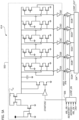
- Figure 1 is a circuit diagram exemplary of a memory reading architecture in a phase-change memory
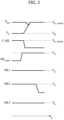
- Figure 2 is a time diagram exemplary of signals during a read operation in the memory of Figure 1 .
- a memory 10 may comprise an array of memory cells 102 (e.g., phase-change memory cells) arranged in bit lines 103B (here illustrated as vertical lines) and word lines 103W 1 , 103W 2 , 103W 3 (here illustrated as horizontal lines) according to a memory architecture known per se.
- each memory cell 102 may be arranged in series to a respective selection transistor 104 (e.g., a pnp BJT transistor) between a ground voltage terminal and the respective bit line 103B.
- the selection transistors 104 of a same word line 103W receive a same control signal at their control (e.g., base) terminals, e.g., control signals WL1 , WL2 , WL3 as exemplified in Figures 1 and 2 .
- Each bit line 103B may be selectively coupled (e.g., via a respective p-channel MOS transistor 106 having its current path in series to the bit line and receiving a control signal Y_SEL ) to a supply voltage rail 108 that provides a regulated voltage V REG .
- respective clamping transistors 110 may be coupled between each bit line 103B (e.g., at the source terminals of transistors 106) and the ground terminal.
- the clamping transistors 110 may receive the same control signal WL CLAMP at their control (e.g., base) terminals.
- Each bit line 103B has a respective capacitive load C BL due to the capacitances of the memory cells 102 and/or of the transistors 106, 110.
- a read operation in a phase-change memory as exemplified in Figure 1 may be carried out as exemplified in Figure 2 to read (and provide as output) the content of plural PCM words on an output data bus DATA OUT[144:0].
- information may be stored associating two cells to each bit: a SET cell (having low resistance and high current) and a RESET cell (having high resistance and low current).
- a memory sense circuit may read information from the cells in differential mode.
- two operations may be available to read the memory content, i.e.:
- T ACC the specification for the memory access time
- T ACC the specification for the memory access time
- read parallelism e.g., reading two words in parallel
- sensing of the content of the memory cells may be carried out in differential mode: a sensing circuit reads in differential mode from the bit line BL_SET and the bit line BL_RESET, so that the SET memory cell and the RESET memory cell are selected.
- the SET memory cell and the RESET memory cell are selected by properly driving the control signals (word selection signals) WL1 , WL2, WL3: for instance, as exemplified in Figure 2 , by keeping signals WL1 and WL3 at a high logic value (e.g., equal to a supply voltage V CC ) and by driving signal WL2 to a low logic value (e.g., equal to the ground voltage) cell 102s is selected as the SET cell and cell 102 R is selected as the RESET cell.
- word selection signals word selection signals
- WL1 , WL2, WL3 for instance, as exemplified in Figure 2 , by keeping signals WL1 and WL3 at a high logic value (e.g., equal to a supply voltage V CC ) and by driving signal WL2 to a low logic value (e.g., equal to the ground voltage) cell 102s is selected as the SET cell and cell 102 R is selected as the RESET cell.
- a voltage regulator (e.g., an LDO regulator) produces the regulated voltage V REG at the supply rail 108 (e.g., having an expected voltage value V BL_CHARGE ).
- the value V BL_CHARGE of voltage V REG should be high enough to provide a proper voltage stack to the bit lines to result in the correct values of the memory cells currents.
- the voltage V BL_ at the selected bit lines is clamped to the value V BE of the base-emitter voltage of the clamping transistors 110, and then the bit lines are pre-charged to the value V BL_CHARGE of the regulated voltage V REG by activating the transistors 106 (see in Figure 2 the control signal Y_SEL switching from a high value V BL_CHARGE to a low value to activate transistors 106).
- the control signals WL1 and WL3 of the unselected word lines are driven to a high voltage value (e.g., a supply voltage V CC ) so as to keep the respective selection transistors in a nonconductive state.
- bit lines are charged from the value V BE (e.g., about 0.5 V) to the value V BL_CHARGE (e.g., about 1.55 V).
- V BE e.g., about 0.5 V
- V BL_CHARGE e.g., about 1.55 V
- a relevant current flows from the supply rail 108 towards the bit lines, causing a relevant drop of the voltage V REG whose value decreases from the regulated value V BL_CHARGE (see again Figure 2 ).
- T REC short recovery time
- T ACC short access time
- the (LDO) voltage regulator should be able to provide a high current with a fast response time.
- V BL_CHARGE may be lower than V CC,MIN in typical cases but higher than V CC,MIN in some corner cases (e.g., slow silicon and high temperature) to compensate the selector and cell variations.
- V BL_CHARGE could be set higher to provide higher SET currents and reduce read fails. Therefore, the (LDO) voltage regulator may be demanded to provide the correct output voltage even if the supply voltage Vcc is lower than the expected regulated voltage V BL_CHARGE .
- Figure 3 is a circuit diagram exemplary of the circuit architecture of an LDO voltage regulator 30 for use in a memory device.
- the regulator comprises an input node 300 configured to receive an input voltage V CC (e.g., in the range of 1.6 V to 3.6 V) and an output node 302 configured to provide a regulated output voltage V REG (e.g., in the range of 1.6 V to 1.8 V).
- a pass element 304 e.g., a p-channel MOS transistor
- the terminal of the pass element 304 opposed to the output node 302 can be either directly connected to the input node 300 (when the input voltage V CC is higher than the output voltage V REG that the regulator 30 is expected to provide), or can be coupled to the output of a charge pump circuit 308 (when the input voltage Vcc is lower than the output voltage V REG ).
- the charge pump circuit 308 which is also coupled to the input node 300 to receive therefrom the input voltage V CC , may receive an enabling signal PMP_EN and a clock signal PMP_CK and may produce an output voltage higher than V CC as a function of signals PMP_EN and PMP_CK in a manner known per se.
- a large tank capacitance C TANK is coupled between the output node 302 and the ground node 310 and provides a charge reservoir to reduce undershoot of the output voltage V REG .
- the LDO regulator 30 also comprises a feedback network to produce the control signal for the pass element 304.
- the feedback network comprises a resistor R1 arranged in series to a variable current generator 312 between the output node 302 and the ground node 310.
- the amount of current generated by the current generator 312 may depend on a digital control signal VBL _ CTL ⁇ 4:0>.
- the node intermediate the resistor R1 and the current generator 312 may thus provide a feedback signal VFB that is provided at the inverting input of a high-voltage comparator 314.
- a reference voltage signal VREF is provided at the non-inverting input of the comparator 314.
- the comparator may receive a supply voltage from the node intermediate the pass element 304 and the selector 306, i.e., may receive either the supply voltage Vcc or the supply voltage produced by the charge pump 308, depending on the state of the selector 306.
- the output signal from the comparator 314 is provided as a control signal to the pass element 304.
- a big selector 306 (e.g., two big switches) is necessary to connect the input of the pass element 304 and the supply node of the comparator 314 to the input node 300 or to the output of the charge pump 308 (depending on the state of the selector 306, which depends on the difference between the values of V CC and V REG ). Also, a voltage detector is necessary to correctly operate the selector 306.
- One or more embodiments may rely on a different LDO voltage regulator architecture 40 as exemplified in Figure 4 , also referred to as on/off LDO regulator with integrated charge pump, which is also suitable for use in a memory device 10 as exemplified in Figure 1 .
- a voltage regulator 40 comprises an input node 400 configured to receive an input voltage V CC (e.g., in the range of 1.6 V to 3.6 V) and an output node 402 configured to provide a regulated output voltage V REG (e.g., in the range of 1.6 V to 1.8 V).
- V CC e.g., in the range of 1.6 V to 3.6 V
- V REG regulated output voltage
- One or more embodiments may comprise a first pass element 404a (e.g., an electronic switch, more specifically an n-channel MOS transistor) arranged between the input node 400 and the output node 402.
- the first pass element 404a When enabled, the first pass element 404a is selectively activatable (e.g., in an on-off manner) to provide a low-impedance current path between the input node 400 and the output node 402.
- the first pass element 404a may be enabled in response to the input voltage V CC being higher than the output voltage V REG that the regulator 40 is expected to provide, possibly by a margin ⁇ V.
- the channel of transistor 404a may have a width of about 200 ⁇ m and a length of about 0.3 ⁇ m.
- One or more embodiments may comprise a first feedback network configured to produce a control signal COMP OUT that controls the first pass element 404a.
- the first feedback network may comprise a resistance R1 (e.g., a resistor) arranged in series to a variable current generator 412 between the output node 402 and a ground node 410.
- the amount of current generated by the current generator 412, and thus the voltage drop across resistance R1 may depend on a digital control signal VBL CTL ⁇ 4:0> (e.g., a 5-bit signal).
- the node intermediate the resistance R1 and the current generator 412 may thus provide a feedback signal VFB that is fed to the inverting input of a low-voltage, high-speed comparator 414.
- a reference voltage signal VREF is fed to the non-inverting input of the comparator 414.
- the comparator 414 may receive from node 415 a supply voltage V DD that is lower than the supply voltage V CC at node 400 (for instance, V DD may be a power supply voltage in the range of 0.81 V to 1.15 V for low voltage transistors, and Vcc may be a power supply voltage in the range of 1.62 V to 3.6 V for high voltage transistors).
- the output signal COMP OUT from the comparator 414 is provided as a control signal to the first pass element 404a via a level shifter circuit 416a.
- the level shifter circuit 416a may receive a positive supply voltage VXR and a control signal VCC_EN produced by a second feedback network of the regulator circuit 40, and may be configured to shift the low voltage level from the output of comparator 414 to the VXR voltage domain.
- the level shifter 416a may be activated (e.g., turned on) in response to the control signal VCC_EN being asserted (e.g., set to '1').
- the level shifter 416a When turned on, the level shifter 416a shifts the signal COMP_OUT from the V DD voltage domain level (e.g., 0.81 V to 1.15 V) to the VXR voltage domain level (e.g., 3.6 V).
- the level shifter 416a may be deactivated (e.g., turned off) in response to the control signal VCC_EN being de-asserted (e.g., set to '0'), thereby forcing the gate of transistor 404a to a low value (e.g., 0 V) to turn it off.
- the control signal COMP OUT may thus be propagated to the control terminal of the first pass element 404a (e.g., to the gate terminal of transistor 404a), so that the first pass element 404a is activatable, depending on signal COMP OUT, when V CC is higher than the expected output voltage V BL_CHARGE plus a certain voltage margin ⁇ V ( V CC > V BL_CHARGE + ⁇ V).
- the gate of transistor 404a may be clocked to voltage VXR at a very high frequency, since comparator 414 operates at a high speed.
- One or more embodiments may comprise a charge pump circuit 408 coupled to the input node 400 to receive therefrom the input voltage Vcc.
- the charge pump circuit 408 may receive an enabling signal PMP_EN and the control signal COMP OUT and may produce an output voltage V BL_SUPPLY higher than V CC as a function of signals PMP_EN and COMP OUT as disclosed in the following.
- the charge pump 408 may be switched on (respectively, off) as a function of the enabling signal PMP_EN being asserted (respectively, de-asserted), while the ON/OFF switching activity of the clock phases of the output stages of the charge pump 408 may be controlled by signal COMP OUT. Therefore, in one or more embodiments the charge pump 408 may not be provided with a dedicated regulator, insofar as it may rely on (e.g., use) the (very fast) comparator 414 instead.
- One or more embodiments may comprise a second pass element 404b (e.g., an electronic switch, more specifically an n-channel MOS transistor) arranged between the output of the charge pump circuit 408 and the output node 402.
- the second pass element 404b is selectively activatable (e.g., in an on-off manner) to provide a low-impedance current path between the output of the charge pump circuit 408 and the output node 402.
- the second pass element 404b may be activated (e.g., switched to an ON state) in response to the input voltage Vcc being lower than the output voltage V REG that the regulator 40 is expected to provide.
- the channel of transistor 404b may have a width of about 200 ⁇ m and a length of about 0.36 ⁇ m.
- switching of the output node 402 between voltage Vcc (received from node 400 via pass element 404a) and voltage V BL_SUPPLY (received from circuit 408 via pass element 404b) may be managed dynamically.
- One or more embodiments may comprise a second feedback network configured to produce the control signals PMP_EN and VCC_EN.
- the second feedback network comprises a resistance R2 (e.g., a resistor) arranged in series to a variable current generator 418 between the input node 400 and the ground node 410.
- the amount of current generated by the current generator 418, and thus the voltage drop across resistance R2 may depend on a digital control signal VCC CTL ⁇ 2:0> (e.g., a 3-bit signal).
- the node intermediate the resistance R2 and the current generator 418 may thus provide a threshold signal VTH that is fed to the non-inverting input of a comparator 420.
- the output voltage V REG is fed to the inverting input of the comparator 420.
- the comparator 420 produces as output the control signal VCC_EN by comparing VTH to V REG .
- An inverter circuit 422 receives the control signal VCC_EN as input and produces the control signal PMP_EN as
- the control signal PMP_EN is provided as a control signal to the second pass element 404b via a level shifter circuit 416b.
- the level shifter circuit 416b may receive the positive supply voltage VXR and may be configured to shift the low voltage level from the output of comparator 420 to the VXR voltage domain.
- the control signal PMP_EN may thus be propagated to the control terminal of the second pass element 404b (e.g., to the gate terminal of transistor 404b), so that the second pass element 404b is activated when Vcc is lower than the expected output voltage V BL_CHARGE plus a certain voltage margin ⁇ V ( V CC ⁇ V BL_CHARGE + ⁇ V).
- the gate of transistor 404b may be forced to voltage VXR when signal PMP_EN is asserted, and the value V BL_CHARGE of the output voltage V REG may be regulated directly by the output V BL_SUPPLY of the charge pump circuit 408.
- the output voltage V REG may be driven to its regulated value V BL_CHARGE till when a control signal VBL_OK is asserted (e.g., set to ⁇ 1').
- the output voltage V REG may be kept at its regulated value V BL_CHARGE either by voltage Vcc or by voltage V BL_SUPPLY .
- the charge pump circuit 408 and the driver i.e., the level shifter 416b and the pass element 404b coupled between the pump 408 and the output node 402 may be switched on.
- the value of digital signal VCC CTL ⁇ 2:0> may be set to 2, so that the charge pump circuit is switched on when V CC - V REG ⁇ 80 mV.
- the charge pump circuit 408 may not be provided with an internal voltage regulator.
- the output stages may thus be directly controlled by the output of the comparator 414.
- one or more embodiments may not comprise a dedicated tank capacitor C TANK coupled between the output node 402 and the ground node 410.
- a large tank capacitance may be provided at the output node 402 by selectively connecting, during the read operations in the memory 10, all the unselected word lines (e.g., word lines 103W 1 and 103W 3 according to the example of Figures 1 and 2 ) of all the memory sectors to the output node 402 via respective switches 424 1 , ..., 424 3 .
- the switches 424 1 , ..., 424 3 may comprise n-channel MOS transistors.
- each n-channel MOS transistor 424 1 , ..., 424 3 may receive the respective control signal WL1 , WL2 or WL3 at the gate terminal.
- the total capacitance couplable to node 402 via the switches 424 may be approximately equal to 8*4* 1056* 180 fF ⁇ 6 nF.
- FIGS. 5A , 5B and 5C are circuit diagrams exemplary of possible implementation details of a voltage regulator circuit 40 according to one or more embodiments.
- Comparator 414 may comprise a high frequency ring oscillator 500 providing M different clock signals (or clock phases) CKA, CKB, CKC, CKD, CKE (e.g., five clock signals). Each clock signal may be delayed by a fraction 1/M (e.g., one fifth) of the ring oscillator period Tosc with respect to the preceding one. For instance, if the frequency of ring oscillator 500 is approximately 800 MHz, then Tosc is approximately 1.25 ns.
- Each of clock signals CKA, CKB, CKC, CKD, CKE may have a period of 1.25 ns, with signal CKB being delayed by 0.25 ns with respect to signal CKA, signal CKC being delayed by 0.25 ns with respect to signal CKB, and so on until signal CKA being delayed by 0.25 ns with respect to signal CKE.
- Each of the clock signals produced by the ring oscillator 500 may be used to clock a respective dynamic comparator 502A, ..., 502E.
- the comparators 502A, ..., 502E may thus operate sequentially in a quasi continuous mode, with each comparator 502A, ..., 502E being activated for a time period equal to Tosc/M (e.g., Tosc/5) and with the comparators 502A, ..., 502E being activated one after the other according to a "rotation" mechanism.
- the comparators 502A, ..., 502E may be provided with offset compensation circuitry.
- Each of comparators 502A, ..., 502E may receive the reference signal VREF at a respective non-inverting input and the feedback signal VFB at a respective inverting input.
- the dynamic comparators 502A, ..., 502E and the ring oscillator 500 may operate in a low supply voltage domain (e.g., 0.8 V to 1.15 V), so that low voltage transistors can be used and very high frequency can be reached.
- a low supply voltage domain e.g., 0.8 V to 1.15 V
- Use of an ultra high speed comparator 414 as exemplified in Figure 5A which relies on a high frequency ring oscillator 500 with very fast start/stop operation and temperature compensation, is thus advantageous insofar as the speed of the regulator 40 may depend mainly on the speed of comparator 414.
- the output signals from comparators 502A, ..., 502E are fed to a monostable circuit 504 that produces the control signal COMP OUT.
- the assertion and de-assertion of signal COMP OUT depends on the values of signals VREF and VFB at the input of the dynamic comparators 502.
- signal COMP_OUT will be asserted (e.g., set to ⁇ 1') and the pass element 404a will supply current to the output node 402.
- the monostable circuit 504 may be configured to generate a pulse in the output signal COMP OUT in response to a pulse being received from any of the dynamic comparators 502A, ..., 502E.
- circuit 504 operates as a monostable circuit insofar as it generates a stable output pulse that may be the composition of a plurality of input pulses (one or more).
- One or more embodiments may comprise a logic circuit 506 configured to control the switching activity of the ring oscillator 500 and of the comparators 502 based on read commands issued towards a memory.
- the ring oscillator 500 and the comparators 502 may be activated when a read command is issued (e.g., a read signal READSTART is asserted or set to ⁇ 1').
- the ring oscillator 500 and the comparators 502 may be refreshed (e.g., periodically) by a low frequency trimmable clock signal.
- the logic circuit 506 may produce an enabling signal COMP_EN for the comparators 502A, ..., 502E and a start signal STARTOSC for the oscillator 500 as a function of one or more of signals VBL_EN , READSTART, REFRESH, VBL_OK and CKA.
- signal COMP_EN may be asserted (e.g., set to '1') in response to signal VBL_EN being asserted (e.g., set to '1') indicating that the voltage regulator 40 is ON after power-on and signal VBL _ OK being asserted (e.g., set to '1') indicating that signal VREF is pre-charged to its steady state at power-on by another circuitry.
- signals VBL_EN and VBL _ OK are expected to remain asserted. Additionally, signal COMP_EN may be asserted when a pulse is generated in signal READSTART (indicating that a read command is issued). Signal COMP_EN may remain asserted for a certain time interval, e.g., depending on the state of a shift register clocked by one of the clock phases of the oscillator 500, e.g., clock signal CKA. Therefore, the voltage regulator 40 may be switched ON (only) for a reduced period necessary to perform a memory read operation. Signal REFRESH may be used to refresh the V REG signal (e.g., periodically insofar as it is a clocked structure).
- Figure 5B is exemplary of a possible implementation of the feedback networks that produce signals VFB, VCC_EN and PMP_EN.
- one or more embodiments may comprise a reference current generator circuit 508.
- the circuit 508 may comprise an operation amplifier 510 that produces a gate control signal for transistors 512, 514 and 516 (e.g., p-channel MOS transistors).
- Transistor 512 may have a certain width 10*W, a gate terminal coupled to the output of amplifier 510, a source terminal coupled to the supply node 400 to receive the supply voltage V CC , and a drain terminal coupled to a first terminal of a resistance R51 (e.g., a 123 kS2 resistor).
- the second terminal of resistance R51 may be coupled to the ground node 410.
- the non-inverting input of amplifier 510 may receive a bandgap reference voltage V BG and the inverting input of amplifier 510 may be coupled to a node intermediate transistor 512 and resistance R51.
- variable current generator 412 may comprise an adjustable current mirror arrangement including transistors 518, 520 and configured to mirror the current I REF output from transistor 516.
- the current mirror may comprise an n-channel MOS transistor 518 in transdiode configuration coupled to a variable n-channel MOS transistor 520 (e.g., a set of selectively activatable transistors 520 arranged in parallel) controlled by signal VBL CTL ⁇ 4:0>.
- Each bit of signal VBL CTL ⁇ 4:0> may control (e.g., switch ON/OFF) one of transistors 520 of the current mirror.
- variable transistor 520 may comprise (or consist of) five transistors, one for each bit of signal VBL CTL ⁇ 4:0>.
- the current flowing through resistance R1 and the voltage drop V 1 on resistance R1 can be controlled.
- Resistances R1 and R51 may be matched.
- One or more embodiments may comprise two transistors (e.g., n-channel MOS transistors) 522 and 524 coupled in series between the low-voltage supply node 415 to receive voltage V DD and the ground node.
- the gate of transistor 522 may be coupled to a node intermediate transistor 520 and resistance R1, and the feedback signal VFB may be produced at a node intermediate transistors 522 and 524.
- the transistors 522 and 524 may thus shift down the voltage at the gate of transistor 522. Also signal VREF may be shifted of the same amount.
- variable current generator 418 may comprise an adjustable current mirror arrangement including transistors 526, 528 and configured to mirror current I REF output from transistor 514.
- the current mirror may comprise an n-channel MOS transistor 526 in transdiode configuration coupled to a variable n-channel MOS transistor 528 (e.g., a set of selectively activatable transistors 528 arranged in parallel) controlled by signal VCC CTL ⁇ 2:0>.
- Each bit of signal VCC_CTL ⁇ 2:0 > may control (e.g., switch ON/OFF) one of transistors 528 of the current mirror.
- variable transistor 528 may comprise (or consist of) three transistors, one for each bit of signal VCC CTL ⁇ 2:0>.
- the current flowing through resistance R2 and the voltage drop V 2 on resistance R2 can be controlled.
- Resistances R2 and R51 may be matched.
- the first and second feedback networks of the regulator 40 may not be directly coupled to the output node 402 to receive voltage V REG (as shown in the simplified scheme of Figure 4 ).
- the feedback networks may be coupled to the unselected word lines of the memory array (e.g., via transistors 530 1 , ..., 530 3 ) to receive a voltage signal V REG_F , substantially corresponding to the supply voltage V REG as filtered by the capacitive load of the unselected word lines.
- V REG_F substantially corresponding to the supply voltage V REG as filtered by the capacitive load of the unselected word lines.
- such an arrangement may also prevent undesired switching.
- One or more embodiments of an LDO voltage regulator as exemplified herein may thus have a fast response time, e.g., resorting to high speed dynamic comparators 502A, ..., 502E in the comparator 414.
- one or more embodiments may provide high accuracy by resorting to offset compensation for the comparators 502A, ..., 502E.
- a large capacitance may be selectively coupled at the output node 402 of the voltage regulator by coupling thereto the unselected word lines (e.g., via switches 424) of a memory device to which the voltage regulator is coupled.
- Such arrangement facilitates providing a fast (e.g., almost instantaneous) current during the pre-charge phase without the need of resorting to a large, dedicated tank capacitance, thereby saving layout area (e.g., silicon area).
- one or more embodiments may comprise a charge pump circuit 408 integrated in the voltage regulator 40.
- the charge pump circuit 408 may be directly regulated by the output of dynamic comparator 414, resulting in a fast control and response time, as well as a reduction of the layout area insofar as the pump circuit 408 does not need a dedicated comparator, feedback circuit and related circuitry.
- one or more embodiments may provide a dynamic architecture for switching between the supply voltage Vcc and supply voltage V BL_SUPPLY produced by the pump 408, resulting in a reduction of the layout area insofar as a lower number of big switches (e.g., selectors) and related circuitry is needed.
- the dynamic switching architecture also results in a reduced current consumption and a higher efficiency of the charge pump circuit 408 insofar as there is no need to regulate the charge pump circuit 408 at a high voltage value.
- the dynamic switching architecture also allows to trim the difference ⁇ V between the supply voltage Vcc and the regulated voltage V REG , resulting in a higher degree of flexibility of the architecture and increased adaptability to different specifications (e.g., charge/discharge voltage supply ramp rate).
- hysteresis is introduced to avoid undesired switching.
- an on/off architecture facilitates limited and controlled standby current consumption and quiescent current consumption.
Landscapes
- Engineering & Computer Science (AREA)
- Power Engineering (AREA)
- Physics & Mathematics (AREA)
- Nonlinear Science (AREA)
- Electromagnetism (AREA)
- General Physics & Mathematics (AREA)
- Radar, Positioning & Navigation (AREA)
- Automation & Control Theory (AREA)
- Dc-Dc Converters (AREA)
- Continuous-Control Power Sources That Use Transistors (AREA)
Claims (13)
- Spannungsreglerschaltung (40), umfassend:einen Eingangsknoten (400), der so konfiguriert ist, dass er eine Eingangsversorgungsspannung (VCC ) empfängt;einen Ausgangsknoten (402), der so konfiguriert ist, dass er eine geregelte Ausgangsspannung (VREG ) erzeugt;ein erstes Rückkopplungsnetzwerk (R1, 412, 414), das so konfiguriert ist, dass es ein Rückkopplungssignal (VFB) erzeugt, das die geregelte Ausgangsspannung (VREG ) angibt, und das Rückkopplungssignal (VFB) mit einem Referenzsignal (VREF) vergleicht, um ein erstes gepulstes Steuersignal (COMP_OUT) zu erzeugen, wobei das erste gepulste Steuersignal (COMP_OUT) in Reaktion darauf, dass das Referenzsignal (VREF) höher ist als das Rückkopplungssignal (VFB), geltend gemacht wird und in Reaktion darauf, dass das Referenzsignal (VREF) niedriger ist als das Rückkopplungssignal (VFB), ungeltend gemacht wird, wodurch ein zeitgemittelter Wert des ersten gepulsten Steuersignals (COMP_OUT) von der Differenz zwischen dem Referenzsignal (VREF) und dem Rückkopplungssignal (VFB) abhängig ist;ein zweites Rückkopplungsnetzwerk (R2, 418, 420), das so konfiguriert ist, dass es ein Schwellensignal (VTH) erzeugt, das die Eingangsversorgungsspannung (VCC ) angibt, und die geregelte Ausgangsspannung (VREG ) mit dem Schwellensignal (VTH) vergleicht, um ein zweites Steuersignal (VCC_EN) zu erzeugen, wobei das zweite Steuersignal (VCC_EN) in Reaktion darauf, dass das Schwellensignal (VTH) höher ist als die geregelte Ausgangsspannung (VREG ), geltend gemacht wird und in Reaktion darauf, dass das Schwellensignal (VTH) niedriger ist als die geregelte Ausgangsspannung (VREG ) , ungeltend gemacht wird;eine Ladungspumpenschaltung (408), die so konfiguriert ist, dass sie eine Versorgungsspannung (VBL_SUPPLY ) erzeugt, die höher ist als die Eingangsversorgungsspannung (VCC ) , wobei die Ladungspumpenschaltung (408) in Reaktion darauf, dass das zweite Steuersignal (VCC_EN) ungeltend gemacht wird, aktiviert (PMP_EN) wird und durch das erste gepulste Steuersignal (COMP_OUT) getaktet wird, wodurch der Wert der Versorgungsspannung (VBL_SUPPLY ) vom ersten gepulsten Steuersignal (COMP_OUT) abhängig ist;ein erstes Durchgangselement (404a), das zwischen dem Eingangsknoten (400) und dem Ausgangsknoten (402) angeordnet ist, wobei das erste Durchgangselement (404a) in Reaktion darauf, dass das zweite Steuersignal (VCC_EN) geltend gemacht wird, aktiviert wird und in Reaktion darauf, dass das erste gepulste Steuersignal (COMP_OUT) geltend gemacht wird, selektiv aktiviert wird, um den Eingangsknoten (400) mit dem Ausgangsknoten (402) zu verbinden; undein zweites Durchgangselement (404b), das zwischen dem Ausgang der Ladungspumpenschaltung (408) und dem Ausgangsknoten (402) angeordnet ist, wobei das zweite Durchgangselement (404b) in Reaktion darauf, dass das zweite Steuersignal (VCC_EN) ungeltend gemacht wird, selektiv aktiviert wird, um den Ausgang der Ladungspumpenschaltung (408) mit dem Ausgangsknoten (402) zu verbinden.
- Spannungsreglerschaltung (40) nach Anspruch 1, wobei das erste Rückkopplungsnetzwerk (R1, 412, 414) einen getakteten Niederspannungskomparator (414) umfasst, der so konfiguriert ist, dass er das Rückkopplungssignal (VFB) mit dem Referenzsignal (VREF) vergleicht, um in Reaktion darauf, dass das Referenzsignal (VREF) höher ist als das Rückkopplungssignal (VFB), das erste gepulste Steuersignal (COMP_OUT) geltend zu machen, und in Reaktion darauf, dass das Referenzsignal (VREF) niedriger ist als das Rückkopplungssignal (VFB), das erste gepulste Steuersignal (COMP_OUT) ungeltend zu machen.
- Spannungsreglerschaltung (40) nach Anspruch 2, wobei der getaktete Niederspannungskomparator (414) umfasst:eine Vielzahl von dynamischen Komparatoren (502A, ..., 502E), die durch jeweilige zeitverschobene Taktsignale (CKA, ..., CKE) getaktet werden, wobei die jeweiligen Taktsignale (CKA, ..., CKE) die gleiche Taktperiode aufweisen und zueinander um einen Bruchteil der Taktperiode zeitverschoben sind, wobei die dynamischen Komparatoren (502A, ..., 502E) in der Vielzahl von dynamischen Komparatoren (502A, ..., 502E) so konfiguriert sind, dass sie das Rückkopplungssignal (VFB) sequentiell mit dem Referenzsignal (VREF) vergleichen, um in Reaktion darauf, dass das Referenzsignal (VREF) höher bzw. niedriger ist als das Rückkopplungssignal (VFB), jeweilige Ausgangssignale geltend bzw. ungeltend zu machen; undeine monostabile Schaltung (504), die so konfiguriert ist, dass sie die Ausgangssignale von der Vielzahl von dynamischen Komparatoren (502A, ..., 502E) empfängt und in Reaktion auf Geltendmachung eines der Ausgangssignale, die von der Vielzahl von dynamischen Komparatoren (502A, ..., 502E) empfangen werden, das erste gepulste Steuersignal (COMP_OUT) geltend macht.
- Spannungsreglerschaltung (40) nach Anspruch 3, wobei der getaktete Niederspannungskomparator (414) einen Ringoszillator (500) umfasst, der so konfiguriert ist, dass er die zeitverschobenen Taktsignale (CKA, ..., CKE) für die Vielzahl von dynamischen Komparatoren (502A, ..., 502E) erzeugt.
- Spannungsreglerschaltung (40) nach einem der Ansprüche 2 bis 4, die eine erste Pegelschieberschaltung (416a) umfasst, die zwischen dem getakteten Niederspannungskomparator (414) und dem ersten Durchgangselement (404a) angeordnet ist, wobei die erste Pegelschieberschaltung (416a) so konfiguriert ist, dass sie in Reaktion darauf, dass das zweite Steuersignal (VCC_EN) geltend gemacht wird, das erste gepulste Steuersignal (COMP_OUT) von einem Niederspannungsbereich (VDD ) in einen Hochspannungsbereich (VXR) verschiebt und das verschobene erste gepulste Steuersignal an das erste Durchgangselement (404a) weiterleitet.
- Spannungsreglerschaltung (40) nach einem der vorstehenden Ansprüche, wobei das erste Rückkopplungsnetzwerk (R1, 412, 414) einen ersten Widerstand (R1) umfasst, der mit einem ersten Stromgenerator (412) zwischen dem Ausgangsknoten (402) und einem Masseknoten (410) in Reihe angeordnet ist, wobei das Rückkopplungssignal (VFB) an einem Knoten zwischen dem ersten Widerstand (R1) und dem ersten Stromgenerator (412) erzeugt wird.
- Spannungsreglerschaltung (40) nach Anspruch 6, wobei der erste Stromgenerator (412) einen variablen Stromgenerator umfasst, der so konfiguriert ist, dass er einen variablen Strom in Abhängigkeit vom Wert eines ersten digitalen Steuersignals (VBL_CTL<4:0>) erzeugt, wodurch das Rückkopplungssignal (VFB) in Abhängigkeit vom ersten digitalen Steuersignal (VBL_CTL<4:0>) verschoben wird.
- Spannungsreglerschaltung (40) nach einem der vorstehenden Ansprüche, wobei das zweite Rückkopplungsnetzwerk (R2, 418, 420) umfasst:einen zweiten Widerstand (R2), der mit einem zweiten Stromgenerator (418) zwischen dem Eingangsknoten (400) und einem Masseknoten (410) in Reihe angeordnet ist, wobei das Schwellensignal (VTH) an einem Knoten zwischen dem zweiten Widerstand (R2) und dem zweiten Stromgenerator (418) erzeugt wird, undeinen weiteren Komparator (420), der so konfiguriert ist, dass er die geregelte Ausgangsspannung (VREG ) mit dem Schwellensignal (VTH) vergleicht, um in Reaktion darauf, dass das Schwellensignal (VTH) höher ist als die geregelte Ausgangsspannung (VREG ) , das zweite Steuersignal (VCC_EN) geltend zu machen und in Reaktion darauf, dass das Schwellensignal (VTH) niedriger ist als die geregelte Ausgangsspannung (VREG ) , das zweite Steuersignal (VCC_EN) ungeltend zu machen.
- Spannungsreglerschaltung (40) nach Anspruch 8, wobei der zweite Stromgenerator (418) einen variablen Stromgenerator umfasst, der so konfiguriert ist, dass er einen variablen Strom in Abhängigkeit vom Wert eines zweiten digitalen Steuersignals (VCC_CTL<2:0>) erzeugt, wodurch das Schwellensignal (VFB) in Abhängigkeit vom zweiten digitalen Steuersignal (VCC_CTL<2:0>) verschoben wird.
- Spannungsreglerschaltung (40) nach Anspruch 8 oder Anspruch 9, die eine Inverterschaltung (422) und eine zweite Pegelschieberschaltung (416b) umfasst, die zwischen dem weiteren Komparator (420) und dem zweiten Durchgangselement (404b) angeordnet sind, um ein komplementäres Signal (PMP_EN) des zweiten Steuersignals (VCC_EN) zu erzeugen, das komplementäre Signal (PMP_EN) von einem Niederspannungsbereich (VDD ) in einen Hochspannungsbereich (VXR) zu verschieben, und das verschobene komplementäre Signal (PMP_EN) an das zweite Durchgangselement (404b) weiterzuleiten, wobei das zweite Durchgangselement (404b) in Reaktion darauf, dass das verschobene komplementäre Signal (PMP_EN) geltend gemacht wird, aktiviert wird und in Reaktion darauf, dass das verschobene komplementäre Signal (PMP_EN) ungeltend gemacht wird, deaktiviert wird.
- Speichervorrichtung (10), umfassend:ein Array von Speicherzellen (102), die in einer Vielzahl von Bitleitungen (103B) und einer Vielzahl von Wortleitungen (103W1, 103W2, 103W3) angeordnet sind, wobei jede Speicherzelle (102) mit einem jeweiligen Auswahltransistor (104) zwischen einem Masseanschluss und der entsprechenden Bitleitung (103B) in Reihe angeordnet ist, und jede Bitleitung (103B) selektiv mit einer Versorgungsspannungsschiene (108), die eine geregelte Spannung (VREG) bereitstellt, gekoppelt (106, Y_SEL) werden kann; undeine Spannungsreglerschaltung (40) nach einem der vorstehenden Ansprüche, die den Ausgangsknoten (402) aufweist, der mit der Versorgungsspannungsschiene (108) gekoppelt ist, um ihr die geregelte Spannung (VREG) bereitzustellen;wobei die Spannungsreglerschaltung (40) in Reaktion darauf, dass ein Speicherlesebefehl von der Speichervorrichtung (10) empfangen wird, selektiv aktiviert wird, um die geregelte Spannung (VREG) zu erzeugen.
- Speichervorrichtung (10) nach Anspruch 11, wobei die Wortleitungen (103W1, ..., 103W3) selektiv mit dem Ausgangsknoten (402) der Spannungsreglerschaltung (40) gekoppelt (4241, ..., 4243) werden können, wobei die Speichervorrichtung so konfiguriert ist, dass sie während eines Lesevorgangs aus einer ausgewählten Wortleitung (103W2) in der Speichervorrichtung (10) eine oder mehrere nicht ausgewählte Wortleitungen (103W1, 103W3) mit dem Ausgangsknoten (402) der Spannungsreglerschaltung (40) koppelt.
- Speichervorrichtung (10) nach Anspruch 12, wobei:eine gefilterte Ausgangsspannung (VREG_F ) an der einen oder den mehreren nicht ausgewählten Wortleitungen (103W1, 103W3) , die mit dem Ausgangsknoten (402) der Spannungsreglerschaltung (40) gekoppelt sind, erzeugt wird;das erste Rückkopplungsnetzwerk (R1, 412, 414) der Spannungsreglerschaltung (40) selektiv mit den nicht ausgewählten Wortleitungen (103W1, 103W3) gekoppelt (5301, 5303) werden kann und so konfiguriert ist, dass es das Rückkopplungssignal (VFB) erzeugt, das die gefilterte Ausgangsspannung (VREG_F ) angibt; unddas zweite Rückkopplungsnetzwerk (R2, 418, 420) der Spannungsreglerschaltung (40) selektiv mit den nicht ausgewählten Wortleitungen (103W1, 103W3) gekoppelt (5301, 5303) werden kann und so konfiguriert ist, dass es die gefilterte Ausgangsspannung (VREG_F ) mit dem Schwellensignal (VTH) vergleicht, um das zweite Steuersignal (VCC_EN) zu erzeugen.
Applications Claiming Priority (1)
| Application Number | Priority Date | Filing Date | Title |
|---|---|---|---|
| IT202100027458 | 2021-10-26 |
Publications (2)
| Publication Number | Publication Date |
|---|---|
| EP4174859A1 EP4174859A1 (de) | 2023-05-03 |
| EP4174859B1 true EP4174859B1 (de) | 2024-08-21 |
Family
ID=79019134
Family Applications (1)
| Application Number | Title | Priority Date | Filing Date |
|---|---|---|---|
| EP22192488.9A Active EP4174859B1 (de) | 2021-10-26 | 2022-08-26 | Spannungsreglerschaltung und entsprechende speichervorrichtung |
Country Status (3)
| Country | Link |
|---|---|
| US (1) | US11803202B2 (de) |
| EP (1) | EP4174859B1 (de) |
| CN (1) | CN116027843B (de) |
Families Citing this family (7)
| Publication number | Priority date | Publication date | Assignee | Title |
|---|---|---|---|---|
| US11966241B2 (en) | 2021-07-09 | 2024-04-23 | Taiwan Semiconductor Manufacturing Company, Ltd. | Low dropout regulator circuits, input/output device, and methods for operating a low dropout regulator |
| US12386374B2 (en) * | 2023-05-30 | 2025-08-12 | Taiwan Semiconductor Manufacturing Company, Ltd. | Push-pull low-dropout (LDO) voltage regulator |
| CN116974324B (zh) * | 2023-08-28 | 2025-10-24 | 芯海科技(深圳)股份有限公司 | 带隙基准电路、基准电压产生方法、芯片及电子设备 |
| US20250124856A1 (en) * | 2023-10-12 | 2025-04-17 | Google Llc | System and method for reducing power consumed by a display |
| WO2025117229A1 (en) * | 2023-11-29 | 2025-06-05 | Rambus Inc. | Calibration of process, temperature, and supply compensated regulator |
| EP4593016A1 (de) * | 2024-01-29 | 2025-07-30 | STMicroelectronics International N.V. | Verfahren zur initialisierung von bitleitungen in phasenwechselspeichern, entsprechende vorrichtung und computerprogrammprodukt |
| CN120447675B (zh) * | 2025-07-10 | 2025-09-16 | 安徽大学 | 具有高压补偿的瞬态响应增强型ldo复合电路、模块 |
Family Cites Families (18)
| Publication number | Priority date | Publication date | Assignee | Title |
|---|---|---|---|---|
| US6262567B1 (en) * | 1997-08-01 | 2001-07-17 | Lsi Logic Corporation | Automatic power supply sensing with on-chip regulation |
| US6597158B2 (en) * | 2001-01-29 | 2003-07-22 | Seiko Epson Corporation | Adjustable current consumption power supply apparatus |
| JP2002258955A (ja) * | 2001-02-27 | 2002-09-13 | Toshiba Corp | 半導体装置 |
| FR2838840B1 (fr) * | 2002-04-23 | 2005-04-01 | St Microelectronics Sa | Comparateur de tension d'alimentation |
| US6828836B1 (en) * | 2003-09-09 | 2004-12-07 | National Semiconductor Corporation | Two comparator voltage mode PWM |
| ITMI20031924A1 (it) * | 2003-10-07 | 2005-04-08 | Atmel Corp | Convertitore da digitale ad analogico ad alta precisione con consumo di energia ottimizzato. |
| US20060082351A1 (en) * | 2004-10-15 | 2006-04-20 | Martins Marcus M | Low power operation of back-up power supply |
| ITMI20060758A1 (it) * | 2006-04-14 | 2007-10-15 | Atmel Corp | Metodo e circuito per l'alimentazione di tensione per circuiteria di orologio a tempo reale basata su una pompa di carica a tensione regolata |
| CN101286693B (zh) * | 2007-04-10 | 2011-03-30 | 立锜科技股份有限公司 | 电荷泵调节器及产生一受调节的电压的方法 |
| CN101667774B (zh) * | 2008-09-02 | 2012-05-16 | 北京兆易创新科技有限公司 | 一种闭环控制电荷泵电路 |
| IT1397283B1 (it) * | 2009-11-30 | 2013-01-04 | St Microelectronics Rousset | Stadio a pompa di carica, metodo di controllo di uno stadio a pompa di carica e memoria comprendente uno stadio a pompa di carica. |
| EP2997433B1 (de) * | 2013-05-17 | 2020-07-15 | Intel Corporation | On-chip versorgungsgenerator mit dynamischer schaltungsreferenz |
| US9703303B2 (en) * | 2014-04-25 | 2017-07-11 | Nxp Usa, Inc. | Charge pump LDO with secondary sensing for low power need based refresh |
| US9923457B2 (en) * | 2015-04-23 | 2018-03-20 | Taiwan Semiconductor Manufacturing Company, Ltd. | Regulated power converter and method of operating the same |
| IT201700035474A1 (it) * | 2017-03-31 | 2018-10-01 | St Microelectronics Srl | Circuito regolatore di tensione, dispositivo, apparecchiatura e procedimento corrispondenti |
| US10447160B2 (en) * | 2017-05-16 | 2019-10-15 | Semiconductor Components Industries, Llc | Pulse width control for switching mode power converters |
| US10177746B1 (en) * | 2018-07-20 | 2019-01-08 | Winbond Electronics Corp. | Overdrive Voltage Generator |
| JP2022144011A (ja) * | 2021-03-18 | 2022-10-03 | キオクシア株式会社 | 電源回路及び半導体集積回路 |
-
2022
- 2022-08-26 EP EP22192488.9A patent/EP4174859B1/de active Active
- 2022-09-21 US US17/933,972 patent/US11803202B2/en active Active
- 2022-10-25 CN CN202211313207.5A patent/CN116027843B/zh active Active
Also Published As
| Publication number | Publication date |
|---|---|
| CN116027843A (zh) | 2023-04-28 |
| US20230130268A1 (en) | 2023-04-27 |
| EP4174859A1 (de) | 2023-05-03 |
| CN116027843B (zh) | 2025-02-25 |
| US11803202B2 (en) | 2023-10-31 |
Similar Documents
| Publication | Publication Date | Title |
|---|---|---|
| EP4174859B1 (de) | Spannungsreglerschaltung und entsprechende speichervorrichtung | |
| US12555620B2 (en) | Memory device | |
| KR0156607B1 (ko) | 계층적 전원구조를 갖는 반도체집적회로장치 | |
| US7859322B2 (en) | Internal power-supply circuit | |
| US7948809B2 (en) | Regulator and semiconductor device | |
| US20220179439A1 (en) | Reference voltage generation | |
| US7750727B2 (en) | Voltage generating circuit | |
| US5940322A (en) | Constant voltage generating circuit with improved line voltage control | |
| US8217684B2 (en) | Fast and accurate current driver with zero standby current and features for boost and temperature compensation for MRAM write circuit | |
| US8194476B2 (en) | Semiconductor memory device and method for operating the same | |
| US20220157390A1 (en) | Memory system capable of reducing the reading time | |
| US8339871B2 (en) | Voltage sensing circuit capable of controlling a pump voltage stably generated in a low voltage environment | |
| US7286417B2 (en) | Low power dissipation voltage generator | |
| US7602168B2 (en) | Voltage regulator for integrated circuits | |
| US6330173B1 (en) | Semiconductor integrated circuit comprising step-up voltage generation circuit | |
| US20120218019A1 (en) | Internal voltage generating circuit and testing method of integrated circuit using the same | |
| US8879338B2 (en) | Semiconductor integrated circuit and nonvolatile semiconductor storage device | |
| JP3869690B2 (ja) | 内部電圧レベル制御回路および半導体記憶装置並びにそれらの制御方法 | |
| JP4259739B2 (ja) | 半導体記憶装置 | |
| US20130070542A1 (en) | Replica Circuit and It's Applications | |
| US12362001B2 (en) | Voltage generating circuit and memory | |
| KR100861302B1 (ko) | 칼럼 선택 드라이버의 동작전압 공급 장치 및 그 방법 | |
| CN117672294A (zh) | 电压生成电路及存储器 | |
| KR100780635B1 (ko) | 반도체 메모리 소자 및 그의 코어전압 발생방법 | |
| KR20030035311A (ko) | 고속 반도체 장치에 채용하기 적합한 내부전원 전압발생회로 및 그에 따른 내부전원전압 발생방법 |
Legal Events
| Date | Code | Title | Description |
|---|---|---|---|
| PUAI | Public reference made under article 153(3) epc to a published international application that has entered the european phase |
Free format text: ORIGINAL CODE: 0009012 |
|
| STAA | Information on the status of an ep patent application or granted ep patent |
Free format text: STATUS: THE APPLICATION HAS BEEN PUBLISHED |
|
| AK | Designated contracting states |
Kind code of ref document: A1 Designated state(s): AL AT BE BG CH CY CZ DE DK EE ES FI FR GB GR HR HU IE IS IT LI LT LU LV MC MK MT NL NO PL PT RO RS SE SI SK SM TR |
|
| STAA | Information on the status of an ep patent application or granted ep patent |
Free format text: STATUS: REQUEST FOR EXAMINATION WAS MADE |
|
| 17P | Request for examination filed |
Effective date: 20230712 |
|
| RBV | Designated contracting states (corrected) |
Designated state(s): AL AT BE BG CH CY CZ DE DK EE ES FI FR GB GR HR HU IE IS IT LI LT LU LV MC MK MT NL NO PL PT RO RS SE SI SK SM TR |
|
| GRAP | Despatch of communication of intention to grant a patent |
Free format text: ORIGINAL CODE: EPIDOSNIGR1 |
|
| RIC1 | Information provided on ipc code assigned before grant |
Ipc: G05F 1/575 20060101ALI20240325BHEP Ipc: G11C 11/4074 20060101ALI20240325BHEP Ipc: G11C 11/22 20060101ALI20240325BHEP Ipc: G11C 16/30 20060101ALI20240325BHEP Ipc: G11C 11/16 20060101ALI20240325BHEP Ipc: G11C 13/00 20060101ALI20240325BHEP Ipc: G05F 1/10 20060101ALI20240325BHEP Ipc: G11C 5/14 20060101AFI20240325BHEP |
|
| STAA | Information on the status of an ep patent application or granted ep patent |
Free format text: STATUS: GRANT OF PATENT IS INTENDED |
|
| INTG | Intention to grant announced |
Effective date: 20240502 |
|
| RIN1 | Information on inventor provided before grant (corrected) |
Inventor name: TOMAIUOLO, FRANCESCO Inventor name: MACCARRONE, AGATINO MASSIMO Inventor name: PISASALE, MICHELANGELO Inventor name: CONTE, ANTONINO Inventor name: RUTA, MARCO |
|
| GRAS | Grant fee paid |
Free format text: ORIGINAL CODE: EPIDOSNIGR3 |
|
| GRAA | (expected) grant |
Free format text: ORIGINAL CODE: 0009210 |
|
| STAA | Information on the status of an ep patent application or granted ep patent |
Free format text: STATUS: THE PATENT HAS BEEN GRANTED |
|
| AK | Designated contracting states |
Kind code of ref document: B1 Designated state(s): AL AT BE BG CH CY CZ DE DK EE ES FI FR GB GR HR HU IE IS IT LI LT LU LV MC MK MT NL NO PL PT RO RS SE SI SK SM TR |
|
| REG | Reference to a national code |
Ref country code: GB Ref legal event code: FG4D |
|
| REG | Reference to a national code |
Ref country code: CH Ref legal event code: EP |
|
| REG | Reference to a national code |
Ref country code: IE Ref legal event code: FG4D |
|
| REG | Reference to a national code |
Ref country code: DE Ref legal event code: R096 Ref document number: 602022005449 Country of ref document: DE |
|
| REG | Reference to a national code |
Ref country code: LT Ref legal event code: MG9D |
|
| REG | Reference to a national code |
Ref country code: NL Ref legal event code: MP Effective date: 20240821 |
|
| PG25 | Lapsed in a contracting state [announced via postgrant information from national office to epo] |
Ref country code: NO Free format text: LAPSE BECAUSE OF FAILURE TO SUBMIT A TRANSLATION OF THE DESCRIPTION OR TO PAY THE FEE WITHIN THE PRESCRIBED TIME-LIMIT Effective date: 20241121 |
|
| REG | Reference to a national code |
Ref country code: AT Ref legal event code: MK05 Ref document number: 1716329 Country of ref document: AT Kind code of ref document: T Effective date: 20240821 |
|
| PG25 | Lapsed in a contracting state [announced via postgrant information from national office to epo] |
Ref country code: FI Free format text: LAPSE BECAUSE OF FAILURE TO SUBMIT A TRANSLATION OF THE DESCRIPTION OR TO PAY THE FEE WITHIN THE PRESCRIBED TIME-LIMIT Effective date: 20240821 Ref country code: NL Free format text: LAPSE BECAUSE OF FAILURE TO SUBMIT A TRANSLATION OF THE DESCRIPTION OR TO PAY THE FEE WITHIN THE PRESCRIBED TIME-LIMIT Effective date: 20240821 Ref country code: PL Free format text: LAPSE BECAUSE OF FAILURE TO SUBMIT A TRANSLATION OF THE DESCRIPTION OR TO PAY THE FEE WITHIN THE PRESCRIBED TIME-LIMIT Effective date: 20240821 Ref country code: GR Free format text: LAPSE BECAUSE OF FAILURE TO SUBMIT A TRANSLATION OF THE DESCRIPTION OR TO PAY THE FEE WITHIN THE PRESCRIBED TIME-LIMIT Effective date: 20241122 Ref country code: PT Free format text: LAPSE BECAUSE OF FAILURE TO SUBMIT A TRANSLATION OF THE DESCRIPTION OR TO PAY THE FEE WITHIN THE PRESCRIBED TIME-LIMIT Effective date: 20241223 |
|
| PG25 | Lapsed in a contracting state [announced via postgrant information from national office to epo] |
Ref country code: BG Free format text: LAPSE BECAUSE OF FAILURE TO SUBMIT A TRANSLATION OF THE DESCRIPTION OR TO PAY THE FEE WITHIN THE PRESCRIBED TIME-LIMIT Effective date: 20240821 |
|
| PG25 | Lapsed in a contracting state [announced via postgrant information from national office to epo] |
Ref country code: LV Free format text: LAPSE BECAUSE OF FAILURE TO SUBMIT A TRANSLATION OF THE DESCRIPTION OR TO PAY THE FEE WITHIN THE PRESCRIBED TIME-LIMIT Effective date: 20240821 |
|
| PG25 | Lapsed in a contracting state [announced via postgrant information from national office to epo] |
Ref country code: AT Free format text: LAPSE BECAUSE OF FAILURE TO SUBMIT A TRANSLATION OF THE DESCRIPTION OR TO PAY THE FEE WITHIN THE PRESCRIBED TIME-LIMIT Effective date: 20240821 Ref country code: IS Free format text: LAPSE BECAUSE OF FAILURE TO SUBMIT A TRANSLATION OF THE DESCRIPTION OR TO PAY THE FEE WITHIN THE PRESCRIBED TIME-LIMIT Effective date: 20241221 |
|
| PG25 | Lapsed in a contracting state [announced via postgrant information from national office to epo] |
Ref country code: HR Free format text: LAPSE BECAUSE OF FAILURE TO SUBMIT A TRANSLATION OF THE DESCRIPTION OR TO PAY THE FEE WITHIN THE PRESCRIBED TIME-LIMIT Effective date: 20240821 |
|
| PG25 | Lapsed in a contracting state [announced via postgrant information from national office to epo] |
Ref country code: RS Free format text: LAPSE BECAUSE OF FAILURE TO SUBMIT A TRANSLATION OF THE DESCRIPTION OR TO PAY THE FEE WITHIN THE PRESCRIBED TIME-LIMIT Effective date: 20241121 Ref country code: ES Free format text: LAPSE BECAUSE OF FAILURE TO SUBMIT A TRANSLATION OF THE DESCRIPTION OR TO PAY THE FEE WITHIN THE PRESCRIBED TIME-LIMIT Effective date: 20240821 |
|
| PG25 | Lapsed in a contracting state [announced via postgrant information from national office to epo] |
Ref country code: RS Free format text: LAPSE BECAUSE OF FAILURE TO SUBMIT A TRANSLATION OF THE DESCRIPTION OR TO PAY THE FEE WITHIN THE PRESCRIBED TIME-LIMIT Effective date: 20241121 Ref country code: PT Free format text: LAPSE BECAUSE OF FAILURE TO SUBMIT A TRANSLATION OF THE DESCRIPTION OR TO PAY THE FEE WITHIN THE PRESCRIBED TIME-LIMIT Effective date: 20241223 Ref country code: PL Free format text: LAPSE BECAUSE OF FAILURE TO SUBMIT A TRANSLATION OF THE DESCRIPTION OR TO PAY THE FEE WITHIN THE PRESCRIBED TIME-LIMIT Effective date: 20240821 Ref country code: NO Free format text: LAPSE BECAUSE OF FAILURE TO SUBMIT A TRANSLATION OF THE DESCRIPTION OR TO PAY THE FEE WITHIN THE PRESCRIBED TIME-LIMIT Effective date: 20241121 Ref country code: NL Free format text: LAPSE BECAUSE OF FAILURE TO SUBMIT A TRANSLATION OF THE DESCRIPTION OR TO PAY THE FEE WITHIN THE PRESCRIBED TIME-LIMIT Effective date: 20240821 Ref country code: LV Free format text: LAPSE BECAUSE OF FAILURE TO SUBMIT A TRANSLATION OF THE DESCRIPTION OR TO PAY THE FEE WITHIN THE PRESCRIBED TIME-LIMIT Effective date: 20240821 Ref country code: IS Free format text: LAPSE BECAUSE OF FAILURE TO SUBMIT A TRANSLATION OF THE DESCRIPTION OR TO PAY THE FEE WITHIN THE PRESCRIBED TIME-LIMIT Effective date: 20241221 Ref country code: HR Free format text: LAPSE BECAUSE OF FAILURE TO SUBMIT A TRANSLATION OF THE DESCRIPTION OR TO PAY THE FEE WITHIN THE PRESCRIBED TIME-LIMIT Effective date: 20240821 Ref country code: GR Free format text: LAPSE BECAUSE OF FAILURE TO SUBMIT A TRANSLATION OF THE DESCRIPTION OR TO PAY THE FEE WITHIN THE PRESCRIBED TIME-LIMIT Effective date: 20241122 Ref country code: FI Free format text: LAPSE BECAUSE OF FAILURE TO SUBMIT A TRANSLATION OF THE DESCRIPTION OR TO PAY THE FEE WITHIN THE PRESCRIBED TIME-LIMIT Effective date: 20240821 Ref country code: ES Free format text: LAPSE BECAUSE OF FAILURE TO SUBMIT A TRANSLATION OF THE DESCRIPTION OR TO PAY THE FEE WITHIN THE PRESCRIBED TIME-LIMIT Effective date: 20240821 Ref country code: BG Free format text: LAPSE BECAUSE OF FAILURE TO SUBMIT A TRANSLATION OF THE DESCRIPTION OR TO PAY THE FEE WITHIN THE PRESCRIBED TIME-LIMIT Effective date: 20240821 Ref country code: AT Free format text: LAPSE BECAUSE OF FAILURE TO SUBMIT A TRANSLATION OF THE DESCRIPTION OR TO PAY THE FEE WITHIN THE PRESCRIBED TIME-LIMIT Effective date: 20240821 |
|
| PG25 | Lapsed in a contracting state [announced via postgrant information from national office to epo] |
Ref country code: DK Free format text: LAPSE BECAUSE OF FAILURE TO SUBMIT A TRANSLATION OF THE DESCRIPTION OR TO PAY THE FEE WITHIN THE PRESCRIBED TIME-LIMIT Effective date: 20240821 Ref country code: SM Free format text: LAPSE BECAUSE OF FAILURE TO SUBMIT A TRANSLATION OF THE DESCRIPTION OR TO PAY THE FEE WITHIN THE PRESCRIBED TIME-LIMIT Effective date: 20240821 Ref country code: RO Free format text: LAPSE BECAUSE OF FAILURE TO SUBMIT A TRANSLATION OF THE DESCRIPTION OR TO PAY THE FEE WITHIN THE PRESCRIBED TIME-LIMIT Effective date: 20240821 |
|
| PG25 | Lapsed in a contracting state [announced via postgrant information from national office to epo] |
Ref country code: LU Free format text: LAPSE BECAUSE OF NON-PAYMENT OF DUE FEES Effective date: 20240826 |
|
| PG25 | Lapsed in a contracting state [announced via postgrant information from national office to epo] |
Ref country code: EE Free format text: LAPSE BECAUSE OF FAILURE TO SUBMIT A TRANSLATION OF THE DESCRIPTION OR TO PAY THE FEE WITHIN THE PRESCRIBED TIME-LIMIT Effective date: 20240821 |
|
| PG25 | Lapsed in a contracting state [announced via postgrant information from national office to epo] |
Ref country code: CZ Free format text: LAPSE BECAUSE OF FAILURE TO SUBMIT A TRANSLATION OF THE DESCRIPTION OR TO PAY THE FEE WITHIN THE PRESCRIBED TIME-LIMIT Effective date: 20240821 |
|
| PG25 | Lapsed in a contracting state [announced via postgrant information from national office to epo] |
Ref country code: IT Free format text: LAPSE BECAUSE OF FAILURE TO SUBMIT A TRANSLATION OF THE DESCRIPTION OR TO PAY THE FEE WITHIN THE PRESCRIBED TIME-LIMIT Effective date: 20240821 Ref country code: SK Free format text: LAPSE BECAUSE OF FAILURE TO SUBMIT A TRANSLATION OF THE DESCRIPTION OR TO PAY THE FEE WITHIN THE PRESCRIBED TIME-LIMIT Effective date: 20240821 |
|
| REG | Reference to a national code |
Ref country code: DE Ref legal event code: R097 Ref document number: 602022005449 Country of ref document: DE |
|
| REG | Reference to a national code |
Ref country code: BE Ref legal event code: MM Effective date: 20240831 |
|
| PLBE | No opposition filed within time limit |
Free format text: ORIGINAL CODE: 0009261 |
|
| STAA | Information on the status of an ep patent application or granted ep patent |
Free format text: STATUS: NO OPPOSITION FILED WITHIN TIME LIMIT |
|
| PG25 | Lapsed in a contracting state [announced via postgrant information from national office to epo] |
Ref country code: MC Free format text: LAPSE BECAUSE OF FAILURE TO SUBMIT A TRANSLATION OF THE DESCRIPTION OR TO PAY THE FEE WITHIN THE PRESCRIBED TIME-LIMIT Effective date: 20240821 |
|
| PG25 | Lapsed in a contracting state [announced via postgrant information from national office to epo] |
Ref country code: BE Free format text: LAPSE BECAUSE OF NON-PAYMENT OF DUE FEES Effective date: 20240831 |
|
| PG25 | Lapsed in a contracting state [announced via postgrant information from national office to epo] |
Ref country code: FR Free format text: LAPSE BECAUSE OF NON-PAYMENT OF DUE FEES Effective date: 20241021 |
|
| PG25 | Lapsed in a contracting state [announced via postgrant information from national office to epo] |
Ref country code: IE Free format text: LAPSE BECAUSE OF NON-PAYMENT OF DUE FEES Effective date: 20240826 |
|
| 26N | No opposition filed |
Effective date: 20250522 |
|
| PG25 | Lapsed in a contracting state [announced via postgrant information from national office to epo] |
Ref country code: SE Free format text: LAPSE BECAUSE OF FAILURE TO SUBMIT A TRANSLATION OF THE DESCRIPTION OR TO PAY THE FEE WITHIN THE PRESCRIBED TIME-LIMIT Effective date: 20240821 |
|
| PGFP | Annual fee paid to national office [announced via postgrant information from national office to epo] |
Ref country code: DE Payment date: 20250724 Year of fee payment: 4 |
|
| PG25 | Lapsed in a contracting state [announced via postgrant information from national office to epo] |
Ref country code: CY Free format text: LAPSE BECAUSE OF FAILURE TO SUBMIT A TRANSLATION OF THE DESCRIPTION OR TO PAY THE FEE WITHIN THE PRESCRIBED TIME-LIMIT; INVALID AB INITIO Effective date: 20220826 |
|
| PG25 | Lapsed in a contracting state [announced via postgrant information from national office to epo] |
Ref country code: HU Free format text: LAPSE BECAUSE OF FAILURE TO SUBMIT A TRANSLATION OF THE DESCRIPTION OR TO PAY THE FEE WITHIN THE PRESCRIBED TIME-LIMIT; INVALID AB INITIO Effective date: 20220826 |
|
| REG | Reference to a national code |
Ref country code: CH Ref legal event code: H13 Free format text: ST27 STATUS EVENT CODE: U-0-0-H10-H13 (AS PROVIDED BY THE NATIONAL OFFICE) Effective date: 20260324 |
|
| PG25 | Lapsed in a contracting state [announced via postgrant information from national office to epo] |
Ref country code: CH Free format text: LAPSE BECAUSE OF NON-PAYMENT OF DUE FEES Effective date: 20250831 |