EP2989660B1 - Halbleiterstapel für umrichter mit snubber-kondensatoren - Google Patents
Halbleiterstapel für umrichter mit snubber-kondensatoren Download PDFInfo
- Publication number
- EP2989660B1 EP2989660B1 EP14780861.2A EP14780861A EP2989660B1 EP 2989660 B1 EP2989660 B1 EP 2989660B1 EP 14780861 A EP14780861 A EP 14780861A EP 2989660 B1 EP2989660 B1 EP 2989660B1
- Authority
- EP
- European Patent Office
- Prior art keywords
- semiconductor
- snubber
- stack
- semiconductor stack
- capacitors
- Prior art date
- Legal status (The legal status is an assumption and is not a legal conclusion. Google has not performed a legal analysis and makes no representation as to the accuracy of the status listed.)
- Active
Links
- 239000004065 semiconductor Substances 0.000 title claims description 99
- 239000003990 capacitor Substances 0.000 title claims description 72
- 238000001816 cooling Methods 0.000 claims description 13
- 238000010586 diagram Methods 0.000 description 4
- 239000004020 conductor Substances 0.000 description 2
- 238000013016 damping Methods 0.000 description 2
- 230000010355 oscillation Effects 0.000 description 2
- 230000036962 time dependent Effects 0.000 description 2
- 238000010276 construction Methods 0.000 description 1
- 230000001419 dependent effect Effects 0.000 description 1
- 238000009413 insulation Methods 0.000 description 1
- 239000002184 metal Substances 0.000 description 1
- 230000002123 temporal effect Effects 0.000 description 1
- 239000002699 waste material Substances 0.000 description 1
Images

Classifications
-
- H—ELECTRICITY
- H02—GENERATION; CONVERSION OR DISTRIBUTION OF ELECTRIC POWER
- H02M—APPARATUS FOR CONVERSION BETWEEN AC AND AC, BETWEEN AC AND DC, OR BETWEEN DC AND DC, AND FOR USE WITH MAINS OR SIMILAR POWER SUPPLY SYSTEMS; CONVERSION OF DC OR AC INPUT POWER INTO SURGE OUTPUT POWER; CONTROL OR REGULATION THEREOF
- H02M1/00—Details of apparatus for conversion
- H02M1/32—Means for protecting converters other than automatic disconnection
- H02M1/34—Snubber circuits
-
- H—ELECTRICITY
- H01—ELECTRIC ELEMENTS
- H01L—SEMICONDUCTOR DEVICES NOT COVERED BY CLASS H10
- H01L23/00—Details of semiconductor or other solid state devices
- H01L23/48—Arrangements for conducting electric current to or from the solid state body in operation, e.g. leads, terminal arrangements ; Selection of materials therefor
- H01L23/488—Arrangements for conducting electric current to or from the solid state body in operation, e.g. leads, terminal arrangements ; Selection of materials therefor consisting of soldered or bonded constructions
- H01L23/495—Lead-frames or other flat leads
- H01L23/49541—Geometry of the lead-frame
- H01L23/49562—Geometry of the lead-frame for devices being provided for in H01L29/00
-
- H—ELECTRICITY
- H01—ELECTRIC ELEMENTS
- H01L—SEMICONDUCTOR DEVICES NOT COVERED BY CLASS H10
- H01L23/00—Details of semiconductor or other solid state devices
- H01L23/48—Arrangements for conducting electric current to or from the solid state body in operation, e.g. leads, terminal arrangements ; Selection of materials therefor
- H01L23/488—Arrangements for conducting electric current to or from the solid state body in operation, e.g. leads, terminal arrangements ; Selection of materials therefor consisting of soldered or bonded constructions
- H01L23/495—Lead-frames or other flat leads
- H01L23/49568—Lead-frames or other flat leads specifically adapted to facilitate heat dissipation
-
- H—ELECTRICITY
- H01—ELECTRIC ELEMENTS
- H01L—SEMICONDUCTOR DEVICES NOT COVERED BY CLASS H10
- H01L23/00—Details of semiconductor or other solid state devices
- H01L23/48—Arrangements for conducting electric current to or from the solid state body in operation, e.g. leads, terminal arrangements ; Selection of materials therefor
- H01L23/488—Arrangements for conducting electric current to or from the solid state body in operation, e.g. leads, terminal arrangements ; Selection of materials therefor consisting of soldered or bonded constructions
- H01L23/495—Lead-frames or other flat leads
- H01L23/49575—Assemblies of semiconductor devices on lead frames
-
- H—ELECTRICITY
- H01—ELECTRIC ELEMENTS
- H01L—SEMICONDUCTOR DEVICES NOT COVERED BY CLASS H10
- H01L23/00—Details of semiconductor or other solid state devices
- H01L23/48—Arrangements for conducting electric current to or from the solid state body in operation, e.g. leads, terminal arrangements ; Selection of materials therefor
- H01L23/488—Arrangements for conducting electric current to or from the solid state body in operation, e.g. leads, terminal arrangements ; Selection of materials therefor consisting of soldered or bonded constructions
- H01L23/495—Lead-frames or other flat leads
- H01L23/49589—Capacitor integral with or on the leadframe
-
- H—ELECTRICITY
- H01—ELECTRIC ELEMENTS
- H01L—SEMICONDUCTOR DEVICES NOT COVERED BY CLASS H10
- H01L25/00—Assemblies consisting of a plurality of individual semiconductor or other solid state devices ; Multistep manufacturing processes thereof
- H01L25/03—Assemblies consisting of a plurality of individual semiconductor or other solid state devices ; Multistep manufacturing processes thereof all the devices being of a type provided for in the same subgroup of groups H01L27/00 - H01L33/00, or in a single subclass of H10K, H10N, e.g. assemblies of rectifier diodes
- H01L25/04—Assemblies consisting of a plurality of individual semiconductor or other solid state devices ; Multistep manufacturing processes thereof all the devices being of a type provided for in the same subgroup of groups H01L27/00 - H01L33/00, or in a single subclass of H10K, H10N, e.g. assemblies of rectifier diodes the devices not having separate containers
- H01L25/07—Assemblies consisting of a plurality of individual semiconductor or other solid state devices ; Multistep manufacturing processes thereof all the devices being of a type provided for in the same subgroup of groups H01L27/00 - H01L33/00, or in a single subclass of H10K, H10N, e.g. assemblies of rectifier diodes the devices not having separate containers the devices being of a type provided for in group H01L29/00
- H01L25/074—Stacked arrangements of non-apertured devices
-
- H—ELECTRICITY
- H01—ELECTRIC ELEMENTS
- H01L—SEMICONDUCTOR DEVICES NOT COVERED BY CLASS H10
- H01L25/00—Assemblies consisting of a plurality of individual semiconductor or other solid state devices ; Multistep manufacturing processes thereof
- H01L25/03—Assemblies consisting of a plurality of individual semiconductor or other solid state devices ; Multistep manufacturing processes thereof all the devices being of a type provided for in the same subgroup of groups H01L27/00 - H01L33/00, or in a single subclass of H10K, H10N, e.g. assemblies of rectifier diodes
- H01L25/10—Assemblies consisting of a plurality of individual semiconductor or other solid state devices ; Multistep manufacturing processes thereof all the devices being of a type provided for in the same subgroup of groups H01L27/00 - H01L33/00, or in a single subclass of H10K, H10N, e.g. assemblies of rectifier diodes the devices having separate containers
- H01L25/11—Assemblies consisting of a plurality of individual semiconductor or other solid state devices ; Multistep manufacturing processes thereof all the devices being of a type provided for in the same subgroup of groups H01L27/00 - H01L33/00, or in a single subclass of H10K, H10N, e.g. assemblies of rectifier diodes the devices having separate containers the devices being of a type provided for in group H01L29/00
- H01L25/117—Stacked arrangements of devices
-
- H—ELECTRICITY
- H01—ELECTRIC ELEMENTS
- H01L—SEMICONDUCTOR DEVICES NOT COVERED BY CLASS H10
- H01L29/00—Semiconductor devices specially adapted for rectifying, amplifying, oscillating or switching and having potential barriers; Capacitors or resistors having potential barriers, e.g. a PN-junction depletion layer or carrier concentration layer; Details of semiconductor bodies or of electrodes thereof ; Multistep manufacturing processes therefor
- H01L29/66—Types of semiconductor device ; Multistep manufacturing processes therefor
- H01L29/68—Types of semiconductor device ; Multistep manufacturing processes therefor controllable by only the electric current supplied, or only the electric potential applied, to an electrode which does not carry the current to be rectified, amplified or switched
- H01L29/70—Bipolar devices
- H01L29/72—Transistor-type devices, i.e. able to continuously respond to applied control signals
- H01L29/739—Transistor-type devices, i.e. able to continuously respond to applied control signals controlled by field-effect, e.g. bipolar static induction transistors [BSIT]
- H01L29/7393—Insulated gate bipolar mode transistors, i.e. IGBT; IGT; COMFET
-
- H—ELECTRICITY
- H01—ELECTRIC ELEMENTS
- H01L—SEMICONDUCTOR DEVICES NOT COVERED BY CLASS H10
- H01L29/00—Semiconductor devices specially adapted for rectifying, amplifying, oscillating or switching and having potential barriers; Capacitors or resistors having potential barriers, e.g. a PN-junction depletion layer or carrier concentration layer; Details of semiconductor bodies or of electrodes thereof ; Multistep manufacturing processes therefor
- H01L29/66—Types of semiconductor device ; Multistep manufacturing processes therefor
- H01L29/68—Types of semiconductor device ; Multistep manufacturing processes therefor controllable by only the electric current supplied, or only the electric potential applied, to an electrode which does not carry the current to be rectified, amplified or switched
- H01L29/70—Bipolar devices
- H01L29/74—Thyristor-type devices, e.g. having four-zone regenerative action
- H01L29/7404—Thyristor-type devices, e.g. having four-zone regenerative action structurally associated with at least one other device
- H01L29/7412—Thyristor-type devices, e.g. having four-zone regenerative action structurally associated with at least one other device the device being a diode
- H01L29/7416—Thyristor-type devices, e.g. having four-zone regenerative action structurally associated with at least one other device the device being a diode the device being an antiparallel diode, e.g. RCT
-
- H—ELECTRICITY
- H02—GENERATION; CONVERSION OR DISTRIBUTION OF ELECTRIC POWER
- H02M—APPARATUS FOR CONVERSION BETWEEN AC AND AC, BETWEEN AC AND DC, OR BETWEEN DC AND DC, AND FOR USE WITH MAINS OR SIMILAR POWER SUPPLY SYSTEMS; CONVERSION OF DC OR AC INPUT POWER INTO SURGE OUTPUT POWER; CONTROL OR REGULATION THEREOF
- H02M7/00—Conversion of ac power input into dc power output; Conversion of dc power input into ac power output
- H02M7/003—Constructional details, e.g. physical layout, assembly, wiring or busbar connections
-
- H—ELECTRICITY
- H02—GENERATION; CONVERSION OR DISTRIBUTION OF ELECTRIC POWER
- H02M—APPARATUS FOR CONVERSION BETWEEN AC AND AC, BETWEEN AC AND DC, OR BETWEEN DC AND DC, AND FOR USE WITH MAINS OR SIMILAR POWER SUPPLY SYSTEMS; CONVERSION OF DC OR AC INPUT POWER INTO SURGE OUTPUT POWER; CONTROL OR REGULATION THEREOF
- H02M7/00—Conversion of ac power input into dc power output; Conversion of dc power input into ac power output
- H02M7/42—Conversion of dc power input into ac power output without possibility of reversal
- H02M7/44—Conversion of dc power input into ac power output without possibility of reversal by static converters
- H02M7/48—Conversion of dc power input into ac power output without possibility of reversal by static converters using discharge tubes with control electrode or semiconductor devices with control electrode
- H02M7/483—Converters with outputs that each can have more than two voltages levels
- H02M7/4835—Converters with outputs that each can have more than two voltages levels comprising two or more cells, each including a switchable capacitor, the capacitors having a nominal charge voltage which corresponds to a given fraction of the input voltage, and the capacitors being selectively connected in series to determine the instantaneous output voltage
-
- H—ELECTRICITY
- H01—ELECTRIC ELEMENTS
- H01L—SEMICONDUCTOR DEVICES NOT COVERED BY CLASS H10
- H01L23/00—Details of semiconductor or other solid state devices
- H01L23/48—Arrangements for conducting electric current to or from the solid state body in operation, e.g. leads, terminal arrangements ; Selection of materials therefor
- H01L23/50—Arrangements for conducting electric current to or from the solid state body in operation, e.g. leads, terminal arrangements ; Selection of materials therefor for integrated circuit devices, e.g. power bus, number of leads
-
- H—ELECTRICITY
- H01—ELECTRIC ELEMENTS
- H01L—SEMICONDUCTOR DEVICES NOT COVERED BY CLASS H10
- H01L25/00—Assemblies consisting of a plurality of individual semiconductor or other solid state devices ; Multistep manufacturing processes thereof
- H01L25/16—Assemblies consisting of a plurality of individual semiconductor or other solid state devices ; Multistep manufacturing processes thereof the devices being of types provided for in two or more different main groups of groups H01L27/00 - H01L33/00, or in a single subclass of H10K, H10N, e.g. forming hybrid circuits
-
- H—ELECTRICITY
- H01—ELECTRIC ELEMENTS
- H01L—SEMICONDUCTOR DEVICES NOT COVERED BY CLASS H10
- H01L29/00—Semiconductor devices specially adapted for rectifying, amplifying, oscillating or switching and having potential barriers; Capacitors or resistors having potential barriers, e.g. a PN-junction depletion layer or carrier concentration layer; Details of semiconductor bodies or of electrodes thereof ; Multistep manufacturing processes therefor
- H01L29/66—Types of semiconductor device ; Multistep manufacturing processes therefor
- H01L29/68—Types of semiconductor device ; Multistep manufacturing processes therefor controllable by only the electric current supplied, or only the electric potential applied, to an electrode which does not carry the current to be rectified, amplified or switched
- H01L29/70—Bipolar devices
- H01L29/74—Thyristor-type devices, e.g. having four-zone regenerative action
- H01L29/749—Thyristor-type devices, e.g. having four-zone regenerative action with turn-on by field effect
-
- H—ELECTRICITY
- H01—ELECTRIC ELEMENTS
- H01L—SEMICONDUCTOR DEVICES NOT COVERED BY CLASS H10
- H01L2924/00—Indexing scheme for arrangements or methods for connecting or disconnecting semiconductor or solid-state bodies as covered by H01L24/00
- H01L2924/0001—Technical content checked by a classifier
- H01L2924/0002—Not covered by any one of groups H01L24/00, H01L24/00 and H01L2224/00
Definitions
- the invention relates to a semiconductor stack or press pack for a power converter.
- two-level converters include two semiconductor switches which are connected to a capacitor and thus form a commutation loop with the capacitor.
- the commutation loop has a certain leakage inductance, which is generated, for example, by the conductors which connect the semiconductor components and the inductance of the capacitor.
- a low inductance capacitor such as a film capacitor
- low inductance connections may be used between the capacitor and the semiconductor switches, such as planar bus bars, twisted lines, etc.
- a snubber capacitor (damping capacitor) spatially close to the semiconductor switches, which can reduce the commutation loop and thus the leakage inductance.
- Power semiconductor switches which are generally flat, are arranged, for example, together with cooling elements in a stack and can be connected to form a so-called press pack.
- the press pack or stack can also comprise the snubber capacitor, which can be arranged laterally on the press pack or stack.
- the EP 0 751 612 A2 discloses a power converter circuit arrangement with semiconductor switches and capacitors and the US 5 045 924 discloses a package for a semiconductor stack of an inverter.
- the invention relates to a semiconductor stack for a converter or a half-bridge, which can form a converter together with a cell capacitor.
- the semiconductor stack may also include a unipolar or bipolar cell (typically without a cell capacitor) for a multi-level modular inverter.
- a stack of semiconductor elements and further components, such as cooling elements, which are connected to one another via a common frame can be understood as a semiconductor stack.
- the semiconductor stack comprises two series-connected semiconductor switches, such as transistors, thyristors, IGBTs, IGCTs, RC-IGBTs and / or RC-IGCTs; two terminals for connecting a cell capacitor, which are interconnected by the two semiconductor switches; at least one cooling element disposed between the semiconductor switches, which may be, for example, electrically conductive and electrically connects the two adjacent semiconductor switches; a frame with which the semiconductor switches and the cooling element are fixed to each other and which provides the terminals; and at least two snubber capacitors mechanically connected to the frame, which are connected in parallel, are connected to the terminals and which each form a commutation loop with the semiconductor switches.
- semiconductor switches such as transistors, thyristors, IGBTs, IGCTs, RC-IGBTs and / or RC-IGCTs
- two terminals for connecting a cell capacitor which are interconnected by the two semiconductor switches
- at least one cooling element disposed between the semiconductor switches which may be, for
- a structurally compact semiconductor stack which has a low leakage inductance in the Kommut réellesschleifen. Since inductors connected in parallel lead to a lower inductance, several (two, three, four, etc.) commutation loops to reduce stray inductance. Since not a large, but several small capacitors can be distributed around the semiconductor stack around, the space can be better utilized in addition.
- the semiconductor stack further comprises at least four snubber capacitors mechanically fixed to the frame.
- the capacitors may be mounted, for example, in pairs laterally on the semiconductor stack, for example via a common busbar.
- Two snubber capacitors may be placed on opposite sides of the semiconductor stack.
- Two snubber capacitors may alternatively or additionally be arranged spatially next to one another on one side of the semiconductor stack.
- the snubber capacitors are designed similarly.
- Snubber capacitors may be the same shape, size, and / or capacitance.
- a snubber capacitor will have a cylindrical body with electrical contacts at the ends.
- the semiconductor stack further comprises a snubber diode.
- the snubber capacitors connected in parallel can be connected to one end of the two series-connected semiconductor switches via a diode, which can prevent oscillations or resonances in the commutation loops.
- the semiconductor stack further comprises a snubber resistor.
- the snubber capacitors connected in parallel may be connected via a snubber resistor to one end of the two series-connected semiconductor switches.
- the snubber resistor may be connected in parallel with the snubber diode.
- the semiconductor stack further comprises a choke inductor.
- the inductor inductance can be used to adjust the inductance of the commutation loops and / or the conductor circuit to the cell capacitor.
- the inductor inductor may be inserted in the commutation loops and / or may connect the snubber resistor to the snubber diode.
- the semiconductor stack further comprises a first pair and a second pair of series-connected semiconductor switches, which are each connectable in pairs with two cell capacitors.
- the semiconductor switch can be two connected in series half-bridges or to be designed to form two series-connected (partial) inverter.
- the semiconductor stack comprises at least two mechanically fixed to the frame first snubber capacitors, which are connected in parallel and each forming a Kommut réellesschleife with the first pair of semiconductor switches; and at least two mechanically fixed to the frame second snubber capacitors, which are connected in parallel and each forming a Kommut réellesschleife with the second pair of semiconductor switches.
- the semiconductor stack can have a snubber circuit for each of the half bridges or partial converters, as already described above.
- the components of the two snubber circuits and in particular the snubber capacitors can be fixed laterally on the semiconductor stack.
- the (first and / or second) snubber capacitors are connected to one another via a (first and / or second) bus bar.
- a (first and / or second) bus bar can be fixed to the semiconductor stack, whereby the capacitors and thus also the commutation loops provided by them are mechanically fixedly connected to the semiconductor stack.
- the first snubber capacitors are connected to the second snubber capacitors via a bus bar, which may be fixed to the semiconductor stack.
- This bus bar can for example be attached directly to an electrically conductive, adjacent heat sink, which is arranged for example between two semiconductor switches in the semiconductor stack.
- the space around the semiconductor stack can also be better utilized, since free space can be used to accommodate more capacitors.
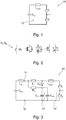
- Fig. 1 is a voltage-driven two-point converter 10 is shown schematically, comprising a Kommut réellesschleife 12 between two semiconductor switches S 1 , S 2 , in which a capacitor C dc is arranged.
- This loop 12 has a leakage inductance or commutation impedance L com .
- the semiconductor switches S 1 , S 2 may comprise, for example, a transistor, thyristor, IGBT, IGCT, RC-IGBT, RC-IGCT, etc.
- Fig. 3 shows a two-point converter 10, which includes further switching components to prevent or at least reduce voltage spikes generated by the leakage inductance L com .
- circuit is a so-called RCLD-damping circuit.
- the components of the converter except the cell capacitor C dc are combined in a common module / stack, wherein the cell capacitor C dc can be connected via terminals 14 and 16 to the module / stack.
- a snubber capacitor C cl1 can be connected in parallel to the cell capacitor C dc and parallel to the series-connected semiconductor switches S 1 , S 2 , which is in spatial proximity to the two semiconductor switches S 1 , S 2 .
- the commutation loop 12 is reduced in size and the inductance of the lines is reduced or the inductance Ls is coupled out of the commutation loop 12.
- a snubber diode D cl and a snubber resistor Rs may be inserted in the commutation loop 12.
- di / dt When the turn-off current or its temporal change is to be controlled di / dt, (for example, between the diode D cl and the semiconductor switches S 1 , S 2 ) and / or if at least a portion of the switching losses of the semiconductor switches S 1 , S 2 in the snubber Resistor Rs is to be performed (for example, for IGBTs as a semiconductor switch S 1 , S 2 ), a di / dt inductor inductance L i can be introduced. The inductance L i can be inserted between the cell capacitor C dc and one of the semiconductor switches S 1 , S 2 .
- one end of the resistor Rs may be connected between the cell capacitor and the inductance L i and / or one end of the diode D cl may be connected between the inductance L i and the semiconductor switch S 1 , S 2 .
- resistor Rs the inductance L i and the diode D cl are not connected to the terminal 14 but to the other terminal 16.
- a snubber capacitor not only a snubber capacitor but a plurality of snubber capacitors C cl1 , C c12 connected in parallel may be used, forming a plurality of commutation loops 12, 12 '.
- the two semiconductor switches S 1 , S 2 and the diode D cl can be arranged together in a stack 18.
- a cooling element 20 or cooling plate 20 is disposed between two semiconductor devices S 1 , S 2 .
- the stack may have a frame 22, with which the components S 1 , S 2 , D cl and 20 can be pressed together. This creates a so-called press pack.
- the diode D cl can also be arranged in an additional stack 24.
- the stack 18 then comprises only the semiconductor switches S 1 , S 2 and the cooling elements 20.
- the stack 18 can be connected to the capacitors C cl1 and C cl2 as well as to the other elements Rs, L i by means of cables, lines and / or bus bars.
- capacitors C cl1 and C c12 and optionally the other components Rs, L i are mechanically connected to the stack 18 and in particular its frame 18.
- capacitors C cl1 and C c12 arranged on the sides of the stack 18 form two parallel commutation loops 12, 12 '.
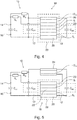
- the Fig. 6 shows a circuit diagram for in the Fig. 7 shown press pack or stack 18, the two series-connected half-bridges 10, 10 'and two-phase converter 10, 10' comprises.
- the semiconductor switches S 1 , S 2 , S 3 and S 4 RC-IGCTs can also be RC-IGBTs or IGBT or IGCT with diodes.
- the semiconductor switches S 1 , S 2 , S 3 and S 4 are connected in series. Also, in the inverter 10, the diode D cl , the inductor L i and the resistor Rs are connected to the upper, first terminal 14, while in the inverter 10 ', these components are connected to the lower second terminal 16. in particular, no additional insulation between the converters 10 and 10 'is necessary.
- the converters 10 and 10 ' can share a heat sink 20 and a cooling box 20, respectively.
- the snubber diode D cl is connected to the semiconductor stack 18 and a mounting bracket 26, respectively.
- the electrically conductive cooling element 20 between the snubber diode D cl and the semiconductor switch S 1 is connected via a conductive connection 28 to an upper, first snubber bus bar 34.
- four snubber capacitors C cl1 , C c12 , C cl1 ', C c12 ' are arranged laterally next to the stack 18 and are connected at an upper end to the first snubber bus bar 34.
- the capacitors C cl1 , C cl1 ' are arranged on one side and the capacitors C c12 , C cl2 ' on the opposite side of the stack 18.
- the capacitors C cl1 , C cl1 ' are connected to a first middle snubber bus bar 36 and the capacitors C c12 , C c12 ' are connected to a second middle bus bar 38.
- the two bus bars 36, 38 are symmetrical to each other and each have a U-shaped bent sheet metal. With the middle part, the two bus bars are connected to an electrically conductive cooling element 20 between the semiconductor switches S 2 and S 4 .
- a lower, second snubber bus bar 40 is connected to the diode D cl of the second inverter 10 '.
- the capacitors C cl1 , C c12 , C cl1 ', C c12 ' of the lower inverter 10 ' are with this diode D cl connected via a bus bar 40 and arranged according to the upper capacitors and connected to the middle busbars 36, 38 accordingly.
Landscapes
- Engineering & Computer Science (AREA)
- Power Engineering (AREA)
- Microelectronics & Electronic Packaging (AREA)
- Physics & Mathematics (AREA)
- Condensed Matter Physics & Semiconductors (AREA)
- General Physics & Mathematics (AREA)
- Computer Hardware Design (AREA)
- Ceramic Engineering (AREA)
- Inverter Devices (AREA)
- Power Conversion In General (AREA)
- Dc-Dc Converters (AREA)
Description
- Die Erfindung betrifft einen Halbleiterstapel bzw. Presspack für einen Leistungsumrichter.
- Bei vielen Leistungselektronik-Schaltungen pendelt bzw. kommutiert der Strom von einem Halbleitergerät zu einem anderen äquivalenten Halbleitergerät über eine Kommutierungsschleife. Beispielsweise umfassen Zweipunktumrichter zwei Halbleiterschalter, die mit einem Kondensator verbunden sind und somit mit dem Kondensator eine Kommutierungsschleife bilden. In der Regel weist die Kommutierungsschleife eine gewisse Streuinduktivität auf, die beispielsweise durch die Leiter, die die Halbleiterbauteile verbinden und die Induktivität des Kondensators erzeugt wird.
- Wenn eine Kommutierung des Stroms zwischen den beiden Schaltern auftritt, fällt der Strom wegen der Streuinduktivität nicht schlagartig ab, sondern ist zeitlich abhängig, was zu Spannungsspitzen führt, die die Halbleiterschalter belasten. Da jeder Halbleiterschalter auch nur eine begrenzte Spannung an seinen Eingängen blockieren kann, reduziert eine hohe Streuinduktivität auch die Leistungsfähigkeit bzw. Schaltgeschwindigkeit des Zweipunktumrichters.
- Beispielsweise kann ein Kondensator mit niedriger Induktivität, wie etwa ein Filmkondensator, gewählt werden um die Streuimpedanz zu senken. Auch können zwischen dem Kondensator und den Halbleiterschaltern Verbindungen mit niedriger Induktivität eingesetzt werden, wie etwa ebene Busschienen, verdrehte Leitungen, usw.
- Auch ist es möglich, einen Snubber-Kondensator (Dämpfungskondensator) räumlich nahe den Halbleiterschaltern anzuordnen, was die Kommutierungsschleife und damit die Streuinduktivität verkleinern kann.
- Leistungs-Halbleiterschalter, die in der Regel flächig ausgeführt sind, werden beispielsweise zusammen mit Kühlelementen in einem Stapel angeordnet und können zu einem sogenannten Presspack verbunden werden. Der Presspack bzw. Stapel kann auch den Snubber-Kondensator umfassen, der seitlich am Presspack bzw. Stapel angeordnet sein kann.
- Die
EP 0 751 612 A2 offenbart eine Stromrichterschaltungsanordnung mit Halbleiterschaltern und Kondensatoren und dieUS 5 045 924 offenbart ein Gehäuse für einen Halbleiterstapel eines Umrichters. - Es ist Aufgabe der Erfindung, einen Halbleiterstapel für einen Umrichter bereitzustellen, der kompakt gebaut ist und der eine niedrige Streuinduktivität in der Kommutierungsschleife aufweist.
- Diese Aufgabe wird durch den Gegenstand des unabhängigen Anspruchs gelöst. Weitere Ausführungsformen der Erfindung ergeben sich aus den abhängigen Ansprüchen und aus der folgenden Beschreibung.
- Die Erfindung betrifft einen Halbleiterstapel für einen Umrichter bzw. eine Halbbrücke, die zusammen mit einem Zellenkondensator einen Umrichter bilden kann. Der Halbleiterstapel kann auch eine unipolare oder bipolare Zelle (in der Regel ohne Zellenkondensator) für einen modularen Multiniveauumrichter umfassen. Unter einem Halbleiterstapel kann dabei ein Stapel von Halbleiterelementen und weiterer Bauelemente, wie etwa Kühlelemente, verstanden werden, die über einem gemeinsamen Rahmen miteinander verbunden sind.
- Gemäß einer Ausführungsform der Erfindung umfasst der Halbleiterstapel zwei in Reihe geschaltete Halbleiterschalter, wie etwa Transistoren, Thyristoren, IGBTs, IGCTs, RC-IGBTs und/oder RC-IGCTs; zwei Anschlüsse zum Anschließen eines Zellenkondensators, die von den beiden Halbleiterschaltern miteinander verbunden werden; wenigstens ein zwischen den Halbleiterschaltern angeordnetes Kühlelement, das beispielsweise elektrisch leitend sein kann und die beiden benachbarten Halbleiterschalter elektrisch verbindet; einen Rahmen, mit dem die Halbleiterschalter und das Kühlelement aneinander fixiert sind und der die Anschlüsse bereitstellt; und wenigstens zwei mechanisch am Rahmen fixierte Snubber-Kondensatoren, die parallel geschaltet sind, mit den Anschlüssen verbunden sind und die jeweils eine Kommutierungsschleife mit den Halbleiterschaltern bilden.
- Auf diese Weise kann ein baulich kompakter Halbleiterstapel bereitgestellt werden, der eine niedrige Streuinduktivität in den Kommutierungsschleifen aufweist. Da parallel geschaltete Induktivitäten zu einer niedrigeren Induktivität führen, führen mehrere (zwei, drei, vier, usw.) Kommutierungsschleifen zu einer Verminderung der Streuinduktivität. Da nicht ein großer, sondern mehrere kleine Kondensatoren um die Halbleiterstapel herum verteilt werden können, kann zusätzlich der Bauraum besser ausgenutzt werden.
- Gemäß einer Ausführungsform der Erfindung umfasst der Halbleiterstapel weiter wenigstens vier mechanisch am Rahmen fixierte Snubber-Kondensatoren. Die Kondensatoren können beispielsweise paarweise seitlich am Halbleiterstapel angebracht werden, beispielsweise über eine gemeinsame Busschiene. Zwei Snubber-Kondensatoren können an gegenüberliegenden Seiten des Halbleiterstapels angeordnet werden. Zwei Snubber-Kondensatoren können alternativ oder zusätzlich räumlich nebeneinander an einer Seite des Halbleiterstapels angeordnet werden.
- Gemäß einer Ausführungsform der Erfindung sind die Snubber-Kondensatoren gleichartig ausgeführt. Die Snubber-Kondensatoren können die gleiche Form, die gleiche Größe und/oder die gleiche Kapazität aufweisen. In der Regel wird ein Snubber-Kondensator einen zylinderförmigen Körper mit elektrischen Kontakten an den Enden aufweisen.
- Gemäß einer Ausführungsform der Erfindung umfasst der Halbleiterstapel weiter eine Snubber-Diode. Die parallel geschalteten Snubber-Kondensatoren können über eine Diode, die Schwingungen bzw. Resonanzen in den Kommutierungsschleifen verhindern kann, mit einem Ende der beiden in Reihe geschalteten Halbleiterschalter verbunden sein.
- Gemäß einer Ausführungsform der Erfindung umfasst der Halbleiterstapel weiter einen Snubber-Widerstand. Die parallel geschalteten Snubber-Kondensatoren können über einen Snubber-Widerstand mit einem Ende der beiden in Reihe geschalteten Halbleiterschalter verbunden sein. Der Snubber-Widerstand kann parallel zu der Snubber-Diode geschaltet sein.
- Gemäß einer Ausführungsform der Erfindung umfasst der Halbleiterstapel weiter eine Drossel-Induktivität. Die Drossel-Induktivität kann zum Einstellen bzw. Steuern der Induktivität der Kommutierungsschleifen und/oder des Leiterkreises zum Zellenkondensator verwendet werden. Beispielsweise kann die Drossel-Induktivität in die Kommutierungsschleifen eingefügt sein und/oder kann den Snubber-Widerstand mit der Snubber-Diode verbinden.
- Gemäß einer Ausführungsform der Erfindung umfasst der Halbleiterstapel weiter ein erstes Paar und ein zweites Paar von in Reihe geschalteten Halbleiterschaltern, die jeweils paarweise mit zwei Zellenkondensatoren verbindbar sind. Der Halbleiterschalter kann zwei in Reihe geschaltete Halbbrücken aufweisen bzw. dazu ausgeführt sein zwei in Reihe geschaltete (Teil-)Umrichter zu bilden.
- Gemäß einer Ausführungsform der Erfindung umfasst der Halbleiterstapel wenigstens zwei mechanisch am Rahmen fixierte erste Snubber-Kondensatoren, die parallel geschaltet sind und die jeweils eine Kommutierungsschleife mit dem ersten Paar von Halbleiterschaltern bilden; und wenigstens zwei mechanisch am Rahmen fixierte zweite Snubber-Kondensatoren, die parallel geschaltet sind und die jeweils eine Kommutierungsschleife mit dem zweiten Paar von Halbleiterschaltern bilden. Der Halbleiterstapel kann für jede der Halbbrücken bzw. Teilumrichter eine Snubber-Schaltung, so wie oben bereits beschrieben, aufweisen. Auch die Komponenten der beiden Snubber-Schaltungen und insbesondere die Snubber-Kondensatoren können seitlich am Halbleiterstapel fixiert sein.
- Gemäß einer Ausführungsform der Erfindung sind die (ersten und/oder zweiten) Snubber-Kondensatoren über eine (erste und/oder zweite) Busschiene miteinander verbunden. Auf diese Weise kann eine Anordnung aus zwei, vier oder mehreren Kondensatoren zueinander fixiert werden. Die (erste und/oder zweite) Busschiene kann am Halbleiterstapel fixiert werden, wodurch die Kondensatoren und damit auch die durch sie bereitgestellten Kommutationsschleifen mechanisch fest mit dem Halbleiterstapel verbunden sind.
- Gemäß einer Ausführungsform der Erfindung sind die ersten Snubber-Kondensatoren mit den zweiten Snubber-Kondensatoren über eine Busschiene miteinander verbunden, die am Halbleiterstapel fixiert sein kann. Diese Busschiene kann beispielsweise direkt an einem elektrisch leitenden, angrenzenden Kühlkörper befestigt sein, der beispielsweise zwischen zwei Halbleiterschaltern im Halbleiterstapel angeordnet ist.
- Mit mehreren Kommutierungsschleifen kann auch der Raum um den Halbleiterstapel besser ausgenutzt werden, da freie Räume dazu genutzt werden können weitere Kondensatoren aufzunehmen.
- Im Folgenden werden Ausführungsbeispiele der Erfindung mit Bezug auf die beiliegenden Figuren detailliert beschrieben.
-
Fig. 1 zeigt ein Schaltdiagramm eines Zweipunktumrichters. -
Fig. 2 zeigt Schaltsymbole für mögliche Halbleiterschalter. -
Fig. 3 zeigt ein Schaltdiagramm für einen Halbleiterstapel gemäß einer Ausführungsform der Erfindung. -
Fig. 4 zeigt schematisch einen Halbleiterstapel gemäß einer Ausführungsform der Erfindung. -
Fig. 5 zeigt schematisch einen Halbleiterstapel gemäß einer weiteren Ausführungsform der Erfindung. -
Fig. 6 zeigt ein Schaltdiagramm für einen Halbleiterstapel gemäß einer weiteren Ausführungsform der Erfindung. -
Fig. 7 zeigt eine dreidimensionale Ansicht eines Halbleiterstapels gemäß einer Ausführungsform der Erfindung. - Die in den Figuren verwendeten Bezugszeichen und ihre Bedeutung sind in zusammenfassender Form in der Liste der Bezugszeichen aufgeführt. Grundsätzlich sind identische oder ähnliche Teile mit den gleichen Bezugszeichen versehen.
- In der
Fig. 1 ist ein spannungsgeführter Zweipunktumrichter 10 schematisch dargestellt, der eine Kommutierungsschleife 12 zwischen zwei Halbleiterschaltern S1, S2 umfasst, in der ein Kondensator Cdc angeordnet ist. Diese Schleife 12 weist eine Streuinduktivität oder Kommutierungsimpedanz Lcom auf. - Wenn eine Kommutierung des Stroms zwischen den beiden Schaltern auftritt, fällt der Strom i wegen der Streuinduktivität nicht schlagartig ab, sondern ist zeitlich abhängig, was zu Spannungsspitzen führt, die die Halbleiterschalter belasten. Die auftretende überspannung v berechnet sich dabei mit v=Lcom *di/dt.
- Wie in der
Fig. 2 dargestellt ist, können die Halbleiterschalter S1, S2 beispielsweise einen Transistor, Thyristor, IGBT, IGCT, RC-IGBT, RC-IGCT etc. umfassen. -
Fig. 3 zeigt einen Zweipunktumrichter 10, der weitere Schaltkomponenten umfasst, um durch die Streuinduktivität Lcom erzeugte Spannungsspitzen zu verhindern oder zumindest zu reduzieren. Bei dem in derFig. 3 gezeigten Schaltkreis handelt es sich um einen sogenannten RCLD-Dämpfungskreis. Beispielsweise sind die Komponenten des Umrichters außer dem Zellkondensator Cdc in einem gemeinsamen Modul/Stapel zusammengefasst, wobei der Zellkondensator Cdc über Anschlüsse 14 und 16 mit dem Modul/Stapel verbunden werden kann. - Zunächst kann ein Snubber-Kondensator Ccl1 parallel zu dem Zellkondensator Cdc und parallel zu den in Reihe geschalteten Halbleiterschaltern S1, S2 geschaltete werden, der sich in räumlicher Nähe zu den beiden Halbleiterschaltern S1, S2 befindet. Auf diese Weise wird die Kommutierungsschleife 12 verkleinert und die Induktivität der Leitungen vermindert bzw. die Induktivität Ls aus der Kommutierungsschleife 12 ausgekoppelt.
- Im Falle ungedämpfter Oszillationen (Resonanzen) zwischen dem Snubber-Kondensator und dem Zell- bzw. Hauptkondensator Cdc, können eine Snubber-Diode (Dämpfungsdiode) Dcl und ein Snubber-Widerstand (Dämpfungswiderstand) Rs in die Kommutierungsschleife 12 eingefügt werden.
- Wenn der Abschaltstrom bzw. dessen zeitliche Änderung di/dt gesteuert werden soll, (beispielsweise zwischen der Diode Dcl und den Halbleiterschaltern S1, S2) und/oder wenn zumindest ein Teil der Schaltverluste der Halbleiterschalter S1, S2 in den Snubber-Widerstand Rs geführt werden soll (beispielsweise für IGBTs als Halbleiterschalter S1, S2), kann eine di/dt-Drossel-Induktivität Li eingeführt werden. Die Induktivität Li kann dabei zwischen den Zellkondensator Cdc und einen der Halbleiterschalter S1, S2 eingefügt werden. Dabei kann ein Ende des Widerstand Rs zwischen den Zellkondensator und die Induktivität Li geschaltet sein und/oder ein Ende der Diode Dcl zwischen die Induktivität Li und den Halbleiterschalter S1, S2.
- Es ist auch möglich, dass der Widerstand Rs, die Induktivität Li und die Diode Dcl nicht mit dem Anschluss 14, sondern mit dem anderen Anschluss 16 verbunden sind.
- Um die Streuinduktivität weiter zu vermindern, können nicht nur ein Snubber-Kondensator sondern eine Mehrzahl von parallel geschalteten Snubber-Kondensatoren Ccl1, Cc12 eingesetzt werden, die eine Mehrzahl von Kommutierungsschleifen 12, 12' bilden.
- Wie in der
Fig. 4 gezeigt ist, können die beiden Halbleiterschalter S1, S2 und die Diode Dcl zusammen in einem Stapel 18 angeordnet werden. Dabei ist zwischen zwei Halbleiterbauelementen S1, S2 jeweils ein Kühlelement 20 bzw. Kühlplatte 20 angeordnet. - Der Stapel kann einen Rahmen 22 aufweisen, mit dem die Bauelemente S1, S2, Dcl und 20 zusammengepresst werden können. Auf diese Weise entsteht ein sogenannter Presspack.
- Wie in der
Fig. 5 gezeigt ist, kann die Diode Dcl auch in einem zusätzlichen Stapel 24 angeordnet werden. Der Stapel 18 umfasst dann lediglich die Halbleiterschalter S1, S2 und die Kühlelemente 20. - Der Stapel 18 kann mit den Kondensatoren Ccl1 und Ccl2 sowie mit den anderen Elementen Rs, Li mittels Kabeln, Leitungen und/oder Busschienen verbunden werden.
- Weiter sind die Kondensatoren Ccl1 und Cc12 sowie optional die anderen Bauelemente Rs, Li mit dem Stapel 18 und insbesondere dessen Rahmen 18 mechanisch verbunden.
- Insbesondere formen die an den Seiten des Stapels 18 angeordneten Kondensatoren Ccl1 und Cc12 zwei parallele Kommutationsschleifen 12, 12'.
- Die
Fig. 6 zeigt ein Schaltdiagramm für den in derFig. 7 gezeigten Presspack bzw. Stapel 18, der zwei in Reihe geschaltete Halbbrücken 10, 10' bzw. Zweipunktumrichter 10, 10' umfasst. Im dargestellten Beispiel sind die Halbleiterschalter S1, S2, S3 und S4 RC-IGCTs, können aber auch RC-IGBTs oder IGBT bzw. IGCT mit Dioden sein. - Die Halbleiterschalter S1, S2, S3 und S4 sind in Reihe geschaltet. Auch sind bei dem Umrichter 10, die Diode Dcl, die Drossel Li und der Widerstand Rs mit dem oberen, ersten Anschluss 14 verbunden, während bei dem Umrichter 10' diese Komponenten mit dem unteren, zweiten Anschluss 16 verbunden sind. es ist insbesondere keine zusätzliche Isolation zwischen den Umrichtern 10 und 10' notwendig. Die Umrichter 10 und 10' können einen Kühlkörper 20 bzw. eine Kühldose 20 gemeinsam nutzen.
- In der
Fig. 7 sind lediglich die in derFig. 6 umrahmten Komponenten dargestellt. Die Snubber-Diode Dcl ist mit dem Halbleiterstapel 18 bzw. einer Montierklammer 26 verbunden. Das elektrisch leitende Kühlelement 20 zwischen der Snubber-Diode Dcl und dem Halbleiterschalter S1 ist über eine leitende Verbindung 28 mit einer oberen, ersten Snubber-Busschiene 34 verbunden. Räumlich parallel zu dem Stapel 18 sind seitlich neben dem Stapel 18 vier Snubber-Kondensatoren Ccl1, Cc12, Ccl1', Cc12' angeordnet, die an einem oberen Ende mit der ersten Snubber-Busschiene 34 verbunden sind. - Die Kondensatoren Ccl1, Ccl1' sind dabei an einer Seite und die Kondensatoren Cc12, Ccl2' an der gegenüberliegenden Seite des Stapels 18 angeordnet.
- An ihrem unteren Ende sind die Kondensatoren Ccl1, Ccl1' mit einer ersten mittleren Snubber-Busschiene 36 und die Kondensatoren Cc12, Cc12' mit einer zweiten mittleren Busschiene 38 verbunden. Die beiden Busschienen 36, 38 sind symmetrisch zueinander aufgebaut und weisen jeweils ein U-förmig gebogenes Blech auf. Mit dem Mittelteil sind die beiden Busschienen mit einem elektrisch leitenden Kühlelement 20 zwischen den Halbleiterschaltern S2 und S4 verbunden.
- Eine untere, zweite Snubber-Busschiene 40 ist mit der Diode Dcl des zweiten Umrichters 10' verbunden. Die Kondensatoren Ccl1, Cc12, Ccl1', Cc12' des unteren Umrichters 10' sind mit dieser Diode Dcl über eine Busschiene 40 verbunden und den oberen Kondensatoren entsprechend angeordnet sowie entsprechend mit den mittleren Busschienen 36, 38 verbunden.
- Für jeden der Umrichter 10, 10' sind in der
Fig. 7 vier Kommutierungsschleifen zu erkennen. -
- 10, 10'
- Zweipunktumrichter
- 12, 12'
- Kommutierungsschleife
- S1, S2
- Halbleiterschalter
- Cdc
- Zellkondensator
- Lcom, LS
- Streuinduktivität
- Ccl1, Ccl2
- Snubber-Kondensator
- Dcl
- Snubber-Diode
- RS
- Snubber-Widerstand
- Li
- Drossel-Induktivität
- 14, 16
- Anschluss
- 18
- Halbleiterstapel
- 20
- Kühlelement
- 22
- Rahmen
- 24
- Hilfsstapel
- S3, S4
- Halbleiterschalter
- 26
- mechanische Montierklammer
- 28
- elektrische Verbindung
- 34
- obere, erste Snubber-Busschiene
- 36, 38
- mittlere Snubber-Busschiene
- 40
- untere, zweite Snubber-Busschiene
Claims (9)
- Halbleiterstapel (18) für einen Umrichter (10), der Halbleiterstapel (18) umfassend:zwei in Reihe geschaltete Halbleiterschalter (S1, S2);zwei Anschlüsse (14, 16) zum Anschließen eines Zellenkondensators (Cdc), die von den beiden Halbleiterschaltern (S1, S2) miteinander verbunden werden;wenigstens ein zwischen den Halbleiterschaltern (S1, S2) angeordnetes Kühlelement (20);einen Rahmen (22), mit dem die Halbleiterschalter (S1, S2) und das Kühlelement (20) aneinander fixiert sind und der die Anschlüsse bereitstellt; undwenigstens zwei mechanisch am Rahmen (22) fixierte Snubber-Kondensatoren (Ccl1, Ccl2), die parallel geschaltet sind, mit den Anschlüssen verbunden sind und die jeweils eine Kommutierungsschleife (12, 12') mit den beiden Halbleiterschaltern (S1, S2) bilden.
- Halbleiterstapel (18) nach Anspruch 1, weiter umfassend:wenigstens vier mechanisch am Rahmen (22) fixierte Snubber-Kondensatoren (Ccl1, Ccl2, Ccl1', Ccl2').
- Halbleiterstapel (18) nach Anspruch 1 oder 2,
wobei zwei Snubber-Kondensatoren (Ccl1, Cc12) an gegenüberliegenden Seiten des Halbleiterstapels angeordnet sind. - Halbleiterstapel (18) nach einem der vorhergehenden Ansprüche,
wobei zwei Snubber-Kondensatoren (Ccl1, Ccl1') räumlich nebeneinander an einer Seite des Halbleiterstapels angeordnet sind. - Halbleiterstapel (18) nach einem der vorhergehenden Ansprüche,
wobei die Snubber-Kondensatoren (Ccl1, Cc12, Ccl1', Ccl2') gleichartig ausgeführt sind. - Halbleiterstapel (18) nach einem der vorhergehenden Ansprüche, weiter umfassend:eine Snubber-Diode (Dcl) ; und/odereinen Snubber-Widerstand (Rs) und/odereine Drossel-Induktivität (Li).
- Halbleiterstapel (18) nach einem der vorhergehenden Ansprüche, weiter umfassend:ein erstes Paar (S1, S2) und ein zweites Paar (S3, S4) von in Reihe geschalteten Halbleiterschaltern, die jeweils paarweise mit zwei Zellenkondensatoren (Cdc) verbindbar sind;wenigstens zwei mechanisch am Rahmen (22) fixierte erste Snubber-Kondensatoren (Ccl1, Cc12, Ccl1', Ccl2'), die parallel geschaltet sind und die jeweils eine Kommutierungsschleife mit dem ersten Paar (S1, S2) von Halbleiterschaltern bilden; undwenigstens zwei mechanisch am Rahmen (22) fixierte zweite Snubber-Kondensatoren (Ccl1, Cc12, Ccl1', Ccl2'), die parallel geschaltet sind und die jeweils eine Kommutierungsschleife mit dem zweiten Paar (S3, S4) von Halbleiterschaltern bilden.
- Halbleiterstapel (18) nach einem der Ansprüche 7,
wobei die ersten Snubber-Kondensatoren (Ccl1, Cc12, Ccl1', Cc12') über eine erste Busschiene (34) miteinander verbunden sind, die zweiten Snubber-Kondensatoren (Ccl1, Cc12, Ccl1', Ccl2') über eine zweite Busschiene (40) miteinander verbunden sind und die ersten Snubber-Kondensatoren mit den zweiten Snubber-Kondensatoren über eine Busschiene (36, 38) miteinander verbunden sind, wobei die Busschiene (36, 38) an einem Kühlkörper (20) zwischen den Paaren von Halbleiterschaltern fixiert ist. - Halbleiterstapel (18) nach einem der vorhergehenden Ansprüche,
wobei die Halbleiterschalter (S1, S2, S3, S4) ausgewählt sind aus: Transistoren, Thyristoren, IGBTs, IGCTs, RC-IGBTs und/oder RC-IGCTs.
Applications Claiming Priority (2)
| Application Number | Priority Date | Filing Date | Title |
|---|---|---|---|
| DE202013104510U DE202013104510U1 (de) | 2013-10-04 | 2013-10-04 | Halbleiterstapel für Umrichter mit Snubber-Kondensatoren |
| PCT/EP2014/071296 WO2015049387A1 (de) | 2013-10-04 | 2014-10-06 | Halbleiterstapel für umrichter mit snubber-kondensatoren |
Publications (2)
| Publication Number | Publication Date |
|---|---|
| EP2989660A1 EP2989660A1 (de) | 2016-03-02 |
| EP2989660B1 true EP2989660B1 (de) | 2017-01-04 |
Family
ID=49781040
Family Applications (1)
| Application Number | Title | Priority Date | Filing Date |
|---|---|---|---|
| EP14780861.2A Active EP2989660B1 (de) | 2013-10-04 | 2014-10-06 | Halbleiterstapel für umrichter mit snubber-kondensatoren |
Country Status (9)
| Country | Link |
|---|---|
| US (1) | US10164519B2 (de) |
| EP (1) | EP2989660B1 (de) |
| CN (1) | CN105593989B (de) |
| AU (1) | AU2014331067A1 (de) |
| BR (1) | BR112016006798A2 (de) |
| CA (1) | CA2926022A1 (de) |
| DE (1) | DE202013104510U1 (de) |
| MX (1) | MX2016004075A (de) |
| WO (1) | WO2015049387A1 (de) |
Families Citing this family (6)
| Publication number | Priority date | Publication date | Assignee | Title |
|---|---|---|---|---|
| DE102014209690B4 (de) | 2014-05-21 | 2020-02-20 | Robert Bosch Gmbh | Kommutierungszelle |
| FR3043284B1 (fr) * | 2015-10-29 | 2023-06-23 | Ifp Energies Now | Systeme de conversion d'une puissance electrique continue en puissance electrique alternative avec module recuperateur d'energie |
| WO2018006970A1 (en) * | 2016-07-07 | 2018-01-11 | Abb Schweiz Ag | Semiconductor power stack of a modular multilevel converter |
| DE102017203420A1 (de) * | 2017-03-02 | 2018-09-06 | Siemens Aktiengesellschaft | Halbbrücke für leistungselektronische Schaltungen |
| US11646653B2 (en) | 2019-10-15 | 2023-05-09 | Hitachi Energy Switzerland Ag | Switching circuit with snubber components |
| EP4429098A1 (de) * | 2023-03-10 | 2024-09-11 | GE Energy Power Conversion Technology Ltd | Submodul und zugehöriges modul, turm, stromrichter und stromversorgungssystem |
Family Cites Families (26)
| Publication number | Priority date | Publication date | Assignee | Title |
|---|---|---|---|---|
| JPS589349A (ja) * | 1981-07-10 | 1983-01-19 | Hitachi Ltd | Gtoスタツク |
| US4674024A (en) * | 1986-06-05 | 1987-06-16 | Westinghouse Electric Corp. | High voltage modular inverter and control system thereof |
| FI880817A (fi) * | 1987-07-17 | 1989-01-18 | Siemens Ag | Anordning foer koppling med laog foerlust av ett halvledarkopplingselement i en trepunktvaexelriktare. |
| DE3743436C1 (de) * | 1987-12-21 | 1989-05-11 | Siemens Ag | Schaltentlasteter,verlustarmer Dreipunktwechselrichter |
| US5045924A (en) * | 1988-02-26 | 1991-09-03 | Kabushiki Kaisha Toshiba | Mounting structure of semiconductor converter |
| JP2658427B2 (ja) * | 1989-01-17 | 1997-09-30 | 富士電機株式会社 | 電力変換用半導体素子のスナバ回路とそのモジュール装置 |
| JP3325030B2 (ja) * | 1991-06-06 | 2002-09-17 | 三菱電機株式会社 | 3レベルインバータ装置 |
| EP0838855B1 (de) | 1991-09-20 | 2004-11-24 | Hitachi, Ltd. | Halbleitermodul |
| JP3173068B2 (ja) * | 1991-10-22 | 2001-06-04 | 株式会社日立製作所 | 電力変換器 |
| JP2735497B2 (ja) * | 1995-01-31 | 1998-04-02 | 株式会社東芝 | スナバ回路 |
| DE19523095A1 (de) * | 1995-06-26 | 1997-01-02 | Abb Management Ag | Stromrichterschaltungsanordnung |
| US6169672B1 (en) * | 1996-07-03 | 2001-01-02 | Hitachi, Ltd. | Power converter with clamping circuit |
| DE19632173A1 (de) * | 1996-08-09 | 1998-02-12 | Asea Brown Boveri | Stromrichterschaltungsanordnung |
| US5982646A (en) * | 1998-06-30 | 1999-11-09 | General Electric Company | Voltage clamp snubbers for three level converter |
| JP2001057407A (ja) | 1999-08-19 | 2001-02-27 | Meidensha Corp | ヒートシンク配置装置 |
| JP3652934B2 (ja) * | 1999-09-06 | 2005-05-25 | 東芝三菱電機産業システム株式会社 | 電力変換装置 |
| DE10062075A1 (de) * | 2000-12-13 | 2002-06-27 | Bosch Gmbh Robert | Umrichter mit integrierten Zwischenkreiskondensatoren |
| WO2003017452A2 (en) * | 2001-08-13 | 2003-02-27 | Inductotherm Corp. | Fault tolerant power supply circuit |
| EP1768244A1 (de) * | 2004-07-01 | 2007-03-28 | The Kansai Electric Power Co., Inc. | Snubber-schaltung und leistungshalbleitereinrichtung mit snubber-schaltung |
| JP4661645B2 (ja) | 2005-03-23 | 2011-03-30 | トヨタ自動車株式会社 | パワー半導体モジュール |
| EP2266137B1 (de) * | 2008-03-20 | 2018-06-13 | ABB Schweiz AG | U-umrichter |
| US8385068B2 (en) * | 2009-06-16 | 2013-02-26 | Abb Technology Ag | Cooling of electrical components |
| JP5218541B2 (ja) | 2010-12-14 | 2013-06-26 | 株式会社デンソー | スイッチングモジュール |
| FR2976404B1 (fr) * | 2011-06-10 | 2013-07-12 | Converteam Technology Ltd | Pile de composants electroniques maintenus suivant un empilement presse |
| WO2013009711A1 (en) * | 2011-07-08 | 2013-01-17 | Timler John P | Insulator based upon one or more dielectric structures |
| DE202012008739U1 (de) | 2012-09-12 | 2013-12-16 | Abb Technology Ag | Kühlkreislauf mit ausreichend knapp bemessenem Wärmetauscher |
-
2013
- 2013-10-04 DE DE202013104510U patent/DE202013104510U1/de not_active Expired - Lifetime
-
2014
- 2014-10-06 AU AU2014331067A patent/AU2014331067A1/en not_active Abandoned
- 2014-10-06 MX MX2016004075A patent/MX2016004075A/es unknown
- 2014-10-06 CN CN201480054633.9A patent/CN105593989B/zh active Active
- 2014-10-06 CA CA2926022A patent/CA2926022A1/en not_active Abandoned
- 2014-10-06 WO PCT/EP2014/071296 patent/WO2015049387A1/de active Application Filing
- 2014-10-06 EP EP14780861.2A patent/EP2989660B1/de active Active
- 2014-10-06 BR BR112016006798A patent/BR112016006798A2/pt not_active IP Right Cessation
-
2016
- 2016-04-01 US US15/088,812 patent/US10164519B2/en active Active
Also Published As
| Publication number | Publication date |
|---|---|
| MX2016004075A (es) | 2016-08-11 |
| AU2014331067A1 (en) | 2016-05-05 |
| DE202013104510U1 (de) | 2013-11-14 |
| CN105593989A (zh) | 2016-05-18 |
| CN105593989B (zh) | 2019-12-24 |
| US10164519B2 (en) | 2018-12-25 |
| CA2926022A1 (en) | 2015-04-09 |
| BR112016006798A2 (pt) | 2017-08-01 |
| EP2989660A1 (de) | 2016-03-02 |
| WO2015049387A1 (de) | 2015-04-09 |
| US20160218615A1 (en) | 2016-07-28 |
Similar Documents
| Publication | Publication Date | Title |
|---|---|---|
| EP2989660B1 (de) | Halbleiterstapel für umrichter mit snubber-kondensatoren | |
| DE19732402B4 (de) | Elektrische Busanordnung zur Gleichstromversorgung von Schaltungselementen eines Wechselrichters | |
| DE102018106357A1 (de) | Leistungsumwandlungsgerät | |
| WO2017174102A1 (de) | Modul für einen multilevelkonverter | |
| EP2996449B1 (de) | Stromrichteranordnung mit einem mehrphasigen Stromrichter | |
| DE4110339A1 (de) | Wechselrichtereinheit mit verbesserter stromleiterplattenkonfiguration | |
| DE102010002627A1 (de) | Niederinduktive Leistungshalbleiterbaugruppe | |
| EP2524431A1 (de) | Schaltungsanordnung von elektronischen leistungsschaltern einer stromerzeugungsvorrichtung | |
| EP3404818B1 (de) | Halbleiterschaltanordnung | |
| EP1670131A2 (de) | Leistungshalbleitermodul mit verringerten parasitären Induktivitäten | |
| DE102018200712A1 (de) | Wandlervorrichtung elektrischer Leistung, Solarenergie-Aufbereitungssystem, Stromspeichersystem, unterbrechungsfreies Leistungsversorgungssystem, Windenergieerzeugungssystem und Motorantriebssystem | |
| DE202015004662U1 (de) | Zwischenkreiskondensatormodul mit niederinduktiven Busbar-Verbindungen | |
| EP3180850B1 (de) | Niederinduktive schaltungsanordnung eines umrichters | |
| EP3098958B1 (de) | Spannungswandleranordnung mit kapazitiver kopplung | |
| DE102013104522B3 (de) | Leistungshalbleitermodul mit Subeinheiten und Anordnung hiermit | |
| EP2564501B1 (de) | Submodul für einen modularen mehrstufenumrichter | |
| EP3304718B1 (de) | Gleichspannungswandler für hohe spannungen | |
| DE102014111438B4 (de) | Leistungsbaustein und Verfahren zu dessen Herstellung | |
| WO2020078967A1 (de) | Wechselrichtereinrichtung mit halbbrückenmodul | |
| WO2001039347A1 (de) | Schutzvorrichtung gegen die durch schaltvorgänge verursachten überspannungen an klemmen eines elektrischen betriebsmittels | |
| DE102015105889A1 (de) | Schaltmodul und Umrichter mit wenigstens einem Schaltmodul | |
| WO2002069482A1 (de) | Schaltungsaufbau für eine schaltung zum schalten von strömen | |
| WO2018113926A1 (de) | Stromrichter | |
| EP3571758B1 (de) | Modularer wechselrichter | |
| DE102013102707A1 (de) | Wechselrichter mit mindestens einer Wechselrichterbrücke zwischen zwei Busbars |
Legal Events
| Date | Code | Title | Description |
|---|---|---|---|
| PUAI | Public reference made under article 153(3) epc to a published international application that has entered the european phase |
Free format text: ORIGINAL CODE: 0009012 |
|
| 17P | Request for examination filed |
Effective date: 20151127 |
|
| AK | Designated contracting states |
Kind code of ref document: A1 Designated state(s): AL AT BE BG CH CY CZ DE DK EE ES FI FR GB GR HR HU IE IS IT LI LT LU LV MC MK MT NL NO PL PT RO RS SE SI SK SM TR |
|
| AX | Request for extension of the european patent |
Extension state: BA ME |
|
| GRAP | Despatch of communication of intention to grant a patent |
Free format text: ORIGINAL CODE: EPIDOSNIGR1 |
|
| INTG | Intention to grant announced |
Effective date: 20160623 |
|
| GRAS | Grant fee paid |
Free format text: ORIGINAL CODE: EPIDOSNIGR3 |
|
| RAP1 | Party data changed (applicant data changed or rights of an application transferred) |
Owner name: ABB SCHWEIZ AG |
|
| GRAA | (expected) grant |
Free format text: ORIGINAL CODE: 0009210 |
|
| DAX | Request for extension of the european patent (deleted) | ||
| AK | Designated contracting states |
Kind code of ref document: B1 Designated state(s): AL AT BE BG CH CY CZ DE DK EE ES FI FR GB GR HR HU IE IS IT LI LT LU LV MC MK MT NL NO PL PT RO RS SE SI SK SM TR |
|
| REG | Reference to a national code |
Ref country code: GB Ref legal event code: FG4D Free format text: NOT ENGLISH |
|
| REG | Reference to a national code |
Ref country code: CH Ref legal event code: EP |
|
| REG | Reference to a national code |
Ref country code: AT Ref legal event code: REF Ref document number: 860001 Country of ref document: AT Kind code of ref document: T Effective date: 20170115 |
|
| REG | Reference to a national code |
Ref country code: IE Ref legal event code: FG4D Free format text: LANGUAGE OF EP DOCUMENT: GERMAN |
|
| REG | Reference to a national code |
Ref country code: DE Ref legal event code: R096 Ref document number: 502014002422 Country of ref document: DE |
|
| REG | Reference to a national code |
Ref country code: LT Ref legal event code: MG4D Ref country code: NL Ref legal event code: MP Effective date: 20170104 |
|
| PG25 | Lapsed in a contracting state [announced via postgrant information from national office to epo] |
Ref country code: NL Free format text: LAPSE BECAUSE OF FAILURE TO SUBMIT A TRANSLATION OF THE DESCRIPTION OR TO PAY THE FEE WITHIN THE PRESCRIBED TIME-LIMIT Effective date: 20170104 |
|
| PG25 | Lapsed in a contracting state [announced via postgrant information from national office to epo] |
Ref country code: FI Free format text: LAPSE BECAUSE OF FAILURE TO SUBMIT A TRANSLATION OF THE DESCRIPTION OR TO PAY THE FEE WITHIN THE PRESCRIBED TIME-LIMIT Effective date: 20170104 Ref country code: NO Free format text: LAPSE BECAUSE OF FAILURE TO SUBMIT A TRANSLATION OF THE DESCRIPTION OR TO PAY THE FEE WITHIN THE PRESCRIBED TIME-LIMIT Effective date: 20170404 Ref country code: GR Free format text: LAPSE BECAUSE OF FAILURE TO SUBMIT A TRANSLATION OF THE DESCRIPTION OR TO PAY THE FEE WITHIN THE PRESCRIBED TIME-LIMIT Effective date: 20170405 Ref country code: HR Free format text: LAPSE BECAUSE OF FAILURE TO SUBMIT A TRANSLATION OF THE DESCRIPTION OR TO PAY THE FEE WITHIN THE PRESCRIBED TIME-LIMIT Effective date: 20170104 Ref country code: LT Free format text: LAPSE BECAUSE OF FAILURE TO SUBMIT A TRANSLATION OF THE DESCRIPTION OR TO PAY THE FEE WITHIN THE PRESCRIBED TIME-LIMIT Effective date: 20170104 Ref country code: IS Free format text: LAPSE BECAUSE OF FAILURE TO SUBMIT A TRANSLATION OF THE DESCRIPTION OR TO PAY THE FEE WITHIN THE PRESCRIBED TIME-LIMIT Effective date: 20170504 |
|
| PG25 | Lapsed in a contracting state [announced via postgrant information from national office to epo] |
Ref country code: LV Free format text: LAPSE BECAUSE OF FAILURE TO SUBMIT A TRANSLATION OF THE DESCRIPTION OR TO PAY THE FEE WITHIN THE PRESCRIBED TIME-LIMIT Effective date: 20170104 Ref country code: BG Free format text: LAPSE BECAUSE OF FAILURE TO SUBMIT A TRANSLATION OF THE DESCRIPTION OR TO PAY THE FEE WITHIN THE PRESCRIBED TIME-LIMIT Effective date: 20170404 Ref country code: PL Free format text: LAPSE BECAUSE OF FAILURE TO SUBMIT A TRANSLATION OF THE DESCRIPTION OR TO PAY THE FEE WITHIN THE PRESCRIBED TIME-LIMIT Effective date: 20170104 Ref country code: RS Free format text: LAPSE BECAUSE OF FAILURE TO SUBMIT A TRANSLATION OF THE DESCRIPTION OR TO PAY THE FEE WITHIN THE PRESCRIBED TIME-LIMIT Effective date: 20170104 Ref country code: PT Free format text: LAPSE BECAUSE OF FAILURE TO SUBMIT A TRANSLATION OF THE DESCRIPTION OR TO PAY THE FEE WITHIN THE PRESCRIBED TIME-LIMIT Effective date: 20170504 Ref country code: SE Free format text: LAPSE BECAUSE OF FAILURE TO SUBMIT A TRANSLATION OF THE DESCRIPTION OR TO PAY THE FEE WITHIN THE PRESCRIBED TIME-LIMIT Effective date: 20170104 Ref country code: ES Free format text: LAPSE BECAUSE OF FAILURE TO SUBMIT A TRANSLATION OF THE DESCRIPTION OR TO PAY THE FEE WITHIN THE PRESCRIBED TIME-LIMIT Effective date: 20170104 |
|
| REG | Reference to a national code |
Ref country code: DE Ref legal event code: R097 Ref document number: 502014002422 Country of ref document: DE |
|
| REG | Reference to a national code |
Ref country code: FR Ref legal event code: PLFP Year of fee payment: 4 |
|
| PG25 | Lapsed in a contracting state [announced via postgrant information from national office to epo] |
Ref country code: IT Free format text: LAPSE BECAUSE OF FAILURE TO SUBMIT A TRANSLATION OF THE DESCRIPTION OR TO PAY THE FEE WITHIN THE PRESCRIBED TIME-LIMIT Effective date: 20170104 Ref country code: EE Free format text: LAPSE BECAUSE OF FAILURE TO SUBMIT A TRANSLATION OF THE DESCRIPTION OR TO PAY THE FEE WITHIN THE PRESCRIBED TIME-LIMIT Effective date: 20170104 Ref country code: SK Free format text: LAPSE BECAUSE OF FAILURE TO SUBMIT A TRANSLATION OF THE DESCRIPTION OR TO PAY THE FEE WITHIN THE PRESCRIBED TIME-LIMIT Effective date: 20170104 Ref country code: RO Free format text: LAPSE BECAUSE OF FAILURE TO SUBMIT A TRANSLATION OF THE DESCRIPTION OR TO PAY THE FEE WITHIN THE PRESCRIBED TIME-LIMIT Effective date: 20170104 Ref country code: CZ Free format text: LAPSE BECAUSE OF FAILURE TO SUBMIT A TRANSLATION OF THE DESCRIPTION OR TO PAY THE FEE WITHIN THE PRESCRIBED TIME-LIMIT Effective date: 20170104 |
|
| PLBE | No opposition filed within time limit |
Free format text: ORIGINAL CODE: 0009261 |
|
| STAA | Information on the status of an ep patent application or granted ep patent |
Free format text: STATUS: NO OPPOSITION FILED WITHIN TIME LIMIT |
|
| PG25 | Lapsed in a contracting state [announced via postgrant information from national office to epo] |
Ref country code: DK Free format text: LAPSE BECAUSE OF FAILURE TO SUBMIT A TRANSLATION OF THE DESCRIPTION OR TO PAY THE FEE WITHIN THE PRESCRIBED TIME-LIMIT Effective date: 20170104 Ref country code: SM Free format text: LAPSE BECAUSE OF FAILURE TO SUBMIT A TRANSLATION OF THE DESCRIPTION OR TO PAY THE FEE WITHIN THE PRESCRIBED TIME-LIMIT Effective date: 20170104 |
|
| PG25 | Lapsed in a contracting state [announced via postgrant information from national office to epo] |
Ref country code: SI Free format text: LAPSE BECAUSE OF FAILURE TO SUBMIT A TRANSLATION OF THE DESCRIPTION OR TO PAY THE FEE WITHIN THE PRESCRIBED TIME-LIMIT Effective date: 20170104 |
|
| PG25 | Lapsed in a contracting state [announced via postgrant information from national office to epo] |
Ref country code: MC Free format text: LAPSE BECAUSE OF FAILURE TO SUBMIT A TRANSLATION OF THE DESCRIPTION OR TO PAY THE FEE WITHIN THE PRESCRIBED TIME-LIMIT Effective date: 20170104 |
|
| REG | Reference to a national code |
Ref country code: IE Ref legal event code: MM4A |
|
| PG25 | Lapsed in a contracting state [announced via postgrant information from national office to epo] |
Ref country code: LU Free format text: LAPSE BECAUSE OF NON-PAYMENT OF DUE FEES Effective date: 20171006 |
|
| REG | Reference to a national code |
Ref country code: BE Ref legal event code: MM Effective date: 20171031 |
|
| PG25 | Lapsed in a contracting state [announced via postgrant information from national office to epo] |
Ref country code: BE Free format text: LAPSE BECAUSE OF NON-PAYMENT OF DUE FEES Effective date: 20171031 |
|
| PG25 | Lapsed in a contracting state [announced via postgrant information from national office to epo] |
Ref country code: MT Free format text: LAPSE BECAUSE OF FAILURE TO SUBMIT A TRANSLATION OF THE DESCRIPTION OR TO PAY THE FEE WITHIN THE PRESCRIBED TIME-LIMIT Effective date: 20170104 |
|
| REG | Reference to a national code |
Ref country code: FR Ref legal event code: PLFP Year of fee payment: 5 |
|
| PG25 | Lapsed in a contracting state [announced via postgrant information from national office to epo] |
Ref country code: IE Free format text: LAPSE BECAUSE OF NON-PAYMENT OF DUE FEES Effective date: 20171006 |
|
| PG25 | Lapsed in a contracting state [announced via postgrant information from national office to epo] |
Ref country code: HU Free format text: LAPSE BECAUSE OF FAILURE TO SUBMIT A TRANSLATION OF THE DESCRIPTION OR TO PAY THE FEE WITHIN THE PRESCRIBED TIME-LIMIT; INVALID AB INITIO Effective date: 20141006 |
|
| PG25 | Lapsed in a contracting state [announced via postgrant information from national office to epo] |
Ref country code: CY Free format text: LAPSE BECAUSE OF FAILURE TO SUBMIT A TRANSLATION OF THE DESCRIPTION OR TO PAY THE FEE WITHIN THE PRESCRIBED TIME-LIMIT Effective date: 20170104 |
|
| PG25 | Lapsed in a contracting state [announced via postgrant information from national office to epo] |
Ref country code: MK Free format text: LAPSE BECAUSE OF FAILURE TO SUBMIT A TRANSLATION OF THE DESCRIPTION OR TO PAY THE FEE WITHIN THE PRESCRIBED TIME-LIMIT Effective date: 20170104 |
|
| PG25 | Lapsed in a contracting state [announced via postgrant information from national office to epo] |
Ref country code: TR Free format text: LAPSE BECAUSE OF FAILURE TO SUBMIT A TRANSLATION OF THE DESCRIPTION OR TO PAY THE FEE WITHIN THE PRESCRIBED TIME-LIMIT Effective date: 20170104 |
|
| PG25 | Lapsed in a contracting state [announced via postgrant information from national office to epo] |
Ref country code: AL Free format text: LAPSE BECAUSE OF FAILURE TO SUBMIT A TRANSLATION OF THE DESCRIPTION OR TO PAY THE FEE WITHIN THE PRESCRIBED TIME-LIMIT Effective date: 20170104 |
|
| REG | Reference to a national code |
Ref country code: CH Ref legal event code: NV Representative=s name: DENNEMEYER AG, CH Ref country code: CH Ref legal event code: PUE Owner name: ABB POWER GRIDS SWITZERLAND AG, CH Free format text: FORMER OWNER: ABB SCHWEIZ AG, CH |
|
| REG | Reference to a national code |
Ref country code: DE Ref legal event code: R081 Ref document number: 502014002422 Country of ref document: DE Owner name: HITACHI ENERGY SWITZERLAND AG, CH Free format text: FORMER OWNER: ABB SCHWEIZ AG, BADEN, CH Ref country code: DE Ref legal event code: R081 Ref document number: 502014002422 Country of ref document: DE Owner name: HITACHI ENERGY LTD, CH Free format text: FORMER OWNER: ABB SCHWEIZ AG, BADEN, CH Ref country code: DE Ref legal event code: R082 Ref document number: 502014002422 Country of ref document: DE Representative=s name: DENNEMEYER & ASSOCIATES S.A., DE Ref country code: DE Ref legal event code: R081 Ref document number: 502014002422 Country of ref document: DE Owner name: ABB POWER GRIDS SWITZERLAND AG, CH Free format text: FORMER OWNER: ABB SCHWEIZ AG, BADEN, CH |
|
| REG | Reference to a national code |
Ref country code: AT Ref legal event code: PC Ref document number: 860001 Country of ref document: AT Kind code of ref document: T Owner name: ABB POWER GRIDS SWITZERLAND AG, CH Effective date: 20210708 |
|
| REG | Reference to a national code |
Ref country code: GB Ref legal event code: 732E Free format text: REGISTERED BETWEEN 20220421 AND 20220427 |
|
| REG | Reference to a national code |
Ref country code: DE Ref legal event code: R081 Ref document number: 502014002422 Country of ref document: DE Owner name: HITACHI ENERGY SWITZERLAND AG, CH Free format text: FORMER OWNER: ABB POWER GRIDS SWITZERLAND AG, BADEN, CH Ref country code: DE Ref legal event code: R081 Ref document number: 502014002422 Country of ref document: DE Owner name: HITACHI ENERGY LTD, CH Free format text: FORMER OWNER: ABB POWER GRIDS SWITZERLAND AG, BADEN, CH |
|
| REG | Reference to a national code |
Ref country code: AT Ref legal event code: HC Ref document number: 860001 Country of ref document: AT Kind code of ref document: T Owner name: HITACHI ENERGY SWITZERLAND AG, CH Effective date: 20220718 |
|
| P01 | Opt-out of the competence of the unified patent court (upc) registered |
Effective date: 20230527 |
|
| PGFP | Annual fee paid to national office [announced via postgrant information from national office to epo] |
Ref country code: GB Payment date: 20231020 Year of fee payment: 10 |
|
| PGFP | Annual fee paid to national office [announced via postgrant information from national office to epo] |
Ref country code: FR Payment date: 20231026 Year of fee payment: 10 Ref country code: DE Payment date: 20231020 Year of fee payment: 10 Ref country code: CH Payment date: 20231101 Year of fee payment: 10 Ref country code: AT Payment date: 20231020 Year of fee payment: 10 |
|
| REG | Reference to a national code |
Ref country code: DE Ref legal event code: R082 Ref document number: 502014002422 Country of ref document: DE Representative=s name: DENNEMEYER & ASSOCIATES S.A., DE Ref country code: DE Ref legal event code: R081 Ref document number: 502014002422 Country of ref document: DE Owner name: HITACHI ENERGY LTD, CH Free format text: FORMER OWNER: HITACHI ENERGY SWITZERLAND AG, BADEN, CH |
|
| REG | Reference to a national code |
Ref country code: AT Ref legal event code: PC Ref document number: 860001 Country of ref document: AT Kind code of ref document: T Owner name: HITACHI ENERGY LTD, CH Effective date: 20240416 |
|
| REG | Reference to a national code |
Ref country code: GB Ref legal event code: 732E Free format text: REGISTERED BETWEEN 20240718 AND 20240724 |