EP2989109B1 - Herstellung von pi-erweiterten naphthalin-diimiden und deren verwendung als halbleiter - Google Patents
Herstellung von pi-erweiterten naphthalin-diimiden und deren verwendung als halbleiter Download PDFInfo
- Publication number
- EP2989109B1 EP2989109B1 EP14788948.9A EP14788948A EP2989109B1 EP 2989109 B1 EP2989109 B1 EP 2989109B1 EP 14788948 A EP14788948 A EP 14788948A EP 2989109 B1 EP2989109 B1 EP 2989109B1
- Authority
- EP
- European Patent Office
- Prior art keywords
- compound
- formula
- preparation
- mmol
- halogen
- Prior art date
- Legal status (The legal status is an assumption and is not a legal conclusion. Google has not performed a legal analysis and makes no representation as to the accuracy of the status listed.)
- Active
Links
- 238000002360 preparation method Methods 0.000 title claims description 35
- 239000004065 semiconductor Substances 0.000 title claims description 12
- UFWIBTONFRDIAS-UHFFFAOYSA-N Naphthalene Chemical compound C1=CC=CC2=CC=CC=C21 UFWIBTONFRDIAS-UHFFFAOYSA-N 0.000 title description 10
- 150000001875 compounds Chemical class 0.000 claims description 43
- 125000004432 carbon atom Chemical group C* 0.000 claims description 18
- 229910052736 halogen Inorganic materials 0.000 claims description 17
- 238000000034 method Methods 0.000 claims description 17
- 125000005915 C6-C14 aryl group Chemical group 0.000 claims description 13
- 150000002367 halogens Chemical group 0.000 claims description 13
- 239000003054 catalyst Substances 0.000 claims description 12
- 125000004122 cyclic group Chemical group 0.000 claims description 12
- 230000005669 field effect Effects 0.000 claims description 11
- 125000000008 (C1-C10) alkyl group Chemical group 0.000 claims description 9
- 229910052751 metal Inorganic materials 0.000 claims description 9
- 239000002184 metal Substances 0.000 claims description 9
- 125000003837 (C1-C20) alkyl group Chemical group 0.000 claims description 8
- 125000005843 halogen group Chemical group 0.000 claims description 4
- 125000001424 substituent group Chemical group 0.000 claims description 2
- YMWUJEATGCHHMB-UHFFFAOYSA-N Dichloromethane Chemical compound ClCCl YMWUJEATGCHHMB-UHFFFAOYSA-N 0.000 description 45
- HEDRZPFGACZZDS-UHFFFAOYSA-N Chloroform Chemical compound ClC(Cl)Cl HEDRZPFGACZZDS-UHFFFAOYSA-N 0.000 description 30
- 239000000758 substrate Substances 0.000 description 28
- PNEYBMLMFCGWSK-UHFFFAOYSA-N Alumina Chemical compound [O-2].[O-2].[O-2].[Al+3].[Al+3] PNEYBMLMFCGWSK-UHFFFAOYSA-N 0.000 description 25
- WEVYAHXRMPXWCK-UHFFFAOYSA-N Acetonitrile Chemical compound CC#N WEVYAHXRMPXWCK-UHFFFAOYSA-N 0.000 description 24
- XUIMIQQOPSSXEZ-UHFFFAOYSA-N Silicon Chemical compound [Si] XUIMIQQOPSSXEZ-UHFFFAOYSA-N 0.000 description 22
- YMWUJEATGCHHMB-DICFDUPASA-N dichloromethane-d2 Chemical compound [2H]C([2H])(Cl)Cl YMWUJEATGCHHMB-DICFDUPASA-N 0.000 description 22
- XKRFYHLGVUSROY-UHFFFAOYSA-N Argon Chemical compound [Ar] XKRFYHLGVUSROY-UHFFFAOYSA-N 0.000 description 20
- BWHMMNNQKKPAPP-UHFFFAOYSA-L potassium carbonate Chemical compound [K+].[K+].[O-]C([O-])=O BWHMMNNQKKPAPP-UHFFFAOYSA-L 0.000 description 20
- -1 n-octyl Chemical group 0.000 description 19
- 239000002904 solvent Substances 0.000 description 19
- 238000005160 1H NMR spectroscopy Methods 0.000 description 15
- ODJQKYXPKWQWNK-UHFFFAOYSA-N 3,3'-Thiobispropanoic acid Chemical compound OC(=O)CCSCCC(O)=O ODJQKYXPKWQWNK-UHFFFAOYSA-N 0.000 description 15
- 238000004440 column chromatography Methods 0.000 description 15
- 239000011541 reaction mixture Substances 0.000 description 15
- 239000002094 self assembled monolayer Substances 0.000 description 15
- 239000013545 self-assembled monolayer Substances 0.000 description 15
- 239000007787 solid Substances 0.000 description 15
- FGNLEIGUMSBZQP-UHFFFAOYSA-N cadaverine dihydrochloride Chemical compound Cl.Cl.NCCCCCN FGNLEIGUMSBZQP-UHFFFAOYSA-N 0.000 description 13
- 239000010410 layer Substances 0.000 description 13
- KFZMGEQAYNKOFK-UHFFFAOYSA-N Isopropanol Chemical compound CC(C)O KFZMGEQAYNKOFK-UHFFFAOYSA-N 0.000 description 12
- HEDRZPFGACZZDS-MICDWDOJSA-N Trichloro(2H)methane Chemical compound [2H]C(Cl)(Cl)Cl HEDRZPFGACZZDS-MICDWDOJSA-N 0.000 description 12
- ABLZXFCXXLZCGV-UHFFFAOYSA-N Phosphorous acid Chemical compound OP(O)=O ABLZXFCXXLZCGV-UHFFFAOYSA-N 0.000 description 10
- 229910052786 argon Inorganic materials 0.000 description 10
- YJVFFLUZDVXJQI-UHFFFAOYSA-L palladium(ii) acetate Chemical compound [Pd+2].CC([O-])=O.CC([O-])=O YJVFFLUZDVXJQI-UHFFFAOYSA-L 0.000 description 10
- 229910000027 potassium carbonate Inorganic materials 0.000 description 10
- 229910052710 silicon Inorganic materials 0.000 description 10
- 239000010703 silicon Substances 0.000 description 10
- 239000000203 mixture Substances 0.000 description 9
- 238000010992 reflux Methods 0.000 description 9
- 235000012431 wafers Nutrition 0.000 description 9
- VYPSYNLAJGMNEJ-UHFFFAOYSA-N Silicium dioxide Chemical compound O=[Si]=O VYPSYNLAJGMNEJ-UHFFFAOYSA-N 0.000 description 8
- 229960005363 aluminium oxide Drugs 0.000 description 8
- 239000010931 gold Substances 0.000 description 8
- RWWYLEGWBNMMLJ-YSOARWBDSA-N remdesivir Chemical compound NC1=NC=NN2C1=CC=C2[C@]1([C@@H]([C@@H]([C@H](O1)CO[P@](=O)(OC1=CC=CC=C1)N[C@H](C(=O)OCC(CC)CC)C)O)O)C#N RWWYLEGWBNMMLJ-YSOARWBDSA-N 0.000 description 8
- HPJFXFRNEJHDFR-UHFFFAOYSA-N 22291-04-9 Chemical class C1=CC(C(N(CCN(C)C)C2=O)=O)=C3C2=CC=C2C(=O)N(CCN(C)C)C(=O)C1=C32 HPJFXFRNEJHDFR-UHFFFAOYSA-N 0.000 description 6
- 238000001816 cooling Methods 0.000 description 6
- PCHJSUWPFVWCPO-UHFFFAOYSA-N gold Chemical compound [Au] PCHJSUWPFVWCPO-UHFFFAOYSA-N 0.000 description 6
- 229910052737 gold Inorganic materials 0.000 description 6
- BQCADISMDOOEFD-UHFFFAOYSA-N Silver Chemical compound [Ag] BQCADISMDOOEFD-UHFFFAOYSA-N 0.000 description 5
- 229910052782 aluminium Inorganic materials 0.000 description 5
- XAGFODPZIPBFFR-UHFFFAOYSA-N aluminium Chemical compound [Al] XAGFODPZIPBFFR-UHFFFAOYSA-N 0.000 description 5
- 238000001704 evaporation Methods 0.000 description 5
- 239000000463 material Substances 0.000 description 5
- 229910052709 silver Inorganic materials 0.000 description 5
- 239000004332 silver Substances 0.000 description 5
- PAYRUJLWNCNPSJ-UHFFFAOYSA-N Aniline Chemical compound NC1=CC=CC=C1 PAYRUJLWNCNPSJ-UHFFFAOYSA-N 0.000 description 4
- IJGRMHOSHXDMSA-UHFFFAOYSA-N Atomic nitrogen Chemical compound N#N IJGRMHOSHXDMSA-UHFFFAOYSA-N 0.000 description 4
- JRNVZBWKYDBUCA-UHFFFAOYSA-N N-chlorosuccinimide Chemical compound ClN1C(=O)CCC1=O JRNVZBWKYDBUCA-UHFFFAOYSA-N 0.000 description 4
- QVGXLLKOCUKJST-UHFFFAOYSA-N atomic oxygen Chemical compound [O] QVGXLLKOCUKJST-UHFFFAOYSA-N 0.000 description 4
- 230000037230 mobility Effects 0.000 description 4
- 229910052760 oxygen Inorganic materials 0.000 description 4
- 239000001301 oxygen Substances 0.000 description 4
- 239000000377 silicon dioxide Substances 0.000 description 4
- VIMMECPCYZXUCI-MIMFYIINSA-N (4s,6r)-6-[(1e)-4,4-bis(4-fluorophenyl)-3-(1-methyltetrazol-5-yl)buta-1,3-dienyl]-4-hydroxyoxan-2-one Chemical compound CN1N=NN=C1C(\C=C\[C@@H]1OC(=O)C[C@@H](O)C1)=C(C=1C=CC(F)=CC=1)C1=CC=C(F)C=C1 VIMMECPCYZXUCI-MIMFYIINSA-N 0.000 description 3
- SGTNSNPWRIOYBX-UHFFFAOYSA-N 2-(3,4-dimethoxyphenyl)-5-{[2-(3,4-dimethoxyphenyl)ethyl](methyl)amino}-2-(propan-2-yl)pentanenitrile Chemical compound C1=C(OC)C(OC)=CC=C1CCN(C)CCCC(C#N)(C(C)C)C1=CC=C(OC)C(OC)=C1 SGTNSNPWRIOYBX-UHFFFAOYSA-N 0.000 description 3
- TZYWCYJVHRLUCT-VABKMULXSA-N N-benzyloxycarbonyl-L-leucyl-L-leucyl-L-leucinal Chemical compound CC(C)C[C@@H](C=O)NC(=O)[C@H](CC(C)C)NC(=O)[C@H](CC(C)C)NC(=O)OCC1=CC=CC=C1 TZYWCYJVHRLUCT-VABKMULXSA-N 0.000 description 3
- YXFVVABEGXRONW-UHFFFAOYSA-N Toluene Chemical compound CC1=CC=CC=C1 YXFVVABEGXRONW-UHFFFAOYSA-N 0.000 description 3
- 239000004411 aluminium Substances 0.000 description 3
- 230000008020 evaporation Effects 0.000 description 3
- 150000002500 ions Chemical class 0.000 description 3
- 238000000816 matrix-assisted laser desorption--ionisation Methods 0.000 description 3
- GVOISEJVFFIGQE-YCZSINBZSA-N n-[(1r,2s,5r)-5-[methyl(propan-2-yl)amino]-2-[(3s)-2-oxo-3-[[6-(trifluoromethyl)quinazolin-4-yl]amino]pyrrolidin-1-yl]cyclohexyl]acetamide Chemical compound CC(=O)N[C@@H]1C[C@H](N(C)C(C)C)CC[C@@H]1N1C(=O)[C@@H](NC=2C3=CC(=CC=C3N=CN=2)C(F)(F)F)CC1 GVOISEJVFFIGQE-YCZSINBZSA-N 0.000 description 3
- 239000003960 organic solvent Substances 0.000 description 3
- TWNQGVIAIRXVLR-UHFFFAOYSA-N oxo(oxoalumanyloxy)alumane Chemical compound O=[Al]O[Al]=O TWNQGVIAIRXVLR-UHFFFAOYSA-N 0.000 description 3
- 238000000859 sublimation Methods 0.000 description 3
- 230000008022 sublimation Effects 0.000 description 3
- WFKWXMTUELFFGS-UHFFFAOYSA-N tungsten Chemical compound [W] WFKWXMTUELFFGS-UHFFFAOYSA-N 0.000 description 3
- HBENZIXOGRCSQN-VQWWACLZSA-N (1S,2S,6R,14R,15R,16R)-5-(cyclopropylmethyl)-16-[(2S)-2-hydroxy-3,3-dimethylpentan-2-yl]-15-methoxy-13-oxa-5-azahexacyclo[13.2.2.12,8.01,6.02,14.012,20]icosa-8(20),9,11-trien-11-ol Chemical compound N1([C@@H]2CC=3C4=C(C(=CC=3)O)O[C@H]3[C@@]5(OC)CC[C@@]2([C@@]43CC1)C[C@@H]5[C@](C)(O)C(C)(C)CC)CC1CC1 HBENZIXOGRCSQN-VQWWACLZSA-N 0.000 description 2
- FANCTJAFZSYTIS-IQUVVAJASA-N (1r,3s,5z)-5-[(2e)-2-[(1r,3as,7ar)-7a-methyl-1-[(2r)-4-(phenylsulfonimidoyl)butan-2-yl]-2,3,3a,5,6,7-hexahydro-1h-inden-4-ylidene]ethylidene]-4-methylidenecyclohexane-1,3-diol Chemical compound C([C@@H](C)[C@@H]1[C@]2(CCCC(/[C@@H]2CC1)=C\C=C\1C([C@@H](O)C[C@H](O)C/1)=C)C)CS(=N)(=O)C1=CC=CC=C1 FANCTJAFZSYTIS-IQUVVAJASA-N 0.000 description 2
- PHDIJLFSKNMCMI-ITGJKDDRSA-N (3R,4S,5R,6R)-6-(hydroxymethyl)-4-(8-quinolin-6-yloxyoctoxy)oxane-2,3,5-triol Chemical compound OC[C@@H]1[C@H]([C@@H]([C@H](C(O1)O)O)OCCCCCCCCOC=1C=C2C=CC=NC2=CC=1)O PHDIJLFSKNMCMI-ITGJKDDRSA-N 0.000 description 2
- MNIPVWXWSPXERA-IDNZQHFXSA-N (6r,7r)-1-[(4s,5r)-4-acetyloxy-5-methyl-3-methylidene-6-phenylhexyl]-4,7-dihydroxy-6-(11-phenoxyundecanoyloxy)-2,8-dioxabicyclo[3.2.1]octane-3,4,5-tricarboxylic acid Chemical compound C([C@@H](C)[C@H](OC(C)=O)C(=C)CCC12[C@@H]([C@@H](OC(=O)CCCCCCCCCCOC=3C=CC=CC=3)C(O1)(C(O)=O)C(O)(C(O2)C(O)=O)C(O)=O)O)C1=CC=CC=C1 MNIPVWXWSPXERA-IDNZQHFXSA-N 0.000 description 2
- JNPGUXGVLNJQSQ-BGGMYYEUSA-M (e,3r,5s)-7-[4-(4-fluorophenyl)-1,2-di(propan-2-yl)pyrrol-3-yl]-3,5-dihydroxyhept-6-enoate Chemical compound CC(C)N1C(C(C)C)=C(\C=C\[C@@H](O)C[C@@H](O)CC([O-])=O)C(C=2C=CC(F)=CC=2)=C1 JNPGUXGVLNJQSQ-BGGMYYEUSA-M 0.000 description 2
- VAVHMEQFYYBAPR-ITWZMISCSA-N (e,3r,5s)-7-[4-(4-fluorophenyl)-1-phenyl-2-propan-2-ylpyrrol-3-yl]-3,5-dihydroxyhept-6-enoic acid Chemical compound CC(C)C1=C(\C=C\[C@@H](O)C[C@@H](O)CC(O)=O)C(C=2C=CC(F)=CC=2)=CN1C1=CC=CC=C1 VAVHMEQFYYBAPR-ITWZMISCSA-N 0.000 description 2
- 238000001644 13C nuclear magnetic resonance spectroscopy Methods 0.000 description 2
- PSWDQTMAUUQILQ-UHFFFAOYSA-N 2-[(6-methoxy-4-methylquinazolin-2-yl)amino]-5,6-dimethyl-1h-pyrimidin-4-one Chemical compound N1=C(C)C2=CC(OC)=CC=C2N=C1NC1=NC(=O)C(C)=C(C)N1 PSWDQTMAUUQILQ-UHFFFAOYSA-N 0.000 description 2
- VADKRMSMGWJZCF-UHFFFAOYSA-N 2-bromophenol Chemical compound OC1=CC=CC=C1Br VADKRMSMGWJZCF-UHFFFAOYSA-N 0.000 description 2
- DPKTVUKEPNBABS-UHFFFAOYSA-N 3-tert-butylaniline Chemical compound CC(C)(C)C1=CC=CC(N)=C1 DPKTVUKEPNBABS-UHFFFAOYSA-N 0.000 description 2
- HIHOEGPXVVKJPP-JTQLQIEISA-N 5-fluoro-2-[[(1s)-1-(5-fluoropyridin-2-yl)ethyl]amino]-6-[(5-methyl-1h-pyrazol-3-yl)amino]pyridine-3-carbonitrile Chemical compound N([C@@H](C)C=1N=CC(F)=CC=1)C(C(=CC=1F)C#N)=NC=1NC=1C=C(C)NN=1 HIHOEGPXVVKJPP-JTQLQIEISA-N 0.000 description 2
- 229910017107 AlOx Inorganic materials 0.000 description 2
- 229940126650 Compound 3f Drugs 0.000 description 2
- OFBQJSOFQDEBGM-UHFFFAOYSA-N Pentane Chemical compound CCCCC OFBQJSOFQDEBGM-UHFFFAOYSA-N 0.000 description 2
- 239000004642 Polyimide Substances 0.000 description 2
- 229940125907 SJ995973 Drugs 0.000 description 2
- 239000008186 active pharmaceutical agent Substances 0.000 description 2
- SRVFFFJZQVENJC-IHRRRGAJSA-N aloxistatin Chemical compound CCOC(=O)[C@H]1O[C@@H]1C(=O)N[C@@H](CC(C)C)C(=O)NCCC(C)C SRVFFFJZQVENJC-IHRRRGAJSA-N 0.000 description 2
- 238000000231 atomic layer deposition Methods 0.000 description 2
- UMIVXZPTRXBADB-UHFFFAOYSA-N benzocyclobutene Chemical compound C1=CC=C2CCC2=C1 UMIVXZPTRXBADB-UHFFFAOYSA-N 0.000 description 2
- 230000015572 biosynthetic process Effects 0.000 description 2
- OSVHLUXLWQLPIY-KBAYOESNSA-N butyl 2-[(6aR,9R,10aR)-1-hydroxy-9-(hydroxymethyl)-6,6-dimethyl-6a,7,8,9,10,10a-hexahydrobenzo[c]chromen-3-yl]-2-methylpropanoate Chemical compound C(CCC)OC(C(C)(C)C1=CC(=C2[C@H]3[C@H](C(OC2=C1)(C)C)CC[C@H](C3)CO)O)=O OSVHLUXLWQLPIY-KBAYOESNSA-N 0.000 description 2
- 239000002800 charge carrier Substances 0.000 description 2
- 229910052681 coesite Inorganic materials 0.000 description 2
- 229940125796 compound 3d Drugs 0.000 description 2
- 229910052906 cristobalite Inorganic materials 0.000 description 2
- 239000003989 dielectric material Substances 0.000 description 2
- JFOZKMSJYSPYLN-QHCPKHFHSA-N lifitegrast Chemical compound CS(=O)(=O)C1=CC=CC(C[C@H](NC(=O)C=2C(=C3CCN(CC3=CC=2Cl)C(=O)C=2C=C3OC=CC3=CC=2)Cl)C(O)=O)=C1 JFOZKMSJYSPYLN-QHCPKHFHSA-N 0.000 description 2
- 238000005259 measurement Methods 0.000 description 2
- XZMHJYWMCRQSSI-UHFFFAOYSA-N n-[5-[2-(3-acetylanilino)-1,3-thiazol-4-yl]-4-methyl-1,3-thiazol-2-yl]benzamide Chemical compound CC(=O)C1=CC=CC(NC=2SC=C(N=2)C2=C(N=C(NC(=O)C=3C=CC=CC=3)S2)C)=C1 XZMHJYWMCRQSSI-UHFFFAOYSA-N 0.000 description 2
- 229910052757 nitrogen Inorganic materials 0.000 description 2
- 238000013086 organic photovoltaic Methods 0.000 description 2
- 230000003647 oxidation Effects 0.000 description 2
- 238000007254 oxidation reaction Methods 0.000 description 2
- 229920003229 poly(methyl methacrylate) Polymers 0.000 description 2
- 229920000139 polyethylene terephthalate Polymers 0.000 description 2
- 239000005020 polyethylene terephthalate Substances 0.000 description 2
- 229920001721 polyimide Polymers 0.000 description 2
- 239000004926 polymethyl methacrylate Substances 0.000 description 2
- 229920002451 polyvinyl alcohol Polymers 0.000 description 2
- 239000000523 sample Substances 0.000 description 2
- 235000012239 silicon dioxide Nutrition 0.000 description 2
- 229910052682 stishovite Inorganic materials 0.000 description 2
- 229910052715 tantalum Inorganic materials 0.000 description 2
- GUVRBAGPIYLISA-UHFFFAOYSA-N tantalum atom Chemical compound [Ta] GUVRBAGPIYLISA-UHFFFAOYSA-N 0.000 description 2
- 238000002207 thermal evaporation Methods 0.000 description 2
- 229910052723 transition metal Inorganic materials 0.000 description 2
- 150000003624 transition metals Chemical class 0.000 description 2
- 229910052905 tridymite Inorganic materials 0.000 description 2
- 229910052721 tungsten Inorganic materials 0.000 description 2
- 239000010937 tungsten Substances 0.000 description 2
- SHAHPWSYJFYMRX-GDLCADMTSA-N (2S)-2-(4-{[(1R,2S)-2-hydroxycyclopentyl]methyl}phenyl)propanoic acid Chemical compound C1=CC([C@@H](C(O)=O)C)=CC=C1C[C@@H]1[C@@H](O)CCC1 SHAHPWSYJFYMRX-GDLCADMTSA-N 0.000 description 1
- WRDWWAVNELMWAM-UHFFFAOYSA-N 4-tert-butylaniline Chemical compound CC(C)(C)C1=CC=C(N)C=C1 WRDWWAVNELMWAM-UHFFFAOYSA-N 0.000 description 1
- IWWBRUAVSONVMA-UHFFFAOYSA-N CC(C)c1cccc(C(C)C)c1N(C(c(c1c2c([nH]c3ccccc33)c3c(C(N3c4c(C(C)C)cccc4C(C)C)=O)c11)c(c(cccc4)c4[nH]4)c4c1C3=O)=O)C2=O Chemical compound CC(C)c1cccc(C(C)C)c1N(C(c(c1c2c([nH]c3ccccc33)c3c(C(N3c4c(C(C)C)cccc4C(C)C)=O)c11)c(c(cccc4)c4[nH]4)c4c1C3=O)=O)C2=O IWWBRUAVSONVMA-UHFFFAOYSA-N 0.000 description 1
- VSBXTPLXVJZNGM-UHFFFAOYSA-N CC1C=C(C=CCC2)C2=CC1O Chemical compound CC1C=C(C=CCC2)C2=CC1O VSBXTPLXVJZNGM-UHFFFAOYSA-N 0.000 description 1
- ZOKXTWBITQBERF-UHFFFAOYSA-N Molybdenum Chemical compound [Mo] ZOKXTWBITQBERF-UHFFFAOYSA-N 0.000 description 1
- 239000004695 Polyether sulfone Substances 0.000 description 1
- 239000004793 Polystyrene Substances 0.000 description 1
- YLEIFZAVNWDOBM-ZTNXSLBXSA-N ac1l9hc7 Chemical compound C([C@H]12)C[C@@H](C([C@@H](O)CC3)(C)C)[C@@]43C[C@@]14CC[C@@]1(C)[C@@]2(C)C[C@@H]2O[C@]3(O)[C@H](O)C(C)(C)O[C@@H]3[C@@H](C)[C@H]12 YLEIFZAVNWDOBM-ZTNXSLBXSA-N 0.000 description 1
- YRKCREAYFQTBPV-UHFFFAOYSA-N acetylacetone Chemical compound CC(=O)CC(C)=O YRKCREAYFQTBPV-UHFFFAOYSA-N 0.000 description 1
- 229910052794 bromium Inorganic materials 0.000 description 1
- 229910052801 chlorine Inorganic materials 0.000 description 1
- 229910052593 corundum Inorganic materials 0.000 description 1
- 125000001495 ethyl group Chemical group [H]C([H])([H])C([H])([H])* 0.000 description 1
- 239000010408 film Substances 0.000 description 1
- 229910052731 fluorine Inorganic materials 0.000 description 1
- 238000007306 functionalization reaction Methods 0.000 description 1
- 239000011521 glass Substances 0.000 description 1
- 238000010438 heat treatment Methods 0.000 description 1
- 125000004051 hexyl group Chemical group [H]C([H])([H])C([H])([H])C([H])([H])C([H])([H])C([H])([H])C([H])([H])* 0.000 description 1
- 238000004128 high performance liquid chromatography Methods 0.000 description 1
- AMGQUBHHOARCQH-UHFFFAOYSA-N indium;oxotin Chemical compound [In].[Sn]=O AMGQUBHHOARCQH-UHFFFAOYSA-N 0.000 description 1
- 229910052740 iodine Inorganic materials 0.000 description 1
- 125000000959 isobutyl group Chemical group [H]C([H])([H])C([H])(C([H])([H])[H])C([H])([H])* 0.000 description 1
- 125000001972 isopentyl group Chemical group [H]C([H])([H])C([H])(C([H])([H])[H])C([H])([H])C([H])([H])* 0.000 description 1
- 125000001449 isopropyl group Chemical group [H]C([H])([H])C([H])(*)C([H])([H])[H] 0.000 description 1
- 125000002496 methyl group Chemical group [H]C([H])([H])* 0.000 description 1
- 229910052750 molybdenum Inorganic materials 0.000 description 1
- 239000011733 molybdenum Substances 0.000 description 1
- 125000004108 n-butyl group Chemical group [H]C([H])([H])C([H])([H])C([H])([H])C([H])([H])* 0.000 description 1
- 125000003136 n-heptyl group Chemical group [H]C([H])([H])C([H])([H])C([H])([H])C([H])([H])C([H])([H])C([H])([H])C([H])([H])* 0.000 description 1
- 125000001280 n-hexyl group Chemical group C(CCCCC)* 0.000 description 1
- 125000000740 n-pentyl group Chemical group [H]C([H])([H])C([H])([H])C([H])([H])C([H])([H])C([H])([H])* 0.000 description 1
- 125000004123 n-propyl group Chemical group [H]C([H])([H])C([H])([H])C([H])([H])* 0.000 description 1
- 125000001624 naphthyl group Chemical group 0.000 description 1
- 125000001971 neopentyl group Chemical group [H]C([*])([H])C(C([H])([H])[H])(C([H])([H])[H])C([H])([H])[H] 0.000 description 1
- 229920000620 organic polymer Polymers 0.000 description 1
- 125000001997 phenyl group Chemical group [H]C1=C([H])C([H])=C(*)C([H])=C1[H] 0.000 description 1
- 229920003023 plastic Polymers 0.000 description 1
- 239000004033 plastic Substances 0.000 description 1
- 229920002492 poly(sulfone) Polymers 0.000 description 1
- 229920000515 polycarbonate Polymers 0.000 description 1
- 239000004417 polycarbonate Substances 0.000 description 1
- 229920006393 polyether sulfone Polymers 0.000 description 1
- 239000011112 polyethylene naphthalate Substances 0.000 description 1
- 125000001436 propyl group Chemical group [H]C([*])([H])C([H])([H])C([H])([H])[H] 0.000 description 1
- 125000002914 sec-butyl group Chemical group [H]C([H])([H])C([H])([H])C([H])(*)C([H])([H])[H] 0.000 description 1
- 150000003376 silicon Chemical class 0.000 description 1
- 125000000999 tert-butyl group Chemical group [H]C([H])([H])C(*)(C([H])([H])[H])C([H])([H])[H] 0.000 description 1
- 239000010409 thin film Substances 0.000 description 1
- XLYOFNOQVPJJNP-UHFFFAOYSA-N water Substances O XLYOFNOQVPJJNP-UHFFFAOYSA-N 0.000 description 1
- 229910001845 yogo sapphire Inorganic materials 0.000 description 1
Classifications
-
- H—ELECTRICITY
- H10—SEMICONDUCTOR DEVICES; ELECTRIC SOLID-STATE DEVICES NOT OTHERWISE PROVIDED FOR
- H10K—ORGANIC ELECTRIC SOLID-STATE DEVICES
- H10K85/00—Organic materials used in the body or electrodes of devices covered by this subclass
- H10K85/60—Organic compounds having low molecular weight
- H10K85/649—Aromatic compounds comprising a hetero atom
- H10K85/657—Polycyclic condensed heteroaromatic hydrocarbons
- H10K85/6572—Polycyclic condensed heteroaromatic hydrocarbons comprising only nitrogen in the heteroaromatic polycondensed ring system, e.g. phenanthroline or carbazole
-
- C—CHEMISTRY; METALLURGY
- C07—ORGANIC CHEMISTRY
- C07D—HETEROCYCLIC COMPOUNDS
- C07D471/00—Heterocyclic compounds containing nitrogen atoms as the only ring hetero atoms in the condensed system, at least one ring being a six-membered ring with one nitrogen atom, not provided for by groups C07D451/00 - C07D463/00
- C07D471/22—Heterocyclic compounds containing nitrogen atoms as the only ring hetero atoms in the condensed system, at least one ring being a six-membered ring with one nitrogen atom, not provided for by groups C07D451/00 - C07D463/00 in which the condensed systems contains four or more hetero rings
-
- C—CHEMISTRY; METALLURGY
- C07—ORGANIC CHEMISTRY
- C07D—HETEROCYCLIC COMPOUNDS
- C07D491/00—Heterocyclic compounds containing in the condensed ring system both one or more rings having oxygen atoms as the only ring hetero atoms and one or more rings having nitrogen atoms as the only ring hetero atoms, not provided for by groups C07D451/00 - C07D459/00, C07D463/00, C07D477/00 or C07D489/00
- C07D491/22—Heterocyclic compounds containing in the condensed ring system both one or more rings having oxygen atoms as the only ring hetero atoms and one or more rings having nitrogen atoms as the only ring hetero atoms, not provided for by groups C07D451/00 - C07D459/00, C07D463/00, C07D477/00 or C07D489/00 in which the condensed system contains four or more hetero rings
-
- C—CHEMISTRY; METALLURGY
- C09—DYES; PAINTS; POLISHES; NATURAL RESINS; ADHESIVES; COMPOSITIONS NOT OTHERWISE PROVIDED FOR; APPLICATIONS OF MATERIALS NOT OTHERWISE PROVIDED FOR
- C09B—ORGANIC DYES OR CLOSELY-RELATED COMPOUNDS FOR PRODUCING DYES, e.g. PIGMENTS; MORDANTS; LAKES
- C09B23/00—Methine or polymethine dyes, e.g. cyanine dyes
- C09B23/0008—Methine or polymethine dyes, e.g. cyanine dyes substituted on the polymethine chain
- C09B23/005—Methine or polymethine dyes, e.g. cyanine dyes substituted on the polymethine chain the substituent being a COOH and/or a functional derivative thereof
- C09B23/0058—Methine or polymethine dyes, e.g. cyanine dyes substituted on the polymethine chain the substituent being a COOH and/or a functional derivative thereof the substituent being CN
-
- C—CHEMISTRY; METALLURGY
- C09—DYES; PAINTS; POLISHES; NATURAL RESINS; ADHESIVES; COMPOSITIONS NOT OTHERWISE PROVIDED FOR; APPLICATIONS OF MATERIALS NOT OTHERWISE PROVIDED FOR
- C09B—ORGANIC DYES OR CLOSELY-RELATED COMPOUNDS FOR PRODUCING DYES, e.g. PIGMENTS; MORDANTS; LAKES
- C09B23/00—Methine or polymethine dyes, e.g. cyanine dyes
- C09B23/02—Methine or polymethine dyes, e.g. cyanine dyes the polymethine chain containing an odd number of >CH- or >C[alkyl]- groups
- C09B23/04—Methine or polymethine dyes, e.g. cyanine dyes the polymethine chain containing an odd number of >CH- or >C[alkyl]- groups one >CH- group, e.g. cyanines, isocyanines, pseudocyanines
-
- C—CHEMISTRY; METALLURGY
- C09—DYES; PAINTS; POLISHES; NATURAL RESINS; ADHESIVES; COMPOSITIONS NOT OTHERWISE PROVIDED FOR; APPLICATIONS OF MATERIALS NOT OTHERWISE PROVIDED FOR
- C09B—ORGANIC DYES OR CLOSELY-RELATED COMPOUNDS FOR PRODUCING DYES, e.g. PIGMENTS; MORDANTS; LAKES
- C09B5/00—Dyes with an anthracene nucleus condensed with one or more heterocyclic rings with or without carbocyclic rings
- C09B5/62—Cyclic imides or amidines of peri-dicarboxylic acids of the anthracene, benzanthrene, or perylene series
-
- C—CHEMISTRY; METALLURGY
- C09—DYES; PAINTS; POLISHES; NATURAL RESINS; ADHESIVES; COMPOSITIONS NOT OTHERWISE PROVIDED FOR; APPLICATIONS OF MATERIALS NOT OTHERWISE PROVIDED FOR
- C09B—ORGANIC DYES OR CLOSELY-RELATED COMPOUNDS FOR PRODUCING DYES, e.g. PIGMENTS; MORDANTS; LAKES
- C09B57/00—Other synthetic dyes of known constitution
- C09B57/08—Naphthalimide dyes; Phthalimide dyes
-
- H—ELECTRICITY
- H01—ELECTRIC ELEMENTS
- H01G—CAPACITORS; CAPACITORS, RECTIFIERS, DETECTORS, SWITCHING DEVICES, LIGHT-SENSITIVE OR TEMPERATURE-SENSITIVE DEVICES OF THE ELECTROLYTIC TYPE
- H01G9/00—Electrolytic capacitors, rectifiers, detectors, switching devices, light-sensitive or temperature-sensitive devices; Processes of their manufacture
- H01G9/20—Light-sensitive devices
- H01G9/2059—Light-sensitive devices comprising an organic dye as the active light absorbing material, e.g. adsorbed on an electrode or dissolved in solution
-
- H—ELECTRICITY
- H10—SEMICONDUCTOR DEVICES; ELECTRIC SOLID-STATE DEVICES NOT OTHERWISE PROVIDED FOR
- H10K—ORGANIC ELECTRIC SOLID-STATE DEVICES
- H10K85/00—Organic materials used in the body or electrodes of devices covered by this subclass
- H10K85/60—Organic compounds having low molecular weight
- H10K85/615—Polycyclic condensed aromatic hydrocarbons, e.g. anthracene
- H10K85/621—Aromatic anhydride or imide compounds, e.g. perylene tetra-carboxylic dianhydride or perylene tetracarboxylic di-imide
-
- H—ELECTRICITY
- H10—SEMICONDUCTOR DEVICES; ELECTRIC SOLID-STATE DEVICES NOT OTHERWISE PROVIDED FOR
- H10K—ORGANIC ELECTRIC SOLID-STATE DEVICES
- H10K85/00—Organic materials used in the body or electrodes of devices covered by this subclass
- H10K85/60—Organic compounds having low molecular weight
- H10K85/649—Aromatic compounds comprising a hetero atom
- H10K85/657—Polycyclic condensed heteroaromatic hydrocarbons
-
- H—ELECTRICITY
- H10—SEMICONDUCTOR DEVICES; ELECTRIC SOLID-STATE DEVICES NOT OTHERWISE PROVIDED FOR
- H10K—ORGANIC ELECTRIC SOLID-STATE DEVICES
- H10K10/00—Organic devices specially adapted for rectifying, amplifying, oscillating or switching; Organic capacitors or resistors having potential barriers
- H10K10/40—Organic transistors
- H10K10/46—Field-effect transistors, e.g. organic thin-film transistors [OTFT]
-
- Y—GENERAL TAGGING OF NEW TECHNOLOGICAL DEVELOPMENTS; GENERAL TAGGING OF CROSS-SECTIONAL TECHNOLOGIES SPANNING OVER SEVERAL SECTIONS OF THE IPC; TECHNICAL SUBJECTS COVERED BY FORMER USPC CROSS-REFERENCE ART COLLECTIONS [XRACs] AND DIGESTS
- Y02—TECHNOLOGIES OR APPLICATIONS FOR MITIGATION OR ADAPTATION AGAINST CLIMATE CHANGE
- Y02E—REDUCTION OF GREENHOUSE GAS [GHG] EMISSIONS, RELATED TO ENERGY GENERATION, TRANSMISSION OR DISTRIBUTION
- Y02E10/00—Energy generation through renewable energy sources
- Y02E10/50—Photovoltaic [PV] energy
- Y02E10/542—Dye sensitized solar cells
Definitions
- the present invention relates to core-extended naphthalene diimide derivatives, to processes for the preparation of core-extended naphthalene diimide derivatives and to electronic devices comprising the core-extended naphthalene diimide derivatives as semiconducting material.
- Naphthalene diimides are a versatile class of chromophores. Naphthalene diimides also gain more and more interest in applications such as in organic field-effect transistors, organic light emitting devices, photovoltaic devices such as dye-sensitized solar cells (DSCs), and xerography.
- DSCs dye-sensitized solar cells
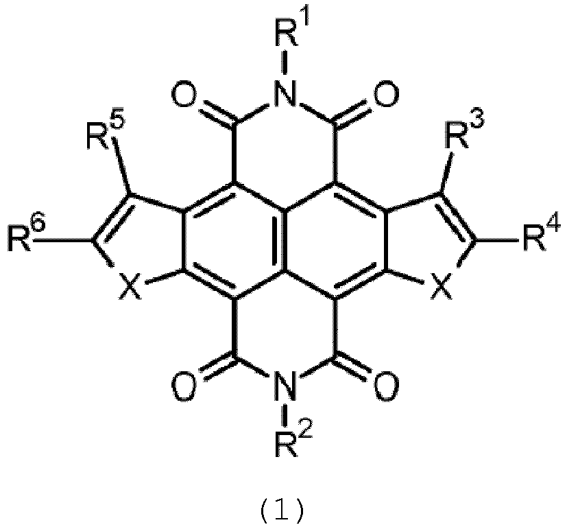
- naphthalene diimides It is known to modify the properties of naphthalene diimides by functionalization of the parent naphthalene diimide core at the 2, 3, 6 and 7 positions. However, lateral core expansion of naphthalene diimides has only been demonstrated recently.
- C 1-10 -alkyl, and C 1-20 -alkyl can be branched or unbranched.
- Examples of C 1-10 -alkyl are methyl, ethyl, n -propyl, isopropyl, n -butyl, sec -butyl, isobutyl, tert -butyl , n -pentyl, neopentyl, isopentyl, n -(1-ethyl)propyl, n -hexyl, n -heptyl, n -octyl, n -(2-ethyl)hexyl, n -nonyl and n -decyl.
- C 1-20 -alkyl examples are C 1-10 -alkyl and n -undecyl, n -dodecyl, n -tridecyl, n -tetradecyl, n -pentadecyl, n -hexadecyl, n -heptadecyl, n -octadecyl, n -nonadecyl and n -icosyl (C 20 ).
- C 6-14 -aryl examples are phenyl and naphthyl.
- halogen examples include F, Cl, Br and I.
- Particular preferred compounds of formulae (1) are the compounds of formulae and
- Particular preferred compounds of formulae (2) are the compounds of formulae and
- the first step of the process or the preparation of a compound of formula (1) is usually performed in a suitable organic solvent such as chloroform.
- the first step of the process is usually performed at an elevated temperature, for example at a temperature of 40 to 100°C, preferably at a temperature of 50 to 80 °C.
- the metal catalyst A of the second step of the process for the preparation of a compound of formula (1) is usually a transition metal catalyst. Preferably, it is a Pd-catalyst such as Pd(OAc) 2 .
- the metal catalyst of the second step of the process is usually used in the presence of a base and a suitable solvent.
- the solvent can be a suitable organic solvent such as DMF.
- the base can be suitable base such as K 2 CO 3 .
- the second step of the process is usually performed at an elevated temperature, for example at a temperature of 50 to 200 °C, preferably at a temperature of 80 to 120 °C.
- the metal catalyst B of the second step of the process for the preparation of a compound of formula (2) is usually a transition metal catalyst. Preferably, it is a Pd-catalyst such as Pd(OAc) 2 .
- the metal catalyst of the second step of the process is usually used in the presence of a base and a suitable solvent.
- the solvent can be a suitable organic solvent such as DMF.
- the base can be suitable base such as K 2 CO 3 .
- the second step of the process is usually performed at an elevated temperature, for example at a temperature of 50 to 200°C, preferably at a temperature of 100 to 160 °C.
- Also part of the invention is an electronic device comprising the compounds of the present invention as semiconducting material.
- the electronic device can be any electronic device, for example an organic photovoltaic (OPV) cell, an organic field-effect transistor (OFET) or an organic light emitting diode (OLED).
- OCV organic photovoltaic
- OFET organic field-effect transistor
- OLED organic light emitting diode
- the electronic device is an organic field-effect transistor.
- an organic field effect transistor comprises a dielectric layer, a semiconducting layer and a substrate.
- an organic field effect transistor usually comprises a gate electrode and source/drain electrodes.
- An organic field effect transistor can have various designs, for example bottom-gate design or top-gate design.
- the substrate can be any suitable substrate such as undoped or highly doped silicon, for example in form of a silicon waver, or glass, or a plastic substrate such as polyethersulfone, polycarbonate, polysulfone, polyethylene terephthalate (PET) and polyethylene naphthalate (PEN).
- a suitable substrate such as undoped or highly doped silicon, for example in form of a silicon waver, or glass
- a plastic substrate such as polyethersulfone, polycarbonate, polysulfone, polyethylene terephthalate (PET) and polyethylene naphthalate (PEN).
- the dielectric layer comprises a dielectric material.
- the dielectric material can be any suitable material such as aluminium oxide, aluminium oxide in combination with a self-assembled monolayer (SAM) of a phosphonic acid such as C 14 H 29 PO(OH) 2 [TDPA] or C 7 F 15 C 11 H 22 PO(OH) 2 [FODPA]), silicon dioxide, or an organic polymer such as polystyrene (PS), poly(methylmethacrylate) (PMMA), poly(4-vinylphenol) (PVP), poly(vinyl alcohol) (PVA), benzocyclobutene (BCB) or polyimide (PI), or a combination of these materials
- the dielectric layer can have a thickness of 5 to 2000 nm, preferably of 5 to 500 nm, more preferably of 5 to 100 nm.
- the semiconducting layer comprises one or more of the compounds of the present invention.
- the semiconducting layer can have a thickness of 5 to 500 nm, preferably of 10 to 100 nm, more preferably of 20 to 50 nm.
- the source/drain electrodes can be made from any suitable source/drain material, for example silver (Ag), gold (Au) or tantalum (Ta).
- the source/drain electrodes can have a thickness of 1 to 100 nm, preferably from 5 to 50 nm.
- the gate electrode can be made from any suitable gate material such as highly doped silicon, aluminium (Al), tungsten (W), indium tin oxide, silver (Ag), gold (Au) or tantalum (Ta), or from a combination of these materials.
- the gate electrode can have a thickness of 1 to 200 nm, preferably from 5 to 100 nm.
- the field effect transistor can be prepared by methods known in the art.
- a bottom-gate organic field effect transistor can be prepared as follows: Aluminium can be deposited on highly doped silicon wafers by thermal evaporation, followed by oxidation of the aluminium layer to aluminium oxide and treatment of the aluminium oxide surface with a phosphonic acid in order to form a self-assembled monolayer (SAM-layer) of the phosphonic acid on the aluminium oxide surface.
- the semiconducting material can be deposited on the SAM-layer by thermal sublimation.
- the source and drain electrodes can be formed by evaporating gold through a shadow mask.
- the back side of the highly doped silicon wafers can be coated with silver ink to serve as the gate electrode.
- a bottom-gate organic field effect transistor can be prepared as follows: Aluminiumoxide can be deposited on highly doped silicon wafers with a thermally grown silicon dioxide layer by atomic layer deposition, followed by treatment of the aluminium oxide surface with a phosphonic acid in order to form a self-assembled monolayer (SAM-layer) of the phosphonic acid on the aluminium oxide surface.
- SAM-layer self-assembled monolayer
- the semiconducting material can be deposited on the SAM-layer by thermal sublimation.
- the source and drain electrodes can be formed by evaporating gold through a shadow mask.
- the back side of the highly doped silicon wafers can coated be with silver ink to serve as the gate electrode.
- Also part of the invention is the use of the compounds of the present invention as semiconducting materials.
- the compounds of the present invention show a high stability, in particular towards oxidation, under ambient conditions.
- Organic devices, in particular organic field effect transistors, comprising compounds of the present invention as semiconducting material show high charge carrier mobilities and high on/off ratios.
- Compound 4a is prepared as described in example 9 of WO 2007/074137 .
- Compound 4b is prepared as described in X. Gao et al., Org. Lett. 2007, 9, 3917 - 3920 .
- 3-Bis(trifluoromethyl)aniline (0.20 mL, 1.2 mmol) is added to a solution of compound 4b (72.3 mg, 0.0898 mmol) in toluene (5 mL). After heating the solution at 70 °C for 4 days 0.1 mL 0.6 mmol) 3-bis(trifluoromethyl)aniline is added. The solution is heated at 70 °C for 2 days more. The solvent is removed under reduced pressure, and the residue is purified by column chromatography (dichloromethane/pentane 1 : 4). A red solid is obtained (80.6 mg, 81 %).
- the compound 5b is prepared in analogy to 5a.
- Highly doped p-type silicon (100) wafers (0.01-0.02 ⁇ cm) were used as substrates A.
- Highly doped p-type silicon (100) wafers (0.005-0.02 ⁇ cm) with a 100 nm thick thermally grown SiO 2 layer (capacitance 34 nF/cm 2 ) were used as substrates B.
- a 30 nm thick layer of aluminum is deposited by thermal evaporation in a Leybold UNIVEX 300 vacuum evaporator from a tungsten wire, at a pressure of 2 ⁇ 10 -6 mbar and with an evaporation rate of 1 nm/s.
- the surface of the aluminum layer is oxidized by a brief exposure to an oxygen plasma in an Oxford reactive ion etcher (RIE, oxygen flow rate: 30 sccm, pressure: 10 mTorr (0.013 mBar), plasma power: 200 W, plasma duration 30 sec) and the substrate is then immersed into a 2-propanol solution of a phosphonic acid (1 mMol solution of C 14 H 29 PO(OH) 2 [TDPA] or 1 mMol solution of C 7 F 15 C 11 H 22 PO(OH) 2 [FODPA]) and left in the solution for 1 hour, which results in the formation of a self-assembled monolayer (SAM) of phosphonic acid molecules on the aluminum oxide surface.
- RIE Oxford reactive ion etcher
- the substrate is taken out of the solution and rinsed with pure 2-propanol, dried in a stream of nitrogen and left for 10 min on a hotplate at a temperature of 100 °C.
- the total capacitance of the AlO x /SAM gate dielectric on substrate A is 810 nF/cm 2 in case of C 14 H 29 PO(OH) 2 and 710 nF/cm 2 in case of C 7 F 15 C 11 H 22 PO(OH) 2 .
- an about 8 nm thick layer of Al 2 O 3 is deposited by atomic layer deposition in a Cambridge NanoTech Savannah (80 cycles at a substrate temperature of 250 °C).
- the surface of the aluminum oxide layer is activated by a brief exposure to an oxygen plasma in an Oxford reactive ion etcher (RIE, oxygen flow rate: 30 sccm, pressure: 10 mTorr (0.013 mBar), plasma power: 200 W, plasma duration 30 sec) and the substrate is then immersed into a 2-propanol solution of a phosphonic acid (1 mMol solution of C 14 H 29 PO(OH) 2 [TDPA] or 1 mMol solution of C 7 F 15 C 11 H 22 PO(OH) 2 [FODPA]) and left in the solution for 1 hour, which results in the formation of a self-assembled monolayer (SAM) of phosphonic acid molecules on the aluminum oxide surface.
- RIE Oxford reactive ion etcher
- the substrate is taken out of the solution and rinsed with pure 2-propanol, dried in a stream of nitrogen and left for 10 min on a hotplate at a temperature of 100 °C.
- the total capacitance of the SiO 2 /AlO x /SAM gate dielectric on substrate B is 32 nF/cm 2 (independent on the choice of the phosphonic acid).
- the contact angle of water on the TDPA-treated substrates is 108°, and on the FODPA-treated substrates 118°.
- a 30 nm thick film of compounds of the present invention as organic semiconductor is deposited by thermal sublimation in a Leybold UNIVEX 300 vacuum evaporator from a molybdenum boat, at a pressure of 2 ⁇ 10 -6 mbar and with an evaporation rate of 0.3 nm/s.
- the transistors have a channel length (L) ranging from 10 to 100 ⁇ m and a channel width (W) ranging from 50 to 1000 ⁇ m.
- the wafer (which also serves as the gate electrode of the transistors) is scratched on the back side and coated with silver ink.
- the electrical characteristics of the transistors are measured on a Micromanipulator 6200 probe station using an Agilent 4156C semiconductor parameter analyzer. All measurements are performed in air at room temperature.
- the probe needles are brought into contact with the source and drain contacts of the transistors by putting them down carefully on top of the gold contacts.
- the gate electrode is contacted through the metal substrate holder onto which the wafer is placed during the measurements.
- the drain-source voltage (V DS ) is held to 3 V (in case of substrate A ) or 40 V (in case of substrate B ).
- the gate-source voltage V GS is swept at medium speed from 0 to 3 V in steps of 0.03 V (substrate A ) or from 0 to 40 V in steps of 0.4 V (substrate B ) and back.
- the charge-carrier mobility is extracted in the saturation regime from the slope of (I D ) 1/2 versus V GS .
- the drain-source voltage (V DS ) is swept at medium speed from 0 to 3 V in steps of 0.03 V (substrate A ) and from 0 to 40 V in steps of 0.4 V (substrate B ), while the gate-source voltage V GS is held at up to 8 different voltages (e.g. 0, 0.5, 1, 1.5, 2, 2.5, 3 V in case of substrate A or 0, 10, 20, 30, 40 V in case of substrate B ).
Landscapes
- Chemical & Material Sciences (AREA)
- Organic Chemistry (AREA)
- Engineering & Computer Science (AREA)
- Materials Engineering (AREA)
- Physics & Mathematics (AREA)
- Spectroscopy & Molecular Physics (AREA)
- Power Engineering (AREA)
- Microelectronics & Electronic Packaging (AREA)
- Heterocyclic Carbon Compounds Containing A Hetero Ring Having Oxygen Or Sulfur (AREA)
- Nitrogen Condensed Heterocyclic Rings (AREA)
- Thin Film Transistor (AREA)
- Organic Low-Molecular-Weight Compounds And Preparation Thereof (AREA)
Claims (6)
- Verbindungen der Formeln
 X für O oder NR13 steht,
wobei R13 für H steht,R1, R2, R7 und R8 unabhängig voneinander für C1-20-Alkyl oder C6-14-Aryl stehen undR3 und R4,R5 und R6,R9 und R10 undR11 und R12zusammen mit den C-Atomen, an die sie gebunden sind, ein C5-14-gliedriges Ringsystem, das aus der Gruppe bestehend aus
wobei
C6-14-Aryl und das C5-14-gliedrige Ringsystem durch einen oder mehrere Substituenten aus der Gruppe bestehend aus C1-10-Alkyl, das durch ein oder mehrere Halogene substituiert sein kann, und Halogen ausgewählt ist, substituiert sein können. - Elektronische Vorrichtung, umfassend die Verbindungen nach Anspruch 1.
- Elektronische Vorrichtung nach Anspruch 2, wobei es sich bei der elektronischen Vorrichtung um einen organischen Feldeffekttransistor handelt.
- Verwendung der Verbindungen nach Anspruch 1 als halbleitende Materialien.
- Verfahren zur Herstellung der Verbindung der Formel
 X für O oder NR13 steht,
wobei R13 für H steht,R1 und R2 unabhängig voneinander für C1-20-Alkyl oder C6-14-Aryl stehen undR3 und R4 undR5 und R6zusammen mit den C-Atomen, an die sie gebunden sind, ein C5-14-gliedriges Ringsystem, das aus der Gruppe bestehend aus
wobei
C6-14-Aryl und das C5-14-gliedrige Ringsystem durch ein oder mehrere C1-10-Alkyl, das durch ein oder mehrere Halogene substituiert sein kann, oder Halogen, substituiert sein können,
wobei das Verfahren folgende Schritte umfasst:(i) Umsetzen einer Verbindung der Formel
mit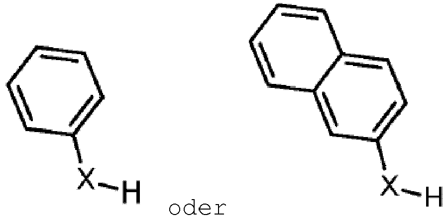
zum Erhalt einer Verbindung der Formel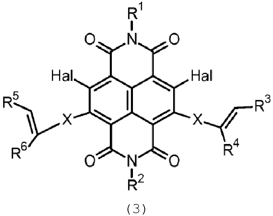
und(ii) Umsetzen der im ersten Schritt erhaltenen Verbindung der Formel (3) mit einem Metallkatalysator A zum Erhalt der Verbindung der Formel (1). - Verfahren zur Herstellung einer Verbindung der Formel (2)
 R7 und R8 unabhängig voneinander für C1-20-Alkyl oder C6-14-Aryl stehen undR9 und R10 undR11 und R12zusammen mit den C-Atomen, an die sie gebunden sind, ein C5-14-gliedriges Ringsystem, das aus der Gruppe bestehend aus
wobei
C6-14-Aryl und das C5-14-gliedrige Ringsystem durch ein oder mehrere C1-10-Alkyl substituiert sein können,
wobei das Verfahren den Schritt des Umsetzens einer Verbindung der Formel

zum Erhalt der Verbindung der Formel (2) umfasst.
Priority Applications (1)
| Application Number | Priority Date | Filing Date | Title |
|---|---|---|---|
| EP14788948.9A EP2989109B1 (de) | 2013-04-25 | 2014-04-22 | Herstellung von pi-erweiterten naphthalin-diimiden und deren verwendung als halbleiter |
Applications Claiming Priority (3)
| Application Number | Priority Date | Filing Date | Title |
|---|---|---|---|
| EP13165368 | 2013-04-25 | ||
| EP14788948.9A EP2989109B1 (de) | 2013-04-25 | 2014-04-22 | Herstellung von pi-erweiterten naphthalin-diimiden und deren verwendung als halbleiter |
| PCT/IB2014/060902 WO2014174435A2 (en) | 2013-04-25 | 2014-04-22 | Preparation of pi-extended naphthalene diimides and their use as semiconductor |
Publications (3)
| Publication Number | Publication Date |
|---|---|
| EP2989109A2 EP2989109A2 (de) | 2016-03-02 |
| EP2989109A4 EP2989109A4 (de) | 2017-01-18 |
| EP2989109B1 true EP2989109B1 (de) | 2019-09-11 |
Family
ID=48190232
Family Applications (1)
| Application Number | Title | Priority Date | Filing Date |
|---|---|---|---|
| EP14788948.9A Active EP2989109B1 (de) | 2013-04-25 | 2014-04-22 | Herstellung von pi-erweiterten naphthalin-diimiden und deren verwendung als halbleiter |
Country Status (6)
| Country | Link |
|---|---|
| US (1) | US9444058B2 (de) |
| EP (1) | EP2989109B1 (de) |
| JP (1) | JP6033497B2 (de) |
| KR (1) | KR20150142043A (de) |
| CN (1) | CN105143231B (de) |
| WO (1) | WO2014174435A2 (de) |
Families Citing this family (6)
| Publication number | Priority date | Publication date | Assignee | Title |
|---|---|---|---|---|
| EP3278379A1 (de) * | 2015-03-31 | 2018-02-07 | Sony Corporation | N- und p-aktive materialien für organische fotoelektrische konversionsschichten in organischen fotodioden |
| EP3333917B1 (de) * | 2015-08-04 | 2022-04-06 | FUJIFILM Corporation | Organischer dünnschichttransistor, verfahren zur herstellung eines organischen dünnschichttransistors, material für organische dünnfilmtransistoren, zusammensetzung für organische dünnschichttransistoren, organische halbleiterschicht und verbindung |
| JP2017043590A (ja) * | 2015-08-28 | 2017-03-02 | 国立研究開発法人理化学研究所 | 新規な化合物、新規なポリマーおよびその利用 |
| WO2019170481A1 (en) | 2018-03-07 | 2019-09-12 | Basf Se | Patterning method for preparing top-gate, bottom-contact organic field effect transistors |
| WO2019170719A1 (en) | 2018-03-08 | 2019-09-12 | Basf Se | Organic field effect transistor comprising semiconducting single-walled carbon nanotubes and organic semiconducting material |
| CN112074548B (zh) | 2018-06-26 | 2023-07-25 | Clap有限公司 | 作为电介质的乙烯醚类聚合物 |
Family Cites Families (8)
| Publication number | Priority date | Publication date | Assignee | Title |
|---|---|---|---|---|
| DE102005061997A1 (de) | 2005-12-23 | 2007-07-05 | Basf Ag | Naphthalintetracarbonsäurederivate und deren Verwendung |
| US8664339B2 (en) * | 2008-11-07 | 2014-03-04 | Polyera Corporation | Organic semiconducting polymers |
| CN101885732B (zh) * | 2010-06-23 | 2012-06-27 | 中国科学院上海有机化学研究所 | 硫杂环稠合的萘四羧酸二酰亚胺衍生物、及制法和应用 |
| CN101693719B (zh) | 2009-10-23 | 2012-07-04 | 中国科学院上海有机化学研究所 | 以萘四羧酸二酰亚胺为核的硫杂共轭化合物、制法和应用 |
| EP2492271B1 (de) * | 2009-10-23 | 2018-05-09 | Shanghai Institute Of Organic Chemistry, Chinese Academy Of Sciences | Schwefelhaltige heterozyklisch fusionierte naphthalen-tetracarboxylsäure-diimid-derivate sowie herstellungsverfahren dafür und verwendung davon |
| JP6132470B2 (ja) * | 2011-04-12 | 2017-05-24 | ユー・ディー・シー アイルランド リミテッド | 有機電界発光素子、該素子に用いる化合物および有機電界発光素子用材料、並びに該素子を用いた発光装置、表示装置及び照明装置 |
| CN103874742B (zh) * | 2011-08-12 | 2016-08-17 | 巴斯夫欧洲公司 | 咔唑并咔唑-二(二碳酰亚胺)和它们作为半导体的用途 |
| JP6012148B2 (ja) * | 2011-08-22 | 2016-10-25 | ユー・ディー・シー アイルランド リミテッド | 有機電界発光素子、化合物、並びに該素子を用いた発光装置、表示装置及び照明装置 |
-
2014
- 2014-04-22 KR KR1020157032400A patent/KR20150142043A/ko active Search and Examination
- 2014-04-22 CN CN201480023312.2A patent/CN105143231B/zh active Active
- 2014-04-22 EP EP14788948.9A patent/EP2989109B1/de active Active
- 2014-04-22 JP JP2016509578A patent/JP6033497B2/ja active Active
- 2014-04-22 US US14/786,024 patent/US9444058B2/en active Active
- 2014-04-22 WO PCT/IB2014/060902 patent/WO2014174435A2/en active Application Filing
Non-Patent Citations (1)
| Title |
|---|
| None * |
Also Published As
| Publication number | Publication date |
|---|---|
| EP2989109A4 (de) | 2017-01-18 |
| CN105143231B (zh) | 2019-01-22 |
| JP2016520042A (ja) | 2016-07-11 |
| US9444058B2 (en) | 2016-09-13 |
| JP6033497B2 (ja) | 2016-11-30 |
| EP2989109A2 (de) | 2016-03-02 |
| WO2014174435A3 (en) | 2015-03-12 |
| WO2014174435A2 (en) | 2014-10-30 |
| CN105143231A (zh) | 2015-12-09 |
| KR20150142043A (ko) | 2015-12-21 |
| US20160104846A1 (en) | 2016-04-14 |
Similar Documents
| Publication | Publication Date | Title |
|---|---|---|
| EP2989109B1 (de) | Herstellung von pi-erweiterten naphthalin-diimiden und deren verwendung als halbleiter | |
| KR101410150B1 (ko) | 전계 효과 트랜지스터 | |
| TWI410427B (zh) | 甲矽烷基乙炔基化雜環並化合物及利用其所製之電子裝置 | |
| US7385221B1 (en) | Silylethynylated heteroacenes and electronic devices made therewith | |
| EP2086974B1 (de) | Halbleitermaterialien auf diimidbasis und verfahren zu deren herstellung und anwendung | |
| Kozycz et al. | Enhanced electron mobility in crystalline thionated naphthalene diimides | |
| US20180175305A1 (en) | Azaazene analogues and their use as semiconductor | |
| Chen et al. | Asymmetric fused thiophenes for field-effect transistors: crystal structure–film microstructure–transistor performance correlations | |
| TW201006840A (en) | Perylene semiconductors and methods of preparation and use thereof | |
| JP2008513544A (ja) | カルボニル官能化チオフェン化合物および関連する装置構造 | |
| Chen et al. | Angular-shaped naphthalene tetracarboxylic diimides for n-channel organic transistor semiconductors | |
| WO2012118174A1 (ja) | 有機電界効果トランジスタ及び有機半導体材料 | |
| Chang et al. | 6, 13-Dicyano pentacene-2, 3: 9, 10-bis (dicarboximide) for solution-processed air-stable n-channel field effect transistors and complementary circuit | |
| Gao et al. | Linear benzene-fused bis (tetrathiafulvalene) compounds for solution processed organic field-effect transistors | |
| EP3110807B1 (de) | Heteroazene für organische elektronik | |
| Ie et al. | Perfluoroalkyl-annelated conjugated systems toward n-type organic semiconductors | |
| Chen et al. | New core-expanded naphthalene diimides with different functional groups for air-stable solution-processed organic n-type semiconductors | |
| Lee et al. | Synthesis and characterization of fluorenone-based donor-acceptor small molecule organic semiconductors for organic field-effect transistors | |
| JP5428113B2 (ja) | 電界効果トランジスタ | |
| Birajdar et al. | Influences of the number of 2-ethylhexylamine chain substituents on electron transport characteristics of core-substituted naphthalene diimide analogues | |
| Li et al. | High-performance electron-transporting hybrid rylenes with low threshold voltage | |
| US8513466B2 (en) | Class of soluble, photooxidatively resistant acene derivatives | |
| Kim et al. | Synthesis and characterization of 2, 7-diethynyl-benzo [b] benzo [4, 5] thieno [2, 3-d] thiophene derivative as organic semiconductors for organic thin-film transistors | |
| TWI542591B (zh) | 四氮雜靴二蒽化合物及其作為n-型半導體之用途 | |
| Yu et al. | Functionalized soluble triethylsilylethynyl anthradithiophenes (TESADTs) for organic electronic devices |
Legal Events
| Date | Code | Title | Description |
|---|---|---|---|
| PUAI | Public reference made under article 153(3) epc to a published international application that has entered the european phase |
Free format text: ORIGINAL CODE: 0009012 |
|
| 17P | Request for examination filed |
Effective date: 20151125 |
|
| AK | Designated contracting states |
Kind code of ref document: A2 Designated state(s): AL AT BE BG CH CY CZ DE DK EE ES FI FR GB GR HR HU IE IS IT LI LT LU LV MC MK MT NL NO PL PT RO RS SE SI SK SM TR |
|
| AX | Request for extension of the european patent |
Extension state: BA ME |
|
| DAX | Request for extension of the european patent (deleted) | ||
| REG | Reference to a national code |
Ref country code: DE Ref legal event code: R079 Ref document number: 602014053512 Country of ref document: DE Free format text: PREVIOUS MAIN CLASS: C07D0495220000 Ipc: C07D0471220000 |
|
| A4 | Supplementary search report drawn up and despatched |
Effective date: 20161219 |
|
| RIC1 | Information provided on ipc code assigned before grant |
Ipc: C09B 23/04 20060101ALI20161213BHEP Ipc: C07D 471/22 20060101AFI20161213BHEP Ipc: H01G 9/20 20060101ALI20161213BHEP Ipc: C07D 491/22 20060101ALI20161213BHEP Ipc: H01L 51/00 20060101ALI20161213BHEP Ipc: C09B 5/62 20060101ALI20161213BHEP |
|
| STAA | Information on the status of an ep patent application or granted ep patent |
Free format text: STATUS: EXAMINATION IS IN PROGRESS |
|
| 17Q | First examination report despatched |
Effective date: 20180115 |
|
| GRAP | Despatch of communication of intention to grant a patent |
Free format text: ORIGINAL CODE: EPIDOSNIGR1 |
|
| STAA | Information on the status of an ep patent application or granted ep patent |
Free format text: STATUS: GRANT OF PATENT IS INTENDED |
|
| INTG | Intention to grant announced |
Effective date: 20190404 |
|
| RIN1 | Information on inventor provided before grant (corrected) |
Inventor name: SURARU, SABIN-LUCIAN Inventor name: GESSNER, THOMAS Inventor name: WUERTHNER, FRANK |
|
| GRAS | Grant fee paid |
Free format text: ORIGINAL CODE: EPIDOSNIGR3 |
|
| GRAA | (expected) grant |
Free format text: ORIGINAL CODE: 0009210 |
|
| STAA | Information on the status of an ep patent application or granted ep patent |
Free format text: STATUS: THE PATENT HAS BEEN GRANTED |
|
| AK | Designated contracting states |
Kind code of ref document: B1 Designated state(s): AL AT BE BG CH CY CZ DE DK EE ES FI FR GB GR HR HU IE IS IT LI LT LU LV MC MK MT NL NO PL PT RO RS SE SI SK SM TR |
|
| REG | Reference to a national code |
Ref country code: GB Ref legal event code: FG4D |
|
| REG | Reference to a national code |
Ref country code: CH Ref legal event code: EP |
|
| REG | Reference to a national code |
Ref country code: AT Ref legal event code: REF Ref document number: 1178317 Country of ref document: AT Kind code of ref document: T Effective date: 20190915 |
|
| REG | Reference to a national code |
Ref country code: DE Ref legal event code: R096 Ref document number: 602014053512 Country of ref document: DE Ref country code: IE Ref legal event code: FG4D |
|
| REG | Reference to a national code |
Ref country code: NL Ref legal event code: MP Effective date: 20190911 |
|
| REG | Reference to a national code |
Ref country code: LT Ref legal event code: MG4D |
|
| PG25 | Lapsed in a contracting state [announced via postgrant information from national office to epo] |
Ref country code: FI Free format text: LAPSE BECAUSE OF FAILURE TO SUBMIT A TRANSLATION OF THE DESCRIPTION OR TO PAY THE FEE WITHIN THE PRESCRIBED TIME-LIMIT Effective date: 20190911 Ref country code: NO Free format text: LAPSE BECAUSE OF FAILURE TO SUBMIT A TRANSLATION OF THE DESCRIPTION OR TO PAY THE FEE WITHIN THE PRESCRIBED TIME-LIMIT Effective date: 20191211 Ref country code: SE Free format text: LAPSE BECAUSE OF FAILURE TO SUBMIT A TRANSLATION OF THE DESCRIPTION OR TO PAY THE FEE WITHIN THE PRESCRIBED TIME-LIMIT Effective date: 20190911 Ref country code: LT Free format text: LAPSE BECAUSE OF FAILURE TO SUBMIT A TRANSLATION OF THE DESCRIPTION OR TO PAY THE FEE WITHIN THE PRESCRIBED TIME-LIMIT Effective date: 20190911 Ref country code: HR Free format text: LAPSE BECAUSE OF FAILURE TO SUBMIT A TRANSLATION OF THE DESCRIPTION OR TO PAY THE FEE WITHIN THE PRESCRIBED TIME-LIMIT Effective date: 20190911 Ref country code: BG Free format text: LAPSE BECAUSE OF FAILURE TO SUBMIT A TRANSLATION OF THE DESCRIPTION OR TO PAY THE FEE WITHIN THE PRESCRIBED TIME-LIMIT Effective date: 20191211 |
|
| PG25 | Lapsed in a contracting state [announced via postgrant information from national office to epo] |
Ref country code: AL Free format text: LAPSE BECAUSE OF FAILURE TO SUBMIT A TRANSLATION OF THE DESCRIPTION OR TO PAY THE FEE WITHIN THE PRESCRIBED TIME-LIMIT Effective date: 20190911 Ref country code: LV Free format text: LAPSE BECAUSE OF FAILURE TO SUBMIT A TRANSLATION OF THE DESCRIPTION OR TO PAY THE FEE WITHIN THE PRESCRIBED TIME-LIMIT Effective date: 20190911 Ref country code: RS Free format text: LAPSE BECAUSE OF FAILURE TO SUBMIT A TRANSLATION OF THE DESCRIPTION OR TO PAY THE FEE WITHIN THE PRESCRIBED TIME-LIMIT Effective date: 20190911 Ref country code: GR Free format text: LAPSE BECAUSE OF FAILURE TO SUBMIT A TRANSLATION OF THE DESCRIPTION OR TO PAY THE FEE WITHIN THE PRESCRIBED TIME-LIMIT Effective date: 20191212 Ref country code: ES Free format text: LAPSE BECAUSE OF FAILURE TO SUBMIT A TRANSLATION OF THE DESCRIPTION OR TO PAY THE FEE WITHIN THE PRESCRIBED TIME-LIMIT Effective date: 20190911 |
|
| REG | Reference to a national code |
Ref country code: AT Ref legal event code: MK05 Ref document number: 1178317 Country of ref document: AT Kind code of ref document: T Effective date: 20190911 |
|
| PG25 | Lapsed in a contracting state [announced via postgrant information from national office to epo] |
Ref country code: RO Free format text: LAPSE BECAUSE OF FAILURE TO SUBMIT A TRANSLATION OF THE DESCRIPTION OR TO PAY THE FEE WITHIN THE PRESCRIBED TIME-LIMIT Effective date: 20190911 Ref country code: PT Free format text: LAPSE BECAUSE OF FAILURE TO SUBMIT A TRANSLATION OF THE DESCRIPTION OR TO PAY THE FEE WITHIN THE PRESCRIBED TIME-LIMIT Effective date: 20200113 Ref country code: PL Free format text: LAPSE BECAUSE OF FAILURE TO SUBMIT A TRANSLATION OF THE DESCRIPTION OR TO PAY THE FEE WITHIN THE PRESCRIBED TIME-LIMIT Effective date: 20190911 Ref country code: AT Free format text: LAPSE BECAUSE OF FAILURE TO SUBMIT A TRANSLATION OF THE DESCRIPTION OR TO PAY THE FEE WITHIN THE PRESCRIBED TIME-LIMIT Effective date: 20190911 Ref country code: NL Free format text: LAPSE BECAUSE OF FAILURE TO SUBMIT A TRANSLATION OF THE DESCRIPTION OR TO PAY THE FEE WITHIN THE PRESCRIBED TIME-LIMIT Effective date: 20190911 Ref country code: EE Free format text: LAPSE BECAUSE OF FAILURE TO SUBMIT A TRANSLATION OF THE DESCRIPTION OR TO PAY THE FEE WITHIN THE PRESCRIBED TIME-LIMIT Effective date: 20190911 |
|
| PG25 | Lapsed in a contracting state [announced via postgrant information from national office to epo] |
Ref country code: CZ Free format text: LAPSE BECAUSE OF FAILURE TO SUBMIT A TRANSLATION OF THE DESCRIPTION OR TO PAY THE FEE WITHIN THE PRESCRIBED TIME-LIMIT Effective date: 20190911 Ref country code: SM Free format text: LAPSE BECAUSE OF FAILURE TO SUBMIT A TRANSLATION OF THE DESCRIPTION OR TO PAY THE FEE WITHIN THE PRESCRIBED TIME-LIMIT Effective date: 20190911 Ref country code: SK Free format text: LAPSE BECAUSE OF FAILURE TO SUBMIT A TRANSLATION OF THE DESCRIPTION OR TO PAY THE FEE WITHIN THE PRESCRIBED TIME-LIMIT Effective date: 20190911 Ref country code: IS Free format text: LAPSE BECAUSE OF FAILURE TO SUBMIT A TRANSLATION OF THE DESCRIPTION OR TO PAY THE FEE WITHIN THE PRESCRIBED TIME-LIMIT Effective date: 20200224 |
|
| REG | Reference to a national code |
Ref country code: DE Ref legal event code: R097 Ref document number: 602014053512 Country of ref document: DE |
|
| PLBE | No opposition filed within time limit |
Free format text: ORIGINAL CODE: 0009261 |
|
| STAA | Information on the status of an ep patent application or granted ep patent |
Free format text: STATUS: NO OPPOSITION FILED WITHIN TIME LIMIT |
|
| PG2D | Information on lapse in contracting state deleted |
Ref country code: IS |
|
| PG25 | Lapsed in a contracting state [announced via postgrant information from national office to epo] |
Ref country code: DK Free format text: LAPSE BECAUSE OF FAILURE TO SUBMIT A TRANSLATION OF THE DESCRIPTION OR TO PAY THE FEE WITHIN THE PRESCRIBED TIME-LIMIT Effective date: 20190911 Ref country code: IS Free format text: LAPSE BECAUSE OF FAILURE TO SUBMIT A TRANSLATION OF THE DESCRIPTION OR TO PAY THE FEE WITHIN THE PRESCRIBED TIME-LIMIT Effective date: 20200112 |
|
| 26N | No opposition filed |
Effective date: 20200615 |
|
| PG25 | Lapsed in a contracting state [announced via postgrant information from national office to epo] |
Ref country code: SI Free format text: LAPSE BECAUSE OF FAILURE TO SUBMIT A TRANSLATION OF THE DESCRIPTION OR TO PAY THE FEE WITHIN THE PRESCRIBED TIME-LIMIT Effective date: 20190911 |
|
| PG25 | Lapsed in a contracting state [announced via postgrant information from national office to epo] |
Ref country code: MC Free format text: LAPSE BECAUSE OF FAILURE TO SUBMIT A TRANSLATION OF THE DESCRIPTION OR TO PAY THE FEE WITHIN THE PRESCRIBED TIME-LIMIT Effective date: 20190911 |
|
| REG | Reference to a national code |
Ref country code: CH Ref legal event code: PL |
|
| PG25 | Lapsed in a contracting state [announced via postgrant information from national office to epo] |
Ref country code: LU Free format text: LAPSE BECAUSE OF NON-PAYMENT OF DUE FEES Effective date: 20200422 Ref country code: LI Free format text: LAPSE BECAUSE OF NON-PAYMENT OF DUE FEES Effective date: 20200430 Ref country code: CH Free format text: LAPSE BECAUSE OF NON-PAYMENT OF DUE FEES Effective date: 20200430 |
|
| REG | Reference to a national code |
Ref country code: BE Ref legal event code: MM Effective date: 20200430 |
|
| PG25 | Lapsed in a contracting state [announced via postgrant information from national office to epo] |
Ref country code: BE Free format text: LAPSE BECAUSE OF NON-PAYMENT OF DUE FEES Effective date: 20200430 |
|
| PG25 | Lapsed in a contracting state [announced via postgrant information from national office to epo] |
Ref country code: IE Free format text: LAPSE BECAUSE OF NON-PAYMENT OF DUE FEES Effective date: 20200422 |
|
| REG | Reference to a national code |
Ref country code: DE Ref legal event code: R082 Ref document number: 602014053512 Country of ref document: DE Representative=s name: REITSTOETTER - KINZEBACH, DE Ref country code: DE Ref legal event code: R082 Ref document number: 602014053512 Country of ref document: DE |
|
| REG | Reference to a national code |
Ref country code: GB Ref legal event code: 732E Free format text: REGISTERED BETWEEN 20220324 AND 20220330 |
|
| PG25 | Lapsed in a contracting state [announced via postgrant information from national office to epo] |
Ref country code: TR Free format text: LAPSE BECAUSE OF FAILURE TO SUBMIT A TRANSLATION OF THE DESCRIPTION OR TO PAY THE FEE WITHIN THE PRESCRIBED TIME-LIMIT Effective date: 20190911 Ref country code: MT Free format text: LAPSE BECAUSE OF FAILURE TO SUBMIT A TRANSLATION OF THE DESCRIPTION OR TO PAY THE FEE WITHIN THE PRESCRIBED TIME-LIMIT Effective date: 20190911 Ref country code: CY Free format text: LAPSE BECAUSE OF FAILURE TO SUBMIT A TRANSLATION OF THE DESCRIPTION OR TO PAY THE FEE WITHIN THE PRESCRIBED TIME-LIMIT Effective date: 20190911 |
|
| PG25 | Lapsed in a contracting state [announced via postgrant information from national office to epo] |
Ref country code: MK Free format text: LAPSE BECAUSE OF FAILURE TO SUBMIT A TRANSLATION OF THE DESCRIPTION OR TO PAY THE FEE WITHIN THE PRESCRIBED TIME-LIMIT Effective date: 20190911 |
|
| REG | Reference to a national code |
Ref country code: DE Ref legal event code: R081 Ref document number: 602014053512 Country of ref document: DE Owner name: CLAP CO., LTD., KR Free format text: FORMER OWNER: BASF SE, 67063 LUDWIGSHAFEN, DE Ref country code: DE Ref legal event code: R082 Ref document number: 602014053512 Country of ref document: DE Representative=s name: REITSTOETTER - KINZEBACH, DE |
|
| REG | Reference to a national code |
Ref country code: FR Ref legal event code: PLFP Year of fee payment: 10 |
|
| PGFP | Annual fee paid to national office [announced via postgrant information from national office to epo] |
Ref country code: GB Payment date: 20230330 Year of fee payment: 10 |
|
| PGFP | Annual fee paid to national office [announced via postgrant information from national office to epo] |
Ref country code: IT Payment date: 20230412 Year of fee payment: 10 Ref country code: FR Payment date: 20230411 Year of fee payment: 10 Ref country code: DE Payment date: 20230331 Year of fee payment: 10 |