EP2988914B1 - Vorrichtung und verfahren zur herstellung einer struktur aus aushärtbarem material durch abformung - Google Patents
Vorrichtung und verfahren zur herstellung einer struktur aus aushärtbarem material durch abformung Download PDFInfo
- Publication number
- EP2988914B1 EP2988914B1 EP14716794.4A EP14716794A EP2988914B1 EP 2988914 B1 EP2988914 B1 EP 2988914B1 EP 14716794 A EP14716794 A EP 14716794A EP 2988914 B1 EP2988914 B1 EP 2988914B1
- Authority
- EP
- European Patent Office
- Prior art keywords
- curable material
- radiation
- molding
- molding tool
- channel
- Prior art date
- Legal status (The legal status is an assumption and is not a legal conclusion. Google has not performed a legal analysis and makes no representation as to the accuracy of the status listed.)
- Active
Links
Images


Classifications
-
- B—PERFORMING OPERATIONS; TRANSPORTING
- B29—WORKING OF PLASTICS; WORKING OF SUBSTANCES IN A PLASTIC STATE IN GENERAL
- B29C—SHAPING OR JOINING OF PLASTICS; SHAPING OF MATERIAL IN A PLASTIC STATE, NOT OTHERWISE PROVIDED FOR; AFTER-TREATMENT OF THE SHAPED PRODUCTS, e.g. REPAIRING
- B29C35/00—Heating, cooling or curing, e.g. crosslinking or vulcanising; Apparatus therefor
- B29C35/02—Heating or curing, e.g. crosslinking or vulcanizing during moulding, e.g. in a mould
- B29C35/08—Heating or curing, e.g. crosslinking or vulcanizing during moulding, e.g. in a mould by wave energy or particle radiation
- B29C35/0805—Heating or curing, e.g. crosslinking or vulcanizing during moulding, e.g. in a mould by wave energy or particle radiation using electromagnetic radiation
-
- B—PERFORMING OPERATIONS; TRANSPORTING
- B29—WORKING OF PLASTICS; WORKING OF SUBSTANCES IN A PLASTIC STATE IN GENERAL
- B29C—SHAPING OR JOINING OF PLASTICS; SHAPING OF MATERIAL IN A PLASTIC STATE, NOT OTHERWISE PROVIDED FOR; AFTER-TREATMENT OF THE SHAPED PRODUCTS, e.g. REPAIRING
- B29C35/00—Heating, cooling or curing, e.g. crosslinking or vulcanising; Apparatus therefor
- B29C35/02—Heating or curing, e.g. crosslinking or vulcanizing during moulding, e.g. in a mould
- B29C35/0288—Controlling heating or curing of polymers during moulding, e.g. by measuring temperatures or properties of the polymer and regulating the process
-
- B—PERFORMING OPERATIONS; TRANSPORTING
- B29—WORKING OF PLASTICS; WORKING OF SUBSTANCES IN A PLASTIC STATE IN GENERAL
- B29C—SHAPING OR JOINING OF PLASTICS; SHAPING OF MATERIAL IN A PLASTIC STATE, NOT OTHERWISE PROVIDED FOR; AFTER-TREATMENT OF THE SHAPED PRODUCTS, e.g. REPAIRING
- B29C37/00—Component parts, details, accessories or auxiliary operations, not covered by group B29C33/00 or B29C35/00
- B29C37/005—Compensating volume or shape change during moulding, in general
-
- B—PERFORMING OPERATIONS; TRANSPORTING
- B29—WORKING OF PLASTICS; WORKING OF SUBSTANCES IN A PLASTIC STATE IN GENERAL
- B29C—SHAPING OR JOINING OF PLASTICS; SHAPING OF MATERIAL IN A PLASTIC STATE, NOT OTHERWISE PROVIDED FOR; AFTER-TREATMENT OF THE SHAPED PRODUCTS, e.g. REPAIRING
- B29C43/00—Compression moulding, i.e. applying external pressure to flow the moulding material; Apparatus therefor
- B29C43/003—Compression moulding, i.e. applying external pressure to flow the moulding material; Apparatus therefor characterised by the choice of material
-
- B—PERFORMING OPERATIONS; TRANSPORTING
- B29—WORKING OF PLASTICS; WORKING OF SUBSTANCES IN A PLASTIC STATE IN GENERAL
- B29C—SHAPING OR JOINING OF PLASTICS; SHAPING OF MATERIAL IN A PLASTIC STATE, NOT OTHERWISE PROVIDED FOR; AFTER-TREATMENT OF THE SHAPED PRODUCTS, e.g. REPAIRING
- B29C43/00—Compression moulding, i.e. applying external pressure to flow the moulding material; Apparatus therefor
- B29C43/32—Component parts, details or accessories; Auxiliary operations
-
- B—PERFORMING OPERATIONS; TRANSPORTING
- B29—WORKING OF PLASTICS; WORKING OF SUBSTANCES IN A PLASTIC STATE IN GENERAL
- B29D—PRODUCING PARTICULAR ARTICLES FROM PLASTICS OR FROM SUBSTANCES IN A PLASTIC STATE
- B29D11/00—Producing optical elements, e.g. lenses or prisms
- B29D11/00009—Production of simple or compound lenses
- B29D11/00432—Auxiliary operations, e.g. machines for filling the moulds
- B29D11/00442—Curing the lens material
-
- G—PHYSICS
- G03—PHOTOGRAPHY; CINEMATOGRAPHY; ANALOGOUS TECHNIQUES USING WAVES OTHER THAN OPTICAL WAVES; ELECTROGRAPHY; HOLOGRAPHY
- G03F—PHOTOMECHANICAL PRODUCTION OF TEXTURED OR PATTERNED SURFACES, e.g. FOR PRINTING, FOR PROCESSING OF SEMICONDUCTOR DEVICES; MATERIALS THEREFOR; ORIGINALS THEREFOR; APPARATUS SPECIALLY ADAPTED THEREFOR
- G03F7/00—Photomechanical, e.g. photolithographic, production of textured or patterned surfaces, e.g. printing surfaces; Materials therefor, e.g. comprising photoresists; Apparatus specially adapted therefor
- G03F7/0002—Lithographic processes using patterning methods other than those involving the exposure to radiation, e.g. by stamping
-
- B—PERFORMING OPERATIONS; TRANSPORTING
- B29—WORKING OF PLASTICS; WORKING OF SUBSTANCES IN A PLASTIC STATE IN GENERAL
- B29C—SHAPING OR JOINING OF PLASTICS; SHAPING OF MATERIAL IN A PLASTIC STATE, NOT OTHERWISE PROVIDED FOR; AFTER-TREATMENT OF THE SHAPED PRODUCTS, e.g. REPAIRING
- B29C35/00—Heating, cooling or curing, e.g. crosslinking or vulcanising; Apparatus therefor
- B29C35/02—Heating or curing, e.g. crosslinking or vulcanizing during moulding, e.g. in a mould
- B29C35/08—Heating or curing, e.g. crosslinking or vulcanizing during moulding, e.g. in a mould by wave energy or particle radiation
- B29C35/0805—Heating or curing, e.g. crosslinking or vulcanizing during moulding, e.g. in a mould by wave energy or particle radiation using electromagnetic radiation
- B29C2035/0827—Heating or curing, e.g. crosslinking or vulcanizing during moulding, e.g. in a mould by wave energy or particle radiation using electromagnetic radiation using UV radiation
-
- B—PERFORMING OPERATIONS; TRANSPORTING
- B29—WORKING OF PLASTICS; WORKING OF SUBSTANCES IN A PLASTIC STATE IN GENERAL
- B29C—SHAPING OR JOINING OF PLASTICS; SHAPING OF MATERIAL IN A PLASTIC STATE, NOT OTHERWISE PROVIDED FOR; AFTER-TREATMENT OF THE SHAPED PRODUCTS, e.g. REPAIRING
- B29C43/00—Compression moulding, i.e. applying external pressure to flow the moulding material; Apparatus therefor
- B29C43/32—Component parts, details or accessories; Auxiliary operations
- B29C43/58—Measuring, controlling or regulating
- B29C2043/5891—Measuring, controlling or regulating using imaging devices, e.g. cameras
-
- B—PERFORMING OPERATIONS; TRANSPORTING
- B29—WORKING OF PLASTICS; WORKING OF SUBSTANCES IN A PLASTIC STATE IN GENERAL
- B29D—PRODUCING PARTICULAR ARTICLES FROM PLASTICS OR FROM SUBSTANCES IN A PLASTIC STATE
- B29D11/00—Producing optical elements, e.g. lenses or prisms
- B29D11/00009—Production of simple or compound lenses
- B29D11/00038—Production of contact lenses
- B29D11/00125—Auxiliary operations, e.g. removing oxygen from the mould, conveying moulds from a storage to the production line in an inert atmosphere
- B29D11/00134—Curing of the contact lens material
-
- B—PERFORMING OPERATIONS; TRANSPORTING
- B29—WORKING OF PLASTICS; WORKING OF SUBSTANCES IN A PLASTIC STATE IN GENERAL
- B29D—PRODUCING PARTICULAR ARTICLES FROM PLASTICS OR FROM SUBSTANCES IN A PLASTIC STATE
- B29D11/00—Producing optical elements, e.g. lenses or prisms
- B29D11/00009—Production of simple or compound lenses
- B29D11/00365—Production of microlenses
-
- B—PERFORMING OPERATIONS; TRANSPORTING
- B29—WORKING OF PLASTICS; WORKING OF SUBSTANCES IN A PLASTIC STATE IN GENERAL
- B29D—PRODUCING PARTICULAR ARTICLES FROM PLASTICS OR FROM SUBSTANCES IN A PLASTIC STATE
- B29D11/00—Producing optical elements, e.g. lenses or prisms
- B29D11/00009—Production of simple or compound lenses
- B29D11/0048—Moulds for lenses
-
- B—PERFORMING OPERATIONS; TRANSPORTING
- B29—WORKING OF PLASTICS; WORKING OF SUBSTANCES IN A PLASTIC STATE IN GENERAL
- B29K—INDEXING SCHEME ASSOCIATED WITH SUBCLASSES B29B, B29C OR B29D, RELATING TO MOULDING MATERIALS OR TO MATERIALS FOR MOULDS, REINFORCEMENTS, FILLERS OR PREFORMED PARTS, e.g. INSERTS
- B29K2101/00—Use of unspecified macromolecular compounds as moulding material
-
- B—PERFORMING OPERATIONS; TRANSPORTING
- B29—WORKING OF PLASTICS; WORKING OF SUBSTANCES IN A PLASTIC STATE IN GENERAL
- B29K—INDEXING SCHEME ASSOCIATED WITH SUBCLASSES B29B, B29C OR B29D, RELATING TO MOULDING MATERIALS OR TO MATERIALS FOR MOULDS, REINFORCEMENTS, FILLERS OR PREFORMED PARTS, e.g. INSERTS
- B29K2105/00—Condition, form or state of moulded material or of the material to be shaped
- B29K2105/24—Condition, form or state of moulded material or of the material to be shaped crosslinked or vulcanised
-
- G—PHYSICS
- G03—PHOTOGRAPHY; CINEMATOGRAPHY; ANALOGOUS TECHNIQUES USING WAVES OTHER THAN OPTICAL WAVES; ELECTROGRAPHY; HOLOGRAPHY
- G03F—PHOTOMECHANICAL PRODUCTION OF TEXTURED OR PATTERNED SURFACES, e.g. FOR PRINTING, FOR PROCESSING OF SEMICONDUCTOR DEVICES; MATERIALS THEREFOR; ORIGINALS THEREFOR; APPARATUS SPECIALLY ADAPTED THEREFOR
- G03F7/00—Photomechanical, e.g. photolithographic, production of textured or patterned surfaces, e.g. printing surfaces; Materials therefor, e.g. comprising photoresists; Apparatus specially adapted therefor
- G03F7/20—Exposure; Apparatus therefor
- G03F7/2002—Exposure; Apparatus therefor with visible light or UV light, through an original having an opaque pattern on a transparent support, e.g. film printing, projection printing; by reflection of visible or UV light from an original such as a printed image
-
- G—PHYSICS
- G03—PHOTOGRAPHY; CINEMATOGRAPHY; ANALOGOUS TECHNIQUES USING WAVES OTHER THAN OPTICAL WAVES; ELECTROGRAPHY; HOLOGRAPHY
- G03F—PHOTOMECHANICAL PRODUCTION OF TEXTURED OR PATTERNED SURFACES, e.g. FOR PRINTING, FOR PROCESSING OF SEMICONDUCTOR DEVICES; MATERIALS THEREFOR; ORIGINALS THEREFOR; APPARATUS SPECIALLY ADAPTED THEREFOR
- G03F7/00—Photomechanical, e.g. photolithographic, production of textured or patterned surfaces, e.g. printing surfaces; Materials therefor, e.g. comprising photoresists; Apparatus specially adapted therefor
- G03F7/20—Exposure; Apparatus therefor
- G03F7/2051—Exposure without an original mask, e.g. using a programmed deflection of a point source, by scanning, by drawing with a light beam, using an addressed light or corpuscular source
- G03F7/2059—Exposure without an original mask, e.g. using a programmed deflection of a point source, by scanning, by drawing with a light beam, using an addressed light or corpuscular source using a scanning corpuscular radiation beam, e.g. an electron beam
- G03F7/2065—Exposure without an original mask, e.g. using a programmed deflection of a point source, by scanning, by drawing with a light beam, using an addressed light or corpuscular source using a scanning corpuscular radiation beam, e.g. an electron beam using corpuscular radiation other than electron beams
-
- G—PHYSICS
- G03—PHOTOGRAPHY; CINEMATOGRAPHY; ANALOGOUS TECHNIQUES USING WAVES OTHER THAN OPTICAL WAVES; ELECTROGRAPHY; HOLOGRAPHY
- G03F—PHOTOMECHANICAL PRODUCTION OF TEXTURED OR PATTERNED SURFACES, e.g. FOR PRINTING, FOR PROCESSING OF SEMICONDUCTOR DEVICES; MATERIALS THEREFOR; ORIGINALS THEREFOR; APPARATUS SPECIALLY ADAPTED THEREFOR
- G03F7/00—Photomechanical, e.g. photolithographic, production of textured or patterned surfaces, e.g. printing surfaces; Materials therefor, e.g. comprising photoresists; Apparatus specially adapted therefor
- G03F7/70—Microphotolithographic exposure; Apparatus therefor
Definitions
- the present invention relates to the production of structures of curable material by molding and a method of curing the same by radiation.
- UV-curing plastics such as Ormocere, UV adhesives from Delo, Norland, Epoxy Technology or Panacol-Elosol, disappear during the irradiation in the range of a few percent of the volume. If the plastics are molded during a manufacturing process and then irradiated, shape deviations between the tool and the molded structure result, which can not be accepted especially in optical applications.
- the impression taking using UV-curable polymers takes place, inter alia, in two variants and therefore in two different types of devices.
- the method involves either the simultaneous impression of many structures, parallel to each other over a large area or the repeated molding of individual structures in a sequential process, wherein the individual impressions are carried out spatially next to each other on a common substrate.
- the first process variant is usually done in a mask aligner, which allows the exact positioning of the molding tool with respect to markings on the substrate to be molded on.
- the polymer present on the substrate is irradiated through the tool or through the substrate with UV radiation and thus cured.
- the second process variant is usually in a so-called step & repeat machine, the z. B. may be an adapted nanoimprint lithography device.
- the z. B. may be an adapted nanoimprint lithography device.
- a defined amount of polymer to be cured is deposited on a substrate so that a drop of polymer forms on the substrate.
- a mold is then attached to the drop positioned so that the drop on the one hand assumes the shape of the later structure and on the other can be positioned on the substrate with the molding tool.
- the curing of the polymer by UV radiation wherein the UV radiation, for example, by a transparently designed molding tool or through the substrate can cause curing of the polymer.
- the impression tool is removed and positioned on an intermediate further drop of polymer to form the next structure. In this way, all the structures to be formed are gradually applied to the substrate.
- Such a method allows any pattern of the individual structures of the molding tool on the substrate with a position accuracy of better than 1 micron.
- FIG. 11 A possible sequence of the individual process steps is in Fig. 11 shown.
- a locally varying irradiation is carried out in such a way that a variable aperture with variable aperture size allows a variable intensity of the curing radiation and a variable size of the curing zone produced, so that first cured a central region of the lens to be formed, there occurring material shrinkage compensated by nachf pollutiondes material can be and then the peripheral regions of the lens can be cured.
- the setting of the curing zone is done in this process by the shadow caused by the variable aperture.
- the curing of the polymer takes place by a temporal control of the transmission function of the illumination optical system comprising a radiation source and a variable diaphragm.
- a significant advantage is that not at the same time as other methods with a flood exposure over the entire wafer simultaneously, but by a variable in diameter aperture, such as a mechanical iris diaphragm or an LCD display.
- a variable in diameter aperture such as a mechanical iris diaphragm or an LCD display.
- EP 0 322 353 A2 is a concept for producing a plastic element by means of a mold comprising a cavity and a conveying channel communicating with the cavity described. It discloses a device according to the preamble of claim 1 and a method according to the preamble of claim 9.
- the object of the present invention is to provide a concept which enables a reduction of manufacturing scrap.
- the core idea of the present invention is to have recognized that the above object can be achieved if the hardening radiation is bundled by the arrangement of a beam-shaping optical element in an optical channel between the radiation source and the molding tool. This makes it possible to obtain a more accurate control of the curing of the curable polymer.
- two beam-shaping optical elements are arranged in an optical channel.
- a radiation cone propagating in the beam direction is formed by a first beam-shaping optical element into a beam of approximately constant width and focused in the further course of the beam by a second beam-shaping optical element, the intensity of the radiation increases in the direction of the molding tool.
- a beam-dividing element is arranged between the first and the second beam-shaping element, so that part of the radiation emitted by the radiation source can be coupled out and detected by a camera so as to enable observation of the radiation source.
- a beam splitting element decouples a portion of the radiation reflected from the direction of the forming tool and also directs it to a camera so as to allow observation of the curing zone.
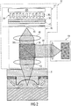
- Fig. 1 shows a device 10 with a molding tool 12, which comprises a molding surface 14 and is formed on a tool substrate 16. Laterally adjacent to the molding tool 12, membrane layers 18a and 18b are arranged on the tool substrate 16, which lie loosely against the tool substrate 16 in a channel region and terminate the channel region in a fluid-tight manner on the tool substrate. The fluid-tight sealed channel region thus forms channel structures 22a and 22b.
- the molding surface 14 may also include a coating to prevent the adhesion of molded materials to the molding tool 12.
- the molding tool 12 is positioned relative to a substrate 24 such that a region 26 is formed between a surface 25 of the substrate 24 and the molding tool 12, in which curable material 28 is arranged. Between the membrane structures 18a and 18b and the substrate is located adjacent to the region 26 further curable material 29, which is adapted to experience upon application of a pressure p 1 in the channel structures 22a and 22b a pressure.
- an irradiation unit 32 On the side facing away from the impression surface 14 of the molding tool 12, an irradiation unit 32 is arranged. It comprises a radiation source 34 which emits radiation 36. Radiation of radiation 36 is approximately parallel to each other at its origin. In a radiation direction, a gray filter 38 is arranged adjacent to and in the beam direction in front of a lens 42. The gray filter 38 is designed to attenuate a possibly excessive intensity of the radiation 36. In contrast, the diffuser 42 is formed to cancel collimation of the radiation 36 and to scatter the radiation 36.
- variable radiating surface 45 Adjacent to the diffuser 42 is a variable aperture 44 with a, formed by a variable opening diameter D1, variable radiating surface 45 is arranged.
- the variable radiating surface 45 is designed to allow a cone-shaped radiation 36b scattered by the diffusing screen 42 to emerge from the radiation source 34 with a cone width controlled by the variable opening diameter D1.
- an optical channel 46 is arranged which comprises a first beam-shaping optical element 48 and in a further course of the radiation direction a second beam-shaping optical element 52.
- the two beam-shaping optical elements 48 and 52 are designed such that they concentrate incident radiation.
- the first beam-shaping optical element 48 is designed and arranged such that the radiation 36b striking the first beam-shaping optical element 48 is collimated and the rays of the radiation 36b are approximately parallel to one another in the further course 36c. Due to the approximately parallel course of the rays in the radiation section 36c, the intensity of the radiation remains approximately constant over the course in the radiation direction.
- the radiation 36c is collimated by the second beam-shaping optical element 52 such that the intensity of the radiation increases in the section 36d by the bundling and in the region 26, in which the curable material 28 is arranged, neglecting absorption of the radiation by the curable material adjacent to the surface 25 has a local maximum.
- the local maximum of the intensity of the radiation 36 may, for example, also be positioned such that it is located between the impression surface 14 and the surface 25. In principle, the local maximum can be positioned at any axial location.
- Shrinkage of the curable material 28 induced by the radiation 36 may be compensated for by applying a pressure p 1 in the channel regions 22a and 22b such that the pressure p 1 in the channel structures 22a and 22b is at a pressure axially opposite to that in FIG Membrane structures 18a and 18b adjacent balancing areas with the other curable material 29 leads and a subsequent flow 54a-d of the further curable material 29 from the compensation area in the area 26 causes and closes by material shrinkage closes gaps.
- Compensation areas, in which the further curable material 29 is arranged are arranged such that the further curable material 29 undergoes no irradiation and thus remains uncured.
- the further curable material 29 can also be cured, for example by a complete opening of the diaphragm 44 or removed in a subsequent processing step, for example by a solvent.
- the two beam-shaping optical elements 48 and 52 By arranging the two beam-shaping optical elements 48 and 52, it is possible to adjust the radiation 36 entering the region 26 with great accuracy.
- the power of the radiation 36 can be controlled so accurately that the contour accuracy and thus the quality of molded lenses can be substantially increased.
- the diaphragm 44 is formed such that by adjusting the size of the radiating surface 45 of the variable diaphragm 44, the lateral extent of the area irradiated at one time is controllable, whereas the beam-shaping optical elements 48 and 52 are designed to control the degree of collimation of the radiation 36 and thus to allow a point with maximum radiation intensity.
- section 36c further optical elements for evaluating the radiation source and / or observing the curing zone may be arranged in region 26, as shown in the following exemplary embodiments.
- variable orifice 44 in combination with the beam-shaping optical elements 48 and 52, enables variable hardening of the curable material 28 along the surface 25 with precise adjustment of the curing zone by the beam-shaping optical elements 48 and 52.
- beam-forming optics expands the possibilities of controlling the curing process and allows a further improvement of the contour fidelity, since the polymer volume illuminated by the UV radiation and thus hardening can be optimally shaped in accordance with the achieved beam influence. It also allows the spatial separation of variable aperture and tool contour.
- tools and beam shaping optics are arranged side by side.
- sequential process control with a step & repeat machine, a single arrangement of tool and beam shaping optics is used.
- Fig. 1 1 shows an optical channel 46 with a two-lens path formed by the beam-shaping optical elements 48 and 52, which images the plane of the variable orifice 44 in the vicinity of the curing zone and thus in the vicinity of the substrate surface 25.
- Fig. 2 shows device 10 Fig. 1 in which a beam-splitting optical element in the form of a beam splitter cube 56 is arranged in the two-lobe beam path of the optical channel 46 and in the radiation direction between the first beam-shaping optical element 48 and the second beam-shaping optical element 52.
- the beam splitter cube 56 is configured to decouple a portion of the radiation 36c and arranged so that a decoupled portion 58 is directed onto an image surface of a camera 64.
- the camera 64 is designed to enable observation and evaluation of the emitted radiation 36.
- the evaluation may relate, for example, to the shape of the beam in section 36b or the degree of scattering of the radiation by the diffuser 42. It is also conceivable that the intensity of the radiation 36 can be monitored in this way.
- a differently shaped beam-splitting optical element such as a pelicle or a beam splitter plate, to decouple a portion of the radiation laterally from the beam splitting optical element 56 in the form of a beam splitter cube.
- Fig. 3 shows a device similar to device 10 in Fig. 2 in which the beam splitter cube 56 is arranged such that a portion of radiation reflected back from the molding tool or curing zone and the decoupled portion 58 'of the reflected radiation is directed onto the image surface of the camera 64' to allow observation of the curing zone.
- the beam splitting optical element 56 is shown as a beam splitter cube is analog Fig. 2
- Another conceivable embodiment of the beam-splitting element for example as a pelicle or as a beam splitter plate, conceivable.
- a monitoring and evaluation of the radiation source in combination with observation and evaluation of the curing zone a control or control circuit is constructed such that the radiation passing through the optical channel through the radiation source, the variable diaphragm or the beam-shaping optical elements is influenced, that the curing is optimized in a desired manner.
- an observed too rapid hardening can be compensated by a more strongly attenuating gray filter 38, so that the radiation intensity is reduced and thus the hardening is slowed down.
- Interventions in the curing process such as an adjustment of the radiation intensity can be done via an automated control or regulation, via the one Evaluation of the radiation source and / or the curing zone takes place.
- an observation and / or evaluation of the radiation source and / or the curing zone as well as the intervention in the curing process can be carried out manually by an operator.
- a camera for monitoring the curing zone or the radiation source is shown, other types of image sensors are possible, such as an intensity meter.
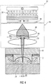
- Fig. 4 shows apparatus 10, wherein in the radiation direction between the first beam-shaping optical element 48 and the second beam-shaping optical element 52, a further variable aperture 66 is arranged.
- the further variable diaphragm 66 comprises an aperture 67 variable in size and lateral position with the variable diameter D2.
- variable diaphragm 66 is also designed to precisely adjust the lateral extent 68 in which the area 26 is irradiated by the radiation 36, since the irradiated area can be resolved laterally very precisely.
- Fig. 5 shows a device 10 analog Fig. 1 with a two-lens beam path in which microstructures 72 for locally adjusting the divergence of the illumination and diaphragm structures 74a and 74b for shielding areas 76a and 76b from irradiation are arranged on the substrate of the molding tool.
- Strongly directed irradiation of the curable material 28 may lead to the formation of refractive index gradients in the curable material 28, which may lead to streaking and hence deteriorated optical performance of the cured material.
- An avoidance of streaking can therefore be achieved by a diffuse irradiation.
- the use of the local microstructures 72 allows diffusion of incoming radiation and thus leads to locally increased divergence of the radiation, which avoids the formation of streaks.
- the transmitted light from the optics can be scattered locally and the directional effect of the upstream optics are partially or completely canceled.
- diffractive elements can also be arranged on the tool substrate for diffusion of the incoming radiation.
- These elements can be formed on one or both sides, continuously or discontinuously and can be arranged on one or more sides of the tool or of the tool substrate.
- the local diffusion elements may be disposed on the substrate to locally diverge radiation incident on the curable material through the substrate.
- the diaphragm structures 74a and 74b serve to shield regions 76a and 76b which are not intended to be cured during irradiation by the molding tool 12 or the tool substrate 16 or the membrane structures 18a, 18b.
- the aperture structures 74a and 74b shield the radiation 36 such that the channel-like shadows 76a and 76b are formed.
- the curable material 28 or further curable material 29 remains uncured during irradiation. After a curing or subsequent cleaning or development process, no cured material is disposed in these areas. These areas may then be used, for example, to enter a solvent or to dissolve soluble hardenable material to create air spaces.
- microstructures or diaphragm structures expands the field of application of beam-shaping devices in such a way that additional degrees of freedom with regard to the design as well as an increased quality of the molded structures can be achieved.
- Fig. 6a-c show schematic representations of a conversion of a variable aperture 44th
- a first aperture 78 having a plurality of apertures 79a-d is disposed opposite a second aperture 82 having a plurality of apertures 83a-d such that the apertures 79a-d and 83a-d comprise common optical axes 84a-d.
- the first aperture 78 and the second aperture 82 are identical.
- the first diaphragm 78 and the second diaphragm 82 form a common effective diaphragm 86.
- the effective diaphragm 86 comprises variable transmission regions 45a-d and the effective shadow regions 92a-e.
- FIG. 12 illustrates the effect on the effective aperture 86 when the first aperture 78 and the second aperture 82 are displaced from each other about the optical axes 84a-d.
- the aperture 78 becomes lateral to the optical axes 84a-d in one direction and the second aperture 82 also shifted laterally in an opposite direction, so arise opposite Fig. 6a reduced variable passage areas 45a-d and enlarged variable shadow areas 92a-e of the effective aperture 86, but the centers of the respective passage areas and thus the optical axes remain stationary.
- Fig. 6c shows that a displacement of the first aperture 78 and the second aperture 82 relative to each other in opposite directions laterally to the optical axes 84a-d can be performed so far that the entire area of the effective aperture 86 has the shadow area 92 and the variable passbands 45 a Have size of zero.
- the spacing of the apertures 79a-d and the apertures 83a-d, respectively, when producing a plurality or a field of structures, corresponds to the single or multiple of the distance of the structures or lenses to be produced.
- the apertures 79 and 83 can be z. B. have simple rectangular or round openings.
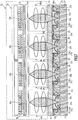
- Fig. 7 shows a device 20 comprising four impression tools 12a-d.
- the radiation source 34 is configured to provide the radiation 36.
- Adjacent to each curing region 26a-d, an optical channel 46a-d is arranged analogously to device 10.
- the variable aperture 44 has axially adjacent to the four optical channels 46a-d each have a variable radiating surface 45a-d.
- the variable gray filter 38 and the diffuser 42 are configured to filter and scatter the radiation 36 simultaneously for each of the four optical channels 46a-d.
- the diffuser 42 is configured to diffuse incident radiation 36 such that scattered radiation enters each of the four optical channels 46a-d.
- channel structures 22a-f are fluidly interconnected.
- the fluidic connection of the channel structures 22a-f results in that application of a pressure p 1 in one of the channel structures 22a-f also leads to formation of the pressure p 1 in the fluidically connected further channel structures.
- the impression tools 12a-d are arranged on the common tool substrate 16.
- the molding tools 12a-d are formed to mold the regions 26a-d on the substrate 24 with the surface 25.
- the impression tools are arranged on a common tool substrate and the regions 26a-d are molded on the surface of the common substrate, it is also possible for the tool substrate and / or the substrate to be formed from a plurality of individual components.
- hardened material 94a-e is arranged, which separates the areas 26a-d from each other such that further curable material 29 only in a laterally adjacent area 26a-d, but not in another compensation area can flow.
- the cured material 94a-e may be arranged such that between a step of disposing hardenable and further curable material 28 and 29 and irradiating the regions 26a-d, the further curable material may be in edge regions laterally spaced relative to the regions 26a-d the compensation areas, the further curable material 29 is cured.
- the formed axially to a plurality of optical channels and therefore large-area shaped radiation source 34 is formed so as to emit in the axially adjacent to the optical channels 46 a-d region of a collimated radiation.
- the diffusion plate 42 is formed to cancel out the collimation and to act respectively as a point radiation source with respect to the variable radiation surfaces 45a-d and the optical channels 46a-d subsequently arranged in the beam direction.
- an optical channel in each case comprises two beam-shaping optical elements, it is likewise conceivable for only one beam-shaping optical element or else a plurality of beam-shaping optical elements to be included in an optical channel.
- the beam-shaping optical elements 48 and 52 are represented as lenses in previous embodiments, it is also conceivable that the optical channel comprises one or more other beam-shaping optical elements, for example a prism, a diffractive structure or a Fresnel lens.
- the beam-shaping optical elements may be the same or different from each other, and optical channels may differ from each other in that different optical Channels comprise different beam-shaping optical elements.
- FIG. 12 shows a flowchart of a method 100 according to an embodiment of the present invention.
- the method 100 for producing a structure of curable material by molding comprises a first step 110 of arranging an impression tool 12 above a surface 25, for example a glass substrate, such that in a region 26 between the molding tool 12 and the surface 25 the curable material 28, For example, a UV polymer, on the surface 25 and the surface 25 facing molding surface 14 of the molding tool 12 adjacent and so that further curable material 29 can flow into the region 26.
- a UV polymer for example, on the surface 25 and the surface 25 facing molding surface 14 of the molding tool 12 adjacent and so that further curable material 29 can flow into the region 26.
- the method 100 comprises a second step 120 of the locally varying irradiation of the curable material 28 by means of a beam 36, which traverses an optical channel 46 arranged between a radiation source 34 and the molding tool 12 and beam collimating during the traversal, in the region, see FIG the hardenable material 28 laterally hardens at different rates along the surface 25 and shrinkages during hardening of the curable material 28 are compensated by the further curable material 29.
- a subsequent flow of the further curable material 29 into the region 26 can be induced, for example, by applying the pressure p 1 in the channel structures 22a and 22b and thus applying a pressure to the further curable material 29.
- the further curable material 29 is acted upon by a pressure from a lateral side in order to effect a subsequent flow of the further curable material 29 into the region 26. If the pressure p 1 is applied during the irradiation, then the further curable material 29 flows into the region 26 during the shrinkage.
- FIG. 9 shows a flowchart of a method 200 according to an embodiment of the present invention.
- the method 200 for producing a structure of curable material by molding comprises a first step 210 of arranging a molding tool 12 above a surface 25, for example a glass substrate, so that in a region 26 between the molding tool 12 and the surface 25 of the curable material 28 at the surface 25 and a surface facing the impression surface 14 of the molding tool 12 is adjacent and so that further curable material 29 can flow into the region 26.
- the method 200 comprises a second step 220 of locally varying irradiation of the curable material 28 by means of a beam 36 traversing an optical channel 46 disposed between the radiation source 34 and the molding tool 12 and beam-focused during traversal in the region such that the curable material 28 is lateral along the surface 25 cures at different rates, and shrinkages during curing of the curable material 28 are compensated by the further curable material 29, wherein the locally varying irradiation from one of the molding surface 14 opposite side of the molding tool 12 is performed through the molding tool 12 therethrough.
- an improvement of the curing process is, inter alia, an optimized production of micro-optical-electromechanical systems (MOEMS) by replication processes, such.
- MOEMS micro-optical-electromechanical systems
- optical elements are arranged per structure to be cured, which can be used to beam-shape the UV-curing UV radiation. Allow radiation.
- Fig. 10 shows a device for locally varying irradiation, according to the prior art.
- the device comprises the irradiation unit 32 and the molding tool 12, which is arranged on the tool substrate 16.
- the curable material 28 is arranged, wherein the mold opposite to the mold 12 facing surface 25 of the substrate 24 is arranged such that occurring during irradiation shrinkage in the curable material 28 by the Nachfie skill 54a and 54b of the further curable material 29 can be compensated.
- the optical channel 46 between the irradiation unit 32 and the substrate of the molding tool 16 does not comprise beam-shaping optical elements.
- the variable aperture 44 and the variable radiating surface 45 of diameter D1 are configured to confine the radiation 36 and thus allow for locally varying irradiation.
- this arrangement does not allow focusing of the radiation 36 in the curing zone or imaging of the radiation 36 or the curing zone in the region 26 onto a camera.
- the membrane structures 18a and 18b are arranged directly on the mold 12.
- the formation of the membrane structures 18a and 18b and the channel structures 22a and 22b and thus their function with respect to an application of external pressure to the further curable material 29 is identical.
- Fig. 11 shows an exemplary sequence of a sequential molding and curing process in a step & repeat machine
- the z. B. may be an adapted nanoimprint lithography device.
- a defined amount of polymer to be cured is deposited on the substrate so that a drop of polymer forms on the substrate.
- an impression tool is positioned on the drop, so that the drop firstly takes on the shape of the later lens and, on the other hand, can be positioned on the substrate with the molding tool.
- a step C the curing of the polymer by UV radiation, wherein the UV radiation, for example by a transparently designed molding tool or through the substrate can cause curing of the polymer.
- the impression tool is removed and positioned on an intermediate further drop of polymer to form the next lens. In this way, all lenses to be molded are gradually mounted on the substrate.
- the beam-splitting optical element can be arranged in the beam direction behind the at least first beam-shaping optical element.
- the beam-splitting optical element can be arranged in the beam direction in front of the at least first beam-shaping optical element.
- an aperture diaphragm which is variable in aperture size and / or lateral position can be arranged in a beam direction between the first and the second beam-shaping optical element.
- the locally varying irradiation may be carried out such that further curable material flows from a compensation area of the molding tool into the area which is not reached by a radiation with which the irradiation takes place.
Landscapes
- Health & Medical Sciences (AREA)
- Physics & Mathematics (AREA)
- Engineering & Computer Science (AREA)
- Thermal Sciences (AREA)
- Oral & Maxillofacial Surgery (AREA)
- Mechanical Engineering (AREA)
- Electromagnetism (AREA)
- Toxicology (AREA)
- Ophthalmology & Optometry (AREA)
- Manufacturing & Machinery (AREA)
- General Physics & Mathematics (AREA)
- Casting Or Compression Moulding Of Plastics Or The Like (AREA)
- Moulds For Moulding Plastics Or The Like (AREA)
Applications Claiming Priority (2)
| Application Number | Priority Date | Filing Date | Title |
|---|---|---|---|
| DE102013207243.0A DE102013207243B4 (de) | 2013-04-22 | 2013-04-22 | Vorrichtung und verfahren zur herstellung einer struktur aus aushärtbarem material durch abformung |
| PCT/EP2014/057064 WO2014173676A1 (de) | 2013-04-22 | 2014-04-08 | Vorrichtung und verfahren zur herstellung einer struktur aus aushärtbarem material durch abformung |
Publications (2)
| Publication Number | Publication Date |
|---|---|
| EP2988914A1 EP2988914A1 (de) | 2016-03-02 |
| EP2988914B1 true EP2988914B1 (de) | 2017-05-17 |
Family
ID=50478832
Family Applications (1)
| Application Number | Title | Priority Date | Filing Date |
|---|---|---|---|
| EP14716794.4A Active EP2988914B1 (de) | 2013-04-22 | 2014-04-08 | Vorrichtung und verfahren zur herstellung einer struktur aus aushärtbarem material durch abformung |
Country Status (7)
| Country | Link |
|---|---|
| US (1) | US11014269B2 (ko) |
| EP (1) | EP2988914B1 (ko) |
| JP (1) | JP6173565B2 (ko) |
| KR (1) | KR101858486B1 (ko) |
| CN (1) | CN105263686B (ko) |
| DE (1) | DE102013207243B4 (ko) |
| WO (1) | WO2014173676A1 (ko) |
Families Citing this family (3)
| Publication number | Priority date | Publication date | Assignee | Title |
|---|---|---|---|---|
| CA3076669A1 (en) | 2017-10-17 | 2019-04-25 | Magic Leap, Inc. | Methods and apparatuses for casting polymer products |
| EP3756226B1 (en) * | 2018-02-19 | 2021-10-27 | Signify Holding B.V. | Sealed device with light engine |
| US11009661B2 (en) * | 2018-10-16 | 2021-05-18 | Magic Leap, Inc. | Methods and apparatuses for casting polymer products |
Family Cites Families (30)
| Publication number | Priority date | Publication date | Assignee | Title |
|---|---|---|---|---|
| US3848970A (en) * | 1973-09-07 | 1974-11-19 | Westinghouse Electric Corp | Apparatus for measuring and controlling annulus diameters of images formed by a pincushion lens |
| US4398824A (en) * | 1981-04-15 | 1983-08-16 | Bell Telephone Laboratories, Incorporated | Wafer tilt compensation in zone plate alignment system |
| US4750822A (en) * | 1986-03-28 | 1988-06-14 | Therma-Wave, Inc. | Method and apparatus for optically detecting surface states in materials |
| JPH01163027A (ja) * | 1987-12-21 | 1989-06-27 | Matsushita Electric Ind Co Ltd | 光学素子の成形方法およびその装置 |
| US5340992A (en) * | 1988-02-16 | 1994-08-23 | Canon Kabushiki Kaisha | Apparatus and method of detecting positional relationship using a weighted coefficient |
| FR2651074B1 (fr) | 1989-08-16 | 1991-11-29 | Sgs Thomson Microelectronics | Circuit d'amplification a impedance d'entree determinee et a differentes valeurs de transconductance |
| US6800225B1 (en) | 1994-07-14 | 2004-10-05 | Novartis Ag | Process and device for the manufacture of mouldings and mouldings manufactured in accordance with that process |
| SG49612A1 (en) * | 1993-07-19 | 2003-03-18 | Novartis Ag | A process and device for the manufacture of moulding and mouldings manufactured in accordance with that process |
| US6022498A (en) * | 1996-04-19 | 2000-02-08 | Q2100, Inc. | Methods for eyeglass lens curing using ultraviolet light |
| JP3825505B2 (ja) * | 1996-08-20 | 2006-09-27 | ペンタックス株式会社 | 複合化レンズの製造方法 |
| US6696008B2 (en) * | 2000-05-25 | 2004-02-24 | Westar Photonics Inc. | Maskless laser beam patterning ablation of multilayered structures with continuous monitoring of ablation |
| US6954275B2 (en) * | 2000-08-01 | 2005-10-11 | Boards Of Regents, The University Of Texas System | Methods for high-precision gap and orientation sensing between a transparent template and substrate for imprint lithography |
| US20020190207A1 (en) * | 2000-09-20 | 2002-12-19 | Ady Levy | Methods and systems for determining a characteristic of micro defects on a specimen |
| JP4096565B2 (ja) * | 2002-01-28 | 2008-06-04 | 富士ゼロックス株式会社 | マイクロレンズアレーの製造方法、それに用いる電解液および製造装置 |
| JP3941604B2 (ja) * | 2002-06-26 | 2007-07-04 | 富士ゼロックス株式会社 | マイクロレンズアレーの製造方法、それに用いる電解液およびマイクロレンズアレー樹脂材料、ならびに原盤製造装置 |
| JP4574240B2 (ja) * | 2004-06-11 | 2010-11-04 | キヤノン株式会社 | 加工装置、加工方法、デバイス製造方法 |
| JP4515853B2 (ja) * | 2004-08-04 | 2010-08-04 | ナブテスコ株式会社 | 光学的立体造形装置 |
| JP4515413B2 (ja) * | 2005-05-27 | 2010-07-28 | エーエスエムエル ネザーランズ ビー.ブイ. | インプリントリソグラフィ |
| US7708924B2 (en) * | 2005-07-21 | 2010-05-04 | Asml Netherlands B.V. | Imprint lithography |
| JP2007081070A (ja) * | 2005-09-14 | 2007-03-29 | Canon Inc | 加工装置及び方法 |
| WO2007121208A2 (en) * | 2006-04-11 | 2007-10-25 | Massachusetts Institute Of Technology | Nanometer-precision tip-to-substrate control and pattern registration for scanning-probe lithography |
| JP2007313768A (ja) * | 2006-05-26 | 2007-12-06 | Olympus Corp | 複合光学素子の製造方法、複合光学素子の成形装置 |
| JP2008030423A (ja) * | 2006-08-01 | 2008-02-14 | Nikon Corp | 光学素子製造方法及び導光板 |
| JP2008158183A (ja) * | 2006-12-22 | 2008-07-10 | Sony Corp | 光学素子の製造方法 |
| KR100938643B1 (ko) | 2007-11-27 | 2010-01-28 | 주식회사 옵토메카 | 복합렌즈 성형장치 및 방법 |
| JP5267174B2 (ja) * | 2009-02-03 | 2013-08-21 | ソニー株式会社 | 光造形装置及び造形ベース |
| DE102009055080B4 (de) * | 2009-12-21 | 2019-11-14 | Fraunhofer-Gesellschaft zur Förderung der angewandten Forschung e.V. | Verfahren und Vorrichtung zum Herstellen einer Struktur, Abformwerkzeug |
| DE102010030138A1 (de) * | 2010-06-15 | 2011-12-15 | Fraunhofer-Gesellschaft zur Förderung der angewandten Forschung e.V. | Projektionsdisplay und Verfahren zum Anzeigen eines Gesamtbilds |
| US9396710B2 (en) | 2011-02-25 | 2016-07-19 | Pipe Makers Union, Llc | Fipple (mouthpiece) for a wind musical instrument and method of making a fipple for a wind musical instrument |
| JP5637931B2 (ja) * | 2011-05-17 | 2014-12-10 | キヤノン株式会社 | インプリント装置、インプリント方法およびデバイス製造方法 |
-
2013
- 2013-04-22 DE DE102013207243.0A patent/DE102013207243B4/de not_active Expired - Fee Related
-
2014
- 2014-04-08 EP EP14716794.4A patent/EP2988914B1/de active Active
- 2014-04-08 WO PCT/EP2014/057064 patent/WO2014173676A1/de active Application Filing
- 2014-04-08 KR KR1020157033048A patent/KR101858486B1/ko active IP Right Grant
- 2014-04-08 CN CN201480023048.2A patent/CN105263686B/zh active Active
- 2014-04-08 JP JP2016509363A patent/JP6173565B2/ja not_active Expired - Fee Related
-
2015
- 2015-10-21 US US14/919,636 patent/US11014269B2/en active Active
Also Published As
| Publication number | Publication date |
|---|---|
| CN105263686A (zh) | 2016-01-20 |
| JP2016518274A (ja) | 2016-06-23 |
| US20160039122A1 (en) | 2016-02-11 |
| CN105263686B (zh) | 2017-10-17 |
| DE102013207243A1 (de) | 2014-10-23 |
| KR20150144798A (ko) | 2015-12-28 |
| JP6173565B2 (ja) | 2017-08-02 |
| EP2988914A1 (de) | 2016-03-02 |
| US11014269B2 (en) | 2021-05-25 |
| KR101858486B1 (ko) | 2018-05-16 |
| WO2014173676A1 (de) | 2014-10-30 |
| DE102013207243B4 (de) | 2019-10-02 |
Similar Documents
| Publication | Publication Date | Title |
|---|---|---|
| DE102009055080B4 (de) | Verfahren und Vorrichtung zum Herstellen einer Struktur, Abformwerkzeug | |
| EP3282181A1 (de) | Mikrooptic - linsen auf glas mit gedruckter strahlenblende - konzept und herstellverfahren | |
| DE102010040768A1 (de) | Spektralzerlegungsvorrichtung und Herstellung derselben | |
| DE102013209246B4 (de) | Verfahren zur Herstellung einer falschlichtunterdrückenden Struktur und Vorrichtung mit derselben | |
| EP2988914B1 (de) | Vorrichtung und verfahren zur herstellung einer struktur aus aushärtbarem material durch abformung | |
| WO2010130415A1 (de) | Vorrichtung zur formung von laserstrahlung sowie laservorrichtung mit einer derartigen vorrichtung | |
| EP3162549B1 (de) | Verfahren und vorrichtung zur herstellung eines optischen elements mit zumindest einem funktionalen bereich, sowie verwendung der vorrichtung | |
| DE102007022895B9 (de) | Vorrichtung zum Übertragen von in einer Maske vorgesehenen Strukturen auf ein Substrat | |
| EP2855131B1 (de) | Verfahren und vorrichtung zum herstellen einer vielzahl von mikrolinsen | |
| EP3414625B1 (de) | Vorrichtung und verfahren zur moiré-vermessung eines optischen prüflings | |
| DE102019120954B4 (de) | Verfahren zur Herstellung einer Klebeverbindung, Trägerplatte für die Herstellung einer Klebeverbindung und Klebevorrichtung zur Herstellung einer Klebeverbindung | |
| DE102016124420A1 (de) | Linsenanordnung, insbesondere Brillenglasanordnung, und Verfahren zum Herstellen einer Linsenanordnung | |
| DE102015224522B4 (de) | Beleuchtungssystem einer mikrolithographischen Projektionsanlage und Verfahren zum Betreiben eines solchen Systems | |
| DE102021202164B3 (de) | Tandemblendenarchitektur zur Füllfaktorerhöhung von kompakten Multikanalabbildungssystemen | |
| DE102014105851B3 (de) | Verfahren zur Herstellung einer optischen Baueinheit | |
| WO2022106138A1 (de) | Vorrichtung zum erzeugen einer definierten laserbeleuchtung auf einer arbeitsebene | |
| DE102013111744A1 (de) | Elektronenstrahl-Belichtungsverfahren | |
| DE102022108300A1 (de) | Vorrichtung zum Erzeugen einer definierten Laserlinie auf einer Arbeitsebene | |
| DE102014215218A1 (de) | Stereolithografieeinheit mit homogenisiertem Strahlengang | |
| DE102017212130A1 (de) | Auskoppelelement für einen Lichtleiter zur Lichtführung an einem Lichtlaufzeitsensor | |
| DE102011004494A1 (de) | Variabler Filter | |
| DE102015211579A1 (de) | Linsenartige optische Bauelemente | |
| DE102013203751A1 (de) | Beleuchtungssystem einer mikrolithographischen projektionsbelichtungsanlage | |
| DE102012212394A1 (de) | Abtrennvorrichtung und abtrennverfahren für projektionsbelichtungsanlagen |
Legal Events
| Date | Code | Title | Description |
|---|---|---|---|
| PUAI | Public reference made under article 153(3) epc to a published international application that has entered the european phase |
Free format text: ORIGINAL CODE: 0009012 |
|
| 17P | Request for examination filed |
Effective date: 20151019 |
|
| AK | Designated contracting states |
Kind code of ref document: A1 Designated state(s): AL AT BE BG CH CY CZ DE DK EE ES FI FR GB GR HR HU IE IS IT LI LT LU LV MC MK MT NL NO PL PT RO RS SE SI SK SM TR |
|
| AX | Request for extension of the european patent |
Extension state: BA ME |
|
| DAX | Request for extension of the european patent (deleted) | ||
| GRAP | Despatch of communication of intention to grant a patent |
Free format text: ORIGINAL CODE: EPIDOSNIGR1 |
|
| RIC1 | Information provided on ipc code assigned before grant |
Ipc: B29K 101/00 20060101ALN20161103BHEP Ipc: B29C 35/08 20060101AFI20161103BHEP Ipc: B29C 35/02 20060101ALI20161103BHEP Ipc: B29C 43/58 20060101ALN20161103BHEP Ipc: B29K 105/24 20060101ALN20161103BHEP Ipc: B29C 43/00 20060101ALI20161103BHEP Ipc: B29C 37/00 20060101ALI20161103BHEP Ipc: B29D 11/00 20060101ALI20161103BHEP Ipc: B29C 43/32 20060101ALI20161103BHEP |
|
| RAP1 | Party data changed (applicant data changed or rights of an application transferred) |
Owner name: FRAUNHOFER-GESELLSCHAFT ZUR FOERDERUNG DER ANGEWAN |
|
| INTG | Intention to grant announced |
Effective date: 20161130 |
|
| GRAS | Grant fee paid |
Free format text: ORIGINAL CODE: EPIDOSNIGR3 |
|
| GRAA | (expected) grant |
Free format text: ORIGINAL CODE: 0009210 |
|
| AK | Designated contracting states |
Kind code of ref document: B1 Designated state(s): AL AT BE BG CH CY CZ DE DK EE ES FI FR GB GR HR HU IE IS IT LI LT LU LV MC MK MT NL NO PL PT RO RS SE SI SK SM TR |
|
| REG | Reference to a national code |
Ref country code: GB Ref legal event code: FG4D Free format text: NOT ENGLISH |
|
| REG | Reference to a national code |
Ref country code: CH Ref legal event code: EP |
|
| REG | Reference to a national code |
Ref country code: IE Ref legal event code: FG4D Free format text: LANGUAGE OF EP DOCUMENT: GERMAN |
|
| REG | Reference to a national code |
Ref country code: AT Ref legal event code: REF Ref document number: 894064 Country of ref document: AT Kind code of ref document: T Effective date: 20170615 |
|
| REG | Reference to a national code |
Ref country code: DE Ref legal event code: R096 Ref document number: 502014003875 Country of ref document: DE |
|
| REG | Reference to a national code |
Ref country code: NL Ref legal event code: FP |
|
| REG | Reference to a national code |
Ref country code: LT Ref legal event code: MG4D |
|
| PG25 | Lapsed in a contracting state [announced via postgrant information from national office to epo] |
Ref country code: GR Free format text: LAPSE BECAUSE OF FAILURE TO SUBMIT A TRANSLATION OF THE DESCRIPTION OR TO PAY THE FEE WITHIN THE PRESCRIBED TIME-LIMIT Effective date: 20170818 Ref country code: LT Free format text: LAPSE BECAUSE OF FAILURE TO SUBMIT A TRANSLATION OF THE DESCRIPTION OR TO PAY THE FEE WITHIN THE PRESCRIBED TIME-LIMIT Effective date: 20170517 Ref country code: HR Free format text: LAPSE BECAUSE OF FAILURE TO SUBMIT A TRANSLATION OF THE DESCRIPTION OR TO PAY THE FEE WITHIN THE PRESCRIBED TIME-LIMIT Effective date: 20170517 Ref country code: NO Free format text: LAPSE BECAUSE OF FAILURE TO SUBMIT A TRANSLATION OF THE DESCRIPTION OR TO PAY THE FEE WITHIN THE PRESCRIBED TIME-LIMIT Effective date: 20170817 Ref country code: ES Free format text: LAPSE BECAUSE OF FAILURE TO SUBMIT A TRANSLATION OF THE DESCRIPTION OR TO PAY THE FEE WITHIN THE PRESCRIBED TIME-LIMIT Effective date: 20170517 |
|
| PG25 | Lapsed in a contracting state [announced via postgrant information from national office to epo] |
Ref country code: LV Free format text: LAPSE BECAUSE OF FAILURE TO SUBMIT A TRANSLATION OF THE DESCRIPTION OR TO PAY THE FEE WITHIN THE PRESCRIBED TIME-LIMIT Effective date: 20170517 Ref country code: RS Free format text: LAPSE BECAUSE OF FAILURE TO SUBMIT A TRANSLATION OF THE DESCRIPTION OR TO PAY THE FEE WITHIN THE PRESCRIBED TIME-LIMIT Effective date: 20170517 Ref country code: IS Free format text: LAPSE BECAUSE OF FAILURE TO SUBMIT A TRANSLATION OF THE DESCRIPTION OR TO PAY THE FEE WITHIN THE PRESCRIBED TIME-LIMIT Effective date: 20170917 Ref country code: PL Free format text: LAPSE BECAUSE OF FAILURE TO SUBMIT A TRANSLATION OF THE DESCRIPTION OR TO PAY THE FEE WITHIN THE PRESCRIBED TIME-LIMIT Effective date: 20170517 Ref country code: BG Free format text: LAPSE BECAUSE OF FAILURE TO SUBMIT A TRANSLATION OF THE DESCRIPTION OR TO PAY THE FEE WITHIN THE PRESCRIBED TIME-LIMIT Effective date: 20170817 Ref country code: SE Free format text: LAPSE BECAUSE OF FAILURE TO SUBMIT A TRANSLATION OF THE DESCRIPTION OR TO PAY THE FEE WITHIN THE PRESCRIBED TIME-LIMIT Effective date: 20170517 |
|
| PG25 | Lapsed in a contracting state [announced via postgrant information from national office to epo] |
Ref country code: EE Free format text: LAPSE BECAUSE OF FAILURE TO SUBMIT A TRANSLATION OF THE DESCRIPTION OR TO PAY THE FEE WITHIN THE PRESCRIBED TIME-LIMIT Effective date: 20170517 Ref country code: DK Free format text: LAPSE BECAUSE OF FAILURE TO SUBMIT A TRANSLATION OF THE DESCRIPTION OR TO PAY THE FEE WITHIN THE PRESCRIBED TIME-LIMIT Effective date: 20170517 Ref country code: CZ Free format text: LAPSE BECAUSE OF FAILURE TO SUBMIT A TRANSLATION OF THE DESCRIPTION OR TO PAY THE FEE WITHIN THE PRESCRIBED TIME-LIMIT Effective date: 20170517 Ref country code: SK Free format text: LAPSE BECAUSE OF FAILURE TO SUBMIT A TRANSLATION OF THE DESCRIPTION OR TO PAY THE FEE WITHIN THE PRESCRIBED TIME-LIMIT Effective date: 20170517 Ref country code: RO Free format text: LAPSE BECAUSE OF FAILURE TO SUBMIT A TRANSLATION OF THE DESCRIPTION OR TO PAY THE FEE WITHIN THE PRESCRIBED TIME-LIMIT Effective date: 20170517 |
|
| REG | Reference to a national code |
Ref country code: DE Ref legal event code: R097 Ref document number: 502014003875 Country of ref document: DE |
|
| PG25 | Lapsed in a contracting state [announced via postgrant information from national office to epo] |
Ref country code: SM Free format text: LAPSE BECAUSE OF FAILURE TO SUBMIT A TRANSLATION OF THE DESCRIPTION OR TO PAY THE FEE WITHIN THE PRESCRIBED TIME-LIMIT Effective date: 20170517 |
|
| PLBE | No opposition filed within time limit |
Free format text: ORIGINAL CODE: 0009261 |
|
| STAA | Information on the status of an ep patent application or granted ep patent |
Free format text: STATUS: NO OPPOSITION FILED WITHIN TIME LIMIT |
|
| REG | Reference to a national code |
Ref country code: FR Ref legal event code: PLFP Year of fee payment: 5 |
|
| 26N | No opposition filed |
Effective date: 20180220 |
|
| PG25 | Lapsed in a contracting state [announced via postgrant information from national office to epo] |
Ref country code: SI Free format text: LAPSE BECAUSE OF FAILURE TO SUBMIT A TRANSLATION OF THE DESCRIPTION OR TO PAY THE FEE WITHIN THE PRESCRIBED TIME-LIMIT Effective date: 20170517 |
|
| PG25 | Lapsed in a contracting state [announced via postgrant information from national office to epo] |
Ref country code: MT Free format text: LAPSE BECAUSE OF FAILURE TO SUBMIT A TRANSLATION OF THE DESCRIPTION OR TO PAY THE FEE WITHIN THE PRESCRIBED TIME-LIMIT Effective date: 20170517 |
|
| PG25 | Lapsed in a contracting state [announced via postgrant information from national office to epo] |
Ref country code: MC Free format text: LAPSE BECAUSE OF FAILURE TO SUBMIT A TRANSLATION OF THE DESCRIPTION OR TO PAY THE FEE WITHIN THE PRESCRIBED TIME-LIMIT Effective date: 20170517 |
|
| REG | Reference to a national code |
Ref country code: CH Ref legal event code: PL |
|
| REG | Reference to a national code |
Ref country code: BE Ref legal event code: MM Effective date: 20180430 |
|
| REG | Reference to a national code |
Ref country code: IE Ref legal event code: MM4A |
|
| PG25 | Lapsed in a contracting state [announced via postgrant information from national office to epo] |
Ref country code: LU Free format text: LAPSE BECAUSE OF NON-PAYMENT OF DUE FEES Effective date: 20180408 |
|
| PG25 | Lapsed in a contracting state [announced via postgrant information from national office to epo] |
Ref country code: BE Free format text: LAPSE BECAUSE OF NON-PAYMENT OF DUE FEES Effective date: 20180430 Ref country code: LI Free format text: LAPSE BECAUSE OF NON-PAYMENT OF DUE FEES Effective date: 20180430 Ref country code: CH Free format text: LAPSE BECAUSE OF NON-PAYMENT OF DUE FEES Effective date: 20180430 |
|
| PG25 | Lapsed in a contracting state [announced via postgrant information from national office to epo] |
Ref country code: IE Free format text: LAPSE BECAUSE OF NON-PAYMENT OF DUE FEES Effective date: 20180408 |
|
| PG25 | Lapsed in a contracting state [announced via postgrant information from national office to epo] |
Ref country code: TR Free format text: LAPSE BECAUSE OF FAILURE TO SUBMIT A TRANSLATION OF THE DESCRIPTION OR TO PAY THE FEE WITHIN THE PRESCRIBED TIME-LIMIT Effective date: 20170517 |
|
| PG25 | Lapsed in a contracting state [announced via postgrant information from national office to epo] |
Ref country code: PT Free format text: LAPSE BECAUSE OF FAILURE TO SUBMIT A TRANSLATION OF THE DESCRIPTION OR TO PAY THE FEE WITHIN THE PRESCRIBED TIME-LIMIT Effective date: 20170517 |
|
| PG25 | Lapsed in a contracting state [announced via postgrant information from national office to epo] |
Ref country code: HU Free format text: LAPSE BECAUSE OF FAILURE TO SUBMIT A TRANSLATION OF THE DESCRIPTION OR TO PAY THE FEE WITHIN THE PRESCRIBED TIME-LIMIT; INVALID AB INITIO Effective date: 20140408 Ref country code: MK Free format text: LAPSE BECAUSE OF NON-PAYMENT OF DUE FEES Effective date: 20170517 Ref country code: CY Free format text: LAPSE BECAUSE OF FAILURE TO SUBMIT A TRANSLATION OF THE DESCRIPTION OR TO PAY THE FEE WITHIN THE PRESCRIBED TIME-LIMIT Effective date: 20170517 |
|
| PG25 | Lapsed in a contracting state [announced via postgrant information from national office to epo] |
Ref country code: AL Free format text: LAPSE BECAUSE OF FAILURE TO SUBMIT A TRANSLATION OF THE DESCRIPTION OR TO PAY THE FEE WITHIN THE PRESCRIBED TIME-LIMIT Effective date: 20170517 |
|
| REG | Reference to a national code |
Ref country code: AT Ref legal event code: MM01 Ref document number: 894064 Country of ref document: AT Kind code of ref document: T Effective date: 20190408 |
|
| PG25 | Lapsed in a contracting state [announced via postgrant information from national office to epo] |
Ref country code: AT Free format text: LAPSE BECAUSE OF NON-PAYMENT OF DUE FEES Effective date: 20190408 |
|
| PGFP | Annual fee paid to national office [announced via postgrant information from national office to epo] |
Ref country code: IT Payment date: 20210430 Year of fee payment: 8 Ref country code: FI Payment date: 20210420 Year of fee payment: 8 |
|
| PGFP | Annual fee paid to national office [announced via postgrant information from national office to epo] |
Ref country code: NL Payment date: 20210421 Year of fee payment: 8 |
|
| REG | Reference to a national code |
Ref country code: NL Ref legal event code: MM Effective date: 20220501 |
|
| PG25 | Lapsed in a contracting state [announced via postgrant information from national office to epo] |
Ref country code: NL Free format text: LAPSE BECAUSE OF NON-PAYMENT OF DUE FEES Effective date: 20220501 Ref country code: FI Free format text: LAPSE BECAUSE OF NON-PAYMENT OF DUE FEES Effective date: 20220408 |
|
| PG25 | Lapsed in a contracting state [announced via postgrant information from national office to epo] |
Ref country code: IT Free format text: LAPSE BECAUSE OF NON-PAYMENT OF DUE FEES Effective date: 20220408 |
|
| P01 | Opt-out of the competence of the unified patent court (upc) registered |
Effective date: 20230524 |
|
| PGFP | Annual fee paid to national office [announced via postgrant information from national office to epo] |
Ref country code: FR Payment date: 20230417 Year of fee payment: 10 Ref country code: DE Payment date: 20230418 Year of fee payment: 10 |
|
| PGFP | Annual fee paid to national office [announced via postgrant information from national office to epo] |
Ref country code: GB Payment date: 20230420 Year of fee payment: 10 |