EP2988416B1 - Circuits and methods for 2g amplification using 3g/4g linear path combination - Google Patents
Circuits and methods for 2g amplification using 3g/4g linear path combination Download PDFInfo
- Publication number
- EP2988416B1 EP2988416B1 EP15181220.3A EP15181220A EP2988416B1 EP 2988416 B1 EP2988416 B1 EP 2988416B1 EP 15181220 A EP15181220 A EP 15181220A EP 2988416 B1 EP2988416 B1 EP 2988416B1
- Authority
- EP
- European Patent Office
- Prior art keywords
- amplification
- signal
- path
- end architecture
- paths
- Prior art date
- Legal status (The legal status is an assumption and is not a legal conclusion. Google has not performed a legal analysis and makes no representation as to the accuracy of the status listed.)
- Active
Links
Images


Classifications
-
- H—ELECTRICITY
- H03—ELECTRONIC CIRCUITRY
- H03F—AMPLIFIERS
- H03F1/00—Details of amplifiers with only discharge tubes, only semiconductor devices or only unspecified devices as amplifying elements
- H03F1/02—Modifications of amplifiers to raise the efficiency, e.g. gliding Class A stages, use of an auxiliary oscillation
- H03F1/0205—Modifications of amplifiers to raise the efficiency, e.g. gliding Class A stages, use of an auxiliary oscillation in transistor amplifiers
- H03F1/0277—Selecting one or more amplifiers from a plurality of amplifiers
-
- H—ELECTRICITY
- H03—ELECTRONIC CIRCUITRY
- H03F—AMPLIFIERS
- H03F3/00—Amplifiers with only discharge tubes or only semiconductor devices as amplifying elements
- H03F3/189—High-frequency amplifiers, e.g. radio frequency amplifiers
- H03F3/19—High-frequency amplifiers, e.g. radio frequency amplifiers with semiconductor devices only
- H03F3/191—Tuned amplifiers
-
- H—ELECTRICITY
- H03—ELECTRONIC CIRCUITRY
- H03F—AMPLIFIERS
- H03F3/00—Amplifiers with only discharge tubes or only semiconductor devices as amplifying elements
- H03F3/189—High-frequency amplifiers, e.g. radio frequency amplifiers
- H03F3/19—High-frequency amplifiers, e.g. radio frequency amplifiers with semiconductor devices only
- H03F3/195—High-frequency amplifiers, e.g. radio frequency amplifiers with semiconductor devices only in integrated circuits
-
- H—ELECTRICITY
- H03—ELECTRONIC CIRCUITRY
- H03F—AMPLIFIERS
- H03F3/00—Amplifiers with only discharge tubes or only semiconductor devices as amplifying elements
- H03F3/20—Power amplifiers, e.g. Class B amplifiers, Class C amplifiers
- H03F3/21—Power amplifiers, e.g. Class B amplifiers, Class C amplifiers with semiconductor devices only
- H03F3/211—Power amplifiers, e.g. Class B amplifiers, Class C amplifiers with semiconductor devices only using a combination of several amplifiers
-
- H—ELECTRICITY
- H03—ELECTRONIC CIRCUITRY
- H03F—AMPLIFIERS
- H03F3/00—Amplifiers with only discharge tubes or only semiconductor devices as amplifying elements
- H03F3/20—Power amplifiers, e.g. Class B amplifiers, Class C amplifiers
- H03F3/21—Power amplifiers, e.g. Class B amplifiers, Class C amplifiers with semiconductor devices only
- H03F3/213—Power amplifiers, e.g. Class B amplifiers, Class C amplifiers with semiconductor devices only in integrated circuits
-
- H—ELECTRICITY
- H03—ELECTRONIC CIRCUITRY
- H03F—AMPLIFIERS
- H03F3/00—Amplifiers with only discharge tubes or only semiconductor devices as amplifying elements
- H03F3/20—Power amplifiers, e.g. Class B amplifiers, Class C amplifiers
- H03F3/24—Power amplifiers, e.g. Class B amplifiers, Class C amplifiers of transmitter output stages
- H03F3/245—Power amplifiers, e.g. Class B amplifiers, Class C amplifiers of transmitter output stages with semiconductor devices only
-
- H—ELECTRICITY
- H03—ELECTRONIC CIRCUITRY
- H03F—AMPLIFIERS
- H03F3/00—Amplifiers with only discharge tubes or only semiconductor devices as amplifying elements
- H03F3/72—Gated amplifiers, i.e. amplifiers which are rendered operative or inoperative by means of a control signal
-
- H—ELECTRICITY
- H04—ELECTRIC COMMUNICATION TECHNIQUE
- H04B—TRANSMISSION
- H04B1/00—Details of transmission systems, not covered by a single one of groups H04B3/00 - H04B13/00; Details of transmission systems not characterised by the medium used for transmission
- H04B1/005—Details of transmission systems, not covered by a single one of groups H04B3/00 - H04B13/00; Details of transmission systems not characterised by the medium used for transmission adapting radio receivers, transmitters andtransceivers for operation on two or more bands, i.e. frequency ranges
- H04B1/0053—Details of transmission systems, not covered by a single one of groups H04B3/00 - H04B13/00; Details of transmission systems not characterised by the medium used for transmission adapting radio receivers, transmitters andtransceivers for operation on two or more bands, i.e. frequency ranges with common antenna for more than one band
-
- H—ELECTRICITY
- H04—ELECTRIC COMMUNICATION TECHNIQUE
- H04B—TRANSMISSION
- H04B1/00—Details of transmission systems, not covered by a single one of groups H04B3/00 - H04B13/00; Details of transmission systems not characterised by the medium used for transmission
- H04B1/06—Receivers
- H04B1/16—Circuits
- H04B1/18—Input circuits, e.g. for coupling to an antenna or a transmission line
-
- H—ELECTRICITY
- H04—ELECTRIC COMMUNICATION TECHNIQUE
- H04B—TRANSMISSION
- H04B1/00—Details of transmission systems, not covered by a single one of groups H04B3/00 - H04B13/00; Details of transmission systems not characterised by the medium used for transmission
- H04B1/38—Transceivers, i.e. devices in which transmitter and receiver form a structural unit and in which at least one part is used for functions of transmitting and receiving
- H04B1/40—Circuits
- H04B1/401—Circuits for selecting or indicating operating mode
-
- H—ELECTRICITY
- H03—ELECTRONIC CIRCUITRY
- H03F—AMPLIFIERS
- H03F2200/00—Indexing scheme relating to amplifiers
- H03F2200/111—Indexing scheme relating to amplifiers the amplifier being a dual or triple band amplifier, e.g. 900 and 1800 MHz, e.g. switched or not switched, simultaneously or not
-
- H—ELECTRICITY
- H03—ELECTRONIC CIRCUITRY
- H03F—AMPLIFIERS
- H03F2200/00—Indexing scheme relating to amplifiers
- H03F2200/225—Indexing scheme relating to amplifiers the input circuit of an amplifying stage comprising an LC-network
-
- H—ELECTRICITY
- H03—ELECTRONIC CIRCUITRY
- H03F—AMPLIFIERS
- H03F2200/00—Indexing scheme relating to amplifiers
- H03F2200/231—Indexing scheme relating to amplifiers the input of an amplifier can be switched on or off by a switch to amplify or not an input signal
-
- H—ELECTRICITY
- H03—ELECTRONIC CIRCUITRY
- H03F—AMPLIFIERS
- H03F2200/00—Indexing scheme relating to amplifiers
- H03F2200/451—Indexing scheme relating to amplifiers the amplifier being a radio frequency amplifier
-
- H—ELECTRICITY
- H03—ELECTRONIC CIRCUITRY
- H03F—AMPLIFIERS
- H03F2200/00—Indexing scheme relating to amplifiers
- H03F2200/541—Transformer coupled at the output of an amplifier
-
- H—ELECTRICITY
- H03—ELECTRONIC CIRCUITRY
- H03F—AMPLIFIERS
- H03F2203/00—Indexing scheme relating to amplifiers with only discharge tubes or only semiconductor devices as amplifying elements covered by H03F3/00
- H03F2203/20—Indexing scheme relating to power amplifiers, e.g. Class B amplifiers, Class C amplifiers
- H03F2203/21—Indexing scheme relating to power amplifiers, e.g. Class B amplifiers, Class C amplifiers with semiconductor devices only
- H03F2203/211—Indexing scheme relating to power amplifiers, e.g. Class B amplifiers, Class C amplifiers with semiconductor devices only using a combination of several amplifiers
- H03F2203/21109—An input signal being distributed by switching to a plurality of paralleled power amplifiers
-
- H—ELECTRICITY
- H03—ELECTRONIC CIRCUITRY
- H03F—AMPLIFIERS
- H03F2203/00—Indexing scheme relating to amplifiers with only discharge tubes or only semiconductor devices as amplifying elements covered by H03F3/00
- H03F2203/20—Indexing scheme relating to power amplifiers, e.g. Class B amplifiers, Class C amplifiers
- H03F2203/21—Indexing scheme relating to power amplifiers, e.g. Class B amplifiers, Class C amplifiers with semiconductor devices only
- H03F2203/211—Indexing scheme relating to power amplifiers, e.g. Class B amplifiers, Class C amplifiers with semiconductor devices only using a combination of several amplifiers
- H03F2203/21139—An impedance adaptation circuit being added at the output of a power amplifier stage
-
- H—ELECTRICITY
- H03—ELECTRONIC CIRCUITRY
- H03F—AMPLIFIERS
- H03F2203/00—Indexing scheme relating to amplifiers with only discharge tubes or only semiconductor devices as amplifying elements covered by H03F3/00
- H03F2203/20—Indexing scheme relating to power amplifiers, e.g. Class B amplifiers, Class C amplifiers
- H03F2203/21—Indexing scheme relating to power amplifiers, e.g. Class B amplifiers, Class C amplifiers with semiconductor devices only
- H03F2203/211—Indexing scheme relating to power amplifiers, e.g. Class B amplifiers, Class C amplifiers with semiconductor devices only using a combination of several amplifiers
- H03F2203/21142—Output signals of a plurality of power amplifiers are parallel combined to a common output
-
- H—ELECTRICITY
- H03—ELECTRONIC CIRCUITRY
- H03F—AMPLIFIERS
- H03F2203/00—Indexing scheme relating to amplifiers with only discharge tubes or only semiconductor devices as amplifying elements covered by H03F3/00
- H03F2203/20—Indexing scheme relating to power amplifiers, e.g. Class B amplifiers, Class C amplifiers
- H03F2203/21—Indexing scheme relating to power amplifiers, e.g. Class B amplifiers, Class C amplifiers with semiconductor devices only
- H03F2203/211—Indexing scheme relating to power amplifiers, e.g. Class B amplifiers, Class C amplifiers with semiconductor devices only using a combination of several amplifiers
- H03F2203/21145—Output signals are combined by switching a plurality of paralleled power amplifiers to a common output
-
- H—ELECTRICITY
- H03—ELECTRONIC CIRCUITRY
- H03F—AMPLIFIERS
- H03F2203/00—Indexing scheme relating to amplifiers with only discharge tubes or only semiconductor devices as amplifying elements covered by H03F3/00
- H03F2203/72—Indexing scheme relating to gated amplifiers, i.e. amplifiers which are rendered operative or inoperative by means of a control signal
- H03F2203/7209—Indexing scheme relating to gated amplifiers, i.e. amplifiers which are rendered operative or inoperative by means of a control signal the gated amplifier being switched from a first band to a second band
-
- H—ELECTRICITY
- H03—ELECTRONIC CIRCUITRY
- H03F—AMPLIFIERS
- H03F2203/00—Indexing scheme relating to amplifiers with only discharge tubes or only semiconductor devices as amplifying elements covered by H03F3/00
- H03F2203/72—Indexing scheme relating to gated amplifiers, i.e. amplifiers which are rendered operative or inoperative by means of a control signal
- H03F2203/7215—Indexing scheme relating to gated amplifiers, i.e. amplifiers which are rendered operative or inoperative by means of a control signal the gated amplifier being switched on or off by a switch at the input of the amplifier
Definitions
- the present disclosure relates to 2G amplification using 3G/4G path combination.
- Many wireless devices are configured to support current telecommunication standards, as well as one or more older standards.
- many 3G/4G devices are configured to support 2G cellular standard.
- Document US 2009/0045877 A1 discloses a multi-frequency and multi-mode power amplifying circuit having two amplification paths and an output-signal processing unit combining the output signals of the two amplification paths.
- Document WO 2011/066861 A1 discloses a power amplifier circuit with two parallel power amplifier stages and an antenna multiplexer coupling the power amplifier stages to a common transmit antenna.
- a multi-mode front-end architecture and a method for amplifying a 2G signal in accordance with the independent claims are provided;
- the present disclosure relates to a multi-mode front-end architecture that includes a first amplification path and a second amplification path, with each being configured to amplify a 3G/4G signal, and the first amplification path including a phase shifting circuit.
- the front-end architecture further includes a splitter configured to receive a 2G signal at a common node and to split the 2G signal into first and second portions for the first and second amplification paths, and a combiner configured to combine the first and second portions of amplified 2G signals from the first and second amplification paths into a common output path.
- the front-end architecture further includes an impedance transformer implemented along the common output path between the combiner and the output of the front-end architecture and configured to provide a desired impedance for the combined 2G signal.
- the splitter can include a first switch between a common input and the first amplification path, and a second switch between the common input and the second amplification path. Each of the first and second switches can be closed when the 2G signal is received and split into the first and second amplification paths.
- each of the first and second amplification paths includes a power amplifier (PA), each PA configured to amplify a respective portion of first and second portions of the 2G signal.
- the phase shifting circuit can be on the input side of the PA.
- the phase shifting circuit can include an inductance and a capacitance that couples each end of the inductance to ground.
- each of the first and second amplification paths can include an output matching network (OMN).
- OMNs can be implemented as an integrated passive device (IPD).
- IPD integrated passive device
- each OMN can include an inductance and a capacitance that couples the output side of the inductance to ground.
- the combiner is included in a band selection switch on the output side of the PAs of the first and second amplification paths.
- the band selection switch can include a pole connected to each of the first and second amplification paths.
- the pole connected to the corresponding amplification path can be an existing pole for 3G/4G operation.
- the band selection switch can further include a throw connected to the impedance transformer.
- the band selection switch can be configured to connect each pole associated with the corresponding amplification path to the throw associated with the impedance transformer.
- the impedance transformer can include a first inductance and a second inductance connected in series, a first capacitance that couples a node between the first and second inductances to ground, and a second capacitance that couples the output side of the second inductance to ground.
- the first and second amplification paths can be configured to amplify low band (LB) and very low band (VLB) 3G/4G signals, respectively.
- the 2G signal can have a frequency in, for example, a range between 820 MHz and 920 MHz.
- the 2G signal can include a signal in, for example, a GSM850 band or an EGSM900 band.
- the present disclosure relates to a method for amplifying a 2G signal.
- the method includes splitting the 2G signal to yield a split signal into each of a first amplification path and a second amplification path, with each of the first and second amplification paths being configured to amplify a 3G/4G signal and including a power amplifier (PA).
- PA power amplifier
- the method further includes phase shifting the split signal in the first amplification path, and amplifying the split signal in each of the first and second amplification paths.
- the method further includes combining the amplified signals from the first and second amplification paths with a combiner that is part of a band selection switch on the output side of the PAs of the first and second amplification paths to yield a combined signal, and providing a desired impedance transformation for the combined signal.
- the amplifying can include providing a supply voltage to a power amplifier (PA) in each of the first and second amplification paths.
- the method can further include adjusting the supply voltage to increase the saturated power level (Psat) of the amplified 2G signal. The adjusting can include increasing the supply voltage.
- the present disclosure relates to a front-end module (FEM) that includes a packaging substrate configured to receive a plurality of components, and a power amplifier (PA) die mounted on the packaging substrate.
- the PA die includes a first amplification path and a second amplification path, with each being configured to amplify a 3G/4G signal, and the first amplification path including a phase shifting circuit.
- the FEM further includes a splitter configured to receive a 2G signal and split the 2G signal into the first and second amplification paths, and a band selection switch configured to combine amplified 2G signals from the first and second amplification paths into a common output path.
- the FEM further includes an impedance transformer implemented along the common output path to provide a desired impedance for the combined 2G signal.
- the PA die or the FEM can be substantially free of a 2G amplification path for amplifying the 2G signal. In some embodiments, the FEM can be substantially free of a 2G matching network for amplifying the 2G signal associated with the 2G amplification path.
- the present disclosure relates to a wireless device that includes a transceiver configured to generate a radio-frequency (RF) signal, and a front-end architecture in communication with the transceiver.
- the front-end architecture is configured to process 3G/4G signals, and includes a first amplification path and a second amplification path, with each being configured to amplify a 3G/4G signal, and the first amplification path including a phase shifting circuit.
- the front-end architecture further includes a splitter configured to receive a 2G signal and split the 2G signal into the first and second amplification paths, and a combiner configured to combine amplified 2G signals from the first and second amplification paths into a common output path.
- the front-end architecture further includes an impedance transformer implemented along the common output path to provide a desired impedance for the combined 2G signal.
- the wireless device further includes an antenna in communication with the front-end architecture, and configured to facilitate transmission of the amplified 2G signal.
- the wireless device can be a cellular phone.
- the cellular phone can be a 3G/4G device having 2G capability.
- the cellular phone can be capable of operating in a GSM850 band or an EGSM900 band.
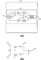
- Figure 1 shows that in some implementations, the present disclosure relates to a 3G/4G front-end architecture 100 that can accommodate one or more 2G amplification paths 104.
- Such an architecture can include a plurality of 3G/4G amplification paths 102 to provide, for example, MMMB functionalities.
- Figure 2 shows an example of a 2G path 104 that can utilize components that are parts of a 3G/4G architecture 100.
- a first path that includes a PA 116 (PA1) and an output matching network 118 (OMN1) is a 3G/4G path.
- a second path that includes a PA 122 (PA2) and an output matching network 124 (OMN2) is a 3G/4G path.
- first and second 3G/4G paths are described in an example context of low band (LB) and very low band (VLB) paths.
- LB low band
- VLB very low band
- the 2G path 104 can include an input 110 configured to receive a 2G signal (e.g., Low Band GSM850 or EGSM900).
- a 2G signal e.g., Low Band GSM850 or EGSM900
- Such a signal can be divided by a splitter 112 into the first path associated with PA1 and the second path associated with PA2.
- the first path is shown to include a phase shifting circuit 114 before PA1, and the output matching network OMN1 after PA1.
- the second path is shown to include the output matching network OMN2 after PA2.
- the two paths are shown to be combined by a Wilkinson combiner 120 so as to yield an output 128 for the amplified 2G signal.
- Figure 3 shows an example of the Wilkinson combiner 120 of Figure 2 .
- First and second nodes 130, 132 can be connected to the outputs of OMN1 and OMN2, respectively, of Figure 2 .
- Such two nodes (130, 132) are shown to be resistively coupled through resistance R1.
- the first node 130 is shown to be coupled to ground through capacitance C1
- the second node 132 is shown to be coupled to ground through capacitance C2.
- Inductances L1 and L2 in series with each other and collectively parallel with R1 are shown to couple the first and second nodes 130, 132, such that the output 128 is at a node between L1 and L2.
- the output node 128 is shown to be coupled to ground through capacitance C3.
- the splitter 112 e.g., one or more switches
- the splitter 112 can be configured so that a given 2G signal is routed to the first path only, to the second path only, or to both of the first and second paths.
- Table 1 lists examples of saturated power level (Psat) performance that can be obtained or expected for the configuration of Figures 2 and 3 (with or without the Wilkinson combiner), when a 2G signal (824 MHz or 915 MHz) is amplified.
- the lossless Wilkinson combiner 120 in Figure 3
- the foregoing design that utilizes a Wilkinson combiner can include at least four SMT components, a resistor having high power rating, and two extra switch arms (e.g., to split the incoming 2G signal).
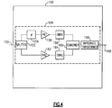
- Figure 4 shows an example of a 2G path 104 that can utilize components that are parts of a 3G/4G architecture 100.
- an additional shared throw can be implemented on an existing post-PA band-select switch to allow two low band 3G/4G amplifiers to be simultaneously connected to a common output pole of the post-PA band-select switch. From such an output pole, an impedance transformation network can be provided to optimally combine the outputs of the two PAs, to thereby reach a larger output power specification typically associated with 2G low bands.
- the post-PA band select switch can effectively isolate the foregoing combiner network from other 3G/4G optimized PAs and related paths; accordingly, there is little or no impact on the performance of various 3G/4G operations.
- a first path that includes a PA 156 (PA1) and an output matching network 158 (OMN1) is a 3G/4G path.
- a second path that includes a PA 162 (PA2) and an output matching network 164 (OMN2) is a 3G/4G path.
- first and second 3G/4G paths are described in an example context of low band (LB) and very low band (VLB) paths.
- LB low band
- VLB very low band
- the 2G path 104 can include an input 150 configured to receive a 2G signal (e.g., Low Band GSM850 or EGSM900).
- a 2G signal e.g., Low Band GSM850 or EGSM900
- Such a signal can be divided by a splitter 152 into the first path associated with PA1 and the second path associated with PA2.
- the first path is shown to include a phase shifting circuit 154 before PA1, and the output matching network OMN1 after PA1.
- the second path is shown to include the output matching network OMN2 after PA2.
- the two paths are shown to be combined by a combiner 160, and the combined path is shown to include an impedance transformer 166 configured to yield an output 168 for the amplified 2G signal.
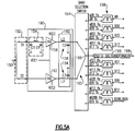
- Figure 5A shows an embodiment of the 3G/4G architecture 100 of Figure 4 .
- the splitter 152, the phase shifting circuit 154, the OMNs 158, 164, and the combiner 160 of Figure 4 are generally indicated with the same reference numbers.
- Figure 5A shows that in some embodiments, the splitter 152 can include first and second switches S1, S2 connected to a common input 150.
- the first switch S1 is shown to be in series with the phase shifting circuit 154 and the first PA 156 (PA1).
- the second switch S2 is shown to be in series with the second PA 162 (PA2).
- operations of the first and second switches S1, S2 can route an incoming 2G signal to the first PA (PA1) only (e.g., S1 closed, S2 open), to the second PA (PA2) only (e.g., S1 open, S2 closed), or to both of the first and second PAs (PA1 and PA2) (e.g., S1 closed, S2 closed).
- S1 and S2 are both closed; accordingly, the incoming 2G signal is routed to both of the first and second PAs (PA1 and PA2).
- the phase shifting circuit 154 can include an inductance L1, with each end of L1 being coupled to ground through a capacitance (C1 or C1').
- Such an example configuration of the phase shifting circuit 154 can provide a phase shift of approximately 60 degrees for the low band 2G signal. It will be understood that the phase shifting circuit 154 can be configured to provide a different amount of phase shift, and/or to accommodate a different frequency signal.
- each of the first and second PAs can include one or more stages.
- each PA can include a driver stage and an output stage.
- each PA in Figure 5A can be provided with a supply voltage VCC1 for the driver stage, and a supply voltage VCC2 for the output stage.
- FIG. 5A shows that in some embodiments, both of the OMNs 158, 164 can be implemented as an integrated passive device (IPD) 192.
- IPD integrated passive device
- Such an IPD can also include matching networks for other 3G/4G PAs.
- Figure 5A shows that in some embodiments, the phase shifting circuit 154, the PAs (PA1, PA2), and the IPD 192 with the OMNs 158, 164 can be considered to be functionally a PA block 190.
- a functional block can be implemented in one or more die.
- the IPD 192 and a die with the PAs can be stacked to reduce lateral footprint size.
- the IPD 192 and a band selection switch 194 of Figure 5A can be stacked. As one can see, a number of different configurations can be implemented.
- Figure 5A shows that in some embodiments, the combiner 160 of Figure 4 can be implemented in the band selection switch 194.
- the outputs of the OMNs 158, 164 for the first and second paths are shown to be connected to their respective poles that may or may not already exist in the band selection switch 194 for 3G/4G operations.
- Various throws in the band selection switch 194 are shown to be connected to their respective duplexers 198.
- An additional throw 196 can be provided in the band selection switch 194, and such a throw can be connected to an impedance transformer 166 as described herein.
- the band selection switch 194 can be operated to form connections between the output of the first OMN 158 and the throw 196, and between the output of the second OMN 164 and the throw 196, to thereby provide a combined path that includes the impedance transformer 166 and the output 168.
- the duplexers 198 are depicted as including channels for example bands B8, B26, B20, B17, B27, B13, B28, B12, and B28B/B29. It will be understood that more or less numbers of bands, and/or other bands, can be implemented and switched through the band selection switch 194.
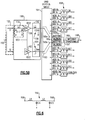
- Figure 5B shows an alternate design for the example of Figure 5A . More particularly, the example of Figure 5B is shown to include a combiner 160 that is different than the combiner of Figure 5A .
- the splitter 152, the PA block 190, and the duplexers 198 of Figure 5B can be similar to those of Figure 5A .
- the outputs of the OMNs 158, 164 for the first and second paths are shown to be connected to their respective poles that may or may not already exist in the band selection switch 194 for 3G/4G operations, similar to the embodiment of Figure 5A .
- the band selection switch 194 of Figure 5B there are two throws 193a, 193b that can be connected to such two poles.
- the throw 193a is shown to be connected to an input of a first matching network 195a
- the throw 193b is shown to be connected to an input of a second matching network 195b.
- Outputs of the first and second matching networks 195a, 195b are shown to be connected to a common node 197.
- the combiner in the example of Figure 5B can include the foregoing paths between the OMNs 158, 164 and the common node 197.
- an impedance transformer 166 is shown to be implemented between the common node 197 and the output 168.
- Such an impedance transformer may or may not be the same as the example 25ohm-to-50ohm transformer of Figure 5A .
- FIG 6 shows an example circuit that can be implemented as the impedance transformer 166 of Figures 5A and 5B .
- Such a circuit can include inductances L4 and L5 connected in series between the common throw 196 of the band selection switch 194 and the output 168 of Figure 5A , and between the common node 197 and the output 168 of Figure 5B .
- the impedance transformer circuit 166 is shown to further include capacitance C4 that couples a node between L4 and L5 to ground, and capacitance C5 that couples the output node 128 to ground.
- the impedance transformer 166 is depicted as providing 25 ohm (on the common node (196) side) to 50 ohm (on the output (168) side) transformation.
- values of L4, L5, C4 and C5 in Figure 6 can be as follows.
- L4 can be approximately 3.74 nH
- L5 can be approximately 7.91 nH
- C4 can be approximately 6.33 pF
- C5 can be approximately 2.99 pF.
- L4 can be approximately 3.6 nH
- L5 can be approximately 7.7 nH
- C4 can be approximately 6.2 pF
- C5 can be approximately 3 pF.
- Such an example configuration of the impedance transformer 166 can enhance output power for the low band 2G signal processed as described herein. It will be understood that the impedance transformer 166 can be configured to provide different transformations, and/or to accommodate a different frequency signals.
- the impedance transformer 166 of Figures 4-6 may be implemented using a number of other techniques, including, for example, transmission lines, lumped element reactive transformation, and transformer based on coupled coils of various winding relationships to achieve different impedance transformations.
- Required or desired phase and amplitude relationships between the two PA paths can be achieved through, for example, application of phase shifting and amplitude adjustment at the input of one or the other, or combinations of the stages relative to the other in order to avoid output losses.
- the phase and amplitude adjustment networks can also be implemented at the output side of PA(s), with some loss penalty.
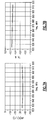
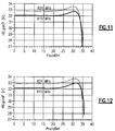
- Figure 7A shows a plot of S11 parameter (reflection coefficient) as a function of frequency, demonstrating broadband property.
- Figure 7B shows a plot of insertion loss as a function of frequency, demonstrating a reasonable insertion loss of about 0.3 dB.
- the load-sharing configuration of Figure 5A provides good performance similar to the level of performance provided by the lossless Wilkinson-combiner example of Figure 2 .
- the load-sharing configuration of Figure 5A can be implemented with much less number of extra components. Accordingly, the load-sharing configuration of Figure 5A can provide advantageous savings in cost and space.
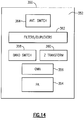
- FIG 14 shows that in some embodiments, some of all of the 3G/4G architecture as described herein can be implemented as a packaged module.
- a front-end module (FEM) 350 can include a packaging substrate 352 configured to receive a plurality of components.
- Such components include, for example, a PA die 354 having a plurality of amplification paths to facilitate 3G/4G MMMB operations.
- a PA die 354 having a plurality of amplification paths to facilitate 3G/4G MMMB operations.
- 2G PAs are traditionally implemented on such a die
- some or all of such 2G PAs can be eliminated, and 2G functionalities can be achieved, by utilizing one or more of the techniques described herein. Accordingly, such a PA die size and cost can be reduced.
- the example FEM 350 is shown to further include an assembly of filters and duplexers 362.
- filters and duplexers can provide filtering and duplexing functionalities for 3G/4G signals, as well as 2G signals processed through the 3G/4G engine.
- a wireless device does not need to be a multi-band device.
- a wireless device can include additional antennas such as diversity antenna, and additional connectivity features such as Wi-Fi, Bluetooth, and GPS.
Landscapes
- Engineering & Computer Science (AREA)
- Power Engineering (AREA)
- Computer Networks & Wireless Communication (AREA)
- Signal Processing (AREA)
- Microelectronics & Electronic Packaging (AREA)
- Amplifiers (AREA)
- Transceivers (AREA)
- Transmitters (AREA)
Applications Claiming Priority (2)
| Application Number | Priority Date | Filing Date | Title |
|---|---|---|---|
| US201462038322P | 2014-08-17 | 2014-08-17 | |
| US201462038323P | 2014-08-17 | 2014-08-17 |
Publications (2)
| Publication Number | Publication Date |
|---|---|
| EP2988416A1 EP2988416A1 (en) | 2016-02-24 |
| EP2988416B1 true EP2988416B1 (en) | 2019-11-06 |
Family
ID=53871959
Family Applications (2)
| Application Number | Title | Priority Date | Filing Date |
|---|---|---|---|
| EP15181220.3A Active EP2988416B1 (en) | 2014-08-17 | 2015-08-17 | Circuits and methods for 2g amplification using 3g/4g linear path combination |
| EP15181239.3A Active EP2988417B1 (en) | 2014-08-17 | 2015-08-17 | Power amplifier interface compatible with inputs separated by mode or frequency |
Family Applications After (1)
| Application Number | Title | Priority Date | Filing Date |
|---|---|---|---|
| EP15181239.3A Active EP2988417B1 (en) | 2014-08-17 | 2015-08-17 | Power amplifier interface compatible with inputs separated by mode or frequency |
Country Status (5)
| Country | Link |
|---|---|
| US (3) | US10153736B2 (enExample) |
| EP (2) | EP2988416B1 (enExample) |
| JP (4) | JP6498563B2 (enExample) |
| CN (3) | CN111585534B (enExample) |
| TW (2) | TWI672918B (enExample) |
Families Citing this family (38)
| Publication number | Priority date | Publication date | Assignee | Title |
|---|---|---|---|---|
| JP6616241B2 (ja) * | 2015-05-22 | 2019-12-04 | スカイワークス ソリューションズ,インコーポレイテッド | 電力増幅器用の並列機能を有する出力整合ネットワーク及びフィルタの結合体 |
| CN107925536B (zh) * | 2015-07-06 | 2021-10-29 | 瑞典爱立信有限公司 | 用于无线系统中数据传送的资源分配 |
| JP2017103655A (ja) * | 2015-12-02 | 2017-06-08 | 株式会社村田製作所 | 電力増幅モジュール |
| KR102468952B1 (ko) * | 2016-03-07 | 2022-11-22 | 삼성전자주식회사 | 신호를 송수신하는 전자 장치 및 방법 |
| US9887673B2 (en) * | 2016-03-11 | 2018-02-06 | Intel Corporation | Ultra compact multi-band transmitter with robust AM-PM distortion self-suppression techniques |
| TWI729112B (zh) * | 2016-04-09 | 2021-06-01 | 美商天工方案公司 | 具有可切換雙工器的前端架構 |
| US9948350B2 (en) * | 2016-07-06 | 2018-04-17 | Qorvo Us, Inc. | Multi-mode radio frequency circuitry |
| JP2018050167A (ja) | 2016-09-21 | 2018-03-29 | 株式会社村田製作所 | 電力増幅モジュール |
| US10211784B2 (en) * | 2016-11-03 | 2019-02-19 | Nxp Usa, Inc. | Amplifier architecture reconfiguration |
| US10469033B2 (en) | 2016-11-21 | 2019-11-05 | Murata Manufacturing Co., Ltd. | Power amplification module |
| JP2018085560A (ja) | 2016-11-21 | 2018-05-31 | 株式会社村田製作所 | 電力増幅モジュール |
| JP2018098766A (ja) | 2016-12-09 | 2018-06-21 | 株式会社村田製作所 | バイアス回路 |
| US10148226B2 (en) | 2016-12-09 | 2018-12-04 | Murata Manufacturing Co., Ltd. | Bias circuit |
| EP3442120B1 (en) * | 2017-08-08 | 2021-02-03 | Rohde & Schwarz GmbH & Co. KG | Amplifier circuit and method |
| JP2019193115A (ja) | 2018-04-25 | 2019-10-31 | 株式会社村田製作所 | 高周波増幅回路、高周波フロントエンド回路および通信装置 |
| CN108768434B (zh) * | 2018-06-06 | 2021-02-12 | 维沃移动通信有限公司 | 一种射频电路、终端及信号发射控制方法 |
| WO2019244757A1 (ja) | 2018-06-19 | 2019-12-26 | 株式会社村田製作所 | 高周波増幅回路および通信装置 |
| US10498298B1 (en) | 2018-08-10 | 2019-12-03 | Qualcomm Incorporated | Time-division duplexing using dynamic transceiver isolation |
| CN109195118A (zh) * | 2018-10-19 | 2019-01-11 | 江苏未来智慧信息科技有限公司 | 基于蓝牙的带pa单向广播通信装置及通信方法 |
| KR102581317B1 (ko) * | 2018-12-24 | 2023-09-22 | 삼성전자 주식회사 | 복수개의 안테나 어레이를 포함하는 전자 장치 |
| JP2020156026A (ja) * | 2019-03-22 | 2020-09-24 | 日本電波工業株式会社 | ログアンプ回路 |
| US11544211B2 (en) * | 2019-04-19 | 2023-01-03 | Parallel Wireless, Inc. | VRAN with PCIe fronthaul |
| KR102658531B1 (ko) * | 2019-05-15 | 2024-04-18 | 삼성전자주식회사 | 단일 안테나를 이용한 다중 대역 통신을 위한 방법 및 그 전자 장치 |
| US11469725B2 (en) | 2019-06-07 | 2022-10-11 | Skyworks Solutions, Inc. | Apparatus and methods for power amplifier output matching |
| US11463116B2 (en) * | 2019-09-20 | 2022-10-04 | Murata Manufacturing Co., Ltd. | Radio frequency module and communication device |
| KR102887576B1 (ko) * | 2020-01-23 | 2025-11-26 | 삼성전자 주식회사 | 무선 신호를 처리하기 위한 전자 장치 및 그의 동작 방법 |
| GB2597359A (en) * | 2020-06-29 | 2022-01-26 | Skyworks Solutions Inc | Dual connectivity power amplifier system |
| JP2022019088A (ja) | 2020-07-17 | 2022-01-27 | 株式会社村田製作所 | 電力増幅モジュール |
| DE112021002738T5 (de) * | 2020-08-13 | 2023-03-02 | Murata Manufacturing Co., Ltd. | Hochfrequenzmodul |
| US12081179B2 (en) | 2020-08-26 | 2024-09-03 | Skyworks Solutions, Inc. | Power management of power amplifier modules |
| GB2603998B (en) | 2020-12-07 | 2023-04-26 | Skyworks Solutions Inc | Radio frequency front end module including common filter |
| CN116746061B (zh) * | 2020-12-28 | 2025-09-05 | 株式会社村田制作所 | 高频电路和通信装置 |
| CN113225092B (zh) * | 2021-04-14 | 2022-11-08 | 荣耀终端有限公司 | 射频放大电路和方法 |
| CN113659997B (zh) * | 2021-08-16 | 2022-12-27 | 荣耀终端有限公司 | 射频放大电路、相位调节方法、射频放大方法和终端设备 |
| US12470201B2 (en) | 2021-08-27 | 2025-11-11 | Skyworks Solutions, Inc. | Packaged multilayer piezoelectric surface acoustic wave device with conductive pillar |
| CN115882791B (zh) * | 2022-12-12 | 2025-08-01 | 深圳飞骧科技股份有限公司 | 一种电压合成式Doherty功率放大器 |
| CN119543848A (zh) * | 2025-01-22 | 2025-02-28 | 上海凡麒微电子有限公司 | 一种多频放大装置 |
| CN120149776B (zh) * | 2025-05-16 | 2025-08-12 | 深圳飞骧科技股份有限公司 | 射频功分单元、射频功分模组及射频接收系统 |
Family Cites Families (44)
| Publication number | Priority date | Publication date | Assignee | Title |
|---|---|---|---|---|
| JP2826433B2 (ja) * | 1993-02-26 | 1998-11-18 | 日本電気株式会社 | アンテナ用二周波整合回路 |
| JP3332194B2 (ja) * | 1995-08-10 | 2002-10-07 | ソニー株式会社 | スイツチ半導体集積回路及び通信端末装置 |
| US5973557A (en) * | 1996-10-18 | 1999-10-26 | Matsushita Electric Industrial Co., Ltd. | High efficiency linear power amplifier of plural frequency bands and high efficiency power amplifier |
| US6091966A (en) * | 1997-09-29 | 2000-07-18 | Ericsson, Inc. | Dual-band, dual-mode power amplifier |
| US6188877B1 (en) * | 1997-07-03 | 2001-02-13 | Ericsson Inc. | Dual-band, dual-mode power amplifier with reduced power loss |
| US7212788B2 (en) * | 2002-08-13 | 2007-05-01 | Atheros Communications, Inc. | Method and apparatus for signal power loss reduction in RF communication systems |
| DE602005000437T2 (de) * | 2004-07-08 | 2007-10-31 | Sony United Kingdom Ltd., Weybridge | Leistungsregelung für Leistungsverstärker |
| JP2007019939A (ja) * | 2005-07-08 | 2007-01-25 | Renesas Technology Corp | 無線通信装置及びそれを用いた携帯電話端末 |
| US7486134B2 (en) * | 2006-03-09 | 2009-02-03 | Skyworks Solutions, Inc. | High efficiency load insensitive power amplifier |
| DE102007019082B4 (de) * | 2007-04-23 | 2018-04-05 | Snaptrack Inc. | Frontendmodul |
| TWI346449B (en) * | 2007-08-16 | 2011-08-01 | Ind Tech Res Inst | Power amplifier circuit for multi-frequencies and multi-modes and method for operating the same |
| DE102007050606B3 (de) * | 2007-10-23 | 2009-04-23 | Epcos Ag | Schaltungsanordnung für eine Mobilfunkeinrichtung und Verfahren zum Betrieb |
| US7853290B2 (en) * | 2007-10-29 | 2010-12-14 | Infineon Technologies Ag | Transmitter arrangement |
| US7876160B2 (en) * | 2008-02-04 | 2011-01-25 | Skyworks Solutions, Inc. | Multi-mode high efficiency linear power amplifier |
| US8095092B2 (en) * | 2008-06-26 | 2012-01-10 | Infineon Technologies Ag | Power efficient transmitter with high dynamic range |
| US7619468B1 (en) * | 2008-09-30 | 2009-11-17 | Nortel Networks Limited | Doherty amplifier with drain bias supply modulation |
| US8447255B2 (en) * | 2008-10-28 | 2013-05-21 | Sony Ericsson Mobile Communications Ab | Variable impedance matching network and method for the same |
| US8457685B1 (en) * | 2009-04-20 | 2013-06-04 | Rf Micro Devices, Inc. | Method and system for increasing efficiency in a radio front-end |
| JP2010273321A (ja) * | 2009-04-22 | 2010-12-02 | Panasonic Corp | 高周波電力増幅装置及びそれを有する無線通信装置 |
| US8467738B2 (en) * | 2009-05-04 | 2013-06-18 | Rfaxis, Inc. | Multi-mode radio frequency front end module |
| US8971830B2 (en) * | 2009-05-12 | 2015-03-03 | Qualcomm Incorporated | Multi-mode multi-band power amplifier module |
| US8195119B2 (en) * | 2009-05-13 | 2012-06-05 | Qualcomm, Incorporated | Switchable input pair operational amplifiers |
| US8750810B2 (en) * | 2009-07-24 | 2014-06-10 | Qualcomm Incorporated | Power amplifier with switched output matching for multi-mode operation |
| JP5370097B2 (ja) | 2009-11-24 | 2013-12-18 | 富士通株式会社 | 通信端末装置、通信回路及び通信方法 |
| US8912847B2 (en) | 2009-12-03 | 2014-12-16 | Epcos Ag | Power amplifier circuit and front end circuit |
| US8849272B2 (en) * | 2010-02-25 | 2014-09-30 | Mediatek Inc. | Methods for coordinating radio activities in different radio access technologies and apparatuses utilizing the same |
| US20120202561A1 (en) * | 2011-02-07 | 2012-08-09 | Qualcomm Incorporated | Cdma transceiver with cdma diversity receiver path shared with time duplexed receiver |
| WO2013027538A1 (ja) * | 2011-08-23 | 2013-02-28 | 日本電気株式会社 | 送信機 |
| US9679869B2 (en) * | 2011-09-02 | 2017-06-13 | Skyworks Solutions, Inc. | Transmission line for high performance radio frequency applications |
| DE112011105649T5 (de) | 2011-09-22 | 2014-08-28 | Epcos Ag | Eingangsschaltung für Bandaggregationsbetriebsarten |
| US8634782B2 (en) * | 2011-10-14 | 2014-01-21 | Qualcomm Incorporated | Multi-antenna wireless device with power combining power amplifiers |
| CN102404879B (zh) * | 2011-11-04 | 2016-04-13 | 惠州Tcl移动通信有限公司 | 一种移动通讯终端 |
| US9143125B2 (en) * | 2011-11-09 | 2015-09-22 | Skyworks Solutions, Inc. | Radio-frequency switches having extended termination bandwidth and related circuits, modules, methods, and systems |
| CN103178791A (zh) * | 2011-12-26 | 2013-06-26 | 深圳富泰宏精密工业有限公司 | 功率放大电路及具有该功率放大电路的无线通信装置 |
| KR101763997B1 (ko) * | 2012-04-12 | 2017-08-01 | 스카이워크스 솔루션즈, 인코포레이티드 | 전송 무선 주파수 신호와 수신 무선 주파수 신호 간의 개선된 격리에 관한 시스템 및 방법 |
| US8987851B2 (en) * | 2012-09-07 | 2015-03-24 | Mediatek Inc. | Radio-frequency device package and method for fabricating the same |
| CN202889657U (zh) * | 2012-10-25 | 2013-04-17 | 宏达国际电子股份有限公司 | 双模双待双通的移动通讯装置 |
| US9130600B2 (en) * | 2012-12-18 | 2015-09-08 | Broadcom Corporation | Receiver architecture with reconfigurable on-chip matching for wideband operation and off-chip matching for low-power operation |
| US9337991B2 (en) * | 2013-04-19 | 2016-05-10 | Mediatek Singapore Pte. Ltd. | Wireless communication unit, radio frequency module and method therefor |
| US9065541B2 (en) * | 2013-09-10 | 2015-06-23 | Broadcom Corporation | Configurable wireless communication device with configurable front-end |
| US9276552B2 (en) * | 2013-09-26 | 2016-03-01 | Rf Micro Devices, Inc. | Output match directional coupler |
| CN106464218B (zh) * | 2014-02-25 | 2019-05-10 | 天工方案公司 | 关于改进的射频模块的系统、设备和方法 |
| JP2015160631A (ja) | 2014-02-27 | 2015-09-07 | 凸版印刷株式会社 | 電子レンジ加熱用包装容器 |
| EP3164943A2 (en) * | 2014-07-01 | 2017-05-10 | Sofant Technologies Ltd | Wireless communications apparatus |
-
2015
- 2015-08-17 TW TW104126768A patent/TWI672918B/zh active
- 2015-08-17 EP EP15181220.3A patent/EP2988416B1/en active Active
- 2015-08-17 CN CN202010458421.4A patent/CN111585534B/zh active Active
- 2015-08-17 US US14/827,534 patent/US10153736B2/en active Active
- 2015-08-17 CN CN201510504543.1A patent/CN105376660B/zh active Active
- 2015-08-17 JP JP2015160631A patent/JP6498563B2/ja active Active
- 2015-08-17 TW TW104126769A patent/TWI711270B/zh active
- 2015-08-17 CN CN201510505346.1A patent/CN105375968B/zh active Active
- 2015-08-17 US US14/827,543 patent/US20160190995A1/en not_active Abandoned
- 2015-08-17 JP JP2015160637A patent/JP2016042700A/ja active Pending
- 2015-08-17 EP EP15181239.3A patent/EP2988417B1/en active Active
-
2018
- 2018-12-04 US US16/208,873 patent/US11323073B2/en active Active
-
2019
- 2019-03-13 JP JP2019046251A patent/JP6890146B6/ja active Active
-
2021
- 2021-06-15 JP JP2021099599A patent/JP2021153326A/ja active Pending
Non-Patent Citations (1)
| Title |
|---|
| None * |
Also Published As
| Publication number | Publication date |
|---|---|
| JP2016042699A (ja) | 2016-03-31 |
| EP2988417A1 (en) | 2016-02-24 |
| EP2988417B1 (en) | 2020-05-13 |
| CN105375968A (zh) | 2016-03-02 |
| CN105376660B (zh) | 2020-10-30 |
| US10153736B2 (en) | 2018-12-11 |
| JP2019134460A (ja) | 2019-08-08 |
| US20160190995A1 (en) | 2016-06-30 |
| CN111585534B (zh) | 2024-03-19 |
| TW201613286A (en) | 2016-04-01 |
| TWI672918B (zh) | 2019-09-21 |
| CN105376660A (zh) | 2016-03-02 |
| JP6890146B6 (ja) | 2021-07-14 |
| CN105375968B (zh) | 2020-05-22 |
| JP2016042700A (ja) | 2016-03-31 |
| US20190386616A1 (en) | 2019-12-19 |
| CN111585534A (zh) | 2020-08-25 |
| HK1216468A1 (zh) | 2016-11-11 |
| TW201620245A (zh) | 2016-06-01 |
| JP6890146B2 (ja) | 2021-06-18 |
| US20160191105A1 (en) | 2016-06-30 |
| JP6498563B2 (ja) | 2019-04-10 |
| JP2021153326A (ja) | 2021-09-30 |
| US11323073B2 (en) | 2022-05-03 |
| TWI711270B (zh) | 2020-11-21 |
| EP2988416A1 (en) | 2016-02-24 |
| HK1216471A1 (zh) | 2016-11-11 |
Similar Documents
| Publication | Publication Date | Title |
|---|---|---|
| EP2988416B1 (en) | Circuits and methods for 2g amplification using 3g/4g linear path combination | |
| US11764734B2 (en) | Signal combiner having a tuned termination circuit on an isolation port for a Doherty power amplifier | |
| US10778152B2 (en) | Methods for amplifying signals using a Doherty amplifier | |
| CN108011600B (zh) | 一种可重构的射频及微波功率放大器 | |
| KR102483467B1 (ko) | 선형의 효율적인 광대역 전력 증폭기들에 관한 시스템들 및 방법들 | |
| US9912299B2 (en) | Architectures and devices related to Doherty amplifiers | |
| TWI641214B (zh) | 功率放大系統、射頻模組、無線裝置及用於處理射頻信號之方法 | |
| KR102603312B1 (ko) | 감소된 크기를 갖는 도허티 전력 증폭기 | |
| CN105375883B (zh) | 具有可调阻抗终端电路的多尔蒂功率放大器组合器 | |
| HK40036785A (en) | Circuits and methods for 2g amplification using 3g/4g linear path combination | |
| HK1216468B (zh) | 進行2g放大的電路、方法和無線裝置 | |
| HK40036785B (zh) | 使用3g/4g线性路径组合进行2g放大的电路和方法 |
Legal Events
| Date | Code | Title | Description |
|---|---|---|---|
| PUAI | Public reference made under article 153(3) epc to a published international application that has entered the european phase |
Free format text: ORIGINAL CODE: 0009012 |
|
| AK | Designated contracting states |
Kind code of ref document: A1 Designated state(s): AL AT BE BG CH CY CZ DE DK EE ES FI FR GB GR HR HU IE IS IT LI LT LU LV MC MK MT NL NO PL PT RO RS SE SI SK SM TR |
|
| AX | Request for extension of the european patent |
Extension state: BA ME |
|
| 17P | Request for examination filed |
Effective date: 20160819 |
|
| RBV | Designated contracting states (corrected) |
Designated state(s): AL AT BE BG CH CY CZ DE DK EE ES FI FR GB GR HR HU IE IS IT LI LT LU LV MC MK MT NL NO PL PT RO RS SE SI SK SM TR |
|
| STAA | Information on the status of an ep patent application or granted ep patent |
Free format text: STATUS: EXAMINATION IS IN PROGRESS |
|
| 17Q | First examination report despatched |
Effective date: 20180917 |
|
| GRAP | Despatch of communication of intention to grant a patent |
Free format text: ORIGINAL CODE: EPIDOSNIGR1 |
|
| STAA | Information on the status of an ep patent application or granted ep patent |
Free format text: STATUS: GRANT OF PATENT IS INTENDED |
|
| INTG | Intention to grant announced |
Effective date: 20190710 |
|
| GRAS | Grant fee paid |
Free format text: ORIGINAL CODE: EPIDOSNIGR3 |
|
| GRAA | (expected) grant |
Free format text: ORIGINAL CODE: 0009210 |
|
| STAA | Information on the status of an ep patent application or granted ep patent |
Free format text: STATUS: THE PATENT HAS BEEN GRANTED |
|
| AK | Designated contracting states |
Kind code of ref document: B1 Designated state(s): AL AT BE BG CH CY CZ DE DK EE ES FI FR GB GR HR HU IE IS IT LI LT LU LV MC MK MT NL NO PL PT RO RS SE SI SK SM TR |
|
| REG | Reference to a national code |
Ref country code: GB Ref legal event code: FG4D |
|
| REG | Reference to a national code |
Ref country code: CH Ref legal event code: EP Ref country code: AT Ref legal event code: REF Ref document number: 1200175 Country of ref document: AT Kind code of ref document: T Effective date: 20191115 |
|
| REG | Reference to a national code |
Ref country code: IE Ref legal event code: FG4D |
|
| REG | Reference to a national code |
Ref country code: DE Ref legal event code: R096 Ref document number: 602015040986 Country of ref document: DE |
|
| REG | Reference to a national code |
Ref country code: NL Ref legal event code: MP Effective date: 20191106 |
|
| REG | Reference to a national code |
Ref country code: LT Ref legal event code: MG4D |
|
| PG25 | Lapsed in a contracting state [announced via postgrant information from national office to epo] |
Ref country code: NL Free format text: LAPSE BECAUSE OF FAILURE TO SUBMIT A TRANSLATION OF THE DESCRIPTION OR TO PAY THE FEE WITHIN THE PRESCRIBED TIME-LIMIT Effective date: 20191106 Ref country code: SE Free format text: LAPSE BECAUSE OF FAILURE TO SUBMIT A TRANSLATION OF THE DESCRIPTION OR TO PAY THE FEE WITHIN THE PRESCRIBED TIME-LIMIT Effective date: 20191106 Ref country code: LV Free format text: LAPSE BECAUSE OF FAILURE TO SUBMIT A TRANSLATION OF THE DESCRIPTION OR TO PAY THE FEE WITHIN THE PRESCRIBED TIME-LIMIT Effective date: 20191106 Ref country code: PL Free format text: LAPSE BECAUSE OF FAILURE TO SUBMIT A TRANSLATION OF THE DESCRIPTION OR TO PAY THE FEE WITHIN THE PRESCRIBED TIME-LIMIT Effective date: 20191106 Ref country code: NO Free format text: LAPSE BECAUSE OF FAILURE TO SUBMIT A TRANSLATION OF THE DESCRIPTION OR TO PAY THE FEE WITHIN THE PRESCRIBED TIME-LIMIT Effective date: 20200206 Ref country code: PT Free format text: LAPSE BECAUSE OF FAILURE TO SUBMIT A TRANSLATION OF THE DESCRIPTION OR TO PAY THE FEE WITHIN THE PRESCRIBED TIME-LIMIT Effective date: 20200306 Ref country code: BG Free format text: LAPSE BECAUSE OF FAILURE TO SUBMIT A TRANSLATION OF THE DESCRIPTION OR TO PAY THE FEE WITHIN THE PRESCRIBED TIME-LIMIT Effective date: 20200206 Ref country code: FI Free format text: LAPSE BECAUSE OF FAILURE TO SUBMIT A TRANSLATION OF THE DESCRIPTION OR TO PAY THE FEE WITHIN THE PRESCRIBED TIME-LIMIT Effective date: 20191106 Ref country code: GR Free format text: LAPSE BECAUSE OF FAILURE TO SUBMIT A TRANSLATION OF THE DESCRIPTION OR TO PAY THE FEE WITHIN THE PRESCRIBED TIME-LIMIT Effective date: 20200207 Ref country code: LT Free format text: LAPSE BECAUSE OF FAILURE TO SUBMIT A TRANSLATION OF THE DESCRIPTION OR TO PAY THE FEE WITHIN THE PRESCRIBED TIME-LIMIT Effective date: 20191106 |
|
| PG25 | Lapsed in a contracting state [announced via postgrant information from national office to epo] |
Ref country code: HR Free format text: LAPSE BECAUSE OF FAILURE TO SUBMIT A TRANSLATION OF THE DESCRIPTION OR TO PAY THE FEE WITHIN THE PRESCRIBED TIME-LIMIT Effective date: 20191106 Ref country code: IS Free format text: LAPSE BECAUSE OF FAILURE TO SUBMIT A TRANSLATION OF THE DESCRIPTION OR TO PAY THE FEE WITHIN THE PRESCRIBED TIME-LIMIT Effective date: 20200306 Ref country code: RS Free format text: LAPSE BECAUSE OF FAILURE TO SUBMIT A TRANSLATION OF THE DESCRIPTION OR TO PAY THE FEE WITHIN THE PRESCRIBED TIME-LIMIT Effective date: 20191106 |
|
| PG25 | Lapsed in a contracting state [announced via postgrant information from national office to epo] |
Ref country code: AL Free format text: LAPSE BECAUSE OF FAILURE TO SUBMIT A TRANSLATION OF THE DESCRIPTION OR TO PAY THE FEE WITHIN THE PRESCRIBED TIME-LIMIT Effective date: 20191106 |
|
| PG25 | Lapsed in a contracting state [announced via postgrant information from national office to epo] |
Ref country code: CZ Free format text: LAPSE BECAUSE OF FAILURE TO SUBMIT A TRANSLATION OF THE DESCRIPTION OR TO PAY THE FEE WITHIN THE PRESCRIBED TIME-LIMIT Effective date: 20191106 Ref country code: ES Free format text: LAPSE BECAUSE OF FAILURE TO SUBMIT A TRANSLATION OF THE DESCRIPTION OR TO PAY THE FEE WITHIN THE PRESCRIBED TIME-LIMIT Effective date: 20191106 Ref country code: RO Free format text: LAPSE BECAUSE OF FAILURE TO SUBMIT A TRANSLATION OF THE DESCRIPTION OR TO PAY THE FEE WITHIN THE PRESCRIBED TIME-LIMIT Effective date: 20191106 Ref country code: EE Free format text: LAPSE BECAUSE OF FAILURE TO SUBMIT A TRANSLATION OF THE DESCRIPTION OR TO PAY THE FEE WITHIN THE PRESCRIBED TIME-LIMIT Effective date: 20191106 Ref country code: DK Free format text: LAPSE BECAUSE OF FAILURE TO SUBMIT A TRANSLATION OF THE DESCRIPTION OR TO PAY THE FEE WITHIN THE PRESCRIBED TIME-LIMIT Effective date: 20191106 |
|
| REG | Reference to a national code |
Ref country code: DE Ref legal event code: R097 Ref document number: 602015040986 Country of ref document: DE |
|
| REG | Reference to a national code |
Ref country code: AT Ref legal event code: MK05 Ref document number: 1200175 Country of ref document: AT Kind code of ref document: T Effective date: 20191106 |
|
| PG25 | Lapsed in a contracting state [announced via postgrant information from national office to epo] |
Ref country code: SM Free format text: LAPSE BECAUSE OF FAILURE TO SUBMIT A TRANSLATION OF THE DESCRIPTION OR TO PAY THE FEE WITHIN THE PRESCRIBED TIME-LIMIT Effective date: 20191106 Ref country code: SK Free format text: LAPSE BECAUSE OF FAILURE TO SUBMIT A TRANSLATION OF THE DESCRIPTION OR TO PAY THE FEE WITHIN THE PRESCRIBED TIME-LIMIT Effective date: 20191106 |
|
| PLBE | No opposition filed within time limit |
Free format text: ORIGINAL CODE: 0009261 |
|
| STAA | Information on the status of an ep patent application or granted ep patent |
Free format text: STATUS: NO OPPOSITION FILED WITHIN TIME LIMIT |
|
| 26N | No opposition filed |
Effective date: 20200807 |
|
| PG25 | Lapsed in a contracting state [announced via postgrant information from national office to epo] |
Ref country code: AT Free format text: LAPSE BECAUSE OF FAILURE TO SUBMIT A TRANSLATION OF THE DESCRIPTION OR TO PAY THE FEE WITHIN THE PRESCRIBED TIME-LIMIT Effective date: 20191106 Ref country code: SI Free format text: LAPSE BECAUSE OF FAILURE TO SUBMIT A TRANSLATION OF THE DESCRIPTION OR TO PAY THE FEE WITHIN THE PRESCRIBED TIME-LIMIT Effective date: 20191106 |
|
| PG25 | Lapsed in a contracting state [announced via postgrant information from national office to epo] |
Ref country code: IT Free format text: LAPSE BECAUSE OF FAILURE TO SUBMIT A TRANSLATION OF THE DESCRIPTION OR TO PAY THE FEE WITHIN THE PRESCRIBED TIME-LIMIT Effective date: 20191106 |
|
| PG25 | Lapsed in a contracting state [announced via postgrant information from national office to epo] |
Ref country code: MC Free format text: LAPSE BECAUSE OF FAILURE TO SUBMIT A TRANSLATION OF THE DESCRIPTION OR TO PAY THE FEE WITHIN THE PRESCRIBED TIME-LIMIT Effective date: 20191106 |
|
| REG | Reference to a national code |
Ref country code: CH Ref legal event code: PL |
|
| PG25 | Lapsed in a contracting state [announced via postgrant information from national office to epo] |
Ref country code: CH Free format text: LAPSE BECAUSE OF NON-PAYMENT OF DUE FEES Effective date: 20200831 Ref country code: LU Free format text: LAPSE BECAUSE OF NON-PAYMENT OF DUE FEES Effective date: 20200817 Ref country code: LI Free format text: LAPSE BECAUSE OF NON-PAYMENT OF DUE FEES Effective date: 20200831 |
|
| REG | Reference to a national code |
Ref country code: BE Ref legal event code: MM Effective date: 20200831 |
|
| PG25 | Lapsed in a contracting state [announced via postgrant information from national office to epo] |
Ref country code: IE Free format text: LAPSE BECAUSE OF NON-PAYMENT OF DUE FEES Effective date: 20200817 Ref country code: BE Free format text: LAPSE BECAUSE OF NON-PAYMENT OF DUE FEES Effective date: 20200831 |
|
| PG25 | Lapsed in a contracting state [announced via postgrant information from national office to epo] |
Ref country code: TR Free format text: LAPSE BECAUSE OF FAILURE TO SUBMIT A TRANSLATION OF THE DESCRIPTION OR TO PAY THE FEE WITHIN THE PRESCRIBED TIME-LIMIT Effective date: 20191106 Ref country code: MT Free format text: LAPSE BECAUSE OF FAILURE TO SUBMIT A TRANSLATION OF THE DESCRIPTION OR TO PAY THE FEE WITHIN THE PRESCRIBED TIME-LIMIT Effective date: 20191106 Ref country code: CY Free format text: LAPSE BECAUSE OF FAILURE TO SUBMIT A TRANSLATION OF THE DESCRIPTION OR TO PAY THE FEE WITHIN THE PRESCRIBED TIME-LIMIT Effective date: 20191106 |
|
| PG25 | Lapsed in a contracting state [announced via postgrant information from national office to epo] |
Ref country code: MK Free format text: LAPSE BECAUSE OF FAILURE TO SUBMIT A TRANSLATION OF THE DESCRIPTION OR TO PAY THE FEE WITHIN THE PRESCRIBED TIME-LIMIT Effective date: 20191106 |
|
| PGFP | Annual fee paid to national office [announced via postgrant information from national office to epo] |
Ref country code: DE Payment date: 20250827 Year of fee payment: 11 |
|
| PGFP | Annual fee paid to national office [announced via postgrant information from national office to epo] |
Ref country code: GB Payment date: 20250827 Year of fee payment: 11 |
|
| PGFP | Annual fee paid to national office [announced via postgrant information from national office to epo] |
Ref country code: FR Payment date: 20250825 Year of fee payment: 11 |