EP2988407A2 - Control method and control system of three level inverter - Google Patents
Control method and control system of three level inverter Download PDFInfo
- Publication number
- EP2988407A2 EP2988407A2 EP15180324.4A EP15180324A EP2988407A2 EP 2988407 A2 EP2988407 A2 EP 2988407A2 EP 15180324 A EP15180324 A EP 15180324A EP 2988407 A2 EP2988407 A2 EP 2988407A2
- Authority
- EP
- European Patent Office
- Prior art keywords
- value
- voltage
- phase
- voltage command
- output
- Prior art date
- Legal status (The legal status is an assumption and is not a legal conclusion. Google has not performed a legal analysis and makes no representation as to the accuracy of the status listed.)
- Granted
Links
Images







Classifications
-
- H—ELECTRICITY
- H02—GENERATION; CONVERSION OR DISTRIBUTION OF ELECTRIC POWER
- H02M—APPARATUS FOR CONVERSION BETWEEN AC AND AC, BETWEEN AC AND DC, OR BETWEEN DC AND DC, AND FOR USE WITH MAINS OR SIMILAR POWER SUPPLY SYSTEMS; CONVERSION OF DC OR AC INPUT POWER INTO SURGE OUTPUT POWER; CONTROL OR REGULATION THEREOF
- H02M7/00—Conversion of AC power input into DC power output; Conversion of DC power input into AC power output
- H02M7/42—Conversion of DC power input into AC power output without possibility of reversal
- H02M7/44—Conversion of DC power input into AC power output without possibility of reversal by static converters
- H02M7/48—Conversion of DC power input into AC power output without possibility of reversal by static converters using discharge tubes with control electrode or semiconductor devices with control electrode
- H02M7/483—Converters with outputs that each can have more than two voltages levels
-
- H—ELECTRICITY
- H02—GENERATION; CONVERSION OR DISTRIBUTION OF ELECTRIC POWER
- H02M—APPARATUS FOR CONVERSION BETWEEN AC AND AC, BETWEEN AC AND DC, OR BETWEEN DC AND DC, AND FOR USE WITH MAINS OR SIMILAR POWER SUPPLY SYSTEMS; CONVERSION OF DC OR AC INPUT POWER INTO SURGE OUTPUT POWER; CONTROL OR REGULATION THEREOF
- H02M7/00—Conversion of AC power input into DC power output; Conversion of DC power input into AC power output
- H02M7/42—Conversion of DC power input into AC power output without possibility of reversal
- H02M7/44—Conversion of DC power input into AC power output without possibility of reversal by static converters
- H02M7/48—Conversion of DC power input into AC power output without possibility of reversal by static converters using discharge tubes with control electrode or semiconductor devices with control electrode
- H02M7/483—Converters with outputs that each can have more than two voltages levels
- H02M7/487—Neutral point clamped inverters
-
- H—ELECTRICITY
- H02—GENERATION; CONVERSION OR DISTRIBUTION OF ELECTRIC POWER
- H02M—APPARATUS FOR CONVERSION BETWEEN AC AND AC, BETWEEN AC AND DC, OR BETWEEN DC AND DC, AND FOR USE WITH MAINS OR SIMILAR POWER SUPPLY SYSTEMS; CONVERSION OF DC OR AC INPUT POWER INTO SURGE OUTPUT POWER; CONTROL OR REGULATION THEREOF
- H02M7/00—Conversion of AC power input into DC power output; Conversion of DC power input into AC power output
- H02M7/42—Conversion of DC power input into AC power output without possibility of reversal
- H02M7/44—Conversion of DC power input into AC power output without possibility of reversal by static converters
- H02M7/48—Conversion of DC power input into AC power output without possibility of reversal by static converters using discharge tubes with control electrode or semiconductor devices with control electrode
- H02M7/53—Conversion of DC power input into AC power output without possibility of reversal by static converters using discharge tubes with control electrode or semiconductor devices with control electrode using devices of a triode or transistor type requiring continuous application of a control signal
- H02M7/537—Conversion of DC power input into AC power output without possibility of reversal by static converters using discharge tubes with control electrode or semiconductor devices with control electrode using devices of a triode or transistor type requiring continuous application of a control signal using semiconductor devices only, e.g. single switched pulse inverters
-
- H—ELECTRICITY
- H02—GENERATION; CONVERSION OR DISTRIBUTION OF ELECTRIC POWER
- H02M—APPARATUS FOR CONVERSION BETWEEN AC AND AC, BETWEEN AC AND DC, OR BETWEEN DC AND DC, AND FOR USE WITH MAINS OR SIMILAR POWER SUPPLY SYSTEMS; CONVERSION OF DC OR AC INPUT POWER INTO SURGE OUTPUT POWER; CONTROL OR REGULATION THEREOF
- H02M7/00—Conversion of AC power input into DC power output; Conversion of DC power input into AC power output
- H02M7/42—Conversion of DC power input into AC power output without possibility of reversal
- H02M7/44—Conversion of DC power input into AC power output without possibility of reversal by static converters
- H02M7/48—Conversion of DC power input into AC power output without possibility of reversal by static converters using discharge tubes with control electrode or semiconductor devices with control electrode
- H02M7/53—Conversion of DC power input into AC power output without possibility of reversal by static converters using discharge tubes with control electrode or semiconductor devices with control electrode using devices of a triode or transistor type requiring continuous application of a control signal
- H02M7/537—Conversion of DC power input into AC power output without possibility of reversal by static converters using discharge tubes with control electrode or semiconductor devices with control electrode using devices of a triode or transistor type requiring continuous application of a control signal using semiconductor devices only, e.g. single switched pulse inverters
- H02M7/539—Conversion of DC power input into AC power output without possibility of reversal by static converters using discharge tubes with control electrode or semiconductor devices with control electrode using devices of a triode or transistor type requiring continuous application of a control signal using semiconductor devices only, e.g. single switched pulse inverters with automatic control of output wave form or frequency
- H02M7/5395—Conversion of DC power input into AC power output without possibility of reversal by static converters using discharge tubes with control electrode or semiconductor devices with control electrode using devices of a triode or transistor type requiring continuous application of a control signal using semiconductor devices only, e.g. single switched pulse inverters with automatic control of output wave form or frequency by pulse-width modulation
-
- H—ELECTRICITY
- H02—GENERATION; CONVERSION OR DISTRIBUTION OF ELECTRIC POWER
- H02M—APPARATUS FOR CONVERSION BETWEEN AC AND AC, BETWEEN AC AND DC, OR BETWEEN DC AND DC, AND FOR USE WITH MAINS OR SIMILAR POWER SUPPLY SYSTEMS; CONVERSION OF DC OR AC INPUT POWER INTO SURGE OUTPUT POWER; CONTROL OR REGULATION THEREOF
- H02M1/00—Details of apparatus for conversion
- H02M1/0048—Circuits or arrangements for reducing losses
- H02M1/0054—Transistor switching losses
-
- H—ELECTRICITY
- H02—GENERATION; CONVERSION OR DISTRIBUTION OF ELECTRIC POWER
- H02M—APPARATUS FOR CONVERSION BETWEEN AC AND AC, BETWEEN AC AND DC, OR BETWEEN DC AND DC, AND FOR USE WITH MAINS OR SIMILAR POWER SUPPLY SYSTEMS; CONVERSION OF DC OR AC INPUT POWER INTO SURGE OUTPUT POWER; CONTROL OR REGULATION THEREOF
- H02M1/00—Details of apparatus for conversion
- H02M1/0083—Converters characterised by their input or output configuration
- H02M1/009—Converters characterised by their input or output configuration having two or more independently controlled outputs
-
- Y—GENERAL TAGGING OF NEW TECHNOLOGICAL DEVELOPMENTS; GENERAL TAGGING OF CROSS-SECTIONAL TECHNOLOGIES SPANNING OVER SEVERAL SECTIONS OF THE IPC; TECHNICAL SUBJECTS COVERED BY FORMER USPC CROSS-REFERENCE ART COLLECTIONS [XRACs] AND DIGESTS
- Y02—TECHNOLOGIES OR APPLICATIONS FOR MITIGATION OR ADAPTATION AGAINST CLIMATE CHANGE
- Y02B—CLIMATE CHANGE MITIGATION TECHNOLOGIES RELATED TO BUILDINGS, e.g. HOUSING, HOUSE APPLIANCES OR RELATED END-USER APPLICATIONS
- Y02B70/00—Technologies for an efficient end-user side electric power management and consumption
- Y02B70/10—Technologies improving the efficiency by using switched-mode power supplies [SMPS], i.e. efficient power electronics conversion e.g. power factor correction or reduction of losses in power supplies or efficient standby modes
Definitions
- the present invention relates to a control method and a control system in a three-level inverter which outputs an AC voltage in three levels converted from a DC voltage by carrying out the switching of the DC voltage with the use of semiconductor switching elements, the control method and the control system enabling the inverter to reduce the number of times of the switching and to expand the range of the output voltage.
- FIGURE 13 is a circuit diagram showing the circuit configuration of an example of a common three-level inverter with respect to the circuit of one phase.
- U-phase the circuit configuration with respect to only one phase (U-phase) of the output circuits of three phases is shown.
- the three-level inverter is provided with DC power supplies 101 and 102 (letting each of the voltage values thereof be E d ), semiconductor switching elements S 1 to S 4 such as IGBTs and diodes D 1 and D 2 .
- Signs N and U designate a neutral point and an output terminal, respectively.
- the positive electrode of the DC power supply 101, the negative electrode of the DC power supply 102 and the neutral point N are to be also referred to as a high voltage point, a low voltage point and a middle voltage point, respectively.
- the voltage E d , the voltage -E d and a voltage 0 are to be referred to as a DC high voltage, a DC low voltage and a DC middle voltage, respectively.
- the three-level inverter by the turning-on and -off operations of the semiconductor switching elements S 1 to S4 connected in series and the action of the diodes D 1 and D 2 , it is possible to output the voltages at three levels in the DC circuit, namely the voltages E d , 0, and - E d (here, the voltages drop at each element is ignored).
- FIGURE 14 is a circuit diagram showing the circuit configuration of another example of a common three-level inverter with respect to the circuit of one phase.
- FIG. 14 the configuration of the circuit of a three-level inverter is shown with respect to one phase in which inverter the diodes D 1 and D 2 in the three-level inverter shown in FIG. 13 are omitted and a bidirectional switch S 23 formed of the semiconductor switching elements S 2 and S 3 is used.
- the levels of the output voltages of the three-level inverter are the same as the levels of the output voltages of the three-level inverter shown in FIG. 13 .
- the output voltage becomes E d
- the semiconductor switching elements S 2 and S 3 being turned-on and with the semiconductor switching elements S 1 and S 4 being turned-off
- the output voltage becomes 0
- the semiconductor switching element S 4 being turned-on and with the semiconductor switching elements S 1 to S 3 being turned-off
- the output voltage becomes -E d .
- the three-level inverter by outputting voltages at three levels, can relax an abrupt change in a voltage applied to a load compared with a two-level inverter.
- a three-level inverter when a motor is connected as a load, such a three-level inverter is effective in inhibiting a surge voltage to allow the three-level inverter to be widely used.
- JP-A-2007-282484 paragraphs [0008] to [0028] and FIG. 1 to FIG. 3 , etc.
- JP-A-2010-206931 paragraphs [0027] to [0036] and FIG. 1 to FIG. 3 , etc.
- JP-A-2007-282484 paragraphs [0008] to [0028] andFIG. 1 to FIG. 3 , etc.
- a method is described in which an output voltage is provided on the basis of the frequency command or the amplitude command of an output voltage command with a dipolar modulation method carried out in a low output voltage region, a unipolar modulation method carried out in a middle output voltage region and an over modulation method carried out in a high output voltage region other than the former two regions, and control is carried out by switching the modulation methods according to the output voltage region.
- JP-A-2010-206931 paragraphs [0027] to [0036] and FIG. 1 to FIG. 3 , etc.
- a control method is disclosed in which a plurality of output voltage vectors suited for an output voltage command are selected with the use of instantaneous space vectors and the selected vectors are made to be outputted in the order for preventing common mode voltages, with suggestion of making the voltage vectors cause transition so as not to increase the number of switching operations more than that being necessary.
- modulation methods are switched to various ones such as the unipolar modulation method and the dipolar modulation method according to the levels of output voltages in their respective output voltage regions.
- the unipolar modulation method when the output voltage command is positive, switching operations alternately occur with respect to one switching element between the high voltage point at the voltage E d and the output terminal and one switching element between the middle voltage point at the voltage zero and the output terminal in the DC circuit for every one switching period.
- switching operations alternately occur with respect to one switching element between the low voltage point at the voltage -E d and the output terminal and one switching element between the middle voltage point at the voltage zero and the output terminal in the DC circuit for every one switching period. That is, for each phase, the switching operations occur four times (the operation of one switching element changed from a turned-off state to a turned-on state and the operation of the switching element further returning from the turned-on state to the turned-off state are to be two times operations). Therefore, in three phases, the switching operations are to occur twelve times in total per one switching period.
- the number of switching operations can be reduced by some orders of causing transitions of a plurality of output voltage vectors being selected.
- a counter such as a less expensive microcomputer, it is difficult to correctly manage the time ratio of each of voltage vectors, which requires a high expensive arithmetic unit with high performance to a possible increase in cost.
- a first aspect of the invention is that in a control method of a three-level inverter wherein, with respect to a configuration in which three of three-level inverters are connected in parallel to each other, the three level inverter carrying out turning-on and -off of a plurality of semiconductor switching elements of at least one semiconductor switching element connected between a high voltage point of a DC circuit and one output terminal, at least one semiconductor switching element connected between a middle voltage point of the DC circuit and the output terminal, and at least one semiconductor switching element connected between a low voltage point of the DC circuit and the output terminal, and enabling any one of three level voltages of a DC high voltage, DC middle voltage and DC low voltage as the base of an AC voltage for one-phase to be outputted from the output terminal, the method makes a plurality of the semiconductor switching elements in each of the three three-level inverters turned-on and -off on the basis of output voltage commands of three-phase AC voltages to thereby make the three-phase AC voltage outputted, the method includes
- a second aspect is that in the control method as the first aspect, the method includes the steps of:
- a third aspect is a control system for carrying out the control method of the first or second aspect which system includes:
- a fourth aspect is that in a control method of a three-level inverter wherein, with respect to a configuration in which three of three-level inverters are connected in parallel to each other, the three level inverter carrying out turning-on and -off of a plurality of semiconductor switching elements of at least one semiconductor switching element connected between a high voltage point of a DC circuit and one output terminal, at least one semiconductor switching element connected between a middle voltage point of the DC circuit and the output terminal, and at least one semiconductor switching element connected between a low voltage point of the DC circuit and the output terminal, and enabling any one of three level voltages of a DC high voltage, DC middle voltage and DC low voltage as the base of an AC voltage for one-phase to be outputted from the output terminal, the method makes a plurality of the semiconductor switching elements in each of the three three-level inverters turned-on and -off on the basis of output voltage commands of three-phase AC voltages to thereby make the three-phase AC voltage outputted, the method includes the steps of: carrying out operations for obtaining on
- a fifth aspect is that in the control method as the fourth aspect, the method includes the steps of:
- a sixth aspect is a control system for carrying out the control method of the fourth or fifth aspect which system includes:
- a carrier comparing means making, in each of the sections, the voltages, inputted by phase with the values thereof corresponding to the on-time ratios, compared with a carrier, which converts the compared voltage into an on-off command with an on-time ratio corresponding to the compared voltage, to produce on-off commands with the on-time ratios by phase and provide the on-off commands as those for a plurality of the semiconductor switching elements in each of the three three-level inverters.
- a seventh aspect of the invention is a control method in which the method of the first or the second aspect is carried out when the amplitude of a three-phase output voltage command is equal to or less than a specified value and carried out as the method of the fourth or fifth aspect when the amplitude of the three-phase output voltage command is equal to or more than the specified value.
- an eighth aspect is that in the control system of the third aspect or the sixth aspect, the carrier is a triangular wave.
- the number of switching operations can be reduced when compared with related art to make it possible to reduce losses and increase the efficiency of the system.
- on-off commands with specified on-time ratios can be produced with the use of a less expensive device such as a microcomputer to make it possible to provide a control system with reduced cost.
- saturation in voltage commands and distortions in waveforms can be avoided to enable the range of an output voltage to be expanded.
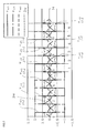
- FIGURE 1 is a functional block diagram showing a configuration of a control system according to a first embodiment (corresponding to the first to the third aspects) of the invention.
- the control system is formed with, for example, hardware and software of a microcomputer system.
- the embodiment will be explained as a control system controlling the previously explained three-level inverter shown in FIG. 14 .
- the embodiment can be also applied to the control of the three-level inverter shown in FIG. 13 .
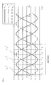
- FIGURE 2 is a waveform diagram showing the waveforms of three-phase output voltage commands v u *, v v * and v w * in the control system according to the first embodiment.
- reference numeral 10 denotes a maximum, middle and minimum voltage command operating means.
- the operating means 10 three-phase AC output voltage commands v u *, v v * and v w * as those shown in FIG. 2 are inputted which are obtained by operations performed on the basis of frequency commands, for example.
- the one period of each of the voltage commands is divided into six, from the section 1 to the section 6, for example.
- a middle phase selecting means 20 shown in FIG. 1 selects a voltage command, the value of which is a middle value, as a middle voltage command v mid from the inputted voltage commands v u *, v v * and v w *.
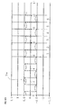
- the maximum, middle and minimum voltage command operating means 10 classifies the voltage commands v u *, v v * and v w * in each section by value into maximum voltage commands v max , middle voltage commands v mid , and minimum voltage commands v min as those shown in a discrimination table given as Table 1.
- the voltage commands v v *, v u * and v w * are to be arranged in their respective sections in the order of v v * ⁇ v u * ⁇ v w * so that the order is repeated in cycles.
- the maximum, middle and minimum voltage command operating means 10 shown in FIG. 1 carries out compensation in which each of the maximum voltage command v max , middle voltage command v mid and minimum voltage command v min in each of the sections shown in Table 1 has the middle voltage command v mid in the section subtracted therefrom as is expressed in the expressions (1) with the respective resulting outputs of a maximum voltage command v max *, middle voltage command v mid * and minimum voltage command v min *.
- FIGURE 3 is a waveform diagram showing the waveforms of voltage commands v u0 , v v0 and v w0 after the output voltage commands v u *, v v * and v w * shown in FIG. 2 are compensated according to the expressions (1).
- the maximum voltage command v max , middle voltage command v mid and minimum voltage command v min before being compensated by the expressions (1) are the output voltage command v u * in the U-phase, the output voltage command v v * in the V-phase and the output voltage command v w * in the W-phase, respectively, which are shown in Fig. 2 .
- the maximum voltage command v max * is designated as v u0 in the U-phase
- the minimum voltage command v min * is designated as v w0 in the W-phase.
- a compensated zero-phase voltage command 3w is also shown.
- the zero-phase voltage command 3w is a command derived by carrying out the compensation of subtracting the middle voltage command v mid from the zero-phase voltage with the value zero in the same way as is expressed in the expressions (1) with respect to each section in FIG. 2 .
- the zero-phase voltage is the reference voltage for a voltage in each phase, then, in a line-to-line voltage as a difference between a voltage in a certain phase and a voltage in another phase, the zero-phase voltages with respect to their respective voltages cancel out each other.
- the on-time ratio operating means 30 carries out operations by the following expressions (2) with the values of the maximum voltage command v max * and minimum voltage command v min * of the voltage commands and the values of the DC voltages Ed (DC high voltage) and -Ed (DC low voltage) in the DC circuit of the inverter to obtain on-time ratios ⁇ max * and ⁇ min *.
- the on-time ratio ⁇ max * is the ratio of a time, during which the switching element S 1 in the DC circuit in the inverter is turned-on for providing an output corresponding to the maximum voltage command v max *, to one switching period in the switching operation of converting the DC voltages to an AC voltage.
- the on-time ratios ⁇ max * and ⁇ min * are proportional to the voltage commands v max * and v min *, respectively.
- the value of ⁇ min * is provided as a positive one.
- the maximum voltage command v max is the voltage command v u * in the U-phase. Then, the maximum voltage command v max * after being compensated is the voltage command v u0 .
- the on-time ratio of the switching element S 1 which outputs the maximum voltage Ed in the DC circuit with respect to the U-phase in the three-level inverter shown in FIG. 14 , is provided as ⁇ max *. While, the switching element S 3 in the circuit is made to be turned-off while the switching element S 1 is turned-on and is made to be turned-on while the switching element S 1 is turned-off to output a voltage zero. Therefore, the on-time ratio thereof is provided as 1 - ⁇ max *.
- the switching element S 2 causing no short circuit in the DC power supply 102 even though it is turned-on, is made to be turned-on through the one switching period to be brought into a free-wheeling mode.
- the switching element S 4 since the DC circuit with respect to the U-phase outputs no minimum voltage -Ed in the section 1, is made to be turned-off through the one switching period.
- the voltage command v v * in the V-phase has a middle value.
- each of the switching element S 2 and S 3 is fixed in a turned-on state and each of the switching element S 1 and S 4 is fixed in a turned-off state without carrying out switching operation in the one switching period.
- the minimum voltage command v min is the voltage command v w * in the W-phase.
- the minimum voltage command v min * after being compensated is the voltage command v w0 . Therefore, the on-time ratio of the switching element S 4 , which outputs the minimum voltage -Ed in the DC circuit with respect to the W-phase, equivalent to the DC circuit with respect to the U-phase in the three-level inverter shown in FIG. 14 , is provided as ⁇ min *.
- the switching element S 2 in the circuit is made to be turned-off while the switching element S 4 is turned-on and is made to be turned-on while the switching element S 4 is turned-off to output a voltage zero.
- the on-time ratio thereof is provided as 1 - ⁇ min *. Furthermore, the switching element S 3 , causing no short circuit in the DC power supply 101 even though it is turned-on, is made to be turned-on through the one switching period to be brought into a free-wheeling mode. The switching element S 1 , since the DC circuit with respect to the W-phase outputs no maximum voltage Ed in the section 1, is made to be turned-off through the one switching period.
- a by-phase on-time ratio operating means 40 converts the on-time ratios ⁇ max *, ⁇ mid * and ⁇ min * in each of the foregoing sections, which ratios are inputted to the means 40 while being classified by value, into on-time ratios ⁇ u , ⁇ v and ⁇ w classified by phase of the U, V and W.
- the on-time ratios ⁇ max * and ⁇ min * are proportional to the maximum voltage command v max and v min *, respectively, and the value of the on-time ratio ⁇ mid * is zero in correspondence with the value of the middle voltage command v mid * being zero.
- the waveforms of the on-time ratios ⁇ u , ⁇ v and ⁇ w are geometrically similar to the waveforms of the voltage commands v u0 , v v0 and v w0 shown in FIG. 3 , respectively.
- the on-time ratios corresponding to the negative voltage commands become positive.
- a triangular wave comparing means 50 as a carrier comparison means compares the waveforms of the on-time ratios ⁇ u , ⁇ v and ⁇ w in their respective U-, V- and W-phases with a triangular wave as a carrier to obtain on-off commands for the switching elements in the DC circuit of the inverter in each of the U-, V- and W-phases from the result of the comparison and outputs the obtained commands.
- signs S u1 to S w4 designate on-off commands outputted from the triangular wave comparing means 50.
- the on-off commands S u1 to S w4 are the on-off commands to four switching elements (corresponding to the switching elements S 1 to S 4 shown in FIG. 14 ) in the DC circuit in the U-phase
- the on-off commands S v1 to S v4 are the on-off commands to four switching elements in the DC circuit in the V-phase not shown
- the on-off commands S w1 to S w4 are the on-off commands to four switching elements in the DC circuit in the W-phase not shown.
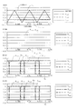
- FIGURE 4 is a waveform diagram showing the operation of the triangular wave comparing means 50 according to the first embodiment in a part of the section 1 with (a) showing the waveforms of the on-time ratios ⁇ u , ⁇ v , ⁇ w in the U-, V- and W-phases, respectively, together with the waveform of the triangular wave as a carrier, (b) showing the waveforms of the on-off commands S u1 to S u4 to the switching elements in the inverter in the U-phase, (c) showing the waveforms of the on-off commands S v1 to S v4 to the switching elements in the inverter in the V-phase, (d) showing the waveforms of the on-off commands S w1 to S w4 to the switching elements in the inverter in the W-phase.
- FIG. 4 show the turned-on and -off states of the switching elements in the U-, V- and W-phases, respectively.
- a part of the section 1 is the part from 0.3 to 0.32 in the section 1 when letting the length (time length) of the section 1 shown in FIG. 2 and FIG. 3 be unity.
- the reference signs of the on-off commands S u1 to S u4 , S v1 to S v4 and S w to S w4 are to be also used as the reference signs of the switching elements.
- a carrier of a triangular wave is formed which moves between 0 and 1 as is shown in (a) of FIG. 4 .
- the time length from the time at which the carrier initiates an increase from zero to the time at which the carrier returns to zero again after reaching 1 and then turning back therefrom becomes the one switching period.
- the triangular wave comparing means 50 shown in FIG. 1 is formed by using a comparator contained in a device such as a microcomputer, with which means the values of the on-time ratios ⁇ u , ⁇ v and ⁇ w , corresponding to the values of the waveforms of the voltage commands ⁇ u0 , v v0 , v w0 in the U-, V- and W-phases shown in FIG. 3 , respectively, are compared with the value of the triangular wave as a carrier as is shown in (a) of FIG. 4 .
- the period of the triangular wave is equivalent to the one switching period of the switching element.
- the on-time ratios ⁇ u , ⁇ v and ⁇ w are shown as the on-time ratio ⁇ max * corresponding to the voltage command v u0 as the maximum voltage command v max *, the on-time ratio ⁇ mid * corresponding to the voltage command v v0 as the middle voltage command ⁇ mid * and the on-time ratio ⁇ min * corresponding to the voltage command v w0 as the minimum voltage command v min *, respectively.
- the on-time ratio ⁇ w shown as the on-time ratio ⁇ min * corresponding to the voltage command v w0 as the negative minimum voltage command ⁇ min *, is shown as being positive according to the expressions (2).
- the time during which the value of the on-time ratio is equal to or more than the value of the triangular wave in the period of the triangular wave, i.e. the one switching period of a switching element is determined as the time during which the switching element is made turned-on with the on-time ratio by an on-off command.
- the triangle is formed by the triangular wave and a straight line intersecting the triangular wave and representing, for example, the on-time ratio ⁇ u in the U-phase as the on-time ratio ⁇ max *.
- the triangle is one with the straight line that represents the on-time ratio ⁇ u ( ⁇ max *) forming a base and the on-time ratio ⁇ u ( ⁇ max *) therefore being the height thereof.
- the ratio of the time, during which the value of the on-time ratio ⁇ u ( ⁇ max *) is equal to or more than the value of the carrier, to the one switching period is the on-time ratio ⁇ max *.
- the time in the rest of the one period of the carrier, during which the value of the on-time ratio ⁇ u ( ⁇ max *) is less than the value of the carrier, is proportional to the on-time ratio 1 - ⁇ max *.
- on-off commands each having a determined on-time ratio, are formed with respect to each of the phases as is shown in (b), (c) and (d) of FIG. 4 .
- the voltage command v u0 in the U-phase is the maximum voltage command ⁇ max *. Therefore, in (b) of FIG. 4 , waveforms of the on-off commands S u1 to S u4 , which are for carrying out switching of the switching elements S u1 to S u4 in the U-phase with the on-time ratios ⁇ maxS1 to ⁇ maxS4 , respectively, being provided by the expressions (3), are shown in the part of the section 1.
- the value of the on-off command S u1 becomes 1 from 0 with the on-time ratio ⁇ maxS1 provided as ⁇ max * as the on-time ratio ⁇ u by the expressions (3). Simultaneously with this, the value of the on-off command S u3 becomes 0 from 1.
- the value of the on-off commands S u1 becomes 0.
- the on-off commands S u3 becomes to have the value of 1 with the on-time ratio ⁇ maxS3 provided as 1 - ⁇ max * by the expressions (3) and becomes to have the value 0 again at the end of the one switching period, i.e. at the beginning of the next one switching period.
- the value of the on-off command S u1 becomes 1 again from 0.
- each of the switching elements S u1 and S u3 carry out two times of switching, four times in total of both, in the one switching period (the switching elements S u1 is made to be turned-on, then turned-off and then turned-on and the switching element S u3 is made to be turned-off, then turned-on and then turned-off).
- waveforms of the on-off commands S v1 to S v4 which are for carrying out switching of the switching elements S v1 to S v4 in the V-phase with the on-time ratios ⁇ midS1 to ⁇ midS4 , respectively, being provided by the expressions (4), are shown in the part of the section 1.
- waveforms of the on-off commands S v1 to S v4 which are for carrying out switching of the switching elements S v1 to S v4 in the V-phase with the on-time ratios ⁇ midS1 to ⁇ midS4 , respectively, being provided by the expressions (4), are shown in the part of the section 1.
- the waveforms (characteristic lines) of the on-off commands S v3 and S v2 to their respective switching elements S v3 and S v2 coincide with each other and the waveforms (characteristic lines) of the on-off commands S v4 and S v1 to their respective switching elements S v4 and S v1 coincide with each other.
- the characteristic lines are shown as those for the switching elements S v3 and S v4 only.
- the voltage command v w0 in the W-phase is the minimum voltage command v min *. Therefore, in (d) of FIG. 4 , waveforms of the on-off commands S w1 to S w4 , which are for carrying out switching of the switching elements S w1 to S w4 in the W-phase with the on-time ratios ⁇ minS1 to ⁇ minS4 , respectively, being provided by the expressions (5), are shown in the part of the section 1.
- the value of the on-off command S w4 becomes 1 from 0 with the on-time ratio ⁇ minS4 provided as ⁇ min * as the on-time ratio ⁇ w by the expressions (5). Simultaneously with this, the value of the on-off command S w2 becomes 0 from 1.
- the value of the on-off commands S w4 becomes 0.
- the on-off commands S w2 becomes to have the value of 1 with the on-time ratio ⁇ minS2 provided as 1 - ⁇ min * by the expressions (5) and becomes to have the value 0 again at the end of the one switching period, i.e. at the beginning of the next one switching period.
- the value of the on-off command S w2 becomes 1 again from 0.
- each of the switching elements S w2 and S w4 carry out two times of switching, four times in total of both, in the one switching period like the switching elements S u1 and S u3 in the U-phase.
- a train of rectangular waves each with an on-time ratio changing with time that is, a train of rectangular waves each with a width proportional to the value of the compensated voltage command changing with time, are formed with respect to each of three phases of the U-, V- and W-phases.
- the train of the rectangular waves are subjected to known demodulating processing to be converted into a three-level AC voltage.
- the three-level inverter can be controlled by carrying out switching of eight times per switching period.
- the carrier of the triangular wave which is used for outputting the on-off commands in the U- V- and W-phases with the predetermined on-time ratios ⁇ u , ⁇ v and ⁇ w , respectively, in each section, can be produced by an up-down counter contained in a device such as a common microcomputer. This requires no high performance and high expensive operation device to make it possible to avoid an increase in cost.
- inverter it is possible to reduce switching losses by reducing the number of times of switching and, along with this, to lower the cost of the control system with the use of an inexpensive device such as a microcomputer.
- the control system according to the first embodiment has the following problem. Namely, the voltage command after being compensated and shown in FIG. 3 has an amplitude ( ⁇ 0.75 in the embodiment) larger than the amplitude ( ⁇ 0. 5 in the embodiment) of the voltage command shown in FIG. 2 which is inputted to the control system. Therefore, when the amplitude of the inputted voltage command becomes large, the value of the maximum voltage command v max * after being compensated and the absolute value of the minimum voltage command v mm * after being compensated are sometimes calculated as being larger than the absolute value E d of the power supply voltage to cause the values of the on-time ratios ⁇ max * and ⁇ min * to exceed 1.
- a control system is actualized in which the range of the voltage that can be normally outputted is expanded with the number of times of switching equal to that in the first embodiment.
- FIGURE 5 is a functional block diagram showing a configuration of a control system according to a second embodiment (corresponding to the fourth to the sixth aspects) of the invention.
- the control system like the control system according to the first embodiment, is formed with hardware and software of a microcomputer system. Also the embodiment will be explained as a control system of the three-level inverter shown in FIG. 14 . The embodiment, however, can be of course applied also to the control of the three-level inverter shown in FIG. 13 .
- FIGURE 6 is a waveform diagram showing the waveforms of three-phase output voltage commands v u *, v v * and v w * in the control system according to the second embodiment.
- FIG. 5 constituents with similar functions to those of constituents shown in FIG. 1 will be denoted with similar reference numerals and signs. In the following, explanations will be made with particular emphasis on parts different from those shown in FIG. 1 .
- reference numeral 60 denotes a maximum, middle and minimum voltage command operating means, to which three-phase AC output voltage commands v u *, v v * and v w * shown in FIG. 6 are inputted like in the first embodiment.
- an absolute maximum value command discriminating means 70 detects a voltage command having an absolute maximum value as an absolute maximum voltage command v max . From the detected absolute maximum voltage command v max * and the polarity (sign) thereof, the absolute maximum value command discriminating means 70 further obtains an absolute maximum voltage command v 0 * as a compensation value to be explained later and output it to the maximum, middle and minimum voltage command operating means 60.
- the one period of each of the voltage commands is divided into six, from the section 1 to the section 6.
- the maximum, middle and minimum voltage command operating means 60 determines a phase with stopped switching and a voltage level produced in the phase before carrying out operations for obtaining v max *, v mid * and v mm * as being maximum, middle and minimum voltage commands, respectively, which will be explained later.
- Table 2 SECTION ABSOLUTE MAX.
- the voltage command v u * in the U-phase has the maximum value with the absolute value thereof also being maximum compared with the voltage command v v * in the V-phase and the voltage command v w * in the W-phase. Therefore, of the switching elements connected to the U-phase output terminal in the DC circuit shown in FIG. 14 , the switching element S 1 between the U-phase output terminal and the DC high voltage E d is made to be turned-on over one switching period to thereby produce the voltage E d at the U-phase output terminal. At this time, the switching elements S 3 and S 4 are made to be turned-off for preventing the DC power supply from being short-circuited and the switching element S 2 is made to be turned-on for being brought into a fly-wheeling mode.
- the voltage command v w * in the W-phase has the minimum value with the absolute value thereof being maximum compared with the voltage command v u * in the U-phase and the voltage command v v * in the V-phase. Therefore, of the switching elements connected to the W-phase output terminal in the DC circuit shown in FIG. 14 , the switching element S 4 between the W-phase output terminal and the low DC voltage -E d (Although FIG. 14 shows the DC circuit in the U-phase, the DC circuit in the W-phase has a configuration identical to the DC circuit shown in FIG. 14 .
- the switching element is to be denoted as S 4 here) is made to be turned-on over one switching period to thereby produce the voltage -E d at the W-phase output terminal.
- the switching elements S 1 and S 2 are made to be turned-off for preventing the DC power supply from being short-circuited and the switching element S 3 is made to be turned-on for being brought into a fly-wheeling mode.
- the maximum, middle and minimum voltage command operating means 60 classifies the original output voltage commands v u *, v v * and v w * by value into an absolute maximum voltage command v max , a middle voltage command v mid and a minimum voltage command v min in each section like in the first embodiment. With respect to thus classified voltage commands, the maximum, middle and minimum voltage command operating means 60 carries out operations of compensating them with the absolute maximum voltage command v 0 * obtained by the expression (6) as are expressed by the following expressions (7) to obtain a maximum voltage command v max *, a middle voltage command v mid * and a minimum voltage command v min *.
- FIGURE 7 is a waveform diagram showing the waveforms of voltage commands v u0 , v v0 and v w0 after the output voltage commands v u *, v v * and v w * shown in FIG. 2 are compensated according to the expressions (7).
- the waveforms of the voltage commands v u0 , v v0 and v w0 shown in FIG. 7 are shown in FIG. 8A , FIG. 8B and FIG. 8C , respectively.
- FIG. 8D shows only a zero-phase voltage command 3w shown in FIG. 7 .
- the zero-phase voltage is the reference voltage for a voltage in each phase
- the zero-phase voltages with respect to their respective voltages cancel out each other. Therefore, in each of the voltage commands v u0 , v v0 and v w0 which is provided as the difference between the voltage command in a certain phase and the voltage command in another phase as is expressed in the expressions (7), the zero-phase voltage commands 3w cancel out each other.
- the control of an output voltage according to each of the voltage commands v u0 , v v0 and v w0 will be unaffected by the zero-phase voltage command 3w.
- the value of the maximum voltage command v max * is 1 or -1 when letting the value of the voltage E d be 1.
- the maximum voltage command v max * the voltage command v u0 with the value 1 in the U-phase is outputted in the section 1
- the voltage command v w0 with the value -1 in the W-phase is outputted in the section 2
- the voltage command v v0 with the value 1 in the V-phase is outputted in the section 3.
- an on-time ratio operating means 30 the maximum voltage command v max *, middle voltage command v mid * and minimum voltage command v min * in each section are inputted which are those after being compensated.
- the on-time ratio operating means 30 carries out operations by the following expressions (8) with the values of the middle voltage command v mid * and minimum voltage command v min * of the voltage commands and the values of the DC voltages Ed and -Ed in the DC circuit of the inverter to obtain on-time ratios ⁇ mid * and ⁇ min *.
- the on-time ratio ⁇ mid * is the ratio of a time, during which the switching element in a phase with the absolute value of the middle voltage command v mid * being a middle value (hereinafter referred to as an "absolute middle value phase”) is turned-on, to the one switching period.
- the on-time ratios ⁇ max * and ⁇ min * are proportional to the absolute value of the middle voltage command v max * and the absolute value of the minimum voltage command v min *, respectively.
- the on-time ratio ⁇ max * becomes 1 when the maximum voltage command v max * is positive, with which the switching element S 1 is made to be turned-on, and becomes 0 when the maximum voltage command v max * is negative, with which the switching element S 4 is made to be turned-on.
- the voltage command v u0 in the U-phase is the maximum voltage command v max * with the absolute value thereof being maximum.
- the on-time ratio of the switching element S 1 becomes 1 in the DC circuit with respect to the U-phase in an inverter shown in FIG.14 .
- the on-time ratios of the switching elements S 3 and S 4 become zero and the on-time ratio of the switching element S 2 becomes 1.
- the voltage command v w0 in the W-phase is the maximum voltage command v max * in the absolute maximum value phase with the polarity thereof being negative.
- the middle voltage command v mid * in the absolute middle value phase shifts from the voltage command v w0 in the W-phase to the voltage command v v0 in the V-phase with the polarities thereof being positive. Therefore, switching is carried out between the DC high voltage E d and the DC middle voltage, i.e. zero voltage.
- the minimum voltage command v min * in the absolute minimum value phase shifts from the voltage command v v0 in the V-phase to the voltage command v w0 in the W-phase with the polarities thereof being negative. Therefore, switching is carried out between the DC middle voltage, i.e. zero voltage and the DC low voltage -E d .
- the on-time ratio operating means 30 shown in FIG. 5 outputs the on-time ratios ⁇ max *, ⁇ mid * and ⁇ min * obtained from the inputted maximum voltage command v max *, middle voltage command v mid * and minimum voltage command v min *, respectively.
- a by-phase on-time ratio operating means 40 converts the on-time ratios ⁇ max *, ⁇ mid * and ⁇ min * in each of the foregoing sections, which ratios are inputted to the means 40 while being classified by value, into on-time ratios ⁇ u , ⁇ v and ⁇ w classified by phase of the U, V and W.
- the on-time ratios ⁇ mid * and ⁇ min * are proportional to the middle voltage command v mid * and the minimum voltage command v min *, respectively, and the value of the on-time ratio ⁇ max * is 1 or zero.
- the waveforms of the on-time ratios ⁇ u , ⁇ v and ⁇ w are geometrically similar to the waveforms of the voltage commands v u0 , v v0 and v w0 shown in FIGS. 8A , 8B and 8C , respectively.
- the on-time ratios corresponding to the negative voltage commands become positive.
- a triangular wave comparison means 50 as a carrier comparison means compares the waveforms of the on-time ratios ⁇ u , ⁇ v and ⁇ w in their respective U-, V- and W-phases with a triangular wave as a carrier to obtain on-off commands for the switching elements in the DC circuit of the inverter in each of the U-, V- and W-phases from the result of the comparison and outputs the obtained commands.
- signs S u1 to S w4 designate on-off commands outputted from the triangular wave comparison means 50.
- the on-off commands S u1 to S w4 are the on-off commands to four switching elements (corresponding to the switching elements S 1 to S 4 shown in FIG. 14 ) in the DC circuit in the U-phase
- the on-off commands S v1 to S v4 are the on-off commands to four switching elements in the DC circuit in the V-phase not shown
- the on-off commands S w1 to S w4 are the on-off commands to four switching elements in the DC circuit in the V-phase not shown.
- FIGURE 9 is a waveform diagram showing the operation of the triangular wave comparing means 50 according to the second embodiment in a part of the section 1 with (a) showing the waveforms of the on-time ratios ⁇ u , ⁇ v , ⁇ w in the U-, V- and W-phases, respectively, together with the waveform of the triangular wave as a carrier, (b) showing the waveforms of the on-off commands S u1 to S u4 to the switching elements in the inverter in the U-phase, (c) showing the waveforms of the on-off commands S v1 to S v4 to the switching elements in the inverter in the V-phase, (d) showing the waveforms of the on-off commands S w1 to S w4 to the switching elements in the inverter in the W-phase.
- FIG. 9 show the turned-on and -off states of the switching elements in the U-, V- and W-phases, respectively.
- a part of the section 1 is the part from 0 to 0. 02 in the section 1 when letting the length (time length) of the section 1 shown in FIG. 6 to FIG. 8D be unity.
- the reference signs of the on-off commands S u1 to S u4 , S v1 to S v4 and S w1 to S w4 are to be also used as the reference signs of the switching elements.
- a carrier of a triangular wave is formed which moves between 0 and 1 as is shown in (a) of FIG. 9 .
- the time length from the time at which the carrier initiates an increase from zero to the time at which the carrier returns to zero again after reaching 1 and then turning back therefrom becomes the one switching period.
- the triangular wave comparison means 50 shown in FIG. 5 is also formed by using a comparator contained in a device such as a microcomputer, with which means the values of the on-time ratios ⁇ u , ⁇ v and ⁇ w , corresponding to the values of the waveforms of the voltage commands v u0 , v v0 , v w0 in the U-, V- and W-phases shown in FIGS. 8A to 8C , respectively, are compared with the value of the triangular wave as a carrier as is shown in (a) of FIG. 9 .
- the period of the triangular wave is equivalent to the one switching period of the switching element.
- the on-time ratio ⁇ v is shown as the on-time ratio ⁇ min * corresponding to the voltage command v v0 as the minimum voltage command v min * before the voltage command v v0 is shifted to the middle voltage command v mid *
- the on-time ratio ⁇ w is shown as the on-time ratio ⁇ mid * corresponding to the voltage command v w0 as the minimum voltage command v mid * before the voltage command v w0 is shifted to the minimum voltage command v min *.
- the on-time ratio ⁇ v as the on-time ratio ⁇ min * corresponding to the voltage command v v0 being the negative minimum voltage command v min * is shown as being positive according to the expressions (8).
- the part of the section 1 shown in FIG. 9 is the part from 0 to 0.02 to the 1 as the length of the section 1, i.e. a very short part of only 2% of the section 1. Therefore, in such a short part, the waveform of the on-time ratio can be regarded as a straight line approximately representing a constant value and in parallel to the horizontal axis.
- the time during which the value of the on-time ratio is equal to or more than the value of the carrier in the one switching period of the carrier i.e. the one switching period of a switching element, is determined as the time during which the switching element is made turned-on with the on-time ratio by an on-off command.
- on-off commands each having a determined on-time ratio, are formed with respect to each of the phases as is shown in (b), (c) and (d) of FIG. 9 .
- waveforms of the on-off commands S v1 to S v4 which are for carrying out switching of the switching elements S v1 to S v4 in the V-phase with the on-time ratios ⁇ midS1 to ⁇ midS4 , respectively, being provided by the expressions (11), are shown in the part of the section 1.
- each of the switching elements S v1 and S v3 carry out two times of switching, four times in total of both, in the one switching period.
- waveforms of the on-off commands S w1 to S w4 which are for carrying out switching of the switching elements S w1 to S w4 in the W-phase with the on-time ratios ⁇ minS1 to ⁇ minS4 , respectively, being provided by the expressions (12), are shown in the part of the section 1.
- each of the switching elements S w2 and S w4 carry out two times of switching, four times in total of both, in the one switching period like the switching elements S u1 and S u3 in the U-phase.
- a train of rectangular waves each with an on-time ratio changing with time that is, a train of rectangular waves each with a width proportional to the value of the compensated voltage command changing with time, are formed with respect to each of three phases of the U-, V- and W-phases.
- the train of the rectangular waves are subjected to known demodulating processing to be converted into a three-level AC voltage.
- the three-level inverter can be controlled by carrying out switching of eight times per switching period.
- the carrier of the triangular wave can be easily produced to make it possible to form the control device at a low cost.
- FIGURE 10 is a waveform diagram showing the waveforms of the voltage commands v u0 , v v0 and v w0 after the output voltage commands v u *, v v * and v w * shown in FIG. 2 are compensated with their respective amplitudes increased from illustrated 0.5 to 0.8 (letting the DC voltage be 1, from 50% to 80% to the DC voltage) in the first embodiment.
- FIGURE 11 is a waveform diagram showing the waveforms of voltage commands v u0 , v v0 and v w0 after the compensation according to the second embodiment is carried out with respect to the output voltage commands v u *, v v * and v w * shown in FIG. 6 with their respective amplitudes similarly increased from illustrated 0.5 to 0.8.
- each of the voltage commands v u0 , v v0 and v w0 are outside the range of -1 to 1, that is, outside the DC power supply voltage ranging from -E d to E d . Since the inverter cannot outputs a voltage with the absolute value thereof being larger than the power supply voltage E d , the part of the voltage command with the value thereof exceeding 1 or -1 cannot produce voltages according to the command. This means that the output voltages are saturated to be distorted.
- the compensation in the first embodiment is carried out so as to add a middle voltage command in the phase with the middle voltage command to a voltage commands in other phases as is expressed in the expressions (1) with the switching made stopped in the phase with the middle voltage command. That is, this is because in the phase with the maximum voltage command, an increased amplitude of the voltage command sometimes causes the value of the voltage command after the compensation to become larger than the value of the original maximum voltage command and exceed 1 by the addition.
- the value of the zero-phase voltage command 3w is smaller than that in the second embodiment, which provides the advantage of small potential variations in the zero-phase as a common mode that cause small noises.
- a discriminating means is provided for carrying out switching so that, with respect to the region in which the ratio of the amplitude as the maximum value of the voltage command to the DC power supply voltage is equal to or less than 0.6, the control of output voltages is carried out with the on-time ratios determined by the operations according to the first embodiment and, with respect to the region in which the ratio is more than 0.6, the control of output voltages is carried out with the on-time ratios determined by the operations according to the second embodiment.
- the foregoing ratio 0.6 is a rough measure, which can be corrected with the voltage drops in the semiconductor switching elements and errors in detection circuits in detection circuits taken into consideration.
- the switching between control according to the first embodiment and the control according to the second embodiment switches the operation procedures of the voltage commands. Then, operations of the voltages commands according to both of the embodiments are not simultaneously carried out in parallel to cause no fear of increasing the burden of operational processing in a microcomputer. Furthermore, since the foregoing switching is carried out only by switching between voltage commands to be compared with the carrier, no shock due to pulses is generated at switching.
Landscapes
- Engineering & Computer Science (AREA)
- Power Engineering (AREA)
- Inverter Devices (AREA)
Abstract
Description
- The present invention relates to a control method and a control system in a three-level inverter which outputs an AC voltage in three levels converted from a DC voltage by carrying out the switching of the DC voltage with the use of semiconductor switching elements, the control method and the control system enabling the inverter to reduce the number of times of the switching and to expand the range of the output voltage.
-
FIGURE 13 is a circuit diagram showing the circuit configuration of an example of a common three-level inverter with respect to the circuit of one phase. Here, for simplifying the explanation, the circuit configuration with respect to only one phase (U-phase) of the output circuits of three phases is shown. - In
FIG. 13 , the three-level inverter is provided withDC power supplies 101 and 102 (letting each of the voltage values thereof be Ed), semiconductor switching elements S1 to S4 such as IGBTs and diodes D1 and D2. Signs N and U designate a neutral point and an output terminal, respectively. In the following explanations, in a DC circuit, the positive electrode of theDC power supply 101, the negative electrode of theDC power supply 102 and the neutral point N are to be also referred to as a high voltage point, a low voltage point and a middle voltage point, respectively. Moreover, the voltage Ed, the voltage -Ed and avoltage 0 are to be referred to as a DC high voltage, a DC low voltage and a DC middle voltage, respectively. - In the three-level inverter, by the turning-on and -off operations of the semiconductor switching elements S1 to S4 connected in series and the action of the diodes D1 and D2, it is possible to output the voltages at three levels in the DC circuit, namely the voltages Ed, 0, and - Ed (here, the voltages drop at each element is ignored).
- For example, with the semiconductor switching elements S1 and S2 being turned-on and the semiconductor switching elements S3 and S4 being turned-off, an output voltage becomes Ed, with the semiconductor switching elements S2 and S3 being turned-on and the semiconductor switching elements S1 and S4 being turned-off, an output voltage becomes 0, and with the semiconductor switching elements S3 and S4 being turned-on and the semiconductor switching elements S1 and S2 being turned-off, an output voltage becomes -Ed.
-
FIGURE 14 is a circuit diagram showing the circuit configuration of another example of a common three-level inverter with respect to the circuit of one phase. - In
FIG. 14 , the configuration of the circuit of a three-level inverter is shown with respect to one phase in which inverter the diodes D1 and D2 in the three-level inverter shown inFIG. 13 are omitted and a bidirectional switch S23 formed of the semiconductor switching elements S2 and S3 is used. - The levels of the output voltages of the three-level inverter are the same as the levels of the output voltages of the three-level inverter shown in
FIG. 13 . For example, with the semiconductor switching element S1 being turned-on and with the semiconductor switching elements S2 to S4 being turned-off, the output voltage becomes Ed, with the semiconductor switching elements S2 and S3 being turned-on and with the semiconductor switching elements S1 and S4 being turned-off, the output voltage becomes 0, and with the semiconductor switching element S4 being turned-on and with the semiconductor switching elements S1 to S3 being turned-off, the output voltage becomes -Ed. - In this way, the three-level inverter, by outputting voltages at three levels, can relax an abrupt change in a voltage applied to a load compared with a two-level inverter. In particular, when a motor is connected as a load, such a three-level inverter is effective in inhibiting a surge voltage to allow the three-level inverter to be widely used.
- Here, for a control method of a three-level inverter, there is the method described in each of
JP-A-2007-282484 FIG. 1 to FIG. 3 , etc.) andJP-A-2010-206931 FIG. 1 to FIG. 3 , etc.). - In
JP-A-2007-282484 FIG. 3 , etc.), a method is described in which an output voltage is provided on the basis of the frequency command or the amplitude command of an output voltage command with a dipolar modulation method carried out in a low output voltage region, a unipolar modulation method carried out in a middle output voltage region and an over modulation method carried out in a high output voltage region other than the former two regions, and control is carried out by switching the modulation methods according to the output voltage region. - In
JP-A-2010-206931 FIG. 1 to FIG. 3 , etc.), a control method is disclosed in which a plurality of output voltage vectors suited for an output voltage command are selected with the use of instantaneous space vectors and the selected vectors are made to be outputted in the order for preventing common mode voltages, with suggestion of making the voltage vectors cause transition so as not to increase the number of switching operations more than that being necessary. -
- [Patent Document 1]
JP-A-2007-282484 FIG. 1 to FIG. 3 , etc.) - [Patent Document 2]
JP-A-2010-206931 FIG. 1 to FIG. 3 , etc.) - In the related three-level inverter described in
JP-A-2007-282484 - While, in the dipolar modulation method, there is a problem in that the number of switching operations is to further increase in the low output voltage region to lower the efficiency of a system due to switching losses.
- In addition, according to the related three-level inverter described in
JP-A-2010-206931 - Accordingly, it is an object of the invention to provide a control method and a control system of a three-level inverter which are intended for downsizing and high efficiency with reduced losses by reducing the number of switching operations against the problem of the three-level inverter described in
JP-A-2007-282484 JP-A-2010-206931 - For solving the foregoing problems, a first aspect of the invention is that in a control method of a three-level inverter wherein, with respect to a configuration in which three of three-level inverters are connected in parallel to each other,
the three level inverter carrying out turning-on and -off of a plurality of semiconductor switching elements of
at least one semiconductor switching element connected between a high voltage point of a DC circuit and one output terminal,
at least one semiconductor switching element connected between a middle voltage point of the DC circuit and the output terminal, and
at least one semiconductor switching element connected between a low voltage point of the DC circuit and the output terminal, and
enabling any one of three level voltages of a DC high voltage, DC middle voltage and DC low voltage as the base of an AC voltage for one-phase to be outputted from the output terminal,
the method makes a plurality of the semiconductor switching elements in each of the three three-level inverters turned-on and -off on the basis of output voltage commands of three-phase AC voltages to thereby make the three-phase AC voltage outputted, the method includes the steps of:
carrying out operations for obtaining on-time ratios of a plurality of the semiconductor switching elements in each of the three three-level inverters on the basis of the output voltage commands of the three-phase AC voltages;
dividing the one period of the output voltage command of the three-phase AC voltage into a plurality of sections; and
in each of the sections,
making the three-level inverter for one-phase alternately turn-on and -off the at least one semiconductor switching element connected between the high voltage point and the output terminal and the at least one semiconductor switching element connected between the middle voltage point and the output terminal with their respective operated on-time ratios in one switching period of the semiconductor switching element to alternately output the DC high voltage and the DC middle voltage;
along with this, making the three-level inverter for another one-phase fix the at least one switching element connected between the middle voltage point and the output terminal in a turned-on state to output the DC middle voltage; and
along with this, further making the three-level inverter for the rest one-phase alternately turn-on and -off the at least one semiconductor switching element connected between the middle voltage point and the output terminal and the at least one semiconductor switching element connected between the low voltage point and the output terminal with their respective operated on-time ratios in the one switching period to alternately output the DC middle voltage and the DC low voltage. - A second aspect is that in the control method as the first aspect, the method includes the steps of:
- in each of the sections,
- with respect to a phase with the value of the output voltage command being a maximum value, carrying out compensation of subtracting a middle value of the output voltage command in another phase from the maximum value to provide thus compensated value as the value of a maximum voltage command in the phase in the section;
- with respect to the phase with the value of the output voltage command being the middle value, carrying out compensation of providing 0 as the value of a middle voltage command in the phase in the section;
with respect to the rest phase with the value of the output voltage command being a minimum value, carrying out compensation of subtracting the middle value of the output voltage command from the minimum value to provide thus compensated value as the value of a minimum voltage command in the phase in the section;
with respect to the phase with the value of the output voltage command being the minimum value, carrying out an operation of dividing the value of the maximum voltage command by the value of the DC high voltage to provide the on-time ratio of the at least one semiconductor switching element connected between the high voltage point and the output terminal in the three-level inverter in the phase and the on-time ratio of the at least one semiconductor switching element connected between the middle voltage point and the output terminal in the three-level inverter on the basis of the result of the division;
with respect to the phase with the value of the output voltage command being the middle value, carrying out an operation of providing 1 as the on-time ratio of fixing the at least one semiconductor switching element connected between the middle voltage point and the output terminal in the turned-on state in the three-level inverter in the phase on the basis of thevalue 0; and
with respect to the phase with the value of the output voltage command being the minimum value, carrying out an operation of dividing the value of the minimum voltage command by the value of the DC low voltage to provide the on-time ratio of the at least one semiconductor switching element connected between the middle voltage point and the output terminal in the three-level inverter in the phase and the on-time ratio of the at least one semiconductor switching element connected between the minimum voltage point and the output terminal in the three-level inverter on the basis of the result of the division. - A third aspect is a control system for carrying out the control method of the first or second aspect which system includes:
- a middle phase selecting means selecting, in each of the sections, an output voltage command of a phase with the value thereof being a middle value from the output voltage commands of the three-phase AC voltage;
- a maximum, middle and minimum voltage command operating means classifying, in each of the sections, the output voltage commands of the three-phase AC voltage by value into a voltage command of a phase with the value thereof being a maximum value, the selected voltage command of the phase with the value thereof being the middle value and a voltage command of a phase with the value thereof being a minimum value, and carrying out the compensation of subtracting the selected middle value from each of the classified output voltage commands to output the compensated results as a maximum voltage command, a middle voltage command with zero value and a minimum voltage command;
- an on-time ratio operating means carrying out, in each of the sections, an operation of dividing the value of the inputted maximum voltage command by the value of the DC high voltage to output the result of the operation as an operated value of the on-time ratio of the at least one semiconductor switching element connected between the high voltage point of the DC circuit and the one output terminal, carrying out an operation of converting the
value 0 of the inputted middle voltage command intovalue 1 to output thevalue 1 as an operated value of the on-time ratio of fixing the at least one semiconductor switching element connected between the middle voltage point of the DC circuit and the one output terminal in the turned-on state, and carrying out an operation of dividing the value of the inputted minimum voltage command by the value of the DC low voltage to output the result of the operation as an operated value of the on-time ratio of the at least one semiconductor switching element connected between the low voltage point of the DC circuit and the one output terminal; - a by-phase on-time ratio operating means classifying by phase, in each of the sections, the operated values of the on-time ratios, which are classified by values, and outputting the operated values classified by phase as voltages with the values thereof corresponding to the on-time ratios; and
- a carrier comparing means making, in each of the sections, the voltages, inputted by phase with the values thereof corresponding to the on-time ratios, compared with a carrier, which converts the compared voltage into an on-off command with an on-time ratio corresponding to the compared voltage, to produce on-off commands with the on-time ratios by phase and provide the on-off commands as those for a plurality of the semiconductor switching elements in each of the three three-level inverters.
- A fourth aspect is that in a control method of a three-level inverter wherein, with respect to a configuration in which three of three-level inverters are connected in parallel to each other,
the three level inverter carrying out turning-on and -off of a plurality of semiconductor switching elements of
at least one semiconductor switching element connected between a high voltage point of a DC circuit and one output terminal,
at least one semiconductor switching element connected between a middle voltage point of the DC circuit and the output terminal, and
at least one semiconductor switching element connected between a low voltage point of the DC circuit and the output terminal, and
enabling any one of three level voltages of a DC high voltage, DC middle voltage and DC low voltage as the base of an AC voltage for one-phase to be outputted from the output terminal,
the method makes a plurality of the semiconductor switching elements in each of the three three-level inverters turned-on and -off on the basis of output voltage commands of three-phase AC voltages to thereby make the three-phase AC voltage outputted, the method includes the steps of:
carrying out operations for obtaining on-time ratios of a plurality of the semiconductor switching elements in each of the three three-level inverters on the basis of the output voltage commands of the three-phase AC voltages;
dividing the one period of the output voltage command of the three-phase AC voltage into a plurality of sections; and
in each of the sections,
making the three-level inverter for one-phase fix one of the at least one semiconductor switching element connected between the high voltage point and the output terminal and the at least one semiconductor switching element connected between the low voltage point and the output terminal in a turned-on state to output one of the DC high voltage and the DC low voltage;
along with this, making the three-level inverter for another one-phase alternately turn-on and -off one of the at least one semiconductor switching element connected between the high voltage point and the output terminal and the at least one semiconductor switching element connected between the low voltage point and the output terminal with the at least one semiconductor switching element connected between the middle voltage point and the output terminal with their respective operated on-time ratios in one switching period of the semiconductor switching element to alternately output one of the DC high voltage and the DC low voltage with the DC middle voltage; and
along with this, when making the three-level inverter for another one-phase output the DC high voltage, further making the three-level inverter for the rest one-phase alternately turn-on and-off the at least one semiconductor switching element connected between the low voltage point and the output terminal and the at least one semiconductor switching element connected between the middle voltage point and the output terminal with their respective operated on-time ratios in one switching period of the semiconductor switching element to alternately output the DC low voltage with the DC middle voltage; and
when making the three-level inverter for another one-phase output the DC low voltage, further making the three-level inverter for the rest one-phase alternately turn-on and -off the at least one semiconductor switching element connected between the high voltage point and the output terminal and the at least one semiconductor switching element connected between the middle voltage point and the output terminal with their respective operated on-time ratios in one switching period of the semiconductor switching element to alternately output the DC high voltage with the DC middle voltage. - A fifth aspect is that in the control method as the fourth aspect, the method includes the steps of:
- in each of the sections,
- when the output voltage command has the positive polarity and the absolute value of the maximum value,
- with respect to a phase with the output voltage command having the positive polarity and the absolute value of the maximum value,
- making the value of the DC high voltage as the maximum value of the compensated voltage command, providing the value of the DC high voltage as the maximum voltage command in the phase in the section, carrying out an operation of dividing the maximum voltage command by the value of the DC high voltage and, on the basis of the result of the division, providing 1 as the on-time ratio of fixing the at least one semiconductor switching element connected between the low voltage point and the output terminal in the turned-on state in the three-level inverter in the phase;
- with respect to a phase with the value of the output voltage command being a middle value,
- carrying out compensation of adding the difference between the value of the DC high voltage and the maximum value of the output voltage command to the middle value of the voltage command, providing the value of the compensated voltage command as the value of the middle voltage command in the phase in the section, carrying out an operation of dividing the value of the middle voltage command by the value of the DC high voltage and, on the basis of the result of the division and the polarity of the middle voltage command, providing the on-time ratio of one of the at least one semiconductor switching element connected between the high voltage point and the output terminal in the three-level inverter in the phase and the at least one semiconductor switching element connected between the low voltage point and the output terminal in the inverter in the phase and the on-time ratio of the at least one semiconductor switching element connected between the middle voltage point and the output terminal in the inverter in the phase;
- with respect to a phase with the value of the output voltage command being a minimum value,
- carrying out compensation of adding the difference between the value of the DC high voltage and the maximum value of the output voltage command to the minimum value of the voltage command, providing the value of the compensated voltage command as the value of the minimum voltage command in the phase in the section, carrying out an operation of dividing the value of the minimum voltage command by the value of the DC high voltage and, on the basis of the result of the division and the polarity of the minimum voltage command, providing the on-time ratio of one of the at least one semiconductor switching element connected between the high voltage point and the output terminal in the three-level inverter in the phase and the at least one semiconductor switching element connected between the high voltage point and the output terminal in the inverter in the phase and the on-time ratio of the at least one semiconductor switching element connected between the minimum voltage point and the output terminal in the inverter in the phase;
- when the output voltage command has the negative polarity and the absolute value of the maximum value,
- with respect to a phase with the output voltage command having the negative polarity and the absolute value of the maximum value,
- making the absolute value of the DC low voltage as the maximum value of the compensated voltage command, providing the absolute value of the DC low voltage as the maximum voltage command in the phase in the section, carrying out an operation of dividing the absolute value of the maximum voltage command by the absolute value of the DC low voltage and, on the basis of the result of the division, providing 1 as the on-time ratio of fixing the at least one semiconductor switching element connected between the low voltage point and the output terminal in the turned-on state in the three-level inverter in the phase;
- with respect to a phase with the value of the output voltage command being a middle value,
- carrying out compensation of subtracting the difference between the absolute value of the DC low voltage and the maximum value of the output voltage command from the middle value of the voltage command, providing the value of the compensated voltage command as the value of the middle voltage command in the phase in the section, carrying out an operation of dividing the value of the middle voltage command by the absolute value of the DC low voltage and, on the basis of the result of the division and the polarity of the middle voltage command, providing the on-time ratio of one of the at least one semiconductor switching element connected between the high voltage point and the output terminal in the three-level inverter in the phase and the at least one semiconductor switching element connected between the low voltage point and the output terminal in the inverter in the phase and the on-time ratio of the at least one semiconductor switching element connected between the middle voltage point and the output terminal in the inverter in the phase; and
- with respect to a phase with the value of the output voltage command being a minimum value,
- carrying out compensation of subtracting the difference between the absolute value of the DC low voltage and the maximum value of the output voltage command to the minimum value of the voltage command, providing the value of the compensated voltage command as the value of the minimum voltage command in the phase in the section, carrying out an operation of dividing the value of the minimum voltage command by the absolute value of the DC low voltage and, on the basis of the result of the division and the polarity of the middle voltage command, providing the on-time ratio of one of the at least one semiconductor switching element connected between the high voltage point and the output terminal in the three-level inverter in the phase and the at least one semiconductor switching element connected between the low voltage point and the output terminal in the inverter in the phase and the on-time ratio of the at least one semiconductor switching element connected between the minimum voltage point and the output terminal.
- A sixth aspect is a control system for carrying out the control method of the fourth or fifth aspect which system includes:
- an absolute maximum value command discriminating means detecting, in each of the sections, an output voltage command of a phase with an absolute value of the maximum value from the output voltage commands of the three-phase AC voltage and carrying out an operation for providing a compensation value for the output voltage commands on the basis of the maximum value and the polarity thereof;
- a maximum, middle and minimum voltage command operating means classifying, in each of the sections, the output voltage commands of the three-phase AC voltage by value into a voltage command of a phase with the value thereof being a maximum value, a voltage command of the phase with the value thereof being the middle value and a voltage command of a phase with the value thereof being a minimum value, carrying out the compensation of adding the compensation value when the polarity of the maximum value is positive and subtracting the compensation value when the polarity of the maximum value is negative, and outputting the compensated results as a maximum voltage command with the value thereof being one of the value of the DC high voltage and the absolute value of the DC low voltage, a middle voltage command and a minimum voltage command;
- an on-time ratio operating means carrying out, in each of the sections, an operation of dividing the value of the inputted maximum voltage command by the value of one of the value of the DC high voltage and the absolute value of the DC low voltage on the basis of the polarity of the maximum value to convert the value of the inputted maximum voltage command to 1 to output the result of the operation as an operated value of the on-time ratio of fixing the at least one semiconductor switching element connected between one of the high voltage point and the low voltage point and the one output terminal in the turned-on state, carrying out an operation of dividing the value of the inputted middle voltage command by one of the value of the DC high voltage and the absolute value of the DC low voltage on the basis of the polarity of the maximum value to output the result of the operation as an operated value of the on-time ratio of the at least one semiconductor switching element connected between one of the high voltage point and the low voltage point of the DC circuit and the one output terminal, and carrying out an operation of dividing the value of the inputted minimum voltage command by one of the value of the DC high voltage and the absolute value of the DC low voltage on the basis of the polarity of the maximum value to output the result of the operation as an operated value of the on-time ratio of the at least one semiconductor switching element connected between one of the high voltage point and the low voltage point of the DC circuit and the one output terminal;
- a by-phase on-time ratio operating means classifying by phase, in each of the sections, the operated values of the on-time ratios, which are classified by values, and outputting the operated values classified by phase as voltages with the values thereof corresponding to the on-time ratios; and
- a carrier comparing means making, in each of the sections, the voltages, inputted by phase with the values thereof corresponding to the on-time ratios, compared with a carrier, which converts the compared voltage into an on-off command with an on-time ratio corresponding to the compared voltage, to produce on-off commands with the on-time ratios by phase and provide the on-off commands as those for a plurality of the semiconductor switching elements in each of the three three-level inverters.
- A seventh aspect of the invention is a control method in which the method of the first or the second aspect is carried out when the amplitude of a three-phase output voltage command is equal to or less than a specified value and carried out as the method of the fourth or fifth aspect when the amplitude of the three-phase output voltage command is equal to or more than the specified value.
- In addition an eighth aspect is that in the control system of the third aspect or the sixth aspect, the carrier is a triangular wave.
- According to the first to sixth aspects of the invention, the number of switching operations can be reduced when compared with related art to make it possible to reduce losses and increase the efficiency of the system. In addition, on-off commands with specified on-time ratios can be produced with the use of a less expensive device such as a microcomputer to make it possible to provide a control system with reduced cost.
- In particular, according to the fourth to sixth aspects and the eighth aspect, saturation in voltage commands and distortions in waveforms can be avoided to enable the range of an output voltage to be expanded.
- Furthermore, according to the seventh aspect of the invention, by distinguishing between the control method in a low output voltage region and that in a high voltage region, output voltages can be controlled over a wide range.
-
-
FIG. 1 is a functional block diagram showing a configuration of a control system according to a first embodiment of the invention; -
FIG. 2 is a waveform diagram showing the waveforms of three-phase output voltage commands vu*, vv* and vw* in the control system according to the first embodiment; -
FIG. 3 is a waveform diagram showing the waveforms of voltage commands vu0, vv0 and vw0 after the output voltage commands vu*, vv* and vw* shown inFIG. 2 are compensated, respectively, together with the waveform of a zero-phase voltage command 3w in the first embodiment; -
FIG. 4 is a waveform diagram showing the operation of the triangular wave comparison means according to the first embodiment in a part of thesection 1 with (a) showing the waveforms of the on-time ratios in their respective U-, V- and W-phases together with the waveform of the triangular wave, and (b), (c) and (d) showing the waveforms of the on-off commands in the U-, V- and W-phases, respectively; -
FIG. 5 is a functional block diagram showing a configuration of a control system according to a second embodiment of the invention; -
FIG. 6 is a waveform diagram showing the waveforms of three-phase output voltage commands vu*, vv* and vw* in the control system according to the second embodiment; -
FIG. 7 is a waveform diagram showing the waveforms of voltage commands vu0, vv0 and vw0 after the output voltage commands vu*, vv* and vw* shown in FI. 6 are compensated, respectively, together with the waveform of a zero-phase voltage command 3w in the second embodiment; -
FIG. 8A is a waveform diagram showing the waveform of the voltage command vu0 taken out fromFIG. 7 ; -
FIG. 8B is a waveform diagram showing the waveform of the voltage command vv0 taken out fromFIG. 7 ; -
FIG. 8C is a waveform diagram showing the waveform of the voltage command vw0 taken out fromFIG. 7 ; -
FIG. 8D is a waveform diagram showing the waveform of the zero-phase voltage command 3w taken out fromFIG. 7 ; -
FIG. 9 is a waveform diagram showing the operation of the triangular wave comparison means according to the second embodiment in a part of thesection 1 with (a) showing the waveforms of the on-time ratios in their respective U-, V- and W-phases together with the waveform of the triangular wave, (b), (c) and (d) showing the waveforms of the on-off commands in the U-, V- and W-phases, respectively; -
FIG. 10 is a waveform diagram showing the waveforms of voltage commands vu0, vv0 and vw0 after the output voltage commands vu*, vv* and vw* shown inFIG. 2 are compensated with their respective amplitudes increased from illustrated 0.5 to 0.8 in the first embodiment; -
FIG. 11 is a waveform diagram showing the waveforms of voltage commands vu0, vv0 and vw0 after the output voltage commands vu*, vv* and vw* shown inFIG. 6 are compensated with their respective amplitudes increased from illustrated 0.5 to 0.8 in the second embodiment; -
FIG. 12 is an explanatory diagram showing the discrimination for switching between the control according to the first embodiment and the control according to the second embodiment; -
FIG. 13 is a circuit diagram showing the circuit configuration of an example of a common three-level inverter with respect to the circuit of one phase; and -
FIG. 14 is a circuit diagram showing the circuit configuration of another example of a common three-level inverter with respect to the circuit of one phase. - In the following, embodiments of the invention will be explained with reference to the attached drawings.
-
FIGURE 1 is a functional block diagram showing a configuration of a control system according to a first embodiment (corresponding to the first to the third aspects) of the invention. The control system is formed with, for example, hardware and software of a microcomputer system. Here, the embodiment will be explained as a control system controlling the previously explained three-level inverter shown inFIG. 14 . The embodiment, however, can be also applied to the control of the three-level inverter shown inFIG. 13 . -
FIGURE 2 is a waveform diagram showing the waveforms of three-phase output voltage commands vu*, vv* and vw* in the control system according to the first embodiment. - In
FIG. 1 ,reference numeral 10 denotes a maximum, middle and minimum voltage command operating means. To the operating means 10, three-phase AC output voltage commands vu*, vv* and vw* as those shown inFIG. 2 are inputted which are obtained by operations performed on the basis of frequency commands, for example. - As is shown in
FIG. 2 , the one period of each of the voltage commands is divided into six, from thesection 1 to thesection 6, for example. In each section, a middlephase selecting means 20 shown inFIG. 1 selects a voltage command, the value of which is a middle value, as a middle voltage command vmid from the inputted voltage commands vu*, vv* and vw*. Along with this, the maximum, middle and minimum voltage command operating means 10 classifies the voltage commands vu*, vv* and vw* in each section by value into maximum voltage commands vmax, middle voltage commands vmid, and minimum voltage commands vmin as those shown in a discrimination table given as Table 1.Table 1 SECTION MAX. VOLTAGE COMMAND vmax MIDDLE VOLTAGE COMMAND vmid MIN. VOLTAGE COMMAND vmin 1 vu* vv* vw* 2 vv* vu* vw* 3 vv* vw* vu* 4 vw* vv* vu* 5 vw* vu* vv* 6 vu* vw* vv* - With the sections determined as those shown in
FIG. 2 , as is apparent from Table 1 andFIG. 2 , as the middle voltage command vmid, the voltage commands vv*, vu* and vw* are to be arranged in their respective sections in the order of vv*→vu*→vw* so that the order is repeated in cycles. - Here, the maximum, middle and minimum voltage command operating means 10 shown in
FIG. 1 carries out compensation in which each of the maximum voltage command vmax, middle voltage command vmid and minimum voltage command vmin in each of the sections shown in Table 1 has the middle voltage command vmid in the section subtracted therefrom as is expressed in the expressions (1) with the respective resulting outputs of a maximum voltage command vmax*, middle voltage command vmid* and minimum voltage command vmin*. The compensation is carried out so that the compensated middle voltage command vmid* always becomes as vmid* = 0:
-
FIGURE 3 is a waveform diagram showing the waveforms of voltage commands vu0, vv0 and vw0 after the output voltage commands vu*, vv* and vw* shown inFIG. 2 are compensated according to the expressions (1). - For example, in the
section 1, the maximum voltage command vmax, middle voltage command vmid and minimum voltage command vmin before being compensated by the expressions (1) are the output voltage command vu* in the U-phase, the output voltage command vv* in the V-phase and the output voltage command vw* in the W-phase, respectively, which are shown inFig. 2 . Thus, in correspondence with this, after the compensation, the maximum voltage command vmax* is designated as vu0 in the U-phase, the middle voltage command vmid* (=0) is designated as vv0 in the V-phase, and the minimum voltage command vmin* is designated as vw0 in the W-phase. - As is expressed by the foregoing expression (1), the maximum voltage command vmax* is given as vmax* = vmax - vmid. Then, the voltage command vu0 as the maximum voltage command vmax* becomes vu* - vv*, the difference between the output voltage command vu* with the maximum voltage and the output voltage command vv* with the middle voltage in the
section 1 shown inFIG. 2 . Moreover, by the expression (1), the middle voltage command vmid* is given as vmid* = 0. Then, the voltage command vv0 as the middle voltage command vmid* becomes zero in thesection 1. In addition, by the expression (1), the minimum voltage command vmin* is given as vmm* = vmin - vmid. Then, the voltage command vw0 as the minimum voltage command vmin* becomes vw* - vv*, the difference between the output voltage command vw* with the minimum voltage and the output voltage command vv* with the middle voltage in thesection 1. - In the
section 2, as is shown inFIG. 2 , the maximum voltage command vmax, middle voltage command vmid and minimum voltage command vmin before being compensated by the expressions (1) are the output voltage commands vv*, vu* and vw*, respectively. Then, the voltage command vv0 is outputted as the maximum voltage command vmax*, the voltage command vu0 is outputted as the voltage command vmid* (= 0) and the voltage command vw0 is outputted as the minimum voltage command vmin*. Similarly in the following, also with respect to each of thesections 3 to 6, as each of the voltage commands vmax*, vmid* and vmin* after being compensated, any one of vu0, vv0 and vw0 is to be outputted. - In
FIG. 3 , in addition to the compensated voltage commands λu0, vv0 and vw0 in their respective phases, a compensated zero-phase voltage command 3w is also shown. The zero-phase voltage command 3w is a command derived by carrying out the compensation of subtracting the middle voltage command vmid from the zero-phase voltage with the value zero in the same way as is expressed in the expressions (1) with respect to each section inFIG. 2 . However, since the zero-phase voltage is the reference voltage for a voltage in each phase, then, in a line-to-line voltage as a difference between a voltage in a certain phase and a voltage in another phase, the zero-phase voltages with respect to their respective voltages cancel out each other. Therefore, in each of the voltage commands vu0, vv0 and vw0 which is provided as the difference between the voltage command in a certain phase and the voltage command in another phase as is expressed in the expressions (1), the zero-phase voltage commands 3w cancel out each other. Thus, the control of an output voltage according to each of the voltage commands λu0, vv0 and vw0 will be unaffected by the zero-phase voltage command 3w. - Return to
FIG. 1 . To an on-time ratio operating means 30, the maximum voltage command vmax*, middle voltage command vmid* (=0) and minimum voltage command vmin* in each section are inputted which are those after being compensated. The on-time ratio operating means 30 carries out operations by the following expressions (2) with the values of the maximum voltage command vmax* and minimum voltage command vmin* of the voltage commands and the values of the DC voltages Ed (DC high voltage) and -Ed (DC low voltage) in the DC circuit of the inverter to obtain on-time ratios λmax* and λmin*. The on-time ratio λmax* is the ratio of a time, during which the switching element S1 in the DC circuit in the inverter is turned-on for providing an output corresponding to the maximum voltage command vmax*, to one switching period in the switching operation of converting the DC voltages to an AC voltage. While, the on-time ratio λmin* is the ratio of a time, during which the switching element S4 in the DC circuit in the inverter is turned-on for providing an output corresponding to the minimum voltage command vmin*, to one switching period in the foregoing switching operation of the conversion:
where each of λmax* and λmin* has a value between 1 and 0. - As is apparent from the expressions (2), the on-time ratios λmax* and λmin* are proportional to the voltage commands vmax* and vmin*, respectively. Here, the value of λmin* is provided as a positive one.
- The on-time ratio λmid* with respect to the middle voltage command vmid* with the value thereof being zero is similarly provided as λmin*=0.
- Here, consider the on-time ratio in the one switching period of each of switching elements in each phase.
- In the
section 1, the maximum voltage command vmax is the voltage command vu* in the U-phase. Then, the maximum voltage command vmax* after being compensated is the voltage command vu0.Therefore, the on-time ratio of the switching element S1, which outputs the maximum voltage Ed in the DC circuit with respect to the U-phase in the three-level inverter shown inFIG. 14 , is provided as λmax*. While, the switching element S3 in the circuit is made to be turned-off while the switching element S1 is turned-on and is made to be turned-on while the switching element S1 is turned-off to output a voltage zero. Therefore, the on-time ratio thereof is provided as 1 - λmax*. Furthermore, the switching element S2, causing no short circuit in theDC power supply 102 even though it is turned-on, is made to be turned-on through the one switching period to be brought into a free-wheeling mode. The switching element S4, since the DC circuit with respect to the U-phase outputs no minimum voltage -Ed in thesection 1, is made to be turned-off through the one switching period. - From the foregoing, the respective on-time ratios λmaxS1 to λmaxS4 of the switching elements S1 to S4 for the maximum voltage command vmax* are expressed as the expressions (3):

- Next, in the
section 1, the voltage command vv* in the V-phase has a middle value. Then, the compensated middle voltage command vmid* having the value of zero becomes the voltage command vv0 in the V-phase. Therefore, in the DC circuit in the V-phase, on the basis of the on-time ratio λmid*(=0) for outputting the voltage zero, on-time ratios λmidS1 to λmidS4 of the switching elements S1 to S4, respectively, are provided as those expressed in the expressions (4). This makes the switching elements S2 and S3 turned-on and the switching elements S1 and S4 turned-off through the one switching period:
- As is apparent from the expressions (4), for outputting the voltage zero according to the middle voltage command, each of the switching element S2 and S3 is fixed in a turned-on state and each of the switching element S1 and S4 is fixed in a turned-off state without carrying out switching operation in the one switching period.
- Furthermore, in the
section 1, the minimum voltage command vmin is the voltage command vw* in the W-phase. Then, the minimum voltage command vmin* after being compensated is the voltage command vw0. Therefore, the on-time ratio of the switching element S4, which outputs the minimum voltage -Ed in the DC circuit with respect to the W-phase, equivalent to the DC circuit with respect to the U-phase in the three-level inverter shown inFIG. 14 , is provided as λmin*. While, the switching element S2 in the circuit is made to be turned-off while the switching element S4 is turned-on and is made to be turned-on while the switching element S4 is turned-off to output a voltage zero. Therefore, the on-time ratio thereof is provided as 1 - λmin*. Furthermore, the switching element S3, causing no short circuit in theDC power supply 101 even though it is turned-on, is made to be turned-on through the one switching period to be brought into a free-wheeling mode. The switching element S1, since the DC circuit with respect to the W-phase outputs no maximum voltage Ed in thesection 1, is made to be turned-off through the one switching period. - From the foregoing, the respective on-time ratios λminS1 to λminS4 of the switching elements S1 to S4 for the minimum voltage command vmin* are expressed as the expressions (5):

- The on-time ratio operating means 30 shown in
FIG. 1 outputs the on-time ratios λmax*, λmid* and λmin* obtained from the inputted maximum voltage command vmax*, middle voltage command vmid* (=0) and minimum voltage command vmin*, respectively, inputted in each section. - A by-phase on-time ratio operating means 40 converts the on-time ratios λmax*, λmid* and λmin* in each of the foregoing sections, which ratios are inputted to the
means 40 while being classified by value, into on-time ratios λu, λv and λw classified by phase of the U, V and W. As was explained in the foregoing, the on-time ratios λmax* and λmin* are proportional to the maximum voltage command vmax and vmin*, respectively, and the value of the on-time ratio λmid* is zero in correspondence with the value of the middle voltage command vmid* being zero. Therefore, the waveforms of the on-time ratios λu, λv and λw are geometrically similar to the waveforms of the voltage commands vu0, vv0 and vw0 shown inFIG. 3 , respectively. However, the on-time ratios corresponding to the negative voltage commands become positive. - A triangular wave comparing means 50 as a carrier comparison means compares the waveforms of the on-time ratios λu, λv and λw in their respective U-, V- and W-phases with a triangular wave as a carrier to obtain on-off commands for the switching elements in the DC circuit of the inverter in each of the U-, V- and W-phases from the result of the comparison and outputs the obtained commands. In
FIG. 1 , signs Su1 to Sw4 designate on-off commands outputted from the triangularwave comparing means 50. Of the on-off commands Su1 to Sw4, the on-off commands Su1 to Su4 are the on-off commands to four switching elements (corresponding to the switching elements S1 to S4 shown inFIG. 14 ) in the DC circuit in the U-phase, the on-off commands Sv1 to Sv4 are the on-off commands to four switching elements in the DC circuit in the V-phase not shown, and the on-off commands Sw1 to Sw4 are the on-off commands to four switching elements in the DC circuit in the W-phase not shown. -
FIGURE 4 is a waveform diagram showing the operation of the triangular wave comparing means 50 according to the first embodiment in a part of thesection 1 with (a) showing the waveforms of the on-time ratios λu, λv, λw in the U-, V- and W-phases, respectively, together with the waveform of the triangular wave as a carrier, (b) showing the waveforms of the on-off commands Su1 to Su4 to the switching elements in the inverter in the U-phase, (c) showing the waveforms of the on-off commands Sv1 to Sv4 to the switching elements in the inverter in the V-phase, (d) showing the waveforms of the on-off commands Sw1 to Sw4 to the switching elements in the inverter in the W-phase. That is, (b), (c) and (d) ofFIG. 4 show the turned-on and -off states of the switching elements in the U-, V- and W-phases, respectively. Here, "a part of thesection 1" is the part from 0.3 to 0.32 in thesection 1 when letting the length (time length) of thesection 1 shown inFIG. 2 andFIG. 3 be unity. In the following explanations, the reference signs of the on-off commands Su1 to Su4, Sv1 to Sv4 and Sw to Sw4 are to be also used as the reference signs of the switching elements. - By using an up-down counter contained in a device such as a microcomputer, a carrier of a triangular wave is formed which moves between 0 and 1 as is shown in (a) of
FIG. 4 . The time length from the time at which the carrier initiates an increase from zero to the time at which the carrier returns to zero again after reaching 1 and then turning back therefrom becomes the one switching period. - The triangular wave comparing means 50 shown in
FIG. 1 is formed by using a comparator contained in a device such as a microcomputer, with which means the values of the on-time ratios λu, λv and λw, corresponding to the values of the waveforms of the voltage commands λu0, vv0, vw0 in the U-, V- and W-phases shown inFIG. 3 , respectively, are compared with the value of the triangular wave as a carrier as is shown in (a) ofFIG. 4 . The period of the triangular wave is equivalent to the one switching period of the switching element. - In the part of the
section 1 shown in (a) ofFIG. 4 , the on-time ratios λu, λv and λw are shown as the on-time ratio λmax* corresponding to the voltage command vu0 as the maximum voltage command vmax*, the on-time ratio λmid* corresponding to the voltage command vv0 as the middle voltage command λmid* and the on-time ratio λmin* corresponding to the voltage command vw0 as the minimum voltage command vmin*, respectively. Here, however, the on-time ratio λw, shown as the on-time ratio λmin* corresponding to the voltage command vw0 as the negative minimum voltage command λmin*, is shown as being positive according to the expressions (2). - By the comparison between the value of the on-time ratio and the value of the carrier as the triangular wave, the time during which the value of the on-time ratio is equal to or more than the value of the triangular wave in the period of the triangular wave, i.e. the one switching period of a switching element, is determined as the time during which the switching element is made turned-on with the on-time ratio by an on-off command.
- This can be explained by considering a triangle with the vertex thereof put on the horizontal axis in (a) of
FIG. 4 . The triangle is formed by the triangular wave and a straight line intersecting the triangular wave and representing, for example, the on-time ratio λu in the U-phase as the on-time ratio λmax*. The triangle is one with the straight line that represents the on-time ratio λu(λmax*) forming a base and the on-time ratio λu(λmax*) therefore being the height thereof. Since the length of a base of a triangle is proportional to the height to the vertex opposite to the base, the ratio of the time, during which the value of the on-time ratio λu(λmax*) is equal to or more than the value of the carrier, to the one switching period is the on-time ratio λmax*. The time in the rest of the one period of the carrier, during which the value of the on-time ratio λu(λmax*) is less than the value of the carrier, is proportional to the on-time ratio 1 - λmax*. - The same is true for the on-time ratio λw in the W-phase shown as the on-time ratio λmin*.
- The on-time ratio λv in the V-phase shown as the on-time ratio λmid*(=0) is 0 on the basis of the same consideration as that in the foregoing.
- In this way, by using one carrier signal of a triangular wave, on-off commands, each having a determined on-time ratio, are formed with respect to each of the phases as is shown in (b), (c) and (d) of
FIG. 4 . - In the
section 1, as was explained in the foregoing, the voltage command vu0 in the U-phase is the maximum voltage command λmax*. Therefore, in (b) ofFIG. 4 , waveforms of the on-off commands Su1 to Su4, which are for carrying out switching of the switching elements Su1 to Su4 in the U-phase with the on-time ratios λmaxS1 to λmaxS4, respectively, being provided by the expressions (3), are shown in the part of thesection 1. - At the beginning of the one switching period, the value of the on-off command Su1 becomes 1 from 0 with the on-time ratio λmaxS1 provided as λmax* as the on-time ratio λu by the expressions (3). Simultaneously with this, the value of the on-off command Su3 becomes 0 from 1.
- Thereafter, the value of the on-off commands Su1 becomes 0. Simultaneously with this, the on-off commands Su3 becomes to have the value of 1 with the on-time ratio λmaxS3 provided as 1 - λmax* by the expressions (3) and becomes to have the
value 0 again at the end of the one switching period, i.e. at the beginning of the next one switching period. Simultaneously with this, the value of the on-off command Su1 becomes 1 again from 0. - This makes each of the switching elements Su1 and Su3 carry out two times of switching, four times in total of both, in the one switching period (the switching elements Su1 is made to be turned-on, then turned-off and then turned-on and the switching element Su3 is made to be turned-off, then turned-on and then turned-off).
- Compared with this, the on-time ratio λmaxS2 of the on-off command Su2 is left at 1 according to the expression λmaxS2 = 1 provided by the expressions (3) and the on-time ratio λmaxS4 of the on-off command Su4 is left at 0 according to the expression λmaxS4 = 0 provided by the expressions (3). That is, the switching elements Su2 and Su4 carry out no switching (turning-on and -off) .
- Moreover, in the
section 1, as was explained in the foregoing, the voltage command vv0 in the V-phase is the middle voltage command vmid* (=0). In correspondence with this, the on-time ratio λv of the on-off command is the on-time ratio λmid*(=0). On the basis of this, in (c) ofFIG. 4 , waveforms of the on-off commands Sv1 to Sv4, which are for carrying out switching of the switching elements Sv1 to Sv4 in the V-phase with the on-time ratios λmidS1 to λmidS4, respectively, being provided by the expressions (4), are shown in the part of thesection 1. - Namely, the on-time ratios λmidS2 and λmidS3 of the on-off commands Sv2 and Sv3 are left at 1 according to the expressions λmidS2 = 1 and λmidS3 = 1, respectively, which are provided by the expressions (4) and the on-time ratios λmidS1 and λmidS4 of the on-off commands Sv1 and Sv4 are left at 0 according to the expressions λmidS1 = 0 and λmidS4 = 0, respectively, which are provided by the expressions (4). This makes the switching elements Sw2 and Sw3 left turned-on and the switching elements Sv1 and Sv4 left turned-off. In this way, in the v-phase, all of the switching elements Sv1 to Sv4 carry out no switching (turning-on and -off) with the number of switching in the one switching period being zero.
- Moreover, in the
section 1, as was explained in the foregoing, the voltage command vv0 in the V-phase is the middle voltage command vmid* (=0). In correspondence with this, the on-time ratio λv of the on-off command is the on-time ratio λmid*(=0). On the basis of this, in (c) ofFIG. 4 , waveforms of the on-off commands Sv1 to Sv4, which are for carrying out switching of the switching elements Sv1 to Sv4 in the V-phase with the on-time ratios λmidS1 to λmidS4, respectively, being provided by the expressions (4), are shown in the part of thesection 1. - Namely, the on-time ratios λmidS2 and λmidS3 of the on-off commands Sv2 and Sv3 are left at 1 according to the expressions λmidS2 = 1 and λmidS3 = 1, respectively, which are provided by the expressions (4) and the on-time ratios λmidS1 and λmidS4 of the on-off commands Sv1 and Sv4 are left at 0 according to the expressions λmidS1 = 0 and λmidS4 = 0, respectively, which are provided by the expressions (4). This makes the switching elements Sw2 and Sw3 left turned-on and the switching elements Sv1 and Sv4 left turned-off. In this way, in the v-phase, all of the switching elements Sv1 to Sv4 carry out no switching (turning-on and -off) with the number of switching in the one switching period being zero.
- Here, in (c) of
FIG. 4 , the waveforms (characteristic lines) of the on-off commands Sv3 and Sv2 to their respective switching elements Sv3 and Sv2 coincide with each other and the waveforms (characteristic lines) of the on-off commands Sv4 and Sv1 to their respective switching elements Sv4 and Sv1 coincide with each other. Thus, the characteristic lines are shown as those for the switching elements Sv3 and Sv4 only. - Furthermore, in the
section 1, as was explained in the foregoing, the voltage command vw0 in the W-phase is the minimum voltage command vmin*. Therefore, in (d) ofFIG. 4 , waveforms of the on-off commands Sw1 to Sw4, which are for carrying out switching of the switching elements Sw1 to Sw4 in the W-phase with the on-time ratios λminS1 to λminS4, respectively, being provided by the expressions (5), are shown in the part of thesection 1. - At the beginning of the one switching period, the value of the on-off command Sw4 becomes 1 from 0 with the on-time ratio λminS4 provided as λmin* as the on-time ratio λw by the expressions (5). Simultaneously with this, the value of the on-off command Sw2 becomes 0 from 1.
- Thereafter, the value of the on-off commands Sw4 becomes 0. Simultaneously with this, the on-off commands Sw2 becomes to have the value of 1 with the on-time ratio λminS2 provided as 1 - λmin* by the expressions (5) and becomes to have the
value 0 again at the end of the one switching period, i.e. at the beginning of the next one switching period. Simultaneously with this, the value of the on-off command Sw2 becomes 1 again from 0. - This makes each of the switching elements Sw2 and Sw4 carry out two times of switching, four times in total of both, in the one switching period like the switching elements Su1 and Su3 in the U-phase.
- Compared with this, the on-time ratio λminS1 of the on-off command Sw1 is left at 0 according to the expression λminS1 = 0 provided by the expressions (5) and the on-time ratio λminS3 of the on-off command Sw3 is left at 1 according to the expression λminS3 = 1 provided by the expressions (5). That is, the switching elements Sw1 and Sw3 carry out no switching (turning-on and -off) .
- By the switching operation like in the foregoing, a train of rectangular waves each with an on-time ratio changing with time, that is, a train of rectangular waves each with a width proportional to the value of the compensated voltage command changing with time, are formed with respect to each of three phases of the U-, V- and W-phases. The train of the rectangular waves are subjected to known demodulating processing to be converted into a three-level AC voltage.
- As is explained in the foregoing, according to the first embodiment, the three-level inverter can be controlled by carrying out switching of eight times per switching period.
- Moreover, the carrier of the triangular wave, which is used for outputting the on-off commands in the U- V- and W-phases with the predetermined on-time ratios λu, λv and λw, respectively, in each section, can be produced by an up-down counter contained in a device such as a common microcomputer. This requires no high performance and high expensive operation device to make it possible to avoid an increase in cost.
- In the foregoing inverter according to the first embodiment, it is possible to reduce switching losses by reducing the number of times of switching and, along with this, to lower the cost of the control system with the use of an inexpensive device such as a microcomputer.
- The control system according to the first embodiment, however, has the following problem. Namely, the voltage command after being compensated and shown in
FIG. 3 has an amplitude (±0.75 in the embodiment) larger than the amplitude (±0. 5 in the embodiment) of the voltage command shown inFIG. 2 which is inputted to the control system. Therefore, when the amplitude of the inputted voltage command becomes large, the value of the maximum voltage command vmax* after being compensated and the absolute value of the minimum voltage command vmm* after being compensated are sometimes calculated as being larger than the absolute value Ed of the power supply voltage to cause the values of the on-time ratios λmax* and λmin* to exceed 1. Since this is not permitted, the values of the on-time ratios λmax* and λmin* are restricted to 1. This results in saturation in the inverted output voltages to make it impossible to output correct voltages according to commands to thereby restrict the values of voltages that can be normally outputted. - Accordingly, in the following second embodiment, a control system is actualized in which the range of the voltage that can be normally outputted is expanded with the number of times of switching equal to that in the first embodiment.
-
FIGURE 5 is a functional block diagram showing a configuration of a control system according to a second embodiment (corresponding to the fourth to the sixth aspects) of the invention. The control system, like the control system according to the first embodiment, is formed with hardware and software of a microcomputer system. Also the embodiment will be explained as a control system of the three-level inverter shown inFIG. 14 . The embodiment, however, can be of course applied also to the control of the three-level inverter shown inFIG. 13 . -
FIGURE 6 is a waveform diagram showing the waveforms of three-phase output voltage commands vu*, vv* and vw* in the control system according to the second embodiment. - In
FIG. 5 , constituents with similar functions to those of constituents shown inFIG. 1 will be denoted with similar reference numerals and signs. In the following, explanations will be made with particular emphasis on parts different from those shown inFIG. 1 . - In
FIG. 5 ,reference numeral 60 denotes a maximum, middle and minimum voltage command operating means, to which three-phase AC output voltage commands vu*, vv* and vw* shown inFIG. 6 are inputted like in the first embodiment. - In each of sections to be explained later, from the inputted three-phase AC output voltage commands vu*, vv* and vw*, an absolute maximum value command discriminating means 70 detects a voltage command having an absolute maximum value as an absolute maximum voltage command vmax. From the detected absolute maximum voltage command vmax* and the polarity (sign) thereof, the absolute maximum value command discriminating means 70 further obtains an absolute maximum voltage command v0* as a compensation value to be explained later and output it to the maximum, middle and minimum voltage command operating means 60.
- As is shown in
FIG. 6 , the one period of each of the voltage commands is divided into six, from thesection 1 to thesection 6. With respect to each section, the maximum, middle and minimum voltage command operating means 60, according to a selection table given as Table 2, determines a phase with stopped switching and a voltage level produced in the phase before carrying out operations for obtaining vmax*, vmid* and vmm* as being maximum, middle and minimum voltage commands, respectively, which will be explained later.Table 2 SECTION ABSOLUTE MAX. VOLTAGE COMMAND vmax SIGN OF vMAX Sign PHASE WITH STOPPED SWITCHING AND VOLTAGE LEVEL PRODUCED IN THE PHASE 1 vu* + U-PHASE, Ed 2 vw* - W-PHASE, -Ed 3 vv* + V-PHASE, Ed 4 vu* - U-PHASE, -Ed 5 vw* + W-PHASE, Ed 6 vv* - V-PHASE, -Ed - For example, in the
section 1 shown inFIG. 6 , the voltage command vu* in the U-phase has the maximum value with the absolute value thereof also being maximum compared with the voltage command vv* in the V-phase and the voltage command vw* in the W-phase. Therefore, of the switching elements connected to the U-phase output terminal in the DC circuit shown inFIG. 14 , the switching element S1 between the U-phase output terminal and the DC high voltage Ed is made to be turned-on over one switching period to thereby produce the voltage Ed at the U-phase output terminal. At this time, the switching elements S3 and S4 are made to be turned-off for preventing the DC power supply from being short-circuited and the switching element S2 is made to be turned-on for being brought into a fly-wheeling mode. - In the
section 2 shown inFIG. 6 , the voltage command vw* in the W-phase has the minimum value with the absolute value thereof being maximum compared with the voltage command vu* in the U-phase and the voltage command vv* in the V-phase. Therefore, of the switching elements connected to the W-phase output terminal in the DC circuit shown inFIG. 14 , the switching element S4 between the W-phase output terminal and the low DC voltage -Ed (AlthoughFIG. 14 shows the DC circuit in the U-phase, the DC circuit in the W-phase has a configuration identical to the DC circuit shown inFIG. 14 . Therefore, the switching element is to be denoted as S4 here) is made to be turned-on over one switching period to thereby produce the voltage -Ed at the W-phase output terminal. At this time, the switching elements S1 and S2 are made to be turned-off for preventing the DC power supply from being short-circuited and the switching element S3 is made to be turned-on for being brought into a fly-wheeling mode. - The operations of the absolute maximum value command discriminating means 70 and the maximum, middle and minimum voltage command operating means 60 will be further explained as follows.
- The absolute maximum value command discriminating means 70 obtains the absolute maximum voltage command v0* as a compensation value by the expression (6):

where sign (vmax) represents the polarity of the voltage command vmax with the absolute value thereof becoming maximum, which becomes 1 when vmax is positive and becomes -1 when vmax is negative. Therefore, when vmax is positive, v0* is provided as v0* = Ed - vmax and, when vmax is negative, v0* is provided as v0* = - (|Ed| - |vmax|· - Next to this, the maximum, middle and minimum voltage command operating means 60 classifies the original output voltage commands vu*, vv* and vw* by value into an absolute maximum voltage command vmax, a middle voltage command vmid and a minimum voltage command vmin in each section like in the first embodiment. With respect to thus classified voltage commands, the maximum, middle and minimum voltage command operating means 60 carries out operations of compensating them with the absolute maximum voltage command v0* obtained by the expression (6) as are expressed by the following expressions (7) to obtain a maximum voltage command vmax*, a middle voltage command vmid* and a minimum voltage command vmin*. With the absolute maximum voltage command v0* obtained by the expression (6), the maximum voltage command vmax* in the expressions (7) becomes Ed or -Ed:

-
FIGURE 7 is a waveform diagram showing the waveforms of voltage commands vu0, vv0 and vw0 after the output voltage commands vu*, vv* and vw* shown inFIG. 2 are compensated according to the expressions (7). For easy understanding, the waveforms of the voltage commands vu0, vv0 and vw0 shown inFIG. 7 are shown inFIG. 8A ,FIG. 8B andFIG. 8C , respectively. In addition,FIG. 8D shows only a zero-phase voltage command 3w shown inFIG. 7 . The zero-phase voltage command 3w, when expressed according to the expressions (7), becomes as 0 + v0* = v0*, which is equivalent to the absolute maximum voltage command v0* given by the expression (6). - However, since the zero-phase voltage is the reference voltage for a voltage in each phase, then, in a line-to-line voltage as a difference between a voltage in a certain phase and a voltage in another phase, the zero-phase voltages with respect to their respective voltages cancel out each other. Therefore, in each of the voltage commands vu0, vv0 and vw0 which is provided as the difference between the voltage command in a certain phase and the voltage command in another phase as is expressed in the expressions (7), the zero-
phase voltage commands 3w cancel out each other. Thus, the control of an output voltage according to each of the voltage commands vu0, vv0 and vw0 will be unaffected by the zero-phase voltage command 3w. - As is apparent from
FIG. 7 andFIGS. 8A to 8C , in thesection 1 tosection 6, in a phase in which the absolute value of a voltage command is maximum (hereinafter referred to as an "absolute maximum value phase"), the value of the maximum voltage command vmax* is 1 or -1 when letting the value of the voltage Ed be 1. For example, as the maximum voltage command vmax*, the voltage command vu0 with thevalue 1 in the U-phase is outputted in thesection 1, the voltage command vw0 with the value -1 in the W-phase is outputted in thesection 2 and the voltage command vv0 with thevalue 1 in the V-phase is outputted in thesection 3. - That is, by fixing the value of the voltage command in a phase with the absolute value of the voltage command being maximum in each section at 1 or -1, as was shown in the foregoing Table 2, the switching operation in the phase is stopped, by which the DC high voltage Ed or the low DC voltage -Ed is to be continuously outputted.
- Subsequent to this, as is shown in
FIG. 5 , to an on-time ratio operating means 30, the maximum voltage command vmax*, middle voltage command vmid* and minimum voltage command vmin* in each section are inputted which are those after being compensated. The on-time ratio operating means 30 carries out operations by the following expressions (8) with the values of the middle voltage command vmid* and minimum voltage command vmin* of the voltage commands and the values of the DC voltages Ed and -Ed in the DC circuit of the inverter to obtain on-time ratios λmid* and λmin*. The on-time ratio λmid* is the ratio of a time, during which the switching element in a phase with the absolute value of the middle voltage command vmid* being a middle value (hereinafter referred to as an "absolute middle value phase") is turned-on, to the one switching period. While, the on-time ratio λmin* is the ratio of a time, during which the switching element in a phase with the absolute value of the minimum voltage command vmin* being a minimum value (hereinafter referred to as an "absolute minimum value phase") is turned-on, to the one switching period:
where each of λmax* and λmin* has a positive value between 1 and 0. As is apparent from the expressions (8), the on-time ratios λmax* and λmin* are proportional to the absolute value of the middle voltage command vmax* and the absolute value of the minimum voltage command vmin*, respectively. In addition, in a phase with the maximum voltage command vmax*, the on-time ratio λmax* becomes 1 when the maximum voltage command vmax* is positive, with which the switching element S1 is made to be turned-on, and becomes 0 when the maximum voltage command vmax* is negative, with which the switching element S4 is made to be turned-on. - Here, consider the on-time ratio in the one switching period of each of switching elements in each phase.
- In the
section 1, as is shown inFIG. 8A , the voltage command vu0 in the U-phase is the maximum voltage command vmax* with the absolute value thereof being maximum. Thus, the on-time ratio of the switching element S1 becomes 1 in the DC circuit with respect to the U-phase in an inverter shown inFIG.14 . In this case, as was explained in the foregoing, the on-time ratios of the switching elements S3 and S4 become zero and the on-time ratio of the switching element S2 becomes 1. From the foregoing, the respective on-time ratios λuS1 to λuS4 of the switching elements S1 to S4 in the U-phase as the absolute maximum value phase are expressed as the expressions (9):
- In the
section 2, as is shown inFIG. 8C , the voltage command vw0 in the W-phase is the maximum voltage command vmax* in the absolute maximum value phase with the polarity thereof being negative. Thus, the respective on-time ratios λwS1 to λwS4 of the switching elements S1 to S4 in the W-phase as the absolute maximum value phase are expressed as the expressions (10) :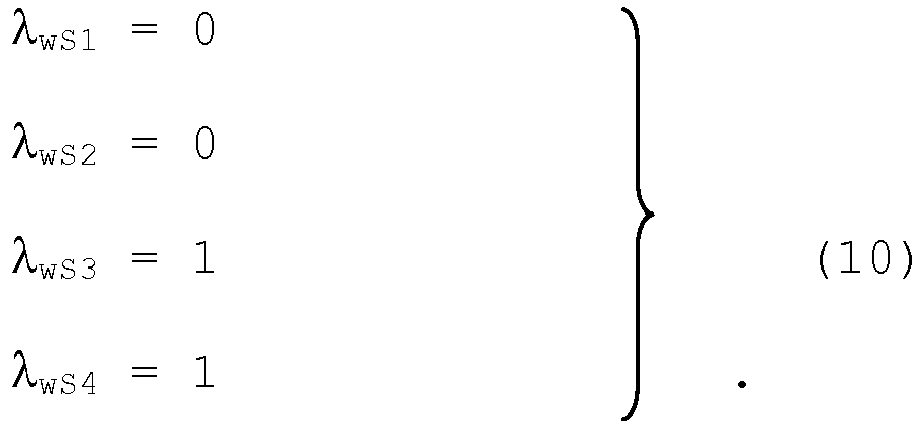
- In addition, in the
section 1, as is shown inFIGS. 8B and8C , the middle voltage command vmid* in the absolute middle value phase shifts from the voltage command vw0 in the W-phase to the voltage command vv0 in the V-phase with the polarities thereof being positive. Therefore, switching is carried out between the DC high voltage Ed and the DC middle voltage, i.e. zero voltage. For such switching, the respective on-time ratios λmidS1 to λmidS4 of the switching elements S1 to S4 in the DC circuit in each of the W-phase and the V-phase as the absolute middle value phase are expressed as the expressions (11):
- Furthermore, in the
section 1, as is also shown inFIGS. 8B and8C , the minimum voltage command vmin* in the absolute minimum value phase shifts from the voltage command vv0 in the V-phase to the voltage command vw0 in the W-phase with the polarities thereof being negative. Therefore, switching is carried out between the DC middle voltage, i.e. zero voltage and the DC low voltage -Ed. For such switching, the respective on-time ratios λminS1 to λminS4 of the switching elements S1 to S4 in the DC circuit in each of the V-phase and the W-phase as the absolute minimum value phase are expressed as the expressions (12):
- The on-time ratio operating means 30 shown in
FIG. 5 outputs the on-time ratios λmax*, λmid* and λmin* obtained from the inputted maximum voltage command vmax*, middle voltage command vmid* and minimum voltage command vmin*, respectively. - A by-phase on-time ratio operating means 40 converts the on-time ratios λmax*, λmid* and λmin* in each of the foregoing sections, which ratios are inputted to the
means 40 while being classified by value, into on-time ratios λu, λv and λw classified by phase of the U, V and W. As was explained in the foregoing, the on-time ratios λmid* and λmin* are proportional to the middle voltage command vmid* and the minimum voltage command vmin*, respectively, and the value of the on-time ratio λmax* is 1 or zero. Therefore, the waveforms of the on-time ratios λu, λv and λw are geometrically similar to the waveforms of the voltage commands vu0, vv0 and vw0 shown inFIGS. 8A ,8B and8C , respectively. However, the on-time ratios corresponding to the negative voltage commands become positive. - A triangular wave comparison means 50 as a carrier comparison means compares the waveforms of the on-time ratios λu, λv and λw in their respective U-, V- and W-phases with a triangular wave as a carrier to obtain on-off commands for the switching elements in the DC circuit of the inverter in each of the U-, V- and W-phases from the result of the comparison and outputs the obtained commands. Like in
FIG. 1 showing the configuration of the control system according to the first embodiment, signs Su1 to Sw4 designate on-off commands outputted from the triangular wave comparison means 50. Of the on-off commands Su1 to Sw4, the on-off commands Su1 to Su4 are the on-off commands to four switching elements (corresponding to the switching elements S1 to S4 shown inFIG. 14 ) in the DC circuit in the U-phase, the on-off commands Sv1 to Sv4 are the on-off commands to four switching elements in the DC circuit in the V-phase not shown, and the on-off commands Sw1 to Sw4 are the on-off commands to four switching elements in the DC circuit in the V-phase not shown. -
FIGURE 9 is a waveform diagram showing the operation of the triangular wave comparing means 50 according to the second embodiment in a part of thesection 1 with (a) showing the waveforms of the on-time ratios λu, λv, λw in the U-, V- and W-phases, respectively, together with the waveform of the triangular wave as a carrier, (b) showing the waveforms of the on-off commands Su1 to Su4 to the switching elements in the inverter in the U-phase, (c) showing the waveforms of the on-off commands Sv1 to Sv4 to the switching elements in the inverter in the V-phase, (d) showing the waveforms of the on-off commands Sw1 to Sw4 to the switching elements in the inverter in the W-phase. That is, (b), (c) and (d) ofFIG. 9 show the turned-on and -off states of the switching elements in the U-, V- and W-phases, respectively. Here, "a part of thesection 1" is the part from 0 to 0. 02 in thesection 1 when letting the length (time length) of thesection 1 shown inFIG. 6 to FIG. 8D be unity. In the following explanations, the reference signs of the on-off commands Su1 to Su4, Sv1 to Sv4 and Sw1 to Sw4 are to be also used as the reference signs of the switching elements. - Like in the first embodiment, by using an up-down counter, a carrier of a triangular wave is formed which moves between 0 and 1 as is shown in (a) of
FIG. 9 . The time length from the time at which the carrier initiates an increase from zero to the time at which the carrier returns to zero again after reaching 1 and then turning back therefrom becomes the one switching period. - Like in the first embodiment, the triangular wave comparison means 50 shown in
FIG. 5 is also formed by using a comparator contained in a device such as a microcomputer, with which means the values of the on-time ratios λu, λv and λw, corresponding to the values of the waveforms of the voltage commands vu0, vv0, vw0 in the U-, V- and W-phases shown inFIGS. 8A to 8C , respectively, are compared with the value of the triangular wave as a carrier as is shown in (a) ofFIG. 9 . The period of the triangular wave is equivalent to the one switching period of the switching element. - In the part of the
section 1 shown in (a) ofFIG. 9 , the on-time ratio λu is shown as the on-time ratio λmax* (=1) corresponding to the voltage command vu0 as the maximum voltage command vmax* (=1). The on-time ratio λv is shown as the on-time ratio λmin* corresponding to the voltage command vv0 as the minimum voltage command vmin* before the voltage command vv0 is shifted to the middle voltage command vmid*, and the on-time ratio λw is shown as the on-time ratio λmid* corresponding to the voltage command vw0 as the minimum voltage command vmid* before the voltage command vw0 is shifted to the minimum voltage command vmin*. Here, however, the on-time ratio λv as the on-time ratio λmin* corresponding to the voltage command vv0 being the negative minimum voltage command vmin*, is shown as being positive according to the expressions (8). - In addition, the part of the
section 1 shown inFIG. 9 is the part from 0 to 0.02 to the 1 as the length of thesection 1, i.e. a very short part of only 2% of thesection 1. Therefore, in such a short part, the waveform of the on-time ratio can be regarded as a straight line approximately representing a constant value and in parallel to the horizontal axis. - Like in the first embodiment, by the comparison between the value of the on-time ratio and the value of the carrier as the triangular wave, the time during which the value of the on-time ratio is equal to or more than the value of the carrier in the one switching period of the carrier, i.e. the one switching period of a switching element, is determined as the time during which the switching element is made turned-on with the on-time ratio by an on-off command.
- In this way, by using one carrier signal of a triangular wave, on-off commands, each having a determined on-time ratio, are formed with respect to each of the phases as is shown in (b), (c) and (d) of
FIG. 9 . - As is shown in (a) of
FIG. 9 , in thesection 1, the on-time ratio λu has the maximum value. Therefore, in (b) ofFIG. 9 , waveforms of the on-off commands Su1 to Su4, which are for carrying out switching of the switching elements Su1 to Su4 in the V-phase with the on-time ratios λuS1 to λuS4, respectively, being provided by the expressions (9), are shown in the part of thesection 1. - Namely, the on-time ratios λuS1 and λuS2 of the on-off commands Su1 and Su2 are left at 1 according to the expressions λuS1 = 1 and λuS2 = 1, respectively, which are provided by the expressions (9) and the on-time ratios λuS3 and λuS4 of the on-off commands Su3 and Su4 are left at 0 according to the expressions λuS3 = 0 and λuS4 = 0, respectively, which are provided by the expressions (9). This makes the switching elements Sui and Su2 left turned-on and the switching elements Su3 and Su4 left turned-off. In this way, in the U-phase, all of the switching elements Su1 to Su4 carry out no switching with the number of switching in the one switching period being zero.
- Here, in (b) of
FIG. 9 , the waveforms (characteristic lines) of the on-off commands Su1 and Su2 to their respective switching elements Su1 and Su2 coincide with each other and the waveforms (characteristic lines) of the on-off commands Su3 and Su4 to their respective switching elements Su3 and Su4 coincide with each other. - In (c) of
FIG. 9 , waveforms of the on-off commands Sv1 to Sv4, which are for carrying out switching of the switching elements Sv1 to Sv4 in the V-phase with the on-time ratios λmidS1 to λmidS4, respectively, being provided by the expressions (11), are shown in the part of thesection 1. - This makes each of the switching elements Sv1 and Sv3 carry out two times of switching, four times in total of both, in the one switching period.
- Compared with this, the on-time ratio λmidS2 of the on-off command Sv2 is left at 1 according to the expression λmidS2 = 1 provided by the expressions (11) and the on-time ratio λmidS4 of the on-off command Sv4 is left at 0 according to the expression λmidS4 = 0 provided by the expressions (11). That is, the switching elements Sv2 and Sv4 carry out no switching.
- In (d) of
FIG. 9 , waveforms of the on-off commands Sw1 to Sw4, which are for carrying out switching of the switching elements Sw1 to Sw4 in the W-phase with the on-time ratios λminS1 to λminS4, respectively, being provided by the expressions (12), are shown in the part of thesection 1. - This makes each of the switching elements Sw2 and Sw4 carry out two times of switching, four times in total of both, in the one switching period like the switching elements Su1 and Su3 in the U-phase.
- Compared with this, the on-time ratio λminS1 of the on-off command Sw1 is left at 0 according to the expression λminS1 = 0 provided by the expressions (12) and the on-time ratio λminS3 of the on-off command Sw3 is left at 1 according to the expression λminS3 = 1 provided by the expressions (12). That is, the switching elements Sw1 and Sw3 carry out no switching.
- By the switching operation like in the foregoing, a train of rectangular waves each with an on-time ratio changing with time, that is, a train of rectangular waves each with a width proportional to the value of the compensated voltage command changing with time, are formed with respect to each of three phases of the U-, V- and W-phases. The train of the rectangular waves are subjected to known demodulating processing to be converted into a three-level AC voltage.
- Therefore, also in the first embodiment, like in the first embodiment, the three-level inverter can be controlled by carrying out switching of eight times per switching period.
- Moreover, the carrier of the triangular wave can be easily produced to make it possible to form the control device at a low cost.
- Furthermore, in the second embodiment, no restriction is imposed on the amplitude of a voltage command, namely the value of a voltage that can be outputted from a three-level inverter.
-
FIGURE 10 is a waveform diagram showing the waveforms of the voltage commands vu0, vv0 and vw0 after the output voltage commands vu*, vv* and vw* shown inFIG. 2 are compensated with their respective amplitudes increased from illustrated 0.5 to 0.8 (letting the DC voltage be 1, from 50% to 80% to the DC voltage) in the first embodiment.FIGURE 11 is a waveform diagram showing the waveforms of voltage commands vu0, vv0 and vw0 after the compensation according to the second embodiment is carried out with respect to the output voltage commands vu*, vv* and vw* shown inFIG. 6 with their respective amplitudes similarly increased from illustrated 0.5 to 0.8. - As is apparent from
FIG. 10 , in the first embodiment, some parts of each of the voltage commands vu0, vv0 and vw0 are outside the range of -1 to 1, that is, outside the DC power supply voltage ranging from -Ed to Ed. Since the inverter cannot outputs a voltage with the absolute value thereof being larger than the power supply voltage Ed, the part of the voltage command with the value thereof exceeding 1 or -1 cannot produce voltages according to the command. This means that the output voltages are saturated to be distorted. This is because the compensation in the first embodiment is carried out so as to add a middle voltage command in the phase with the middle voltage command to a voltage commands in other phases as is expressed in the expressions (1) with the switching made stopped in the phase with the middle voltage command. That is, this is because in the phase with the maximum voltage command, an increased amplitude of the voltage command sometimes causes the value of the voltage command after the compensation to become larger than the value of the original maximum voltage command and exceed 1 by the addition. - Compared with this, in the second embodiment, with the value of the DC power supply voltage taken as 1, control is carried out so that the compensated value of the voltage command, the absolute value of which is maximum in each phase, becomes 1. Therefore, no voltage commands in the other phases exceed 1 to make it possible to output voltages while being limited to the value of the DC power supply voltage, by which there is no possibility of causing distortions in the output voltages.
- In the first embodiment, in a region in which the amplitude of the voltage command is small, the value of the zero-
phase voltage command 3w is smaller than that in the second embodiment, which provides the advantage of small potential variations in the zero-phase as a common mode that cause small noises. - Therefore, it is preferable to make use of the respective merits of the first embodiment and the second embodiment to distinguish between the use of the first embodiment and the use of the second embodiment according to the ratio of the amplitude of the voltage command to the DC power supply voltage.
- Namely, as is explained in the seventh aspect of the invention and shown in
FIG. 12 , an explanatory diagram showing the discrimination for switching between the control according to the first embodiment and the control according to the second embodiment, a discriminating means is provided for carrying out switching so that, with respect to the region in which the ratio of the amplitude as the maximum value of the voltage command to the DC power supply voltage is equal to or less than 0.6, the control of output voltages is carried out with the on-time ratios determined by the operations according to the first embodiment and, with respect to the region in which the ratio is more than 0.6, the control of output voltages is carried out with the on-time ratios determined by the operations according to the second embodiment. - The foregoing ratio 0.6 is a rough measure, which can be corrected with the voltage drops in the semiconductor switching elements and errors in detection circuits in detection circuits taken into consideration.
- The switching between control according to the first embodiment and the control according to the second embodiment switches the operation procedures of the voltage commands. Then, operations of the voltages commands according to both of the embodiments are not simultaneously carried out in parallel to cause no fear of increasing the burden of operational processing in a microcomputer. Furthermore, since the foregoing switching is carried out only by switching between voltage commands to be compared with the carrier, no shock due to pulses is generated at switching.
- While the present invention has been particularly shown and described with reference to the preferred embodiment thereof, it will be understood by those skilled in the art that the foregoing and other changes in form and details can be made therein without departing from the spirit and scope of the present invention.
Claims (8)
- A method for controlling a three-level inverter in a configuration in which three three-level inverters are connected in parallel to each other, the method comprising:the three three-level inverters carrying out turning-on and -off of a plurality of semiconductor switching elements, whereinat least one semiconductor switching element is connected between a high voltage point of a DC circuit and one output terminal,at least one semiconductor switching element is connected between a middle voltage point of the DC circuit and the output terminal, andat least one semiconductor switching element is connected between a low voltage point of the DC circuit and the output terminal, andenabling any one out of the three voltage levels of a DC high voltage, DC middle voltage, and DC low voltage as the base of an AC voltage for one phase to be outputted from the output terminal,the method makes a plurality of the semiconductor switching elements in each of the three three-level inverters turned-on and -off on the basis of output voltage commands of three-phase AC voltages to thereby make the three-phase AC voltage outputted,the method comprising the steps of:carrying out operations for obtaining on-time ratios of a plurality of the semiconductor switching elements in each of the three three-level inverters on the basis of the output voltage commands of the three-phase AC voltages;dividing the one period of the output voltage command of the three-phase AC voltage into a plurality of sections; andin each of the sections,making the three-level inverter for one phase alternately turn-on and-off the at least one semiconductor switching element connected between the high voltage point and the output terminal and the at least one semiconductor switching element connected between the middle voltage point and the output terminal with their respective operated on-time ratios in one switching period of the semiconductor switching element to alternately output the DC high voltage and the DC middle voltage;along with this, making the three-level inverter for one other phase fix the at least one switching element connected between the middle voltage point and the output terminal in a turned-on state to output the DC middle voltage; andalong with this, further making the three-level inverter for the remaining one phase alternately turn-on and -off the at least one semiconductor switching element connected between the middle voltage point and the output terminal and the at least one semiconductor switching element connected between the low voltage point and the output terminal with their respective operated on-time ratios in the one switching period to alternately output the DC middle voltage and the DC low voltage.
- The method for controlling a three-level inverter according to claim 1, further comprising the steps of:in each of the sections,with respect to a phase with the value of the output voltage command being a maximum value, carrying out compensation of subtracting a middle value of the output voltage command in another phase from the maximum value to provide thus compensated value as the value of a maximum voltage command in the phase in the section;with respect to the phase with the value of the output voltage command being the middle value, carrying out compensation of providing 0 as the value of a middle voltage command in the phase in the section;with respect to the rest phase with the value of the output voltage command being a minimum value, carrying out compensation of subtracting the middle value of the output voltage command from the minimum value to provide thus compensated value as the value of a minimum voltage command in the phase in the section;with respect to the phase with the value of the output voltage command being the minimum value, carrying out an operation of dividing the value of the maximum voltage command by the value of the DC high voltage to provide the on-time ratio of the at least one semiconductor switching element connected between the high voltage point and the output terminal in the three-level inverter in the phase and the on-time ratio of the at least one semiconductor switching element connected between the middle voltage point and the output terminal in the three-level inverter on the basis of the result of the division;with respect to the phase with the value of the output voltage commandbeing the middle value, carrying out an operation of providing 1 as the on-time ratio of fixing the at least one semiconductor switching element connected between the middle voltage point and the output terminal in the turned-on state in the three-level inverter in the phase on the basis of the value 0; andwith respect to the phase with the value of the output voltage command being the minimum value, carrying out an operation of dividing the value of the minimum voltage command by the value of the DC low voltage to provide the on-time ratio of the at least one semiconductor switching element connected between the middle voltage point and the output terminal in the three-level inverter in the phase and the on-time ratio of the at least one semiconductor switching element connected between the minimum voltage point and the output terminal in the three-level inverter on the basis of the result of the division.
- A system for controlling a three-level inverter for carrying out the method according to claim 1 or 2 comprising:a middle phase selecting means (20) configured for selecting, in each of the sections, an output voltage command of a phase with the value thereof being a middle value from the output voltage commands of the three-phase AC voltage;a maximum, middle and minimum voltage command operating means (10) configured for classifying, in each of the sections, the output voltage commands of the three-phase AC voltage by value into a voltage command of a phase with the value thereof being a maximum value, the selected voltage command of the phase with the value thereof being the middle value and a voltage command of a phase with the value thereof being a minimum value, and carrying out the compensation of subtracting the selected middle value from each of the classified output voltage commands to output the compensated results as a maximum voltage command, a middle voltage command with zero value and a minimum voltage command;an on-time ratio operating means (30) configured for carrying out, in each of the sections, an operation of dividing the value of the inputted maximum voltage command by the value of the DC high voltage to output the result of the operation as an operated value of the on-time ratio of the at least one semiconductor switching element connected between the high voltage point of the DC circuit and the one output terminal, carrying out an operation of converting the value 0 of the inputted middle voltage command into value 1 to output the value 1 as an operated value of the on-time ratio of fixing the at least one semiconductor switching element connected between the middle voltage point of the DC circuit and the one output terminal in the turned-on state, and carrying out an operation of dividing the value of the inputted minimum voltage command by the value of the DC low voltage to output the result of the operation as an operated value of the on-time ratio of the at least one semiconductor switching element connected between the low voltage point of the DC circuit and the one output terminal;a by-phase on-time ratio operating means (40) configured for classifying by phase, in each of the sections, the operated values of the on-time ratios, which are classified by values, and outputting the operated values classified by phase as voltages with the values thereof corresponding to the on-time ratios; anda carrier comparing means (50) configured for making, in each of the sections, the voltages, inputted by phase with the values thereof corresponding to the on-time ratios, compared with a carrier, which converts the compared voltage into an on-off command with an on-time ratio corresponding to the compared voltage, to produce on-off commands with the on-time ratios by phase and provide the on-off commands as those for a plurality of the semiconductor switching elements in each of the three three-level inverters.
- A method for controlling a three-level inverter in a configuration in which three three-level inverters are connected in parallel to each other, the method comprising
the three three-level inverters carrying out turning-on and -off of a plurality of semiconductor switching elements, wherein
at least one semiconductor switching element is connected between a high voltage point of a DC circuit and one output terminal,
at least one semiconductor switching element is connected between a middle voltage point of the DC circuit and the output terminal, and
at least one semiconductor switching element is connected between a low voltage point of the DC circuit and the output terminal, and
enabling any one out of three voltage levels of a DC high voltage, DC middle voltage and DC low voltage as the base of an AC voltage for one phase to be outputted from the output terminal,
the method makes a plurality of the semiconductor switching elements in each of the three three-level inverters turned-on and -off on the basis of output voltage commands of three-phase AC voltages to thereby make the three-phase AC voltage outputted,
the method comprising the steps of:carrying out operations for obtaining on-time ratios of a plurality of the semiconductor switching elements in each of the three three-level inverters on the basis of the output voltage commands of the three-phase AC voltages;dividing the one period of the output voltage command of the three-phase AC voltage into a plurality of sections; andin each of the sections,making the three-level inverter for one phase fix one of the at least one semiconductor switching element connected between the high voltage point and the output terminal and the at least one semiconductor switching element connected between the low voltage point and the output terminal in a turned-on state to output one of the DC high voltage and the DC low voltage;along with this, making the three-level inverter for one other phase alternately turn-on and -off one of the at least one semiconductor switching element connected between the high voltage point and the output terminal and the at least one semiconductor switching element connected between the low voltage point and the output terminal with the at least one semiconductor switching element connected between the middle voltage point and the output terminal with their respective operated on-time ratios in one switching period of the semiconductor switching element to alternately output one of the DC high voltage and the DC low voltage with the DC middle voltage; andalong with this, when making the three-level inverter for the remaining one phase output the DC high voltage, further making the three-level inverter for the remaining one phase alternately turn-on and -off the at least one semiconductor switching element connected between the low voltage point and the output terminal and the at least one semiconductor switching element connected between the middle voltage point and the output terminal with their respective operated on-time ratios in one switching period of the semiconductor switching element to alternately output the DC low voltage with the DC middle voltage; andwhen making the three-level inverter for the one other phase output the DC low voltage, further making the three-level inverter for the remaining one phase alternately turn-on and -off the at least one semiconductor switching element connected between the high voltage point and the output terminal and the at least one semiconductor switching element connected between the middle voltage point and the output terminal with their respective operated on-time ratios in one switching period of the semiconductor switching element to alternately output the DC high voltage with the DC middle voltage. - The method for controlling a three-level inverter according to claim 4 comprising the steps of:in each of the sections,when the output voltage command has the positive polarity and the absolute value of the maximum value,with respect to a phase with the output voltage command having the positive polarity and the absolute value of the maximum value,making the value of the DC high voltage as the maximum value of the compensated voltage command, providing the value of the DC high voltage as the maximum voltage command in the phase in the section, carrying out an operation of dividing the maximum voltage command by the value of the DC high voltage and, on the basis of the result of the division, providing 1 as the on-time ratio of fixing the at least one semiconductor switching element connected between the low voltage point and the output terminal in the turned-on state in the three-level inverter in the phase;with respect to a phase with the value of the output voltage command being a middle value,carrying out compensation of adding the difference between the value of the DC high voltage and the maximum value of the output voltage command to the middle value of the voltage command, providing the value of the compensated voltage command as the value of the middle voltage command in the phase in the section, carrying out an operation of dividing the value of the middle voltage command by the value of the DC high voltage and, on the basis of the result of the division and the polarity of the middle voltage command, providing the on-time ratio of one of the at least one semiconductor switching element connected between the high voltage point and the output terminal in the three-level inverter in the phase and the at least one semiconductor switching element connected between the low voltage point and the output terminal in the inverter in the phase and the on-time ratio of the at least one semiconductor switching element connected between the middle voltage point and the output terminal in the inverter in the phase;with respect to a phase with the value of the output voltage command being a minimum value,carrying out compensation of adding the difference between the value of the DC high voltage and the maximum value of the output voltage command to the minimum value of the voltage command, providing the value of the compensated voltage command as the value of the minimum voltage command in the phase in the section, carrying out an operation of dividing the value of the minimum voltage command by the value of the DC high voltage and, on the basis of the result of the division and the polarity of the minimum voltage command, providing the on-time ratio of one of the at least one semiconductor switching element connected between the high voltage point and the output terminal in the three-level inverter in the phase and the at least one semiconductor switching element connected between the high voltage point and the output terminal in the inverter in the phase and the on-time ratio of the at least one semiconductor switching element connected between the minimum voltage point and the output terminal in the inverter in the phase;when the output voltage command has the negative polarity and the absolute value of the maximum value,with respect to a phase with the output voltage command having the negative polarity and the absolute value of the maximum value,making the absolute value of the DC low voltage as the maximum value of the compensated voltage command, providing the absolute value of the DC low voltage as the maximum voltage command in the phase in the section, carrying out an operation of dividing the absolute value of the maximum voltage command by the absolute value of the DC low voltage and, on the basis of the result of the division, providing 1 as the on-time ratio of fixing the at least one semiconductor switching element connected between the low voltage point and the output terminal in the turned-on state in the three-level inverter in the phase;with respect to a phase with the value of the output voltage command being a middle value,carrying out compensation of subtracting the difference between the absolute value of the DC low voltage and the maximum value of the output voltage command from the middle value of the voltage command, providing the value of the compensated voltage command as the value of the middle voltage command in the phase in the section, carrying out an operation of dividing the value of the middle voltage command by the absolute value of the DC low voltage and, on the basis of the result of the division and the polarity of the middle voltage command, providing the on-time ratio of one of the at least one semiconductor switching element connected between the high voltage point and the output terminal in the three-level inverter in the phase and the at least one semiconductor switching element connected between the low voltage point and the output terminal in the inverter in the phase and the on-time ratio of the at least one semiconductor switching element connected between the middle voltage point and the output terminal in the inverter in the phase; andwith respect to a phase with the value of the output voltage command being a minimum value,carrying out compensation of subtracting the difference between the absolute value of the DC low voltage and the maximum value of the output voltage command to the minimum value of the voltage command, providing the value of the compensated voltage command as the value of the minimum voltage command in the phase in the section, carrying out an operation of dividing the value of the minimum voltage command by the absolute value of the DC low voltage and, on the basis of the result of the division and the polarity of the middle voltage command, providing the on-time ratio of one of the at least one semiconductor switching element connected between the high voltage point and the output terminal in the three-level inverter in the phase and the at least one semiconductor switching element connected between the low voltage point and the output terminal in the inverter in the phase and the on-time ratio of the at least one semiconductor switching element connected between the minimum voltage point and the output terminal.
- A system for controlling a three-level inverter for carrying out the method according to claim 4 or 5 comprising:an absolute maximum value command discriminating means (70) configured for detecting, in each of the sections, an output voltage command of a phase with an absolute value of the maximum value from the output voltage commands of the three-phase AC voltage and carrying out an operation for providing a compensation value for the output voltage commands on the basis of the maximum value and the polarity thereof;a maximum, middle and minimum voltage command operating means (10) configured for classifying, in each of the sections, the output voltage commands of the three-phase AC voltage by value into a voltage command of a phase with the value thereof being a maximum value, a voltage command of the phase with the value thereof being the middle value and a voltage command of a phase with the value thereof being a minimum value, carrying out the compensation of adding the compensation value when the polarity of the maximum value is positive and subtracting the compensation value when the polarity of the maximum value is negative, and outputting the compensated results as a maximum voltage command with the value thereof being one of the value of the DC high voltage and the absolute value of the DC low voltage, a middle voltage command and a minimum voltage command;an on-time ratio operating means (30) configured for carrying out, in each of the sections, an operation of dividing the value of the inputted maximum voltage command by the value of one of the value of the DC high voltage and the absolute value of the DC low voltage on the basis of the polarity of the maximum value to convert the value of the inputted maximum voltage command to 1 to output the result of the operation as an operated value of the on-time ratio of fixing the at least one semiconductor switching element connected between one of the high voltage point and the low voltage point and the one output terminal in the turned-on state, carrying out an operation of dividing the value of the inputted middle voltage command by one of the value of the DC high voltage and the absolute value of the DC low voltage on the basis of the polarity of the maximum value to output the result of the operation as an operated value of the on-time ratio of the at least one semiconductor switching element connected between one of the high voltage point and the low voltage point of the DC circuit and the one output terminal, and carrying out an operation of dividing the value of the inputted minimum voltage command by one of the value of the DC high voltage and the absolute value of the DC low voltage on the basis of the polarity of the maximum value to output the result of the operation as an operated value of the on-time ratio of the at least one semiconductor switching element connected between one of the high voltage point and the low voltage point of the DC circuit and the one output terminal;a by-phase on-time ratio operating means (40) configured for classifying by phase, in each of the sections, the operated values of the on-time ratios, which are classified by values, and outputting the operated values classified by phase as voltages with the values thereof corresponding to the on-time ratios; anda carrier comparing means (50) configured for making, in each of the sections, the voltages, inputted by phase with the values thereof corresponding to the on-time ratios, compared with a carrier, which converts the compared voltage into an on-off command with an on-time ratio corresponding to the compared voltage, to produce on-off commands with the on-time ratios by phase and provide the on-off commands as those for a plurality of the semiconductor switching elements in each of the three three-level inverters.
- The control method of a three-level inverter carried out as the method according to claim 1 or 2 when the amplitude of a three-phase output voltage command is equal to or less than a specified value and carried out as the method according to claim 4 or 5 when the amplitude of the three-phase output voltage command is equal to or more than the specified value.
- The system for controlling a three-level inverter according to claim 3 or 6, wherein the carrier is a triangular wave.
Applications Claiming Priority (1)
| Application Number | Priority Date | Filing Date | Title |
|---|---|---|---|
| JP2014166375A JP6176495B2 (en) | 2014-08-19 | 2014-08-19 | 3-level inverter control method and control apparatus |
Publications (3)
| Publication Number | Publication Date |
|---|---|
| EP2988407A2 true EP2988407A2 (en) | 2016-02-24 |
| EP2988407A3 EP2988407A3 (en) | 2016-11-02 |
| EP2988407B1 EP2988407B1 (en) | 2020-04-29 |
Family
ID=53794097
Family Applications (1)
| Application Number | Title | Priority Date | Filing Date |
|---|---|---|---|
| EP15180324.4A Active EP2988407B1 (en) | 2014-08-19 | 2015-08-10 | Control method and control system of three level inverter |
Country Status (3)
| Country | Link |
|---|---|
| US (1) | US9520805B2 (en) |
| EP (1) | EP2988407B1 (en) |
| JP (1) | JP6176495B2 (en) |
Families Citing this family (6)
| Publication number | Priority date | Publication date | Assignee | Title |
|---|---|---|---|---|
| CN108123639B (en) * | 2016-11-30 | 2020-02-21 | 华为技术有限公司 | Pulse width modulation method, pulse width modulation system and controller |
| CN106533236B (en) * | 2016-12-15 | 2018-10-16 | 电子科技大学 | A kind of minimum switch losses implementation method of three-level inverter |
| JP6361803B1 (en) * | 2017-07-27 | 2018-07-25 | 株式会社明電舎 | Multilevel inverter control device and control method |
| US10536094B2 (en) * | 2017-11-20 | 2020-01-14 | Solaredge Technologies Ltd. | Efficient switching for converter circuit |
| DE112020006987T5 (en) | 2020-03-27 | 2023-01-12 | Mitsubishi Electric Corporation | Three-level power converter and method for controlling an intermediate potential of a DC power supply unit |
| CN112968624A (en) * | 2021-03-17 | 2021-06-15 | 山特电子(深圳)有限公司 | Bidirectional DC-AC conversion circuit and starting method thereof |
Citations (2)
| Publication number | Priority date | Publication date | Assignee | Title |
|---|---|---|---|---|
| JP2007282484A (en) | 2007-03-26 | 2007-10-25 | Hitachi Ltd | 3-level power converter |
| JP2010206931A (en) | 2009-03-03 | 2010-09-16 | Fuji Electric Systems Co Ltd | Method and device for control of three-level inverter |
Family Cites Families (32)
| Publication number | Priority date | Publication date | Assignee | Title |
|---|---|---|---|---|
| US5517401A (en) * | 1992-02-07 | 1996-05-14 | Fuji Electric Co., Ltd. | Three level pulse width modulated inverter for an electric vehicle |
| US6697271B2 (en) * | 2000-08-16 | 2004-02-24 | Northrop Grumman Corporation | Cascaded multi-level H-bridge drive |
| US6337804B1 (en) * | 2000-09-26 | 2002-01-08 | General Electric Company | Multilevel PWM voltage source inverter control at low output frequencies |
| CN100334801C (en) * | 2000-12-07 | 2007-08-29 | 株式会社安川电机 | Neutral Point Clamped Pulse Width Modulation Inverter Device |
| MXPA05001099A (en) * | 2002-07-31 | 2005-09-08 | Smc Electrical Products Inc | Low voltage, two-level, six-pulse induction motor controller driving a medium-to-high voltage, three-or-more-level ac drive inverter bridge. |
| US7426122B2 (en) * | 2003-08-25 | 2008-09-16 | Mitsubishi Denki Kabushiki Kaisha | Power-converter control apparatus employing pulse width modulation and adjusting duration of a zero-voltage vector |
| US7050311B2 (en) * | 2003-11-25 | 2006-05-23 | Electric Power Research Institute, Inc. | Multilevel converter based intelligent universal transformer |
| JP4274023B2 (en) * | 2004-03-31 | 2009-06-03 | 株式会社安川電機 | PWM cycloconverter control method and control apparatus |
| US8581147B2 (en) * | 2005-03-24 | 2013-11-12 | Lincoln Global, Inc. | Three stage power source for electric ARC welding |
| JP5099305B2 (en) * | 2006-07-31 | 2012-12-19 | 富士電機株式会社 | Control device for direct power converter |
| US7573732B2 (en) * | 2007-05-25 | 2009-08-11 | General Electric Company | Protective circuit and method for multi-level converter |
| JP5474772B2 (en) * | 2007-06-01 | 2014-04-16 | ディーアールエス パワー アンド コントロール テクノロジーズ インコーポレーテッド | Three-level neutral point fixed conversion device and control method thereof |
| FR2942088B1 (en) * | 2009-02-11 | 2011-03-11 | Converteam Technology Ltd | VOLTAGE INVERTER WITH 3N-4 LEVELS |
| US8498137B2 (en) * | 2009-12-11 | 2013-07-30 | Magna International, Inc. | Boost multilevel inverter system |
| DE102010008426B4 (en) * | 2010-02-18 | 2011-09-01 | Hochschule Konstanz | 3-stage pulse inverter with discharge network |
| JP2012044824A (en) * | 2010-08-23 | 2012-03-01 | Fuji Electric Co Ltd | Power conversion device |
| JP5734609B2 (en) * | 2010-09-22 | 2015-06-17 | 株式会社ダイヘン | Inverter device and grid-connected inverter system provided with this inverter device |
| JP5163734B2 (en) * | 2010-12-17 | 2013-03-13 | 富士電機株式会社 | 3-level inverter |
| JP5753742B2 (en) * | 2011-07-14 | 2015-07-22 | 株式会社ダイヘン | Inverter device and grid-connected inverter system provided with this inverter device |
| JP5865657B2 (en) * | 2011-03-24 | 2016-02-17 | 株式会社ダイヘン | Control circuit for controlling power conversion circuit, grid-connected inverter system provided with this control circuit |
| JP5726055B2 (en) * | 2011-12-01 | 2015-05-27 | 三菱電機株式会社 | Power converter |
| AU2012364265B2 (en) * | 2012-01-05 | 2017-05-18 | Schneider Electric It Corporation | Methods and apparatus for controlling power switches via a digital communication bus |
| US9425622B2 (en) * | 2013-01-08 | 2016-08-23 | Infineon Technologies Austria Ag | Power converter circuit with AC output and at least one transformer |
| JP5370519B2 (en) | 2012-03-15 | 2013-12-18 | 富士電機株式会社 | Power converter |
| JP6040582B2 (en) * | 2012-06-14 | 2016-12-07 | 富士電機株式会社 | Protection control method for multi-level power conversion circuit |
| EP2913915B1 (en) * | 2012-10-23 | 2018-08-01 | Mitsubishi Electric Corporation | Power conversion device |
| EP2919377B1 (en) * | 2012-11-09 | 2018-10-31 | Fuji Electric Co., Ltd. | Inverter device |
| US9252670B2 (en) * | 2012-12-19 | 2016-02-02 | General Electric Company | Multilevel converter |
| KR101791289B1 (en) * | 2013-06-17 | 2017-10-27 | 엘에스산전 주식회사 | Multi-level inverter |
| US20150015072A1 (en) * | 2013-07-12 | 2015-01-15 | Infineon Technologies Austria Ag | Power Converter Circuit and Method |
| US9148071B2 (en) * | 2013-07-29 | 2015-09-29 | Rhombus Energy Solutions, Inc. | DC source-to-AC grid tie-in power enhancement using multilevel inverter topology and resonant matrix tank converter |
| US20150092467A1 (en) * | 2013-09-30 | 2015-04-02 | Infineon Technologies Ag | Driver Circuit for a Pair of Semiconductor Switches in a Leg of a Three-Level Inverter Half-Bridge |
-
2014
- 2014-08-19 JP JP2014166375A patent/JP6176495B2/en active Active
-
2015
- 2015-08-10 EP EP15180324.4A patent/EP2988407B1/en active Active
- 2015-08-12 US US14/824,454 patent/US9520805B2/en active Active
Patent Citations (2)
| Publication number | Priority date | Publication date | Assignee | Title |
|---|---|---|---|---|
| JP2007282484A (en) | 2007-03-26 | 2007-10-25 | Hitachi Ltd | 3-level power converter |
| JP2010206931A (en) | 2009-03-03 | 2010-09-16 | Fuji Electric Systems Co Ltd | Method and device for control of three-level inverter |
Also Published As
| Publication number | Publication date |
|---|---|
| JP2016042772A (en) | 2016-03-31 |
| EP2988407B1 (en) | 2020-04-29 |
| JP6176495B2 (en) | 2017-08-09 |
| EP2988407A3 (en) | 2016-11-02 |
| US9520805B2 (en) | 2016-12-13 |
| US20160072406A1 (en) | 2016-03-10 |
Similar Documents
| Publication | Publication Date | Title |
|---|---|---|
| EP2988407B1 (en) | Control method and control system of three level inverter | |
| EP2894780B1 (en) | Multilevel converter systems and methods with reduced common mode voltage | |
| JP2685586B2 (en) | Multiple inverter device | |
| US5159539A (en) | High frequency DC/AC power converting apparatus | |
| US9660482B2 (en) | Power conversion device with momentary voltage drop compensation | |
| EP4586490A1 (en) | Multi-level inverter | |
| EP1411624B1 (en) | Power inverter | |
| JP5205094B2 (en) | Inverter control device | |
| JP3856689B2 (en) | Neutral point clamp type power converter controller | |
| CN104682761A (en) | Current source power conversion apparatus | |
| JP6208089B2 (en) | Three-level three-phase inverter drive controller | |
| JP4873317B2 (en) | Inverter device | |
| US11863098B2 (en) | Multi-level inverter | |
| US9685884B2 (en) | Seven-level inverter apparatus | |
| US20250219551A1 (en) | Power conversion device | |
| WO2019049698A1 (en) | Power conversion circuit and power conversion device | |
| JPH09182452A (en) | Three-level inverter device | |
| JP5025331B2 (en) | PWM control method and power converter using the same | |
| JP4951388B2 (en) | Power converter | |
| JP7494321B2 (en) | Three-phase three-level inverter drive control device and drive control method | |
| CN105391308A (en) | Matrix converter, matrix converter control device and matrix converter control method | |
| JP6361803B1 (en) | Multilevel inverter control device and control method | |
| EP4266567A1 (en) | Power conversion device | |
| JP6769526B1 (en) | Inverter system and control method of inverter system | |
| JP6575865B2 (en) | 3-level inverter control method and control apparatus |
Legal Events
| Date | Code | Title | Description |
|---|---|---|---|
| PUAI | Public reference made under article 153(3) epc to a published international application that has entered the european phase |
Free format text: ORIGINAL CODE: 0009012 |
|
| AK | Designated contracting states |
Kind code of ref document: A2 Designated state(s): AL AT BE BG CH CY CZ DE DK EE ES FI FR GB GR HR HU IE IS IT LI LT LU LV MC MK MT NL NO PL PT RO RS SE SI SK SM TR |
|
| AX | Request for extension of the european patent |
Extension state: BA ME |
|
| PUAL | Search report despatched |
Free format text: ORIGINAL CODE: 0009013 |
|
| AK | Designated contracting states |
Kind code of ref document: A3 Designated state(s): AL AT BE BG CH CY CZ DE DK EE ES FI FR GB GR HR HU IE IS IT LI LT LU LV MC MK MT NL NO PL PT RO RS SE SI SK SM TR |
|
| AX | Request for extension of the european patent |
Extension state: BA ME |
|
| RIC1 | Information provided on ipc code assigned before grant |
Ipc: H02M 7/487 20070101ALI20160928BHEP Ipc: H02M 7/483 20070101AFI20160928BHEP Ipc: H02M 7/537 20060101ALI20160928BHEP Ipc: H02M 1/00 20060101ALI20160928BHEP |
|
| 17P | Request for examination filed |
Effective date: 20170502 |
|
| RBV | Designated contracting states (corrected) |
Designated state(s): AL AT BE BG CH CY CZ DE DK EE ES FI FR GB GR HR HU IE IS IT LI LT LU LV MC MK MT NL NO PL PT RO RS SE SI SK SM TR |
|
| STAA | Information on the status of an ep patent application or granted ep patent |
Free format text: STATUS: REQUEST FOR EXAMINATION WAS MADE |
|
| STAA | Information on the status of an ep patent application or granted ep patent |
Free format text: STATUS: EXAMINATION IS IN PROGRESS |
|
| 17Q | First examination report despatched |
Effective date: 20180604 |
|
| GRAP | Despatch of communication of intention to grant a patent |
Free format text: ORIGINAL CODE: EPIDOSNIGR1 |
|
| STAA | Information on the status of an ep patent application or granted ep patent |
Free format text: STATUS: GRANT OF PATENT IS INTENDED |
|
| INTG | Intention to grant announced |
Effective date: 20191108 |
|
| GRAS | Grant fee paid |
Free format text: ORIGINAL CODE: EPIDOSNIGR3 |
|
| GRAA | (expected) grant |
Free format text: ORIGINAL CODE: 0009210 |
|
| STAA | Information on the status of an ep patent application or granted ep patent |
Free format text: STATUS: THE PATENT HAS BEEN GRANTED |
|
| AK | Designated contracting states |
Kind code of ref document: B1 Designated state(s): AL AT BE BG CH CY CZ DE DK EE ES FI FR GB GR HR HU IE IS IT LI LT LU LV MC MK MT NL NO PL PT RO RS SE SI SK SM TR |
|
| REG | Reference to a national code |
Ref country code: GB Ref legal event code: FG4D |
|
| REG | Reference to a national code |
Ref country code: CH Ref legal event code: EP |
|
| REG | Reference to a national code |
Ref country code: AT Ref legal event code: REF Ref document number: 1264819 Country of ref document: AT Kind code of ref document: T Effective date: 20200515 |
|
| REG | Reference to a national code |
Ref country code: DE Ref legal event code: R096 Ref document number: 602015051511 Country of ref document: DE |
|
| REG | Reference to a national code |
Ref country code: IE Ref legal event code: FG4D |
|
| REG | Reference to a national code |
Ref country code: NL Ref legal event code: MP Effective date: 20200429 |
|
| REG | Reference to a national code |
Ref country code: LT Ref legal event code: MG4D |
|
| PG25 | Lapsed in a contracting state [announced via postgrant information from national office to epo] |
Ref country code: LT Free format text: LAPSE BECAUSE OF FAILURE TO SUBMIT A TRANSLATION OF THE DESCRIPTION OR TO PAY THE FEE WITHIN THE PRESCRIBED TIME-LIMIT Effective date: 20200429 Ref country code: NO Free format text: LAPSE BECAUSE OF FAILURE TO SUBMIT A TRANSLATION OF THE DESCRIPTION OR TO PAY THE FEE WITHIN THE PRESCRIBED TIME-LIMIT Effective date: 20200729 Ref country code: FI Free format text: LAPSE BECAUSE OF FAILURE TO SUBMIT A TRANSLATION OF THE DESCRIPTION OR TO PAY THE FEE WITHIN THE PRESCRIBED TIME-LIMIT Effective date: 20200429 Ref country code: SE Free format text: LAPSE BECAUSE OF FAILURE TO SUBMIT A TRANSLATION OF THE DESCRIPTION OR TO PAY THE FEE WITHIN THE PRESCRIBED TIME-LIMIT Effective date: 20200429 Ref country code: IS Free format text: LAPSE BECAUSE OF FAILURE TO SUBMIT A TRANSLATION OF THE DESCRIPTION OR TO PAY THE FEE WITHIN THE PRESCRIBED TIME-LIMIT Effective date: 20200829 Ref country code: GR Free format text: LAPSE BECAUSE OF FAILURE TO SUBMIT A TRANSLATION OF THE DESCRIPTION OR TO PAY THE FEE WITHIN THE PRESCRIBED TIME-LIMIT Effective date: 20200730 Ref country code: PT Free format text: LAPSE BECAUSE OF FAILURE TO SUBMIT A TRANSLATION OF THE DESCRIPTION OR TO PAY THE FEE WITHIN THE PRESCRIBED TIME-LIMIT Effective date: 20200831 |
|
| REG | Reference to a national code |
Ref country code: AT Ref legal event code: MK05 Ref document number: 1264819 Country of ref document: AT Kind code of ref document: T Effective date: 20200429 |
|
| PG25 | Lapsed in a contracting state [announced via postgrant information from national office to epo] |
Ref country code: HR Free format text: LAPSE BECAUSE OF FAILURE TO SUBMIT A TRANSLATION OF THE DESCRIPTION OR TO PAY THE FEE WITHIN THE PRESCRIBED TIME-LIMIT Effective date: 20200429 Ref country code: RS Free format text: LAPSE BECAUSE OF FAILURE TO SUBMIT A TRANSLATION OF THE DESCRIPTION OR TO PAY THE FEE WITHIN THE PRESCRIBED TIME-LIMIT Effective date: 20200429 Ref country code: LV Free format text: LAPSE BECAUSE OF FAILURE TO SUBMIT A TRANSLATION OF THE DESCRIPTION OR TO PAY THE FEE WITHIN THE PRESCRIBED TIME-LIMIT Effective date: 20200429 Ref country code: BG Free format text: LAPSE BECAUSE OF FAILURE TO SUBMIT A TRANSLATION OF THE DESCRIPTION OR TO PAY THE FEE WITHIN THE PRESCRIBED TIME-LIMIT Effective date: 20200729 |
|
| PG25 | Lapsed in a contracting state [announced via postgrant information from national office to epo] |
Ref country code: AL Free format text: LAPSE BECAUSE OF FAILURE TO SUBMIT A TRANSLATION OF THE DESCRIPTION OR TO PAY THE FEE WITHIN THE PRESCRIBED TIME-LIMIT Effective date: 20200429 Ref country code: NL Free format text: LAPSE BECAUSE OF FAILURE TO SUBMIT A TRANSLATION OF THE DESCRIPTION OR TO PAY THE FEE WITHIN THE PRESCRIBED TIME-LIMIT Effective date: 20200429 |
|
| PG25 | Lapsed in a contracting state [announced via postgrant information from national office to epo] |
Ref country code: ES Free format text: LAPSE BECAUSE OF FAILURE TO SUBMIT A TRANSLATION OF THE DESCRIPTION OR TO PAY THE FEE WITHIN THE PRESCRIBED TIME-LIMIT Effective date: 20200429 Ref country code: CZ Free format text: LAPSE BECAUSE OF FAILURE TO SUBMIT A TRANSLATION OF THE DESCRIPTION OR TO PAY THE FEE WITHIN THE PRESCRIBED TIME-LIMIT Effective date: 20200429 Ref country code: SM Free format text: LAPSE BECAUSE OF FAILURE TO SUBMIT A TRANSLATION OF THE DESCRIPTION OR TO PAY THE FEE WITHIN THE PRESCRIBED TIME-LIMIT Effective date: 20200429 Ref country code: RO Free format text: LAPSE BECAUSE OF FAILURE TO SUBMIT A TRANSLATION OF THE DESCRIPTION OR TO PAY THE FEE WITHIN THE PRESCRIBED TIME-LIMIT Effective date: 20200429 Ref country code: IT Free format text: LAPSE BECAUSE OF FAILURE TO SUBMIT A TRANSLATION OF THE DESCRIPTION OR TO PAY THE FEE WITHIN THE PRESCRIBED TIME-LIMIT Effective date: 20200429 Ref country code: DK Free format text: LAPSE BECAUSE OF FAILURE TO SUBMIT A TRANSLATION OF THE DESCRIPTION OR TO PAY THE FEE WITHIN THE PRESCRIBED TIME-LIMIT Effective date: 20200429 Ref country code: EE Free format text: LAPSE BECAUSE OF FAILURE TO SUBMIT A TRANSLATION OF THE DESCRIPTION OR TO PAY THE FEE WITHIN THE PRESCRIBED TIME-LIMIT Effective date: 20200429 Ref country code: AT Free format text: LAPSE BECAUSE OF FAILURE TO SUBMIT A TRANSLATION OF THE DESCRIPTION OR TO PAY THE FEE WITHIN THE PRESCRIBED TIME-LIMIT Effective date: 20200429 |
|
| REG | Reference to a national code |
Ref country code: DE Ref legal event code: R097 Ref document number: 602015051511 Country of ref document: DE |
|
| PG25 | Lapsed in a contracting state [announced via postgrant information from national office to epo] |
Ref country code: PL Free format text: LAPSE BECAUSE OF FAILURE TO SUBMIT A TRANSLATION OF THE DESCRIPTION OR TO PAY THE FEE WITHIN THE PRESCRIBED TIME-LIMIT Effective date: 20200429 Ref country code: SK Free format text: LAPSE BECAUSE OF FAILURE TO SUBMIT A TRANSLATION OF THE DESCRIPTION OR TO PAY THE FEE WITHIN THE PRESCRIBED TIME-LIMIT Effective date: 20200429 |
|
| PLBE | No opposition filed within time limit |
Free format text: ORIGINAL CODE: 0009261 |
|
| STAA | Information on the status of an ep patent application or granted ep patent |
Free format text: STATUS: NO OPPOSITION FILED WITHIN TIME LIMIT |
|
| PG25 | Lapsed in a contracting state [announced via postgrant information from national office to epo] |
Ref country code: MC Free format text: LAPSE BECAUSE OF FAILURE TO SUBMIT A TRANSLATION OF THE DESCRIPTION OR TO PAY THE FEE WITHIN THE PRESCRIBED TIME-LIMIT Effective date: 20200429 |
|
| REG | Reference to a national code |
Ref country code: CH Ref legal event code: PL |
|
| 26N | No opposition filed |
Effective date: 20210201 |
|
| GBPC | Gb: european patent ceased through non-payment of renewal fee |
Effective date: 20200810 |
|
| PG25 | Lapsed in a contracting state [announced via postgrant information from national office to epo] |
Ref country code: CH Free format text: LAPSE BECAUSE OF NON-PAYMENT OF DUE FEES Effective date: 20200831 Ref country code: LI Free format text: LAPSE BECAUSE OF NON-PAYMENT OF DUE FEES Effective date: 20200831 Ref country code: LU Free format text: LAPSE BECAUSE OF NON-PAYMENT OF DUE FEES Effective date: 20200810 |
|
| REG | Reference to a national code |
Ref country code: BE Ref legal event code: MM Effective date: 20200831 |
|
| PG25 | Lapsed in a contracting state [announced via postgrant information from national office to epo] |
Ref country code: SI Free format text: LAPSE BECAUSE OF FAILURE TO SUBMIT A TRANSLATION OF THE DESCRIPTION OR TO PAY THE FEE WITHIN THE PRESCRIBED TIME-LIMIT Effective date: 20200429 |
|
| PG25 | Lapsed in a contracting state [announced via postgrant information from national office to epo] |
Ref country code: FR Free format text: LAPSE BECAUSE OF NON-PAYMENT OF DUE FEES Effective date: 20200831 |
|
| PG25 | Lapsed in a contracting state [announced via postgrant information from national office to epo] |
Ref country code: GB Free format text: LAPSE BECAUSE OF NON-PAYMENT OF DUE FEES Effective date: 20200810 Ref country code: IE Free format text: LAPSE BECAUSE OF NON-PAYMENT OF DUE FEES Effective date: 20200810 Ref country code: BE Free format text: LAPSE BECAUSE OF NON-PAYMENT OF DUE FEES Effective date: 20200831 |
|
| PG25 | Lapsed in a contracting state [announced via postgrant information from national office to epo] |
Ref country code: TR Free format text: LAPSE BECAUSE OF FAILURE TO SUBMIT A TRANSLATION OF THE DESCRIPTION OR TO PAY THE FEE WITHIN THE PRESCRIBED TIME-LIMIT Effective date: 20200429 Ref country code: MT Free format text: LAPSE BECAUSE OF FAILURE TO SUBMIT A TRANSLATION OF THE DESCRIPTION OR TO PAY THE FEE WITHIN THE PRESCRIBED TIME-LIMIT Effective date: 20200429 Ref country code: CY Free format text: LAPSE BECAUSE OF FAILURE TO SUBMIT A TRANSLATION OF THE DESCRIPTION OR TO PAY THE FEE WITHIN THE PRESCRIBED TIME-LIMIT Effective date: 20200429 |
|
| PG25 | Lapsed in a contracting state [announced via postgrant information from national office to epo] |
Ref country code: MK Free format text: LAPSE BECAUSE OF FAILURE TO SUBMIT A TRANSLATION OF THE DESCRIPTION OR TO PAY THE FEE WITHIN THE PRESCRIBED TIME-LIMIT Effective date: 20200429 |
|
| PGFP | Annual fee paid to national office [announced via postgrant information from national office to epo] |
Ref country code: DE Payment date: 20250702 Year of fee payment: 11 |