EP2982993B1 - Sensor device for use in sensing current through a conductor and utility meter manufacturing method - Google Patents
Sensor device for use in sensing current through a conductor and utility meter manufacturing method Download PDFInfo
- Publication number
- EP2982993B1 EP2982993B1 EP15178311.5A EP15178311A EP2982993B1 EP 2982993 B1 EP2982993 B1 EP 2982993B1 EP 15178311 A EP15178311 A EP 15178311A EP 2982993 B1 EP2982993 B1 EP 2982993B1
- Authority
- EP
- European Patent Office
- Prior art keywords
- sensor device
- conductor
- coil
- housing
- meter
- Prior art date
- Legal status (The legal status is an assumption and is not a legal conclusion. Google has not performed a legal analysis and makes no representation as to the accuracy of the status listed.)
- Active
Links
Images


Classifications
-
- G—PHYSICS
- G01—MEASURING; TESTING
- G01R—MEASURING ELECTRIC VARIABLES; MEASURING MAGNETIC VARIABLES
- G01R15/00—Details of measuring arrangements of the types provided for in groups G01R17/00 - G01R29/00, G01R33/00 - G01R33/26 or G01R35/00
- G01R15/14—Adaptations providing voltage or current isolation, e.g. for high-voltage or high-current networks
- G01R15/18—Adaptations providing voltage or current isolation, e.g. for high-voltage or high-current networks using inductive devices, e.g. transformers
- G01R15/181—Adaptations providing voltage or current isolation, e.g. for high-voltage or high-current networks using inductive devices, e.g. transformers using coils without a magnetic core, e.g. Rogowski coils
-
- G—PHYSICS
- G01—MEASURING; TESTING
- G01R—MEASURING ELECTRIC VARIABLES; MEASURING MAGNETIC VARIABLES
- G01R19/00—Arrangements for measuring currents or voltages or for indicating presence or sign thereof
-
- G—PHYSICS
- G01—MEASURING; TESTING
- G01R—MEASURING ELECTRIC VARIABLES; MEASURING MAGNETIC VARIABLES
- G01R19/00—Arrangements for measuring currents or voltages or for indicating presence or sign thereof
- G01R19/0092—Arrangements for measuring currents or voltages or for indicating presence or sign thereof measuring current only
-
- G—PHYSICS
- G01—MEASURING; TESTING
- G01R—MEASURING ELECTRIC VARIABLES; MEASURING MAGNETIC VARIABLES
- G01R15/00—Details of measuring arrangements of the types provided for in groups G01R17/00 - G01R29/00, G01R33/00 - G01R33/26 or G01R35/00
- G01R15/14—Adaptations providing voltage or current isolation, e.g. for high-voltage or high-current networks
- G01R15/18—Adaptations providing voltage or current isolation, e.g. for high-voltage or high-current networks using inductive devices, e.g. transformers
- G01R15/186—Adaptations providing voltage or current isolation, e.g. for high-voltage or high-current networks using inductive devices, e.g. transformers using current transformers with a core consisting of two or more parts, e.g. clamp-on type
-
- H—ELECTRICITY
- H01—ELECTRIC ELEMENTS
- H01F—MAGNETS; INDUCTANCES; TRANSFORMERS; SELECTION OF MATERIALS FOR THEIR MAGNETIC PROPERTIES
- H01F38/00—Adaptations of transformers or inductances for specific applications or functions
- H01F38/20—Instruments transformers
- H01F38/22—Instruments transformers for single phase AC
- H01F38/28—Current transformers
Definitions
- the field of the invention relates generally to sensor devices and methods and, more particularly, sensing current through a conductor.
- At least some known utility meters are used to measure electricity supplied from a power source to a user.
- utility meters often include one or more sensor devices to sense current flowing through a conductor between the power source and the user. When included in a utility meter, the sensor device is intended to function accurately over an operating range of voltages and/or currents.
- transformer sensor devices include a magnet core with magnet wire wound thereon to sense current flowing through a conductor.
- Current sensor devices including transformers are generally known to be bulky and expensive.
- Current sensor devices with magnetic cores are vulnerable to external magnetic fields. Exposure to external magnetic fields reduces the accuracy of magnetic core current sensor devices, in some cases to as the point where the current device only registers as little as 8% of the current that the current device is supposed to be sensing. Temperature cycles may also affect the magnetic core of current sensors and cause magnetic drift which reduces the accuracy of the current sensor.
- Rogowski coils include a coil and are generally smaller than transformer sensor devices.
- Rogowski coils are known to provide only limited accuracy during low current and/or high current conditions over a range of voltages.
- utility meters with known Rogowski coils are often subjected to multiple calibration processes to minimize the effects of these inaccuracies. Although these repeated calibration processes may reduce the inaccuracies of such sensor devices, the processes also increase manufacturing times and costs of the utility meters.
- Patent document EP 2 568 300 A2 discloses the formation of a Rogowski sensor for sensing the current in a conductor, and a housing for the sensor.
- Patent document US 2011/148561 Al also discloses a Rogowski-type sensing device as well as methods for manufacturing and using the current sensing device.
- Patent document EP 2 722 679 A1 discloses fastening means for fastening a voltage and/or current sensor on an electrical conductor. Specifically, a clip or clamp is disclosed.
- Patent document EP 2 626 870 A1 discloses a housing structure for three Rogowski sensor devices.
- the coils are installed on hollow, cylindrical mounting elements with discs also being mounted on these elements.
- Patent document US 2010/155136 A1 discloses conductor locators for holding a sensor device with respect to an electrical conductor
- Patent document CN 103 630 723 A as well as patent document CN 202 351 323 U further discloses unspecific holding arrangements for fixing the relative position between a Rogowski-type sensor an electrical conductor. Further holding arrangements using spacers are disclosed in US 4408175 A , US 2006/006976 A1 and US 2013/320961 A1 .
- a sensor device for use in detecting current in a conductor, according to claim 1, is provided.
- a method of fabricating a utility meter for use in transmitting electrical energy from a power source to a user, according to claim 12, is provided.
- Approximating language may be applied to modify any quantitative representation that may permissibly vary without resulting in a change in the basic function to which it is related. Accordingly, a value modified by a term or terms, such as “about” and “substantially”, are not to be limited to the precise value specified. In at least some instances, the approximating language may correspond to the precision of an instrument for measuring the value.
- range limitations may be combined and/or interchanged; such ranges are identified and include all the sub-ranges contained therein unless context or language indicates otherwise.
- the sensor systems described herein provide efficient sensing of current through conductors.
- the embodiments described herein use a sensor with contains a coil in contact with a dielectric material to sense current through a conductor.
- the coil and the dielectric material are formed in a toroid around an aperture such that the conductor can be placed through the aperture.
- the dielectric material in combination with the coil improves the accuracy of the sensor device, such that the sensor device requires one calibration to achieve a high level of accuracy ( ⁇ 0.2%) during the manufacturing process. However, this level of accuracy is depending on the coil not moving in relation to the conductor.
- the housing is made of the dialectic material. In other embodiments, the housing encases the dielectric material.
- the housing includes spacers to hold the conductor in the aperture in a friction fit, and a rotational positioner to prevent the sensor device from rotating. The spacers are positioned offset from the aperture to prevent additional material from being positioned between the coil and the conductor.
- the housing comprises two portions that are coupled together using U-clips.
- the two portions of the housing are formed such that the retaining portions are recessed and when coupled to the clips, the clips are flush with the walls of the housing.
- the housing also includes an epoxy for coupling the coil to the dielectric material, where the clips are used to hold the coil in place while the epoxy sets.
- the two parts of the housing are designed to couple in a ship-lap joint, where sides of the housing overlap and the join forms an S shape. By using a ship-lap joint the sides of the housing keep a consistent thickness of dielectric material, while creating a longer path for arc discharges to travel along.
- the corners of the housing at the aperture are angled and are tapered in thickness to control the amount of dielectric material between the coil and the conductor.
- the accuracy of the sensor device will not change over time.
- preventing the sensor device from moving in the electromagnetic fields in relation to the other conductors and the other sensor devices will also prevent the sensor's accuracy from changing over time.
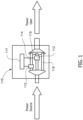
- FIG. 1 illustrates a block diagram of an exemplary utility meter 110 including an exemplary sensor device 112.
- utility meter 110 includes sensor device 112, a conductor 114, and a meter control board 117 coupled to sensor device 112.
- Conductor 114 may include a bus bar, multi-strand wire, single-strand wire, cable, or other suitable conductor to transmit electricity from a power source to a power user.
- the power source may include, without limitation, an electrical grid and/or a power generator system, such as a gas turbine engine, a hydroelectric turbine, a wind turbine, a solar panel, and/or another suitable generation and/or transmission system.
- the power source may also include a smart-grid in communication with meter control board 117.
- a user may include, without limitation, a residential user, a commercial user and/or any other user of electricity at any level.
- Sensor device 112 is coupled to conductor 114 to sense current flowing through conductor 114.
- Sensor device 112 provides a signal representative of sensed current to meter control board 117. Based on the signal received from sensor device 112, meter control board 117 determines an amount of electricity transmitted through conductor 114 from the power source to the user over time.
- sensor device 112 is highly accurate to ensure the user is charged substantially only for electricity received, rather than being charged for substantially all the electricity transmitted to the user by the operator of the power source.
- utility meter 110 further includes conductors 115 and 116 and another sensor device 112 coupled to conductor 115.
- conductors 115 and 116 may be used in other utility meter embodiments.
- sensor device 112 is not limited to only being used within utility meter 110, but may be utilized in virtually any application to sense current through a conductor, such as power generation applications, utility applications, automotive applications, appliance applications, telecommunication applications, etc.
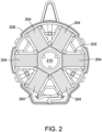
- FIG. 2 illustrates a partially disassembled view of exemplary sensor device 112.
- sensor device 112 includes a substrate 202, a coil 204 including a plurality of turns wound about substrate 202, and a dielectric material 208.
- Coil 204 includes an aperture 210 defined therein, which is structured (e.g., by size, orientation, and/or shape, etc.) to receive conductor 114 therein.
- Dielectric material 208 is positioned adjacent to coil 204 and at least partially within aperture 210. More specifically, in this embodiment, dielectric material 208 is positioned at least partially between coil 204 and conductor 114, when conductor 114 is positioned through aperture 210.
- Dielectric material 208 may include one or more dielectric materials having a variety of characteristics configured in a variety of ways. Dielectric material 208 has at least one thickness, and may have various thicknesses. In the exemplary embodiment, dielectric material 208 positioned adjacent to coil 204 and at least partially within aperture 210 has a thickness of about 3.0 millimeters. Also, in the same embodiment, dielectric material 208 positioned adjacent to coil 204 but opposite aperture 210 has a thickness of about 1.2 millimeters. It should be appreciated that dielectric material 208 may have any thickness or thicknesses, that enables sensor device 112 to function as described herein.
- thickness of dielectric material 208 is selected, at least partially based on the dielectric constant of dielectric material 208, the proximity of coil 204 to one or more conductors 114, 115 and 116 (shown in FIG. 1 ), and/or space available in an intended environment for installation of the sensor device, etc.
- the thickness of dielectric material 208 may range from about 1.0 millimeter to about 3.0 centimeters, or greater in still other embodiments.
- dielectric material 208 may be fabricated from one or more of several types of material, such as, without limitation, plastic materials, thermoplastic materials, thermoset materials, ceramic materials, metallic materials, wood materials, clay materials, organic materials, any mixture thereof, and/or other materials suitable to perform as described herein.
- dielectric material 208 includes a PBT thermoplastics material commercially available from a Valox ® family of materials.
- dielectric material 208 includes one or more of, without limitation, Kapton ® tape, a polyvinylidene fluoride (PVDF) material, a room temperature vulcanized silicone (RTV) polymer, a PBT thermoplastics material commercially available from a Valox ® family of materials (e.g., Valox ® 365 or Valox ® V9561), a polyethylene terephthalate (PET) thermoplastic material from the Rynite ® family of materials, a PPS thermoplastic material commercially available from the Ryton ® family of materials, a PPS thermoplastic material commercially available from the Primef ® family of materials, a nylon thermoplastic material commercially available from the Zytel ® , Stanyl ® , or RTP ® families of materials, a LCP thermoplastic material (e.g., Sumitomo ® E5008L or E4008L materials), etc.
- PVDF polyvinylidene fluoride
- RTV room temperature vulcanized silicone
- dielectric material 208 may be selected based on dielectric constant, suitability for one or more manufacturing techniques, dimensional stability, cost, moldability, workability, rigidity, and/or other characteristic of the material(s). In at least one example, dielectric material 208 is selected at least partially based on the variability of its dielectric constant over temperature.
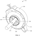
- FIG. 3 is a perspective view of sensor device 112 (shown as assembled) with conductor 114 extending through aperture 210.
- sensor device 112 senses current flow through conductor 114. Specifically, when current flows through conductor 114, a current is induced in coil 204 (shown in FIG. 2 ). The amount of current induced in coil 204 is representative of the amount of current flowing through conductor 114.
- coil 204 is spaced a distance from conductor 114. Accordingly, capacitance exists between coil 204 and conductor 114. The capacitance may affect the accuracy of sensor device 112 at different operating voltages.
- dielectric material 208 is positioned within at least a portion of an air-gap 306 defined between coil 204 and conductor 114.
- the reduction in capacitance enables sensor device 112 to sense current flowing through conductor 114 with improved accuracy, as compared to known Rogowski coils or other air-gap coils. More specifically, by reducing capacitance coupling between coil 204 and conductor 114, the sensitivity to operating voltage is reduced. As a result, consistent current sensing is provided at different operating voltages across a range of different currents, including high and low currents. Accordingly, when sensor device 112 is included in utility meter 110 (shown in FIG. 1 ), one or more processes necessary for calibrating known sensor devices may be omitted. Specifically, in the exemplary embodiment, the consistency of sensor device 112 to accurately detect current across different operating voltages may permit meter control board 117 (shown in FTG.
- sensor device 112 includes a housing 312.
- Housing 312 may be formed from a variety of materials and/or through a variety of fabrication processes.
- housing 312 includes substantially only dielectric material 208, such that dielectric material 208 is positioned about coil 204, opposite aperture 210 (as shown in FIG. 2 ).
- sensor device 112 when used within utility meter 110 having three-phase conductors 114, 115, and 116 (shown in FIG. 1 ), sensor device 112 may be positioned about conductor 114 and proximate to at least one other conductor 115 (as shown in Fig. 1 ), and potentially proximate to conductor 116.
- dielectric material 208 is positioned between coil 204 and adjacent conductor 115.
- housing 312 may include one or more materials in addition to dielectric material 208, such as non-dielectric materials or dielectric materials that have different characteristics.
- housing 312 includes dielectric material 208 and an additive material, which is provided to support dielectric material 208 in one or more locations relative to coil 204 to enable it to perform as described herein.
- the additive material may include plastic materials, thermoplastic materials, thermoset materials, ceramic materials, metallic materials, wood materials, clay materials, organic materials, any mixture thereof, and/or other suitable materials.
- the additive material may be selected based on manufacturing techniques, dimensional stability, cost, moldability, workability, rigidity, and/or other characteristics of the material, etc.
- dielectric material 208 when dielectric material 208 is a higher cost material (as compared to the additive material); the inclusion of an additive material may reduce the overall cost of sensor device 112. Further, one or more additive materials may be used to perform one or more additional functions, such as supporting dielectric material 208, protecting and/or insulating coil 204, etc. As should be apparent, the additive material may be used as part of housing 312 in various embodiments. In the exemplary embodiment, however, an additive material is omitted, as housing 312 substantially only includes dielectric material 208.
- Housing 312 may be fabricated from the dielectric material, formed integrally from dielectric material 208 and at least one additive material, or assembled from separate dielectric material(s) 208 and additive material(s). Housing 312 and/or dielectric material 208 may be fabricated using one or more injection molding processes and/or other suitable fabrication processes. In the exemplary embodiment, housing 312 is constructed via a single injection molding process, in which dielectric material 208 is injected into a mold structured to form housing 312.
- housing 312 may be constructed from a multi-stage injection molding process.
- a multi-stage process an additive material is molded into a specific shape through an initial molding process. Subsequently, the molded additive material is positioned within a mold, and dielectric material 208 is injected into the mold. Dielectric material 208 flows into voids defined between the mold and/or the additive material, to form housing 312 from dielectric material 208 and additive material.
- a multi-stage molding process may permit a relatively high-cost dielectric material to be specifically positioned relative to coils 204 such that desired performance as described herein is achieved, while still permitting other portions of housing 312 to be constructed from one or more relatively low cost materials.
- housing 312 may be constructed by other fabrication techniques to provide dielectric material 208 throughout or at desired positions relative to coil 204 and/or conductor 114.
- dielectric material 208 is constructed separately from an additive material, and subsequently transformed and/or constructed with the additive material to form housing 312.
- a tubular dielectric material may be inserted into an aperture formed by an additive material to form housing 312.
- housing 312 includes one or more spacers 316 that surround the aperture 210.
- spacers 316 When conductor 114 is received in aperture 210 (as shown in Fig. 3 ), an air-gap 306 is formed between housing 312 and conductor 114. Simultaneously, a friction fit is created between spacers 316 and conductor 114.
- Spacers 316 are offset from aperture 210 by an offset ring 308. Spacers 316 and offset ring 308 may include dielectric material 208 and/or another material. It should be appreciated that spacers 316 may be formed in a variety of different shapes that are designed to receive and/or couple to various types, shapes, and/or orientations of conductors.
- spacers 316 are shaped as crush ribs with curved points.
- the crushed ribs maintain a pressure on conductor 114 to prevent housing 312 from moving in relation to conductor 114.
- offset ring 308 provides reinforcement to spacers 316 and is formed of a rigid material as described above. Offset ring 308 also ensures that sensor device is spaced a distance away from any other object in meter 110 that may be touching conductor 114.
- the electromagnetic field of conductor 114 changes when conductor is being touched by another object, especially one that conducts electricity, such as a clip. By offsetting sensor device 112 from other objects touching conductor 114, sensor device 112 can provide more accurate readings.
- Housing 312 also includes at least one rotational positioner 320.
- Rotational positioner 320 prevents coil 204 from rotating around conductor 114.
- the position of coil 204 in relation to conductor 114 and to conductors 115 and 116 affects the accuracy of sensor device 112, when sensor device 112 is surrounding conductor 114.
- Rotating coil 204 in the electromagnetic fields generated by those conductors can affect the calibration of sensor device 112 and thus the accuracy.
- housing 312 includes rotational positioner 320.
- Rotational positioner 320 prevents rotary movement when placed against a corner or rib in meter 110.
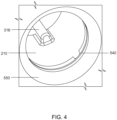
- FIG. 4 illustrates a close-up view of aperture 210 defined by sensor device 112, in accordance with one embodiment of the disclosure.
- Offset ring 308 offsets spacers 316 from aperture 210. Offset ring 308 allows spacers 316 to maintain sensor device's 112 position relative to conductor 114, while not interfering between conductor 114 and coil 204. In the exemplary embodiment, spacers 316 do not radially extend into aperture 210 more than one third of the thickness of aperture 210. This is to prevent the material comprising spacers 316 from interfering with the amount of material between coil 204 and conductor 114.
- offset ring 308 and spacers 316 are structured to form a friction fit with a rectangular-shaped bus bar conductor.
- FIG. 5 illustrates the assembly of housing 312 of sensor device 112, in accordance with one embodiment of the disclosure.
- Housing 312 includes a first portion 505 and a second portion 510.
- First portion 505 is releasably coupled to second portion 510 such that substrate 202 and coil 204 are substantially enclosed therein.
- first portion 505 is coupled to second portion 510 with a major ship-lap joint 540 and a minor ship-lap joint 545 to form housing 312.
- first portion 505 and second portion 510 may be coupled together through a variety of different methods, including, without limitation, one or more butt joints, screw joints, hinge joints, tab-slot arrangements, tongue-and-groove arrangements, fasteners, etc.
- housing 312 has generally toroidal shape, it should be appreciated that other enclosure embodiments may define any shape and/or size, that is sized and/or operates to at least partially enclose substrate 202 and coil 204, and that enables dielectric material 208 to perform as described herein.
- the thickness of dielectric material 208 varies throughout housing 312.
- Each ship-lap joint 540 and 545 between first portion 505 and second portion 510 provides an overlap of first portion 505 and second portion 510.
- first portion 505 and second portion 510 each have a thickness of about 1.2 millimeters at aperture 210.
- first portion 505 and second portion 510 at least partially overlap at the major ship-lap joint 540 (along aperture 210) to create a total thickness of about 2.4 millimeters.
- first portion 505 and second portion 510 are structured such that the total thickness about the outside of housing 312 at a minor ship-lap joint 545 (opposite aperture 210) is less than about 1.2 millimeters. It should be appreciated that various methods of forming housing 312 may be used to provide one or more different thicknesses of housing 312 and/or dielectric material 208.
- the major ship-lap joint 540 runs along a substantial portion of aperture 210. This is to provide a longer path for potential arcs between coil 204 and conductor 114.
- the thickness of housing 312 and/or dielectric material 208 may be between about 0.5 millimeters and about 3.0 centimeters. In some embodiments, one or more thicknesses of housing 312 and/or dielectric material 208 are between about 1.0 millimeters and 6.0 millimeters. Further, in various embodiments, one or more thicknesses of housing 312 and/or dielectric material 208 are between about 1.0 millimeters and 4.0 millimeters. It should be appreciated that housing 312 and/or dielectric material 208 may have different thickness in other embodiments, potentially based on a method of assembly/fabrication, the characteristic(s) of a selected dielectric material, and/or desired performance characteristic(s). Further, other shapes, sizes, and/or joints for housing 312 may be used to at least partially enclosure coil 204, while positioning dielectric material 208 relative to coil 204 to perform consistent with one or more aspects of the present disclosure.
- First portion 505 and second portion 510 also include a connection ring 525, an edge bevel 550, a side wall 530, and an outer wall 535.
- the thickness of side wall 530 is less than that of combined thicknesses of first portion 505 and second portion 510 along aperture 210.
- Connection ring 525, on both first portion 505 and second portion 510 is where major ship-lap joint 540 of first portion 505 and second portion 510 connect.
- Connection ring 525 has the same thickness as the combined thicknesses of first portion 505 and second portion 510 at major ship-lap joint 540.
- Edge bevel 550 connects connection ring 525 to side wall 530.
- edge bevel 550 As edge bevel 550 goes from connection ring 525 to side wall 530, the thickness of edge bevel 550 slowly reduces. Where the thickness of edge bevel 550 starts at the thickness of connection ring 525 and slowly and consistently reduces to the thickness of side wall 530. Edge bevel's 550 consistent changes in thickness, prevents interruption in the electromagnetic field that may occur from abrupt changes in the amount of dielectric material 208 in the electromagnetic field.
- minor ship-lap joint 545 When first portion 505 and second portion 510 are coupled, minor ship-lap joint 545 is formed along outer wall 535. Minor slip-lap joint 545 runs around the circumference of outer wall 535 when first portion 505 and second portions 510 are coupled. Both major ship-lap joint 540 and minor slip-lap joint 545 retain a clearance between first portion 505 and second portion 510. In the exemplary embodiment, this clearance is between 0.076 mm and 0.127 mm (0.003 inches and 0.005 inches). The clearance is created when coil 204 is sandwiched between first portion 505 and second portion 510.
- Coil 204 and substrate 202 are sized so that when first portion 505 and second portion 510 are coupled around coil 204 and substrate 202, the fit creates the aforementioned clearance while housing 312 maintains a constant pressure on coil 204 and further prevents coil 204 from moving in relation to first portion 505.
- coil 204 includes an exemplary Rogowski coil. It should be appreciated; however, that sensor device 112 may include a coil other than a Rogowski coil. Further, aspects of the present disclosure are not limited to only being used with a Rogowski coil as described and illustrated herein.
- First portion 505 includes retaining portions 515 and second portion 510 includes U-clips 520.
- U-clips 520 and retaining portions 515 attach first portion 505 to second portion 510.
- FIG. 6 illustrates a close-up of the first portion 505 of housing 312 and one of the retaining portions 515.
- FIG. 7 illustrates a close-up of assembled sensor device 112 showing U-clip 520 attached to retaining portion 515.
- outer wall 535 includes a recessed area for receiving U-clip 520. As shown in FIG 7 , when U-clip 520 is coupled to retaining portion 515, U-clip 520 and retaining portion 515 don't extend past outer wall 535.
- U-Clip 520 and retaining portion 515 flush with outer wall 535 prevents U-clip 520 from catching on external items or snapping off.
- FIG. 8 displays first portion 505 of housing 312 with a layer of epoxy 810 for coupling coil 204 (shown in FIG. 2 ) to first portion 505.
- epoxy 810 is a high temperature epoxy, such as Epoxy Resin 6060RP-6 manufactured by Plenox-Wells Electronic Material Co., Ltd. A high temperature epoxy is used to resist the decay of epoxy 810 at high temperatures over time.
- epoxy 810 is placed in first portion 505.
- Coil 204 is placed into first portion 505 into epoxy 810.
- second portion 510 (shown in FIG. 5 ) is coupled to first portion 505 so that coil 204 is firmly pressed into epoxy 810.
- Epoxy 810 spreads out to fill empty spaces between first portion 505 and coil 204.
- the first portion 505 and second portion 510 serve as a holding force while epoxy 810 sets-up/cures to solid, without requiring heating or special treatment of epoxy 810.
- FIG. 9 is a perspective view of substrate 202 and coil 204 separated from housing 312, shown in FIG. 3 .
- substrate 202 includes six bobbins 902, 904, 906, 908, 910, and 912 (collectively referred to as bobbins 902-912).
- Each bobbin 902-912 has a substantially circular cross-section, and more particular, is a right cylinder that includes flanges 914 at opposite ends that retain coil 204.
- substrate 202 may have a different number, shape, and/or size of bobbins.
- substrate 202 may include five bobbins, eight bobbins, ten bobbins, thirty bobbins, or another even or odd number of bobbins.
- substrate 202 may include bobbins having a different shape, and/or an ovular cross-section, an elliptical cross-section, or rectangular cross-section, etc.
- substrate 202 may include a different structure for supporting coil 204, in addition to or other than flanges 914.
- coil 204 is sufficient rigid to omit substrate 202.
- bobbins 902-912 are coupled together via hinged joints 916. More specifically, bobbins 902 and 904 are hingedly coupled to permit pivotal movement there between. In various embodiments, bobbins 902-912 may be linearly aligned to enable efficient winding of coil 204 and/or pivoted relative to one another to form a substantially circular shape, as illustrated in Fig. 9 .
- Each of bobbins 902-912 of substrate 202 is a non-magnetic structure, such that bobbins 902-912 are constructed from one or more non-magnetic materials, including, for example, thermoplastic material, ceramic material, wood, material, or other kinds of suitable material(s).
- each of bobbins 902-912 is fabricated from a dielectric material, potentially consistent with dielectric material 208.
- substrate 202 is shaped and/or sized to provide improved mounting within utility meter 110 and/or to a meter control board 117 (both shown in FIG.
- bobbins 902-912 are formed separate from housing 312. It should be appreciated, however, that bobbins 902-912 may be formed integrally with and/or form one or more portions of housing 312 in other sensor device embodiments.
- coil 204 is wound multiple turns on each bobbin 902-912. More specifically, in the exemplary embodiment, coil 204 includes a single magnet wire that enables coil 204 to be wound from bobbin 902 to bobbin 912 with several turns on each bobbin 902-912, and then wound back to bobbin 902 with additional turns on each bobbin 902-912. It should be appreciated that, in other embodiments, other different winding patterns on bobbins 902-912 may be used. Consistent with the above winding pattern across bobbins 902-912, a first end and a second end of coil 204 terminates at bobbin 902.
- FIG. 10 illustrates a partial cross-sectional view of sensor device 112 at bobbin 902.
- bobbin 902 includes a first shield 1005 and a second shield 1010.
- First shield 1005 is positioned between bobbin 902 and coil 204.
- Second shield 1010 is positioned adjacent to coil 204 and opposite from first shield 1005, such that coil 204 is positioned between first shield 1005 and second shield 1010.
- Each bobbin 902-912 includes substantially the same shield-coil-shield pattern as shown in Fig. 10 .
- bobbins 902-912 may include other winding patterns, including winding patterns, in which the winding pattern varies from one bobbin to another bobbin.
- each shield 1005 and 1010 provides a Faraday shield. More specifically, in this exemplary embodiment, first and second shields 1005 and 1010 behave substantially consistent with a Faraday cage, in order to facilitate reducing common mode noise on the sensor device 112 and/or to provide a low-pass filter for high frequency noise filtering. As a result, first and second shield 1005 and 1010 facilitate improved performance in the context of one or more industry standards for electromagnetic interface (EMI) and/or electromagnetic compatibility (EMC).
- EMI electromagnetic interface
- EMC electromagnetic compatibility
- first shield 1005 and second shield 1010 are formed from a single magnet wire.
- first shield 1005 and second shield 1010 may include any suitable materials, such as, without limitation, copper, aluminum or other nonferrous conducting material.
- the shielding material may be formed as a sheet, a tape, a wire, a spray and/or any other form that enables bobbins 902-912 to include shields 1005 and 1010.
- application of shields 1005 and/or 1010 may be formed, without limitation, via winding, wrapping, and/or spraying, for example.
- first and second shield 1005 and 1010 may be formed separately from coil 204 and subsequently applied to coil 204.
- FIG. 11 is a cut-away view of a utility meter 110 with two sensor devices 112 measuring two conductors 114 and 115.
- a meter housing 1105 encloses sensor devices 112 and conductors 114 and 115.
- Each rotational positioner 320 of each sensor device 112 is positioned in the corner of meter housing 1105 to prevent rotational movement of the corresponding sensor device 112.
- FIG. 12 is a cut-away view of a utility meter 110 with three sensor devices measuring three conductors 114, 115, and 116.
- Meter housing 1105 includes three ribs 1202, 1204, and 1206. Ribs 1202, 1204, and 1206 couple to rotational positioners 320, thereby preventing rotational movement of sensor devices. It should be appreciated, however, that rotational positioners 320 may be positioned or used in other manners to prevent rotational movement in other sensor device embodiments.
- the sensor devices, utility meters, and methods described herein may provide a highly-accurate sensor device that provides an expanded operating range with reduced calibration requirements over known coil sensors.
- the disclosed dielectric material may provide reduced capacitance between a coil and one or more conductors, thereby providing improved accuracy across a range of currents and/or voltages. The improved accuracy may be realized with fewer calibration processes during manufacturing, resulting in reduced manufacturing cost and/or time.
- the disclosed shielding techniques provide improved rejection of EMI, originating from other electronics and/or tampering devices.
- the above described embodiments provide systems and methods for preventing the coil of a sensor device from moving in relation to the conductor that the sensor device is measuring. More specifically, the sensor devices when used in utility meters will provide high accuracy measurement of current through conductors over a period of many years. By preventing the coil from moving, the calibration of the sensor devices will stay the same and ensure accurate measurements for many years.
Landscapes
- Physics & Mathematics (AREA)
- General Physics & Mathematics (AREA)
- Engineering & Computer Science (AREA)
- Power Engineering (AREA)
- Measuring Instrument Details And Bridges, And Automatic Balancing Devices (AREA)
- Transformers For Measuring Instruments (AREA)
Applications Claiming Priority (1)
| Application Number | Priority Date | Filing Date | Title |
|---|---|---|---|
| US14/454,861 US9671434B2 (en) | 2014-08-08 | 2014-08-08 | Sensor devices and methods for use in sensing current through a conductor |
Publications (2)
| Publication Number | Publication Date |
|---|---|
| EP2982993A1 EP2982993A1 (en) | 2016-02-10 |
| EP2982993B1 true EP2982993B1 (en) | 2023-05-03 |
Family
ID=53724075
Family Applications (1)
| Application Number | Title | Priority Date | Filing Date |
|---|---|---|---|
| EP15178311.5A Active EP2982993B1 (en) | 2014-08-08 | 2015-07-24 | Sensor device for use in sensing current through a conductor and utility meter manufacturing method |
Country Status (7)
| Country | Link |
|---|---|
| US (1) | US9671434B2 (enExample) |
| EP (1) | EP2982993B1 (enExample) |
| JP (1) | JP6674206B2 (enExample) |
| CN (1) | CN105372473B (enExample) |
| BR (1) | BR102015018819B1 (enExample) |
| CA (1) | CA2898935C (enExample) |
| MX (1) | MX349278B (enExample) |
Families Citing this family (13)
| Publication number | Priority date | Publication date | Assignee | Title |
|---|---|---|---|---|
| CN105723228A (zh) * | 2013-09-10 | 2016-06-29 | 莫列斯有限公司 | 具有传感器的连接器 |
| US9671434B2 (en) | 2014-08-08 | 2017-06-06 | Aclara Meters Llc | Sensor devices and methods for use in sensing current through a conductor |
| KR101966749B1 (ko) * | 2015-12-11 | 2019-04-08 | 주식회사 아모그린텍 | 자기차폐형 변류기 |
| EP3379269B1 (fr) * | 2017-03-24 | 2022-11-16 | TE Connectivity Solutions GmbH | Accessoire de contrôle pour un appareil électrique pourvu d'une borne de raccordement |
| BE1026245B1 (de) * | 2018-05-04 | 2019-12-02 | Phoenix Contact Gmbh & Co | Stromsensor |
| WO2020011732A1 (en) * | 2018-07-11 | 2020-01-16 | Lem International Sa | Current transducer with integrated primary conductor |
| US11315725B2 (en) * | 2018-11-02 | 2022-04-26 | Analog Devices International Unlimited Company | Current sensing coil electrostatic shielding |
| USD895550S1 (en) * | 2019-03-18 | 2020-09-08 | Yokogawa Electric Corporation | Sensor device |
| USD892739S1 (en) * | 2019-03-18 | 2020-08-11 | Yokogawa Electric Corporation | Sensor device |
| US11137419B2 (en) * | 2019-12-17 | 2021-10-05 | Analog Devices International Unlimited Company | Mutiple range current sensor techniques |
| FI20205764A1 (en) * | 2020-07-21 | 2022-01-22 | Safegrid Oy | APPARATUS AND TOOL FOR MEASURING COIL |
| AT525335B1 (de) * | 2021-07-21 | 2024-09-15 | Egston System Electronics Eggenburg Gmbh | Stromsensorspulenanordnung |
| EP4439082A1 (en) * | 2023-03-30 | 2024-10-02 | Abb Schweiz Ag | Current sensing device |
Citations (3)
| Publication number | Priority date | Publication date | Assignee | Title |
|---|---|---|---|---|
| US4408175A (en) * | 1982-01-18 | 1983-10-04 | Honeywell Inc. | Self centering current responsive pickup means |
| US20060006976A1 (en) * | 2004-07-07 | 2006-01-12 | Veris Industries, Llc | Split core sensing transformer |
| US20130320961A1 (en) * | 2012-05-31 | 2013-12-05 | Pulse Electronics, Inc. | Current sensing devices and methods |
Family Cites Families (63)
| Publication number | Priority date | Publication date | Assignee | Title |
|---|---|---|---|---|
| US3340353A (en) | 1966-01-28 | 1967-09-05 | Dow Chemical Co | Double-shielded electric cable |
| CA1182537A (fr) | 1983-02-08 | 1985-02-12 | Hubert P. Mercure | Capteur dynamique de courant |
| FR2564594B1 (fr) | 1984-05-21 | 1986-09-12 | Merlin Gerin | Capteur de courant a noyau amagnetique |
| US4795973A (en) * | 1984-11-08 | 1989-01-03 | Niagara Mohawk Power Corporation | Line mounted apparatus for measuring line potential |
| US4700131A (en) | 1986-04-07 | 1987-10-13 | Westinghouse Electric Corp. | Mutual inductor current sensor |
| JPH0543510Y2 (enExample) * | 1988-09-29 | 1993-11-02 | ||
| DE9005965U1 (de) * | 1989-05-29 | 1990-08-02 | Kitagawa Industries Co., Ltd., Nagoya, Aichi | Elektrischer Rauschabsorber |
| FR2692074B1 (fr) | 1992-06-05 | 1994-07-22 | Alsthom Gec | Bobine de rogowski. |
| FR2695482B1 (fr) | 1992-09-10 | 1994-10-21 | Alsthom Gec | Dispositif de mesure utilisant une bobine des Rogowski. |
| US5502374A (en) * | 1994-09-02 | 1996-03-26 | Veris Industries, Inc. | Current sensors |
| DE19505812C2 (de) | 1995-02-09 | 1997-02-06 | Siemens Ag | Stromerfassungsspule für einen Stromwandler |
| ES2183927T3 (es) | 1996-06-21 | 2003-04-01 | Pirelli Cavi E Sistemi Spa | Composicion aislante resistente a un arbol de agua. |
| ES2260847T3 (es) | 1997-08-28 | 2006-11-01 | General Electric Company | Detector de corriente autoalimentado. |
| AU3617899A (en) | 1998-04-22 | 1999-11-08 | Power Electronic Measurements Limited | A current measuring device |
| AU4183399A (en) | 1998-05-07 | 1999-11-23 | Airpax Corporation, L.L.C. | Ac current sensor having high accuracy and large bandwidth |
| WO2000043795A1 (en) * | 1999-01-21 | 2000-07-27 | Tdk Corporation | Current sensor |
| JP3437805B2 (ja) * | 1999-10-07 | 2003-08-18 | 大崎電気工業株式会社 | 電子式電力量計 |
| US6313623B1 (en) | 2000-02-03 | 2001-11-06 | Mcgraw-Edison Company | High precision rogowski coil |
| US6717397B2 (en) | 2000-04-17 | 2004-04-06 | Suparules Limited | Current measurement device |
| DE20101454U1 (de) | 2001-01-27 | 2001-05-23 | Phoenix Contact Gmbh & Co., 32825 Blomberg | Stromsensor auf Leiterplattenbasis |
| JP2003075474A (ja) * | 2001-09-03 | 2003-03-12 | Sumitomo Electric Ind Ltd | 架空地線の電流検出装置 |
| JP2003130894A (ja) | 2001-10-29 | 2003-05-08 | Toshiba Corp | 変流器 |
| JP2004119926A (ja) | 2002-09-30 | 2004-04-15 | Toshiba Corp | 変流器及び変流器システム |
| CA2432671C (en) | 2003-06-17 | 2008-11-04 | Kinectrics Inc. | Coreless current sensor |
| FR2870040B1 (fr) | 2004-05-10 | 2006-06-09 | Areva T & D Sa | Transformateur de courant a bobinages de type rogowski comportant des circuits partiels associes pour former un circuit complet |
| FR2870350B1 (fr) | 2004-05-13 | 2006-07-14 | Schneider Electric Ind Sas | Dispositif de mesure d'un courant electrique, capteur de courant, declencheur electrique et dispositif de coupure comportant un tel dispositif de mesure |
| GB0412129D0 (en) | 2004-05-29 | 2004-06-30 | Lem Heme Ltd | Improvements in and relating to current measuring apparatus |
| JP4418332B2 (ja) * | 2004-09-09 | 2010-02-17 | 矢崎総業株式会社 | 電流センサ |
| US7253603B2 (en) | 2005-01-06 | 2007-08-07 | S & C Electric Co. | Current sensor arrangement |
| US7227441B2 (en) | 2005-02-04 | 2007-06-05 | Schweitzer Engineering Laboratories, Inc. | Precision Rogowski coil and method for manufacturing same |
| US7227442B2 (en) | 2005-04-01 | 2007-06-05 | Schweitzer Engineering Laboratories, Inc. | Precision printed circuit board based rogowski coil and method for manufacturing same |
| EP1960796B1 (en) | 2005-11-28 | 2014-05-07 | Ladislav Grno | Precision flexible current sensor |
| JP4674533B2 (ja) | 2005-12-02 | 2011-04-20 | パナソニック電工株式会社 | 交流電流検出用コイル |
| JP4916821B2 (ja) | 2006-03-31 | 2012-04-18 | 株式会社ダイヘン | 電圧検出用プリント基板及びそれを用いた電圧検出器 |
| US7545138B2 (en) | 2006-07-06 | 2009-06-09 | Schweitzer Engineering Laboratories, Inc. | Precision, temperature-compensated, shielded current measurement device |
| US7532000B2 (en) | 2006-08-03 | 2009-05-12 | The Boeing Company | Method and system for measurement of current flows in fastener arrays |
| US7579824B2 (en) | 2006-09-29 | 2009-08-25 | Gm Global Technology Operations, Inc. | High-precision Rogowski current transformer |
| US7538541B2 (en) | 2006-11-06 | 2009-05-26 | Cooper Technologies Company | Split Rogowski coil current measuring device and methods |
| US7564233B2 (en) | 2006-11-06 | 2009-07-21 | Cooper Technologies Company | Shielded Rogowski coil assembly and methods |
| DE102006061923A1 (de) | 2006-12-21 | 2008-07-03 | Siemens Ag | Rogowski-Sensor und Verfahren zum Messen eines Stromes |
| US7598724B2 (en) | 2007-01-19 | 2009-10-06 | Admmicro Properties, Llc | Flexible current transformer assembly |
| CA2609611A1 (en) * | 2007-09-10 | 2009-03-10 | Veris Industries, Llc | Split core status indicator |
| KR100965818B1 (ko) | 2008-05-13 | 2010-06-24 | 태화트랜스 주식회사 | 로고스키코일을 구비하는 분할클램프식 전류센서 |
| ITBO20080084U1 (it) | 2008-11-18 | 2010-05-19 | Lorenzo Peretto | Sistema costruttivo per sensore di corrente e/o di tensione elettrica |
| US7986202B2 (en) * | 2008-12-18 | 2011-07-26 | Woodson Cameron L | Circuit breaker current transformer conductor location device for improved sensing accuracy and assembly |
| US9151782B2 (en) * | 2009-07-31 | 2015-10-06 | Pulse Electronics, Inc. | Current sensing devices and methods |
| US9823274B2 (en) | 2009-07-31 | 2017-11-21 | Pulse Electronics, Inc. | Current sensing inductive devices |
| US9664711B2 (en) | 2009-07-31 | 2017-05-30 | Pulse Electronics, Inc. | Current sensing devices and methods |
| CN201465698U (zh) | 2009-08-14 | 2010-05-12 | 河南电力试验研究院 | 一种高精度开口式罗氏线圈 |
| US20110043190A1 (en) | 2009-08-20 | 2011-02-24 | Farr Lawrence B | Rogowski coil, medium voltage electrical apparatus including the same, and method of providing electrostatic shielding for a rogowski coil |
| US8487606B2 (en) | 2010-10-26 | 2013-07-16 | Eaton Corporation | Sensor assembly, trip unit including the same, and method of manufacturing a sensor assembly |
| US8872611B2 (en) | 2011-08-18 | 2014-10-28 | General Electric Company | Rogowski coil assemblies and methods for providing the same |
| US9081040B2 (en) * | 2011-09-09 | 2015-07-14 | General Electric Company | Sensor devices and methods for use in sensing current through a conductor |
| US9075091B2 (en) | 2011-09-09 | 2015-07-07 | General Electric Company | Sensor devices and methods for use in sensing current through a conductor |
| US8829888B2 (en) | 2011-09-09 | 2014-09-09 | General Electric Company | Sensor devices and methods for use in sensing current through a conductor |
| US9429595B2 (en) * | 2011-09-09 | 2016-08-30 | Aclara Meters Llc | Sensor devices and methods for use in sensing current through a conductor |
| US8912807B2 (en) | 2011-09-09 | 2014-12-16 | General Electric Company | Sensor devices and methods for use in sensing current through a conductor |
| CN202351323U (zh) | 2011-11-22 | 2012-07-25 | 李云宏 | 采用罗氏线圈电流互感器的电力数字仪表 |
| DE102012201992A1 (de) | 2012-02-10 | 2013-08-14 | Siemens Aktiengesellschaft | Kombinationswandleranordnung und Schaltgerät |
| EP2722679A1 (en) | 2012-10-18 | 2014-04-23 | ABB Technology AG | Fastening means for current and/or voltage sensor |
| CN103630723A (zh) | 2013-11-25 | 2014-03-12 | 北京航空航天大学 | 一种适用于罗氏线圈电流传感器的罗氏线圈传感头 |
| EP2980592A1 (en) * | 2014-07-30 | 2016-02-03 | General Electric Company | Sensor devices and methods for use in sensing current through a conductor |
| US9671434B2 (en) | 2014-08-08 | 2017-06-06 | Aclara Meters Llc | Sensor devices and methods for use in sensing current through a conductor |
-
2014
- 2014-08-08 US US14/454,861 patent/US9671434B2/en active Active
-
2015
- 2015-07-24 EP EP15178311.5A patent/EP2982993B1/en active Active
- 2015-07-30 CA CA2898935A patent/CA2898935C/en active Active
- 2015-08-05 JP JP2015154666A patent/JP6674206B2/ja active Active
- 2015-08-05 BR BR102015018819-6A patent/BR102015018819B1/pt active IP Right Grant
- 2015-08-07 MX MX2015010282A patent/MX349278B/es active IP Right Grant
- 2015-08-07 CN CN201510588888.XA patent/CN105372473B/zh active Active
Patent Citations (3)
| Publication number | Priority date | Publication date | Assignee | Title |
|---|---|---|---|---|
| US4408175A (en) * | 1982-01-18 | 1983-10-04 | Honeywell Inc. | Self centering current responsive pickup means |
| US20060006976A1 (en) * | 2004-07-07 | 2006-01-12 | Veris Industries, Llc | Split core sensing transformer |
| US20130320961A1 (en) * | 2012-05-31 | 2013-12-05 | Pulse Electronics, Inc. | Current sensing devices and methods |
Also Published As
| Publication number | Publication date |
|---|---|
| CA2898935A1 (en) | 2016-02-08 |
| CN105372473A (zh) | 2016-03-02 |
| EP2982993A1 (en) | 2016-02-10 |
| BR102015018819B1 (pt) | 2022-03-29 |
| US20160041204A1 (en) | 2016-02-11 |
| MX2015010282A (es) | 2016-04-04 |
| CN105372473B (zh) | 2019-02-05 |
| CA2898935C (en) | 2022-11-15 |
| MX349278B (es) | 2017-07-20 |
| BR102015018819A2 (pt) | 2016-02-10 |
| US9671434B2 (en) | 2017-06-06 |
| JP2016038383A (ja) | 2016-03-22 |
| HK1221773A1 (zh) | 2017-06-09 |
| JP6674206B2 (ja) | 2020-04-01 |
Similar Documents
| Publication | Publication Date | Title |
|---|---|---|
| EP2982993B1 (en) | Sensor device for use in sensing current through a conductor and utility meter manufacturing method | |
| EP2568298B1 (en) | Current sensor and method of manufacturing thereof | |
| EP2568299B1 (en) | Sensor devices and methods for use in sensing current through a conductor | |
| EP2568300B1 (en) | Sensor devices and methods for use in sensing current through a conductor | |
| US8829888B2 (en) | Sensor devices and methods for use in sensing current through a conductor | |
| US9081040B2 (en) | Sensor devices and methods for use in sensing current through a conductor | |
| CA2897856C (en) | Sensor devices and methods for use in sensing current through a conductor | |
| EP2625699B1 (en) | Multifunctional measuring device | |
| HK1221773B (zh) | 用於感测穿过导体的电流的传感器装置和方法 |
Legal Events
| Date | Code | Title | Description |
|---|---|---|---|
| PUAI | Public reference made under article 153(3) epc to a published international application that has entered the european phase |
Free format text: ORIGINAL CODE: 0009012 |
|
| AK | Designated contracting states |
Kind code of ref document: A1 Designated state(s): AL AT BE BG CH CY CZ DE DK EE ES FI FR GB GR HR HU IE IS IT LI LT LU LV MC MK MT NL NO PL PT RO RS SE SI SK SM TR |
|
| AX | Request for extension of the european patent |
Extension state: BA ME |
|
| 17P | Request for examination filed |
Effective date: 20160808 |
|
| RBV | Designated contracting states (corrected) |
Designated state(s): AL AT BE BG CH CY CZ DE DK EE ES FI FR GB GR HR HU IE IS IT LI LT LU LV MC MK MT NL NO PL PT RO RS SE SI SK SM TR |
|
| RAP1 | Party data changed (applicant data changed or rights of an application transferred) |
Owner name: ACLARA METERS LLC |
|
| STAA | Information on the status of an ep patent application or granted ep patent |
Free format text: STATUS: EXAMINATION IS IN PROGRESS |
|
| 17Q | First examination report despatched |
Effective date: 20200214 |
|
| GRAP | Despatch of communication of intention to grant a patent |
Free format text: ORIGINAL CODE: EPIDOSNIGR1 |
|
| STAA | Information on the status of an ep patent application or granted ep patent |
Free format text: STATUS: GRANT OF PATENT IS INTENDED |
|
| RIC1 | Information provided on ipc code assigned before grant |
Ipc: H01F 38/28 20060101ALN20221020BHEP Ipc: G01R 15/18 20060101AFI20221020BHEP |
|
| INTG | Intention to grant announced |
Effective date: 20221116 |
|
| RIN1 | Information on inventor provided before grant (corrected) |
Inventor name: CHAMARTI, SUBRAMANYAM SATYASURYA Inventor name: BIETZ, STEVEN LEE |
|
| GRAS | Grant fee paid |
Free format text: ORIGINAL CODE: EPIDOSNIGR3 |
|
| GRAA | (expected) grant |
Free format text: ORIGINAL CODE: 0009210 |
|
| STAA | Information on the status of an ep patent application or granted ep patent |
Free format text: STATUS: THE PATENT HAS BEEN GRANTED |
|
| AK | Designated contracting states |
Kind code of ref document: B1 Designated state(s): AL AT BE BG CH CY CZ DE DK EE ES FI FR GB GR HR HU IE IS IT LI LT LU LV MC MK MT NL NO PL PT RO RS SE SI SK SM TR |
|
| REG | Reference to a national code |
Ref country code: GB Ref legal event code: FG4D |
|
| REG | Reference to a national code |
Ref country code: DE Ref legal event code: R096 Ref document number: 602015083385 Country of ref document: DE |
|
| REG | Reference to a national code |
Ref country code: AT Ref legal event code: REF Ref document number: 1565051 Country of ref document: AT Kind code of ref document: T Effective date: 20230515 Ref country code: CH Ref legal event code: EP |
|
| REG | Reference to a national code |
Ref country code: IE Ref legal event code: FG4D |
|
| P01 | Opt-out of the competence of the unified patent court (upc) registered |
Effective date: 20230424 |
|
| REG | Reference to a national code |
Ref country code: LT Ref legal event code: MG9D |
|
| REG | Reference to a national code |
Ref country code: NL Ref legal event code: MP Effective date: 20230503 |
|
| REG | Reference to a national code |
Ref country code: AT Ref legal event code: MK05 Ref document number: 1565051 Country of ref document: AT Kind code of ref document: T Effective date: 20230503 |
|
| PG25 | Lapsed in a contracting state [announced via postgrant information from national office to epo] |
Ref country code: SE Free format text: LAPSE BECAUSE OF FAILURE TO SUBMIT A TRANSLATION OF THE DESCRIPTION OR TO PAY THE FEE WITHIN THE PRESCRIBED TIME-LIMIT Effective date: 20230503 Ref country code: PT Free format text: LAPSE BECAUSE OF FAILURE TO SUBMIT A TRANSLATION OF THE DESCRIPTION OR TO PAY THE FEE WITHIN THE PRESCRIBED TIME-LIMIT Effective date: 20230904 Ref country code: NO Free format text: LAPSE BECAUSE OF FAILURE TO SUBMIT A TRANSLATION OF THE DESCRIPTION OR TO PAY THE FEE WITHIN THE PRESCRIBED TIME-LIMIT Effective date: 20230803 Ref country code: NL Free format text: LAPSE BECAUSE OF FAILURE TO SUBMIT A TRANSLATION OF THE DESCRIPTION OR TO PAY THE FEE WITHIN THE PRESCRIBED TIME-LIMIT Effective date: 20230503 Ref country code: ES Free format text: LAPSE BECAUSE OF FAILURE TO SUBMIT A TRANSLATION OF THE DESCRIPTION OR TO PAY THE FEE WITHIN THE PRESCRIBED TIME-LIMIT Effective date: 20230503 Ref country code: AT Free format text: LAPSE BECAUSE OF FAILURE TO SUBMIT A TRANSLATION OF THE DESCRIPTION OR TO PAY THE FEE WITHIN THE PRESCRIBED TIME-LIMIT Effective date: 20230503 |
|
| PG25 | Lapsed in a contracting state [announced via postgrant information from national office to epo] |
Ref country code: RS Free format text: LAPSE BECAUSE OF FAILURE TO SUBMIT A TRANSLATION OF THE DESCRIPTION OR TO PAY THE FEE WITHIN THE PRESCRIBED TIME-LIMIT Effective date: 20230503 Ref country code: PL Free format text: LAPSE BECAUSE OF FAILURE TO SUBMIT A TRANSLATION OF THE DESCRIPTION OR TO PAY THE FEE WITHIN THE PRESCRIBED TIME-LIMIT Effective date: 20230503 Ref country code: LV Free format text: LAPSE BECAUSE OF FAILURE TO SUBMIT A TRANSLATION OF THE DESCRIPTION OR TO PAY THE FEE WITHIN THE PRESCRIBED TIME-LIMIT Effective date: 20230503 Ref country code: LT Free format text: LAPSE BECAUSE OF FAILURE TO SUBMIT A TRANSLATION OF THE DESCRIPTION OR TO PAY THE FEE WITHIN THE PRESCRIBED TIME-LIMIT Effective date: 20230503 Ref country code: IS Free format text: LAPSE BECAUSE OF FAILURE TO SUBMIT A TRANSLATION OF THE DESCRIPTION OR TO PAY THE FEE WITHIN THE PRESCRIBED TIME-LIMIT Effective date: 20230903 Ref country code: HR Free format text: LAPSE BECAUSE OF FAILURE TO SUBMIT A TRANSLATION OF THE DESCRIPTION OR TO PAY THE FEE WITHIN THE PRESCRIBED TIME-LIMIT Effective date: 20230503 Ref country code: GR Free format text: LAPSE BECAUSE OF FAILURE TO SUBMIT A TRANSLATION OF THE DESCRIPTION OR TO PAY THE FEE WITHIN THE PRESCRIBED TIME-LIMIT Effective date: 20230804 |
|
| PG25 | Lapsed in a contracting state [announced via postgrant information from national office to epo] |
Ref country code: FI Free format text: LAPSE BECAUSE OF FAILURE TO SUBMIT A TRANSLATION OF THE DESCRIPTION OR TO PAY THE FEE WITHIN THE PRESCRIBED TIME-LIMIT Effective date: 20230503 |
|
| PG25 | Lapsed in a contracting state [announced via postgrant information from national office to epo] |
Ref country code: SK Free format text: LAPSE BECAUSE OF FAILURE TO SUBMIT A TRANSLATION OF THE DESCRIPTION OR TO PAY THE FEE WITHIN THE PRESCRIBED TIME-LIMIT Effective date: 20230503 |
|
| PG25 | Lapsed in a contracting state [announced via postgrant information from national office to epo] |
Ref country code: SM Free format text: LAPSE BECAUSE OF FAILURE TO SUBMIT A TRANSLATION OF THE DESCRIPTION OR TO PAY THE FEE WITHIN THE PRESCRIBED TIME-LIMIT Effective date: 20230503 Ref country code: SK Free format text: LAPSE BECAUSE OF FAILURE TO SUBMIT A TRANSLATION OF THE DESCRIPTION OR TO PAY THE FEE WITHIN THE PRESCRIBED TIME-LIMIT Effective date: 20230503 Ref country code: RO Free format text: LAPSE BECAUSE OF FAILURE TO SUBMIT A TRANSLATION OF THE DESCRIPTION OR TO PAY THE FEE WITHIN THE PRESCRIBED TIME-LIMIT Effective date: 20230503 Ref country code: EE Free format text: LAPSE BECAUSE OF FAILURE TO SUBMIT A TRANSLATION OF THE DESCRIPTION OR TO PAY THE FEE WITHIN THE PRESCRIBED TIME-LIMIT Effective date: 20230503 Ref country code: DK Free format text: LAPSE BECAUSE OF FAILURE TO SUBMIT A TRANSLATION OF THE DESCRIPTION OR TO PAY THE FEE WITHIN THE PRESCRIBED TIME-LIMIT Effective date: 20230503 Ref country code: CZ Free format text: LAPSE BECAUSE OF FAILURE TO SUBMIT A TRANSLATION OF THE DESCRIPTION OR TO PAY THE FEE WITHIN THE PRESCRIBED TIME-LIMIT Effective date: 20230503 |
|
| REG | Reference to a national code |
Ref country code: DE Ref legal event code: R097 Ref document number: 602015083385 Country of ref document: DE |
|
| PG25 | Lapsed in a contracting state [announced via postgrant information from national office to epo] |
Ref country code: MC Free format text: LAPSE BECAUSE OF FAILURE TO SUBMIT A TRANSLATION OF THE DESCRIPTION OR TO PAY THE FEE WITHIN THE PRESCRIBED TIME-LIMIT Effective date: 20230503 |
|
| PG25 | Lapsed in a contracting state [announced via postgrant information from national office to epo] |
Ref country code: MC Free format text: LAPSE BECAUSE OF FAILURE TO SUBMIT A TRANSLATION OF THE DESCRIPTION OR TO PAY THE FEE WITHIN THE PRESCRIBED TIME-LIMIT Effective date: 20230503 |
|
| REG | Reference to a national code |
Ref country code: CH Ref legal event code: PL |
|
| PLBE | No opposition filed within time limit |
Free format text: ORIGINAL CODE: 0009261 |
|
| STAA | Information on the status of an ep patent application or granted ep patent |
Free format text: STATUS: NO OPPOSITION FILED WITHIN TIME LIMIT |
|
| REG | Reference to a national code |
Ref country code: BE Ref legal event code: MM Effective date: 20230731 |
|
| PG25 | Lapsed in a contracting state [announced via postgrant information from national office to epo] |
Ref country code: LU Free format text: LAPSE BECAUSE OF NON-PAYMENT OF DUE FEES Effective date: 20230724 |
|
| PG25 | Lapsed in a contracting state [announced via postgrant information from national office to epo] |
Ref country code: LU Free format text: LAPSE BECAUSE OF NON-PAYMENT OF DUE FEES Effective date: 20230724 |
|
| 26N | No opposition filed |
Effective date: 20240206 |
|
| REG | Reference to a national code |
Ref country code: IE Ref legal event code: MM4A |
|
| PG25 | Lapsed in a contracting state [announced via postgrant information from national office to epo] |
Ref country code: CH Free format text: LAPSE BECAUSE OF NON-PAYMENT OF DUE FEES Effective date: 20230731 |
|
| PG25 | Lapsed in a contracting state [announced via postgrant information from national office to epo] |
Ref country code: SI Free format text: LAPSE BECAUSE OF FAILURE TO SUBMIT A TRANSLATION OF THE DESCRIPTION OR TO PAY THE FEE WITHIN THE PRESCRIBED TIME-LIMIT Effective date: 20230503 |
|
| PG25 | Lapsed in a contracting state [announced via postgrant information from national office to epo] |
Ref country code: SI Free format text: LAPSE BECAUSE OF FAILURE TO SUBMIT A TRANSLATION OF THE DESCRIPTION OR TO PAY THE FEE WITHIN THE PRESCRIBED TIME-LIMIT Effective date: 20230503 Ref country code: IT Free format text: LAPSE BECAUSE OF FAILURE TO SUBMIT A TRANSLATION OF THE DESCRIPTION OR TO PAY THE FEE WITHIN THE PRESCRIBED TIME-LIMIT Effective date: 20230503 Ref country code: BE Free format text: LAPSE BECAUSE OF NON-PAYMENT OF DUE FEES Effective date: 20230731 |
|
| PG25 | Lapsed in a contracting state [announced via postgrant information from national office to epo] |
Ref country code: IE Free format text: LAPSE BECAUSE OF NON-PAYMENT OF DUE FEES Effective date: 20230724 |
|
| PG25 | Lapsed in a contracting state [announced via postgrant information from national office to epo] |
Ref country code: IE Free format text: LAPSE BECAUSE OF NON-PAYMENT OF DUE FEES Effective date: 20230724 |
|
| PG25 | Lapsed in a contracting state [announced via postgrant information from national office to epo] |
Ref country code: BG Free format text: LAPSE BECAUSE OF FAILURE TO SUBMIT A TRANSLATION OF THE DESCRIPTION OR TO PAY THE FEE WITHIN THE PRESCRIBED TIME-LIMIT Effective date: 20230503 |
|
| PG25 | Lapsed in a contracting state [announced via postgrant information from national office to epo] |
Ref country code: BG Free format text: LAPSE BECAUSE OF FAILURE TO SUBMIT A TRANSLATION OF THE DESCRIPTION OR TO PAY THE FEE WITHIN THE PRESCRIBED TIME-LIMIT Effective date: 20230503 |
|
| PGFP | Annual fee paid to national office [announced via postgrant information from national office to epo] |
Ref country code: GB Payment date: 20250612 Year of fee payment: 11 |
|
| PGFP | Annual fee paid to national office [announced via postgrant information from national office to epo] |
Ref country code: FR Payment date: 20250612 Year of fee payment: 11 |
|
| PG25 | Lapsed in a contracting state [announced via postgrant information from national office to epo] |
Ref country code: CY Free format text: LAPSE BECAUSE OF FAILURE TO SUBMIT A TRANSLATION OF THE DESCRIPTION OR TO PAY THE FEE WITHIN THE PRESCRIBED TIME-LIMIT; INVALID AB INITIO Effective date: 20150724 |
|
| PG25 | Lapsed in a contracting state [announced via postgrant information from national office to epo] |
Ref country code: HU Free format text: LAPSE BECAUSE OF FAILURE TO SUBMIT A TRANSLATION OF THE DESCRIPTION OR TO PAY THE FEE WITHIN THE PRESCRIBED TIME-LIMIT; INVALID AB INITIO Effective date: 20150724 |
|
| PGFP | Annual fee paid to national office [announced via postgrant information from national office to epo] |
Ref country code: DE Payment date: 20250616 Year of fee payment: 11 |
|
| PG25 | Lapsed in a contracting state [announced via postgrant information from national office to epo] |
Ref country code: TR Free format text: LAPSE BECAUSE OF FAILURE TO SUBMIT A TRANSLATION OF THE DESCRIPTION OR TO PAY THE FEE WITHIN THE PRESCRIBED TIME-LIMIT Effective date: 20230503 |