EP2976852B1 - Taktrückgewinnungsvorrichtung - Google Patents
Taktrückgewinnungsvorrichtung Download PDFInfo
- Publication number
- EP2976852B1 EP2976852B1 EP13712521.7A EP13712521A EP2976852B1 EP 2976852 B1 EP2976852 B1 EP 2976852B1 EP 13712521 A EP13712521 A EP 13712521A EP 2976852 B1 EP2976852 B1 EP 2976852B1
- Authority
- EP
- European Patent Office
- Prior art keywords
- values
- group
- timing recovery
- value
- digital
- Prior art date
- Legal status (The legal status is an assumption and is not a legal conclusion. Google has not performed a legal analysis and makes no representation as to the accuracy of the status listed.)
- Active
Links
- 238000011084 recovery Methods 0.000 title claims description 40
- 238000000034 method Methods 0.000 claims description 20
- 238000004891 communication Methods 0.000 claims description 19
- 230000003287 optical effect Effects 0.000 claims description 17
- 239000006185 dispersion Substances 0.000 claims description 10
- 238000012545 processing Methods 0.000 claims description 10
- 241001417495 Serranidae Species 0.000 claims description 7
- 238000004590 computer program Methods 0.000 claims description 2
- 238000001914 filtration Methods 0.000 claims description 2
- 230000010287 polarization Effects 0.000 description 12
- 238000005070 sampling Methods 0.000 description 9
- 238000000605 extraction Methods 0.000 description 8
- 230000010363 phase shift Effects 0.000 description 6
- 230000004044 response Effects 0.000 description 6
- 230000001427 coherent effect Effects 0.000 description 5
- 238000001514 detection method Methods 0.000 description 4
- 230000003595 spectral effect Effects 0.000 description 4
- 230000009466 transformation Effects 0.000 description 3
- 230000005540 biological transmission Effects 0.000 description 2
- 238000010586 diagram Methods 0.000 description 2
- 239000000284 extract Substances 0.000 description 2
- 239000000835 fiber Substances 0.000 description 2
- 238000004806 packaging method and process Methods 0.000 description 2
- 238000007781 pre-processing Methods 0.000 description 2
- 238000004088 simulation Methods 0.000 description 2
- 101150004367 Il4i1 gene Proteins 0.000 description 1
- 238000013459 approach Methods 0.000 description 1
- 230000015556 catabolic process Effects 0.000 description 1
- 238000012937 correction Methods 0.000 description 1
- 230000003247 decreasing effect Effects 0.000 description 1
- 238000006731 degradation reaction Methods 0.000 description 1
- 230000001419 dependent effect Effects 0.000 description 1
- 238000013461 design Methods 0.000 description 1
- 230000000694 effects Effects 0.000 description 1
- 230000036039 immunity Effects 0.000 description 1
- 230000010354 integration Effects 0.000 description 1
- 238000012986 modification Methods 0.000 description 1
- 230000004048 modification Effects 0.000 description 1
- 230000009022 nonlinear effect Effects 0.000 description 1
- 239000013307 optical fiber Substances 0.000 description 1
- 238000011045 prefiltration Methods 0.000 description 1
- 230000008569 process Effects 0.000 description 1
- 230000008929 regeneration Effects 0.000 description 1
- 238000011069 regeneration method Methods 0.000 description 1
- 238000001228 spectrum Methods 0.000 description 1
Images


Classifications
-
- H—ELECTRICITY
- H04—ELECTRIC COMMUNICATION TECHNIQUE
- H04J—MULTIPLEX COMMUNICATION
- H04J14/00—Optical multiplex systems
- H04J14/06—Polarisation multiplex systems
-
- H—ELECTRICITY
- H04—ELECTRIC COMMUNICATION TECHNIQUE
- H04B—TRANSMISSION
- H04B10/00—Transmission systems employing electromagnetic waves other than radio-waves, e.g. infrared, visible or ultraviolet light, or employing corpuscular radiation, e.g. quantum communication
- H04B10/60—Receivers
- H04B10/61—Coherent receivers
- H04B10/616—Details of the electronic signal processing in coherent optical receivers
-
- H—ELECTRICITY
- H04—ELECTRIC COMMUNICATION TECHNIQUE
- H04L—TRANSMISSION OF DIGITAL INFORMATION, e.g. TELEGRAPHIC COMMUNICATION
- H04L7/00—Arrangements for synchronising receiver with transmitter
- H04L7/02—Speed or phase control by the received code signals, the signals containing no special synchronisation information
- H04L7/027—Speed or phase control by the received code signals, the signals containing no special synchronisation information extracting the synchronising or clock signal from the received signal spectrum, e.g. by using a resonant or bandpass circuit
Definitions
- optical fiber systems An important goal of long-haul optical fiber systems is to transmit the highest data throughput over longest distances without signal regeneration in optical-electrical-optical regenerators. Given constraints on the bandwidth imposed by optical amplifiers and ultimately by the fiber itself, it is important to maximize spectral efficiency. Most current systems use binary modulation formats, such as on-off keying encoding one bit per symbol.
- Advanced modulation formats in combination with coherent receivers enable high capacity and spectral efficiency.
- Polarization multiplexing, quadrature amplitude modulation (QAM) and coherent detection are seen as a winning combination for the next generation of high-capacity optical transmission systems since they allow information encoding in all the available degrees of freedom.
- Commercial devices using QAM constellation are already available in 40 and 100 Gb/s optical systems.
- US 2012/219302 A1 describes a method and a system for estimating a clock phase of the received signal so as to compensate for the effects of chromatic dispersion from the clock phase error. This is done by calculating a phase shift between a pair of related frequency domain data outputs of a Fourier transform circuit in response to time domain data associated with a received optical signal.
- the invention relates to a timing recovery apparatus, comprising a grouper configured for grouping digital signal values of a digital signal to obtain groups of values, each group of values comprising a first digital value and a second digital value; a multiplier configured for multiplying a first digital value with the conjugated version of a second digital value of each group of values to obtain a first group value representing each group of values, and configured for multiplying a second digital value of each group of values with the conjugated version of a first digital value of a respectively adjacent group of values to respectively obtain a second group value representing adjacent group of values; a processor configured for processing the first group values respectively representing adjacent groups of values and the second group values respectively representing the adjacent groups of values to obtain a plurality of processed values; and an averager configured for determining an average value from the plurality of processed values.
- the grouper is configured to group subsequent N values of the digital signal to obtain a respective group of values.
- the grouper comprises an oversampler configured for oversampling an input optical signal to obtain the digital signal.
- the multiplier comprises a plurality of digital multipliers.
- the multiplier comprises a plurality of digital multipliers.
- the processor comprises configured for each group of values, a subtractor configured for subtracting first group values representing adjacent groups of values, and a multiplier configured for multiplying the subtraction result with a respective second group of values representing these adjacent group of values.
- the averager is configured to average over real parts of the plurality of processed values to determine the average value.
- the timing recovery apparatus comprises a loop filter configured for filtering the average value.
- the invention relates to a communication receiver apparatus comprising a receiver configured for receiving a communication signal; the timing recovery apparatus of any of the preceding claims configured for timing recovery upon the basis of the communication signal; and a voltage controlled oscillator configured for providing a clock signal, the being voltage controlled oscillator controlled by an output of the recovery apparatus.
- the clock signal is provided to the receiver.
- the communication receiver apparatus comprises a plurality of receivers, wherein the clock signal is distributed to the plurality of receivers. further comprises a chromatic dispersion compensation unit arranged downstream the voltage controlled oscillator.
- the communication receiver apparatus is an optical communication receiver.
- the invention relates to a timing recovery method comprising grouping digital signal values of a digital signal to obtain groups of values, each group of values comprising a first digital value and a second digital value; multiplying a first digital value with the conjugated version of a second digital value of each group of values to obtain a first group value representing each group of values, and multiplying a second digital value of each group of values with the conjugated version of a first digital value of a respectively adjacent group of values to respectively obtain a second group value representing adjacent group of values; processing the first group values respectively representing adjacent groups of values and the second group values respectively representing adjacent groups of values to obtain a plurality of processed values; and determining an average value from the plurality of processed values.
- the method comprises performing the timing recovery method of claim 13 to provide average values; and controlling the average values to obtain the clock signal.
- the invention relates to a computer program with a program code configured for performing the method according to according to the third aspect as such or according to first implementation forms of the third aspect, when run on a computer.
- a timing recovery apparatus comprises a processor configured to perform the method according to the third aspect as such or according to any of the preceding implement forms of the third aspect.
- Fig. 1 shows a block diagram of a coherent optical receiver 100. Since digital signals are mapped into both polarization, a 90°hybrid 101 is used to mix input optical signal with a local oscillator (LO) signal resulting in four output signals (two signals per polarization). The output optical signals of the 2Pol hybrid 101 are converted into electrical signals via a plurality of optical front ends (OFEs) 103 consisting of photo diodes, e.g. single PIN or balanced, and a transimpedance amplifier (TIA).
- OFEs optical front ends
- a plurality of fast automatic gain control (AGC) blocks 105 may be used to compensate for signal power variations.
- AGC blocks 105 There are exampled four AGC blocks 105 which can also be an integral part of the OFE blocks 103. Due to realization complexity, a pair of AGC blocks 105 is controlled by one voltage control signal, such as VX AGC for X polarization and VY AGC for Y polarization in Fig. 1 . However, each of the four AGC blocks 103 can also be controlled by one independent voltage control signal.
- Output signals of the AGC blocks 105 are quantized by a plurality of analog-to-digital converters (ADCs) 107 to produce four quantized digital signals.
- ADCs analog-to-digital converters
- DSP digital signal processing
- the quantized digital signals are compensated for chromatic dispersion (CD), polarization mode dispersion (PMD), polarization rotation, nonlinear effects, LO noise, LO frequency offset, etc.
- CD chromatic dispersion
- PMD polarization mode dispersion
- polarization rotation nonlinear effects
- nonlinear effects LO noise
- LO frequency offset etc.
- Estimation of slow processes, such as LO frequency offset and CD can be done in the software part 113 of the DSP block.
- the DSP block may be in the form of a DSP circuit.
- the a hybrid 101, optical front ends (OFEs) 103, automatic gain control (AGC) blocks 105 and analog-to-digital converters (ADCs) 107 are within the Rx analogue part of the receiver 100, whereas the digital signal processing (DSP) block 109, DSP hardware part 111 and DSP software part 113 are within the Rx digital part.
- OFEs optical front ends
- ADC automatic gain control
- DSP digital signal processing
- Fig. 2 shows basic DSP blocks 101 of Fig1 , shown as 200 in this figure.
- offset and gain correction 201 the four signals are equalized for chromatic dispersion in frequency domain using two fast Fourier transformation (FFT) blocks 203.
- FFT fast Fourier transformation
- Frequency offset is removed in a frequency recovery block 205.
- Polarization tracking, PMD compensation and residual CD compensation are done in time domain using finite impulse response (FIR) filters 207 arranged in butterfly structure. Both residual frequency offset and carrier phase recovery are done in a carrier recovery block 209.
- FIR finite impulse response
- a differential decoder is used in a decoding and frame detection block 211.
- CD is efficiently compensated in FFT blocks 203.
- Fig. 3 shows a CD compensation block 203 of Fig. 2 . Due to complexity reasons, only one FFT block 301 with a complex input is applied to each polarization.
- the inverse FFT (IFFT) is identical to the FFT although real and imaginary parts are swapped at input and output.
- each receiver In digital communication systems the heart of each receiver is a clock recovery circuit that extracts frequency and phase from an incoming optical signal and forces a local clock source to control the sampling rate and the sampling phase of the ADC. In over-sampled systems data processing blocks are less sensitive to the sampling phase.
- Phase detectors are used in practical systems.
- a timing error detector characteristic ie PD output over symbol interval, is very similar to a sinusoidal function.
- TEDC a timing error detector characteristic
- TEDC a timing error detector characteristic
- Some PDs work with one sample per symbol, while others are used with two-fold oversampling.
- TEDC PD timing error detector characteristic
- the received signal is oversampled with two samples per symbol.
- Nyquist transmission based on Nyquist pulses is used to frequency limit channel bandwidth.
- the raised-cosine filter is an implementation of a low-pass Nyquist filter, i.e. a filter having the property of vestigial symmetry. This means that its spectrum exhibits odd symmetry about 1/2 T, where T is the symbol-period of the communications system.
- H f ⁇ T , f ⁇ 1 ⁇ ⁇ 2 T T 2 1 + cos nT ⁇ f ⁇ 1 ⁇ ⁇ 2 T , 1 ⁇ ⁇ 2 T ⁇ f ⁇ 1 + ⁇ 2 T 0 , otherwise 0 ⁇ ⁇ ⁇ 1 and characterized by two values: ⁇ - the roll-off factor and T - the sampling period.
- the roll-off factor ⁇ is a measure of the excess bandwidth of the filter, ie the bandwidth occupied beyond the Nyquist bandwidth of 1/2 T .
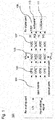
- Fig. 4 shows frequency and impulse response of raised-cosine filter with various roll-off factors. Minimum signal bandwidth is achieved for roll-off factor equal to 0.
- Fig. 5 shows a quadrature phase-shift keying (QPSK) timing error detector characteristic (TEDC) for ROF from 0 to 1 with a step width of 0.1.
- QPSK quadrature phase-shift keying
- TDC timing error detector characteristic
- Fig. 7 shows signal pre-processing.
- power operation in PAM systems is used to generate the clock tone at Baud rate.
- This approach uses specific pre-filter and narrowband filter to filter out the clock tone. It enables the clock extraction for small ROF values but fails for higher ROF values.
- the complete system is realized in the analog domain where is no limitation in terms of sampling frequency and signal digitalizing before the clock extraction.
- the invention describes a method for the clock extraction in Nyquist systems with the benefits that the method enables clock extraction independently on ROF value unlike other known techniques. While present PD detectors often use two complex multiplications per symbol, the proposed PD uses additionally 1.5 complex multiplications per symbol, i.e. totally 3.5 multiplications. The method is independent from the order of QAM and PSK modulation formats and can tolerate a large frequency offset.
- the enhanced PD works with complex modulation formats.
- the received signal is twice over-sampled, ie two samples per symbol.
- samples within one symbol interval n by A(n) and B(n).
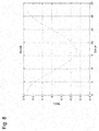
- the TEDC has a sinusoidal shape with positive zero crossing indicating steady-state (sampling instant; see Fig. 8 ).
- Using imaginary part in equation (5) results in TEDC having the constant value over one unit interval (UI) symbol interval. Such a TEDC cannot be used for clock extraction.
- jitter performance is investigated.
- Each TEDC curve is derived on 512 symbols. 64 curves are shown in each figure.
- the amount of jitter can be estimated from the width of positive zero crossing area. In all cases the peak-to-peak jitter does not cross 4% of UI (sampling period; unit interval).
- the frequency offset varies from 0 to 1 GHz in step of 100MHz.
- Baud rate is 28GB.
- Fig. 12 results indicate immunity with respect to a large frequency offset. Even a frequency offset of 1 GHz does not influence TEDC, i.e. the curve with smallest maximum absolute value.
- Fig. 13 shows Nyquist super-channel clocking.
- coherent optical communication spectral efficiency is increased using higher modulation formats, both polarizations and dense channel packaging, like OFDM, Nyquist, etc.
- a group of N transmitters is integrated to save power, size and price.
- a super-channel can share one VCO for all transmitters.
- one VCO supplies the clock distribution unit (CDU) that clocks all N transmitters.
- the receiver side gains from channel integration. Instead of the number of N only one PD is implemented to support clock extraction.
- One PD connected to data of the first receiver or any other receiver extracts clock tone information that is later filtered by low-pass filter (LPF) and sent to VCO.
- LPF low-pass filter
- Fig. 14 shows a parallel implementation of a timing recovery apparatus.
- the timing recovery apparatus comprises a grouper 1401 for grouping digital signal values of a digital signal to obtain groups of values, each group of values comprising a first digital value and a second digital value; a multiplier 1403 for multiplying a first digital value with a conjugated version of a second digital value of each group of values to obtain a first group value representing each group of values, and for multiplying a second digital value of each group of values with a conjugated version of a first digital value of a respectively adjacent group of values to respectively obtain a second group value representing adjacent group of values; a processor 1405 for respectively processing first group values respectively representing adjacent groups of values and a second group values representing the adjacent groups of values to obtain a plurality of processed values; and an averager for determining an average value from the plurality of processed values.
- Maximum number of PD outputs per data block is equal to N. As shown in Fig. 14 , the last output requires first two samples from next data block. In real applications, not all data have to be processed by PDs. Usually, some portion of data are unused that might sacrifice clock performance. High modulation formats require higher signal-to-noise ratios, and the reducing the number of data to be processed in the clock extraction engine does not significantly influence timing performance.
- PD outputs denoted by v are summed up and filtered by a loop filter (low-pass filter) 1407 that can have a proportional-integral structure.
- Filter 1407 outputs control VCO frequency and phase. The VCO output then clocks the subsequent ADC circuit.
- Fig. 15 shows an example timing recovery method, wherein digital signal values of a digital signal are grouped 1501 to obtain groups of values, each group of values comprising a first digital value and a second digital value. Then a first digital value is multiplied 1503 with a conjugated version of a second digital value of each group of values to obtain a first group value representing each group of values, and a second digital value of each group of values is multiplied with a conjugated version of a first digital value of a respectively adjacent group of values to respectively obtain a second group value representing adjacent group of values. Moreover, first group values respectively representing adjacent groups of values and a second group values representing the adjacent groups of values are processed 1505 to obtain a plurality of processed values. Further, an average value is determined 1507 from the plurality of processed values.
- a timing recovery apparatus embodiment which comprises a processor configured to perform the method embodiment as shown in Fig. 15 .
Claims (14)
- Timing-Wiedergewinnungsvorrichtung, umfassend:einen Gruppierer (1401), ausgelegt zum Gruppieren von digitalen Signalwerten eines digitalen Signals, um Gruppen von Werten zu erhalten, wobei jede Gruppe von Werten einen ersten digitalen Wert und einen zweiten digitalen Wert umfasst;einen Multiplizierer (1403), ausgelegt zum Multiplizieren eines ersten digitalen Werts a1, a2, ..., an mit der konjugierten Version eines zweiten digitalen Werts b1*, b2*, ..., bn* jeder Gruppe von Werten, um einen ersten Gruppenwert a1b1 *, a2b2 *, ..., anbn * zu erhalten, der jede Gruppe von Werten repräsentiert, und ausgelegt zum Multiplizieren eines zweiten digitalen Werts b1, b2, ..., bn-1 jeder Gruppe von Werten a1b1, a2b2, ..., anbn, mit der konjugierten Version eines ersten digitalen Werts a2 *, a3 *, ..., an * einer jeweils angrenzenden Gruppe von Werten, um jeweils einen zweiten Gruppenwert b1a2 *, b2a3 *, bn-1an *, der angrenzende Gruppe von Werten repräsentiert, zu erhalten;einen Prozessor (1405), ausgelegt zum Verarbeiten der ersten Gruppenwerte a1b1 *, a2b2 *, ..., anbn *, die jeweils angrenzende Gruppen von Werten repräsentieren, und der zweiten Gruppenwerte b1a2 *, b2a3 *, ..., bn-1an *, die jeweils angrenzende Gruppen von Werten repräsentieren, um mehrere verarbeitete Werte zu erhalten; undeinen Mitteller (1405), ausgelegt zum Bestimmen eines Mittelwerts aus den mehreren verarbeiteten Werten.
- Timing-Wiedergewinnungsvorrichtung nach Anspruch 1, wobei der Gruppierer (1401) ausgelegt ist zum Gruppieren von nachfolgenden N Werten des digitalen Signals, um eine jeweilige Gruppe von Werten zu erhalten.
- Timing-Wiedergewinnungsvorrichtung nach Anspruch 1 oder 2, wobei der Gruppierer (1401) einen Überabtaster umfasst, ausgelegt zum Überabtasten eines eingegebenen optischen Signals, um das digitale Signal zu erhalten.
- Timing-Wiedergewinnungsvorrichtung nach einem der vorhergehenden Ansprüche, wobei der Multiplizierer (1403) mehrere digitale Multiplizierer umfasst.
- Timing-Wiedergewinnungsvorrichtung nach einem der vorhergehenden Ansprüche, wobei der Prozessor (1405) für jede Gruppe von Werten Folgendes umfasst: einen Subtrahierer, ausgelegt zum Subtrahieren von ersten Gruppenwerten, die angrenzende Gruppen von Werten repräsentieren, und einen Multiplizierer, ausgelegt zum Multiplizieren des Subtraktionsergebnisses mit einer jeweiligen zweiten Gruppe von Werten, die diese angrenzende Gruppe von Werten repräsentieren.
- Timing-Wiedergewinnungsvorrichtung nach einem der vorhergehenden Ansprüche, wobei der Mitteller (1405) ausgelegt ist zum Mitteln über Realteile der mehreren verarbeiteten Werte, um den Mittelwert zu bestimmen.
- Timing-Wiedergewinnungsvorrichtung nach einem der vorhergehenden Ansprüche, die ferner ein Schleifenfilter (1407) umfasst, dass dafür ausgelegt ist, den Mittelwert zu filtern.
- Kommunikationsempfängervorrichtung, umfassend:einen Empfänger, ausgelegt zum Empfangen eines Kommunikationssignals;die Timing-Wiedergewinnungsvorrichtung nach einem der vorhergehenden Ansprüche, ausgelegt zur Timing-Wiedergewinnung auf der Basis des Kommunikationssignals; undeinen spannungsgesteuerten Oszillator, ausgelegt zum Bereitstellen eines Taktsignals, wobei dieser spannungsgesteuerte Oszillator durch eine Ausgabe der Wiedergewinnungsvorrichtung gesteuert wird.
- Kommunikationsempfängervorrichtung nach Anspruch 8, wobei das Taktsignal dem Empfänger bereitgestellt wird.
- Kommunikationsempfängervorrichtung nach Anspruch 8 oder 9, die mehrere Empfänger umfasst, wobei das Taktsignal an die mehreren Empfänger verteilt wird.
- Kommunikationsempfängervorrichtung nach Anspruch 8 oder 10, die ferner eine downstream des spannungsgesteuerten Oszillators angeordnete Einheit zur Kompensation chromatischer Dispersion umfasst.
- Timing-Wiedergewinnungsverfahren, umfassend:Gruppieren (1501) von digitalen Signalwerten eines digitalen Signals, um Gruppen von Werten zu erhalten, wobei jede Gruppe von Werten einen ersten digitalen Wert und einen zweiten digitalen Wert umfasst;Multiplizieren (1503) eines ersten digitalen Werts a1, a2, ..., an mit der konjugierten Version eines zweiten digitalen Werts b1*, b2*, ..., bn* jeder Gruppe von Werten, um einen ersten Gruppenwert a1b1 *, a2b2 *, ..., anbn * zu erhalten,der jede Gruppe von Werten repräsentiert, und einen zweiten digitalen Wert b1, b2, ..., bn jeder Gruppe von Werten mit der konjugierten Version eines ersten digitalen Werts a2 *, a3 *, ..., an * einer jeweils angrenzenden Gruppe von Werten multipliziert, um jeweils einen zweiten Gruppenwert, der angrenzende Gruppe von Werten b1a2 *, b2a3 *, ..., bn-1an * repräsentiert, zu erhalten;Verarbeiten (1505) der ersten Gruppenwerte a1b1 *, a2b2 *, ..., anbn *, die jeweils angrenzende Gruppen von Werten repräsentieren, und der zweiten Gruppenwerte b1a2 *, b2a3 *, ..., bn-1an *,Repräsentieren angrenzender Gruppen von Werten, um mehrere verarbeitete Werte zu erhalten; undBestimmen (1507) eines Mittelwerts aus den mehreren verarbeiteten Werten.
- Verfahren zum Erzeugen eines Taktsignals aus einem empfangenen Kommunikationssignal, wobei das Verfahren Folgendes umfasst:Ausführen des Timing-Wiedergewinnungsverfahrens nach Anspruch 12, um Mittelwerte bereitzustellen; undSteuern der Mittelwerte, um das Taktsignal zu erhalten.
- Computerprogramm mit einem Programmcode zum Ausführen des Verfahrens nach Anspruch 12 oder 13, wenn es auf einem Computer laufengelassen wird.
Applications Claiming Priority (1)
| Application Number | Priority Date | Filing Date | Title |
|---|---|---|---|
| PCT/EP2013/055816 WO2014146708A1 (en) | 2013-03-20 | 2013-03-20 | Timing recovery apparatus |
Publications (2)
| Publication Number | Publication Date |
|---|---|
| EP2976852A1 EP2976852A1 (de) | 2016-01-27 |
| EP2976852B1 true EP2976852B1 (de) | 2017-10-25 |
Family
ID=47998418
Family Applications (1)
| Application Number | Title | Priority Date | Filing Date |
|---|---|---|---|
| EP13712521.7A Active EP2976852B1 (de) | 2013-03-20 | 2013-03-20 | Taktrückgewinnungsvorrichtung |
Country Status (3)
| Country | Link |
|---|---|
| EP (1) | EP2976852B1 (de) |
| CN (1) | CN105308895B (de) |
| WO (1) | WO2014146708A1 (de) |
Families Citing this family (1)
| Publication number | Priority date | Publication date | Assignee | Title |
|---|---|---|---|---|
| WO2020094232A1 (en) * | 2018-11-08 | 2020-05-14 | Huawei Technologies Co., Ltd. | Clock extraction in systems affected by strong intersymbol interference |
Family Cites Families (6)
| Publication number | Priority date | Publication date | Assignee | Title |
|---|---|---|---|---|
| JPH05136775A (ja) * | 1991-11-12 | 1993-06-01 | Hitachi Ltd | 多段再生中継システム |
| US7106818B2 (en) * | 2000-10-17 | 2006-09-12 | Koninkijke Philips Electronics N.V. | Method and apparatus for timing recovery based on dispersion characterization and components therefor |
| US7627252B2 (en) * | 2005-02-28 | 2009-12-01 | Nortel Networks Limited | Clock recovery from an optical signal with dispersion impairments |
| US8655191B2 (en) * | 2009-06-29 | 2014-02-18 | Alcatel Lucent | Symbol timing recovery in polarization division multiplexed coherent optical transmission system |
| CN101610108B (zh) * | 2009-07-15 | 2012-07-04 | 电信科学技术第一研究所 | 改善数字扩频接收机载波相位抖动和波形畸变的方法 |
| US8774644B2 (en) * | 2011-02-28 | 2014-07-08 | Infinera Corporation | PMD and chromatic dispersion tolerant clock recovery |
-
2013
- 2013-03-20 CN CN201380074690.9A patent/CN105308895B/zh active Active
- 2013-03-20 WO PCT/EP2013/055816 patent/WO2014146708A1/en active Application Filing
- 2013-03-20 EP EP13712521.7A patent/EP2976852B1/de active Active
Non-Patent Citations (1)
| Title |
|---|
| None * |
Also Published As
| Publication number | Publication date |
|---|---|
| CN105308895A (zh) | 2016-02-03 |
| WO2014146708A1 (en) | 2014-09-25 |
| EP2976852A1 (de) | 2016-01-27 |
| CN105308895B (zh) | 2018-11-13 |
Similar Documents
| Publication | Publication Date | Title |
|---|---|---|
| CN104969524B (zh) | 光传输系统、相位补偿方法以及光接收装置 | |
| JP5163454B2 (ja) | デジタルコヒーレント光受信器において使用される周波数オフセット検出装置および検出方法 | |
| US8655191B2 (en) | Symbol timing recovery in polarization division multiplexed coherent optical transmission system | |
| US8873968B2 (en) | Optical field receiver, optical multilevel signal receiver, and optical transmission system | |
| CN109314572B (zh) | 传输特性补偿装置、传输特性补偿方法以及通信装置 | |
| US8989593B2 (en) | Frequency domain clock recovery | |
| EP2502364B1 (de) | Neigungsmessgerät, neigungskompensator und kohärenter empfänger | |
| CN105393487B (zh) | 相干光接收器 | |
| EP2532107B1 (de) | Taktwiederherstellungsverfahren und taktwiederherstellungsanordung für multiplex-empfänger mit kohärenter polarisation | |
| EP2583424B1 (de) | Verfahren zur messung einer phasen- und oszillatorfrequenz | |
| US9059889B2 (en) | Polar multi-symbol delay detector for carrier phase and frequency recovery for coherent transmission | |
| CN105612700B (zh) | 用于表征光接收信号的色度色散的装置 | |
| JP5316736B1 (ja) | デジタル受信機及び波形補償方法 | |
| JP5921757B2 (ja) | 超高密度wdmシステムのためのクロックリカバリ法 | |
| WO2010094339A1 (en) | Equaliser for an optical transmission system | |
| Baeuerle et al. | Low-complexity real-time receiver for coherent Nyquist-FDM signals | |
| US20210109563A1 (en) | Clock phase detection using interior spectral components | |
| CN107395287B (zh) | 一种频偏估计方法和装置 | |
| JPWO2015025468A1 (ja) | 周波数偏差補償方式、周波数偏差補償方法及びプログラム | |
| US11502756B2 (en) | Data synchronization in optical networks and devices | |
| EP2976852B1 (de) | Taktrückgewinnungsvorrichtung | |
| Payyazhi et al. | Recursive blind phase search architecture for phase recovery at high error rates | |
| CN111869157B (zh) | 用于数据传输系统中的定时恢复装置和定时恢复方法 | |
| CN114726450B (zh) | 一种色散容忍的时钟恢复方法及系统 | |
| EP3433952B1 (de) | Taktrückgewinnungsvorrichtung und -verfahren in direktdetektionsempfängern |
Legal Events
| Date | Code | Title | Description |
|---|---|---|---|
| PUAI | Public reference made under article 153(3) epc to a published international application that has entered the european phase |
Free format text: ORIGINAL CODE: 0009012 |
|
| 17P | Request for examination filed |
Effective date: 20151020 |
|
| AK | Designated contracting states |
Kind code of ref document: A1 Designated state(s): AL AT BE BG CH CY CZ DE DK EE ES FI FR GB GR HR HU IE IS IT LI LT LU LV MC MK MT NL NO PL PT RO RS SE SI SK SM TR |
|
| AX | Request for extension of the european patent |
Extension state: BA ME |
|
| DAX | Request for extension of the european patent (deleted) | ||
| 17Q | First examination report despatched |
Effective date: 20160928 |
|
| GRAP | Despatch of communication of intention to grant a patent |
Free format text: ORIGINAL CODE: EPIDOSNIGR1 |
|
| INTG | Intention to grant announced |
Effective date: 20170220 |
|
| GRAS | Grant fee paid |
Free format text: ORIGINAL CODE: EPIDOSNIGR3 |
|
| GRAJ | Information related to disapproval of communication of intention to grant by the applicant or resumption of examination proceedings by the epo deleted |
Free format text: ORIGINAL CODE: EPIDOSDIGR1 |
|
| GRAL | Information related to payment of fee for publishing/printing deleted |
Free format text: ORIGINAL CODE: EPIDOSDIGR3 |
|
| INTC | Intention to grant announced (deleted) | ||
| GRAR | Information related to intention to grant a patent recorded |
Free format text: ORIGINAL CODE: EPIDOSNIGR71 |
|
| GRAA | (expected) grant |
Free format text: ORIGINAL CODE: 0009210 |
|
| AK | Designated contracting states |
Kind code of ref document: B1 Designated state(s): AL AT BE BG CH CY CZ DE DK EE ES FI FR GB GR HR HU IE IS IT LI LT LU LV MC MK MT NL NO PL PT RO RS SE SI SK SM TR |
|
| INTG | Intention to grant announced |
Effective date: 20170915 |
|
| REG | Reference to a national code |
Ref country code: GB Ref legal event code: FG4D |
|
| REG | Reference to a national code |
Ref country code: CH Ref legal event code: EP |
|
| REG | Reference to a national code |
Ref country code: AT Ref legal event code: REF Ref document number: 940839 Country of ref document: AT Kind code of ref document: T Effective date: 20171115 |
|
| REG | Reference to a national code |
Ref country code: IE Ref legal event code: FG4D |
|
| REG | Reference to a national code |
Ref country code: DE Ref legal event code: R096 Ref document number: 602013028365 Country of ref document: DE |
|
| REG | Reference to a national code |
Ref country code: FR Ref legal event code: PLFP Year of fee payment: 6 |
|
| REG | Reference to a national code |
Ref country code: NL Ref legal event code: MP Effective date: 20171025 |
|
| REG | Reference to a national code |
Ref country code: LT Ref legal event code: MG4D |
|
| REG | Reference to a national code |
Ref country code: AT Ref legal event code: MK05 Ref document number: 940839 Country of ref document: AT Kind code of ref document: T Effective date: 20171025 |
|
| PG25 | Lapsed in a contracting state [announced via postgrant information from national office to epo] |
Ref country code: NL Free format text: LAPSE BECAUSE OF FAILURE TO SUBMIT A TRANSLATION OF THE DESCRIPTION OR TO PAY THE FEE WITHIN THE PRESCRIBED TIME-LIMIT Effective date: 20171025 |
|
| PG25 | Lapsed in a contracting state [announced via postgrant information from national office to epo] |
Ref country code: FI Free format text: LAPSE BECAUSE OF FAILURE TO SUBMIT A TRANSLATION OF THE DESCRIPTION OR TO PAY THE FEE WITHIN THE PRESCRIBED TIME-LIMIT Effective date: 20171025 Ref country code: ES Free format text: LAPSE BECAUSE OF FAILURE TO SUBMIT A TRANSLATION OF THE DESCRIPTION OR TO PAY THE FEE WITHIN THE PRESCRIBED TIME-LIMIT Effective date: 20171025 Ref country code: SE Free format text: LAPSE BECAUSE OF FAILURE TO SUBMIT A TRANSLATION OF THE DESCRIPTION OR TO PAY THE FEE WITHIN THE PRESCRIBED TIME-LIMIT Effective date: 20171025 Ref country code: LT Free format text: LAPSE BECAUSE OF FAILURE TO SUBMIT A TRANSLATION OF THE DESCRIPTION OR TO PAY THE FEE WITHIN THE PRESCRIBED TIME-LIMIT Effective date: 20171025 Ref country code: NO Free format text: LAPSE BECAUSE OF FAILURE TO SUBMIT A TRANSLATION OF THE DESCRIPTION OR TO PAY THE FEE WITHIN THE PRESCRIBED TIME-LIMIT Effective date: 20180125 |
|
| PG25 | Lapsed in a contracting state [announced via postgrant information from national office to epo] |
Ref country code: AT Free format text: LAPSE BECAUSE OF FAILURE TO SUBMIT A TRANSLATION OF THE DESCRIPTION OR TO PAY THE FEE WITHIN THE PRESCRIBED TIME-LIMIT Effective date: 20171025 Ref country code: IS Free format text: LAPSE BECAUSE OF FAILURE TO SUBMIT A TRANSLATION OF THE DESCRIPTION OR TO PAY THE FEE WITHIN THE PRESCRIBED TIME-LIMIT Effective date: 20180225 Ref country code: LV Free format text: LAPSE BECAUSE OF FAILURE TO SUBMIT A TRANSLATION OF THE DESCRIPTION OR TO PAY THE FEE WITHIN THE PRESCRIBED TIME-LIMIT Effective date: 20171025 Ref country code: HR Free format text: LAPSE BECAUSE OF FAILURE TO SUBMIT A TRANSLATION OF THE DESCRIPTION OR TO PAY THE FEE WITHIN THE PRESCRIBED TIME-LIMIT Effective date: 20171025 Ref country code: BG Free format text: LAPSE BECAUSE OF FAILURE TO SUBMIT A TRANSLATION OF THE DESCRIPTION OR TO PAY THE FEE WITHIN THE PRESCRIBED TIME-LIMIT Effective date: 20180125 Ref country code: RS Free format text: LAPSE BECAUSE OF FAILURE TO SUBMIT A TRANSLATION OF THE DESCRIPTION OR TO PAY THE FEE WITHIN THE PRESCRIBED TIME-LIMIT Effective date: 20171025 Ref country code: GR Free format text: LAPSE BECAUSE OF FAILURE TO SUBMIT A TRANSLATION OF THE DESCRIPTION OR TO PAY THE FEE WITHIN THE PRESCRIBED TIME-LIMIT Effective date: 20180126 |
|
| REG | Reference to a national code |
Ref country code: DE Ref legal event code: R097 Ref document number: 602013028365 Country of ref document: DE |
|
| PG25 | Lapsed in a contracting state [announced via postgrant information from national office to epo] |
Ref country code: DK Free format text: LAPSE BECAUSE OF FAILURE TO SUBMIT A TRANSLATION OF THE DESCRIPTION OR TO PAY THE FEE WITHIN THE PRESCRIBED TIME-LIMIT Effective date: 20171025 Ref country code: CY Free format text: LAPSE BECAUSE OF FAILURE TO SUBMIT A TRANSLATION OF THE DESCRIPTION OR TO PAY THE FEE WITHIN THE PRESCRIBED TIME-LIMIT Effective date: 20171025 Ref country code: EE Free format text: LAPSE BECAUSE OF FAILURE TO SUBMIT A TRANSLATION OF THE DESCRIPTION OR TO PAY THE FEE WITHIN THE PRESCRIBED TIME-LIMIT Effective date: 20171025 Ref country code: SK Free format text: LAPSE BECAUSE OF FAILURE TO SUBMIT A TRANSLATION OF THE DESCRIPTION OR TO PAY THE FEE WITHIN THE PRESCRIBED TIME-LIMIT Effective date: 20171025 Ref country code: CZ Free format text: LAPSE BECAUSE OF FAILURE TO SUBMIT A TRANSLATION OF THE DESCRIPTION OR TO PAY THE FEE WITHIN THE PRESCRIBED TIME-LIMIT Effective date: 20171025 |
|
| PG25 | Lapsed in a contracting state [announced via postgrant information from national office to epo] |
Ref country code: PL Free format text: LAPSE BECAUSE OF FAILURE TO SUBMIT A TRANSLATION OF THE DESCRIPTION OR TO PAY THE FEE WITHIN THE PRESCRIBED TIME-LIMIT Effective date: 20171025 Ref country code: SM Free format text: LAPSE BECAUSE OF FAILURE TO SUBMIT A TRANSLATION OF THE DESCRIPTION OR TO PAY THE FEE WITHIN THE PRESCRIBED TIME-LIMIT Effective date: 20171025 Ref country code: IT Free format text: LAPSE BECAUSE OF FAILURE TO SUBMIT A TRANSLATION OF THE DESCRIPTION OR TO PAY THE FEE WITHIN THE PRESCRIBED TIME-LIMIT Effective date: 20171025 Ref country code: RO Free format text: LAPSE BECAUSE OF FAILURE TO SUBMIT A TRANSLATION OF THE DESCRIPTION OR TO PAY THE FEE WITHIN THE PRESCRIBED TIME-LIMIT Effective date: 20171025 |
|
| PLBE | No opposition filed within time limit |
Free format text: ORIGINAL CODE: 0009261 |
|
| STAA | Information on the status of an ep patent application or granted ep patent |
Free format text: STATUS: NO OPPOSITION FILED WITHIN TIME LIMIT |
|
| 26N | No opposition filed |
Effective date: 20180726 |
|
| REG | Reference to a national code |
Ref country code: CH Ref legal event code: PL |
|
| PG25 | Lapsed in a contracting state [announced via postgrant information from national office to epo] |
Ref country code: MC Free format text: LAPSE BECAUSE OF FAILURE TO SUBMIT A TRANSLATION OF THE DESCRIPTION OR TO PAY THE FEE WITHIN THE PRESCRIBED TIME-LIMIT Effective date: 20171025 Ref country code: SI Free format text: LAPSE BECAUSE OF FAILURE TO SUBMIT A TRANSLATION OF THE DESCRIPTION OR TO PAY THE FEE WITHIN THE PRESCRIBED TIME-LIMIT Effective date: 20171025 |
|
| REG | Reference to a national code |
Ref country code: BE Ref legal event code: MM Effective date: 20180331 |
|
| REG | Reference to a national code |
Ref country code: IE Ref legal event code: MM4A |
|
| PG25 | Lapsed in a contracting state [announced via postgrant information from national office to epo] |
Ref country code: LU Free format text: LAPSE BECAUSE OF NON-PAYMENT OF DUE FEES Effective date: 20180320 |
|
| PG25 | Lapsed in a contracting state [announced via postgrant information from national office to epo] |
Ref country code: IE Free format text: LAPSE BECAUSE OF NON-PAYMENT OF DUE FEES Effective date: 20180320 |
|
| PG25 | Lapsed in a contracting state [announced via postgrant information from national office to epo] |
Ref country code: CH Free format text: LAPSE BECAUSE OF NON-PAYMENT OF DUE FEES Effective date: 20180331 Ref country code: LI Free format text: LAPSE BECAUSE OF NON-PAYMENT OF DUE FEES Effective date: 20180331 Ref country code: BE Free format text: LAPSE BECAUSE OF NON-PAYMENT OF DUE FEES Effective date: 20180331 |
|
| PG25 | Lapsed in a contracting state [announced via postgrant information from national office to epo] |
Ref country code: MT Free format text: LAPSE BECAUSE OF NON-PAYMENT OF DUE FEES Effective date: 20180320 |
|
| PG25 | Lapsed in a contracting state [announced via postgrant information from national office to epo] |
Ref country code: TR Free format text: LAPSE BECAUSE OF FAILURE TO SUBMIT A TRANSLATION OF THE DESCRIPTION OR TO PAY THE FEE WITHIN THE PRESCRIBED TIME-LIMIT Effective date: 20171025 |
|
| PG25 | Lapsed in a contracting state [announced via postgrant information from national office to epo] |
Ref country code: PT Free format text: LAPSE BECAUSE OF FAILURE TO SUBMIT A TRANSLATION OF THE DESCRIPTION OR TO PAY THE FEE WITHIN THE PRESCRIBED TIME-LIMIT Effective date: 20171025 |
|
| PG25 | Lapsed in a contracting state [announced via postgrant information from national office to epo] |
Ref country code: MK Free format text: LAPSE BECAUSE OF NON-PAYMENT OF DUE FEES Effective date: 20171025 Ref country code: HU Free format text: LAPSE BECAUSE OF FAILURE TO SUBMIT A TRANSLATION OF THE DESCRIPTION OR TO PAY THE FEE WITHIN THE PRESCRIBED TIME-LIMIT; INVALID AB INITIO Effective date: 20130320 |
|
| PG25 | Lapsed in a contracting state [announced via postgrant information from national office to epo] |
Ref country code: AL Free format text: LAPSE BECAUSE OF FAILURE TO SUBMIT A TRANSLATION OF THE DESCRIPTION OR TO PAY THE FEE WITHIN THE PRESCRIBED TIME-LIMIT Effective date: 20171025 |
|
| PGFP | Annual fee paid to national office [announced via postgrant information from national office to epo] |
Ref country code: FR Payment date: 20230208 Year of fee payment: 11 |
|
| PGFP | Annual fee paid to national office [announced via postgrant information from national office to epo] |
Ref country code: DE Payment date: 20240130 Year of fee payment: 12 Ref country code: GB Payment date: 20240201 Year of fee payment: 12 |