EP2976707B1 - Dispositif et procédé pour générer des bits aléatoires - Google Patents
Dispositif et procédé pour générer des bits aléatoires Download PDFInfo
- Publication number
- EP2976707B1 EP2976707B1 EP14707725.9A EP14707725A EP2976707B1 EP 2976707 B1 EP2976707 B1 EP 2976707B1 EP 14707725 A EP14707725 A EP 14707725A EP 2976707 B1 EP2976707 B1 EP 2976707B1
- Authority
- EP
- European Patent Office
- Prior art keywords
- mapping
- combinatorial
- signal
- signals
- input
- Prior art date
- Legal status (The legal status is an assumption and is not a legal conclusion. Google has not performed a legal analysis and makes no representation as to the accuracy of the status listed.)
- Not-in-force
Links
Images


Classifications
-
- G—PHYSICS
- G06—COMPUTING; CALCULATING OR COUNTING
- G06F—ELECTRIC DIGITAL DATA PROCESSING
- G06F7/00—Methods or arrangements for processing data by operating upon the order or content of the data handled
- G06F7/58—Random or pseudo-random number generators
- G06F7/588—Random number generators, i.e. based on natural stochastic processes
-
- H—ELECTRICITY
- H03—ELECTRONIC CIRCUITRY
- H03K—PULSE TECHNIQUE
- H03K3/00—Circuits for generating electric pulses; Monostable, bistable or multistable circuits
- H03K3/84—Generating pulses having a predetermined statistical distribution of a parameter, e.g. random pulse generators
-
- H—ELECTRICITY
- H04—ELECTRIC COMMUNICATION TECHNIQUE
- H04L—TRANSMISSION OF DIGITAL INFORMATION, e.g. TELEGRAPHIC COMMUNICATION
- H04L9/00—Cryptographic mechanisms or cryptographic arrangements for secret or secure communications; Network security protocols
- H04L9/06—Cryptographic mechanisms or cryptographic arrangements for secret or secure communications; Network security protocols the encryption apparatus using shift registers or memories for block-wise or stream coding, e.g. DES systems or RC4; Hash functions; Pseudorandom sequence generators
- H04L9/065—Encryption by serially and continuously modifying data stream elements, e.g. stream cipher systems, RC4, SEAL or A5/3
- H04L9/0656—Pseudorandom key sequence combined element-for-element with data sequence, e.g. one-time-pad [OTP] or Vernam's cipher
-
- H—ELECTRICITY
- H04—ELECTRIC COMMUNICATION TECHNIQUE
- H04L—TRANSMISSION OF DIGITAL INFORMATION, e.g. TELEGRAPHIC COMMUNICATION
- H04L9/00—Cryptographic mechanisms or cryptographic arrangements for secret or secure communications; Network security protocols
- H04L9/08—Key distribution or management, e.g. generation, sharing or updating, of cryptographic keys or passwords
- H04L9/0861—Generation of secret information including derivation or calculation of cryptographic keys or passwords
- H04L9/0866—Generation of secret information including derivation or calculation of cryptographic keys or passwords involving user or device identifiers, e.g. serial number, physical or biometrical information, DNA, hand-signature or measurable physical characteristics
Definitions
- the present invention relates to an apparatus and method for generating one or more random bits. For example, a random bit sequence is generated which is used as a binary random number.
- the proposed devices and methods for generating random bits serve, for example, the implementation of random number generators.
- random bit sequences are necessary as binary random numbers. It is desired, in particular for mobile applications to operate as little hardware as possible.
- Known measures for generating random numbers are, for example, pseudo-random numbers, analogue random sources, ring oscillators and their modifications.
- pseudo-random numbers seeds are used, from which deterministic pseudorandom numbers are calculated.
- a physical random number generator is usually used.
- analog random sources noise sources such as e.g. the noise of zener diodes, amplified and digitized.
- the connection between digital and analog circuit technology is usually difficult to realize.
- ring oscillators which are made up of an odd number of inverters connected in series
- random jitter results from fluctuating throughput times of the signals through the inverters.
- These jitter that is, an irregular variation with time in state changes of the signals sent by the inverters, can be accumulated in multiple passes through the ring oscillator circuit, so that ultimately a random analog signal arises.
- a disadvantage of ring oscillators is often the necessary long time from the start of the oscillation until a usable random signal due to the jitter accumulation arises. Therefore, mostly low unacceptable data generation rates arise for ring oscillators. It is also possible that the adding jitter contributions also cancel themselves out, so that on average random short gate delays are compensated by random longer gate delays.
- Fibonacci and Galois ring oscillators generate random waveforms faster than classical ring oscillators.
- various digital gates such as XOR and NOT gates are used. This can result in particular in implementations on ASICs large speed differences of the gate types.
- FPGAs Field Programmable Gate Arrays
- EP 1 643 643 A1 discloses a random number generator with two ring oscillators, wherein feedback from an external parity signal is provided.
- an apparatus for generating random bits which comprises: a plurality of imaging devices, wherein a respective imaging device is set up to image a predetermined number n of input signals into a predefined number p of output signals by means of a combinatorial mapping.
- the imaging devices concatenated with each other, and at least one feedback loop is formed.
- the feedback loop is in particular designed such that a change in state of at least one output signal of a selected imaging device as a change in state at least an input signal is fed to another imaging device.
- the other imaging device is not a directly adjacent imaging device.
- a feedback loop is provided in such a way that a state change of at least one feedback output signal of a specific imaging device is supplied as a change in state of at least one input signal of another imaging device such that one or more output signals of the particular imaging device is influenced by the state change of the feedback output signal.
- At least one combinatorial mapping is set up in such a way that a state change of an input signal of a respective imaging device is mapped on average to more than one output signal of the respective imaging device.
- the number of n input signals of a respective imaging device may correspond to the number p of the output signals.
- n is not equal to p, ie that with the aid of a respective imaging device, the states of the input signals are mapped to states of output signals, wherein the number of output signals is smaller or larger than the number of input signals for a respective imaging device.
- the imaging devices may be logic or combinatorial gates, which in particular realize a bijective mapping of n input signals to n output signals.
- the input signals fluctuate between levels that can be assigned to logic states such as bits 1 or high or 0 or low.
- a bijective mapping is a one-to-one mapping between the 2 n possible logical values of the input signals and the 2 n logic values of the output signals.
- an n-track ring oscillator results with the aid of the imaging devices in embodiments of the device.
- the imaging devices may also be referred to as nodes or gates.
- the respective combinatorial mapping is set up in particular in such a way that, on average, a state change ensues on a change of state of an input signal at more than one output signal.
- a respective jitter of the input signal is mapped to a plurality of output signals and therefore amplified. Once a jitter has occurred in a signal, it is copied to a plurality of output tracks with the aid of the imaging devices or the combinatorial mappings implemented therein, so that jitter components can hardly be compensated.
- a multi-track ring oscillator circuit in contrast to classical single-track ring oscillators, there is the particular advantage that random bit values can be tapped with a higher data rate.
- a random bit signal may be derived on one or more of the data paths resulting from the n input and output signals.
- the device develops "oscillations" or signal changes propagate in a circle.
- at least one of the outputs causally depends on itself by being fed back, the feedback being done by means of a plurality of interleaved mappings.
- At least one combinatorial mapping is arranged such that the input signals are mapped to the output signals while applying a jitter and a logical function. Due to the hardware implementation of the combinatorial mapping by the imaging devices, jitter, ie fluctuations, can result in the time course of signal edges. This jitter is then completed the logical function, ie the mapping of the combination of n input signals or bit values to n output signals or bit values is continued in each case and accumulates over the passes and feedback of the imaging devices.
- mappings are not combinatorial mappings which exclusively provide a permutation of the input signals to the output signals.
- a permutation of the input signals is present in particular when the output signals correspond to the input signals, or arise only by a change in the order of the input signals. In a permutation there is no "duplication" of the jitter.
- the imaging devices are arranged such that their signal transit times are the same.
- the same signal propagation times reduce the risk that jitter contributions can compensate each other. It also facilitates implementation in the manner of ASICs or FPGAs.
- the mapping means are arranged so that all possible state changes at the respective outputs are all within a tolerance interval of 100 ps and preferably within 50 ps.
- At least one mapping device comprises a lookup table for implementing the combinatorial mapping. It is also possible that all imaging devices are provided with a respective lookup table. Lookup tables can be easily read and require only a small amount of hardware. Frequently in programmable logic chips, such as FPGAs, corresponding fields or already tables are provided.
- the lookup tables may be random bit values using random elements be filled. For example, it is possible to generate the lookup tables that provide a corresponding output bit pattern at outputs in response to an input bit pattern at inputs of the mapping devices such that the representation represented by the lookup table happens to be from all (2 n )! Bijections of n logical signals to n logical signals is selected. Preferably, different combinatorial mappings are implemented in the imaging devices.
- the concatenated imaging devices form a multi-track ring oscillator circuit.
- the device is set up in such a way that the input signals are predetermined in such a way that the device is not present in a fixed point, in particular when the input signals are coupled in for the first time.
- fixed well-defined levels may be applied to the inputs of one of the imaging devices to start from a well-defined state.
- the feedback and the concatenated application of the combinatorial mappings to the signals results in an n or p bit wide random bit signal.
- the device is preferably arranged in particular such that it has no fixed point.
- the combinatorial mappings are selected and implemented in such a way that there is no fixed point.
- the predetermined number n or p of input or output signals is at least three.
- the bit width or the number n or p of predetermined input or Output signals at the imaging devices four or more.
- a scanning device for scanning one or more output signals at outputs of an imaging device.
- the scanning device can also detect a respective input or output signal at different imaging devices.
- the sampling takes place, for example, clocked or at predetermined other times and serves to derive a bit value H or L, which has a high entropy or randomness due to the strongly fluctuating random signal.
- the scanning device comprises at least one buffer element.
- the latching element may comprise a flip-flop, such as a T-flip-flop or a latch device. Also conceivable are one or more counters for detecting signal edges or state changes of individual signals.
- a T-flip-flop is particularly suitable for counting rising or falling signal edges modulo 2.
- the detection device may be configured such that an output signal is sampled in dependence on another output signal. It is conceivable, for example, that a signal edge of a first output signal triggers or causes the sampling of another output signal.
- the device is part of an FPGA device or an ASIC device.
- a method for generating random bits in which a plurality of combinatorial pictures are performed concatenated one after the other.
- a respective combinational image maps a predetermined number n of input signals to a predetermined number p of output signals.
- at least one feedback loop is formed.
- at least one combinatorial image is created chosen such that a change in state of an input signal is mapped by the combinatorial mappings on average to more than one output signal.
- a respective input signal may represent a bit value, for example.
- the at least one feedback is formed in such a way that a change in state of at least one output signal of a selected combinational mapping as a change in state of at least one input signal is fed to another combinatorial mapping.
- the combinatorial mappings can be referred to as n on p mappings.
- the method can in particular be implemented on or in an FPGA or ASIC device via suitable description languages, for example VHDL or Verilog.
- the imaging devices are preferably set up in such a way that state changes on an input signal of the n input signals as a function of the combinatorial mapping cause a state change in one or more of the p output signals at the same time.
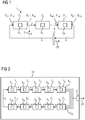
- the Fig. 1 shows a schematic representation of a first embodiment of an apparatus for generating random bits.
- the device 1 is constructed in the manner of an n-channel or n-track ring oscillator.
- combinatorial digital circuits 2 1 to 2 m are serially connected in series.
- the combinatorial digital circuits 2 1 to 2 m can also be understood as logic gates or imaging devices for a respective combinatorial mapping.
- the inputs and outputs are not explicitly indicated.
- a respective imaging device 2 i receives insofar E i1 to E in input signals and outputs A i1 to A ip output signals.
- the connection between input and output signals is over realized a combinational mapping K i .
- n p
- the K 1 to K m combinatorial images are concatenated successively and the imaging result or the output signals A m1 to A mp are performed as input signals E 11 to E 1n to the first imaging device 2 1 .
- a feedback results as in a ring oscillator.
- imaging devices 2 1 - 2 m form an annular topology
- a forward coupling of output signals A m1 to A mn at inputs downstream linkage imaging devices 2 1 - 2 m can cause jittery signal edges propagate through the concatenated imaging devices 2 1 - 2 m while jittering is amplified and multiplied.
- the respective imaging device 2 i with the implemented combinatorial mapping K i can also be referred to as a node, gate or combinatorial digital circuit.
- the imaging devices in the 2 1 to 2 m implemented combinatorial images K 1 to K m are chosen so that a change of a respective input bit or a logical state of an input signal E ij on average leads to changes in more than one of the output bits of the respective node or the respective imaging device.
- jitter that is present in the signals E 11 to E mn or A 11 to A mn accumulates and multiplies when passing through the linked imaging devices 2 1 to 2 m .
- the respective signal transit time in an imaging device or a logic or combinatorial gate 2 i is essentially the same for all input signals E i1 to E in , so that, due to the implemented combinatorial mapping K i, the change of a logic state at an input signal E ij substantially simultaneously to logic changes to one or more output signals A il with l ⁇ ⁇ 1, 2, ... n ⁇ . As such, there are n channels with random waveforms caused by the jitter caused by the switching elements constituting the digital imaging devices.
- a scanning device 4 which detects, for example, one or more of the output signals A m1 to A mn of the imaging device 2 m and, since a random signal waveform results, from which a random bit signal ZB is derived. For example, it is possible to clock or, if required, to pick up and record a signal level and to interpret it as an H or L or 1- or 0-bit value.
- the device or the random bit generator 1 it is possible to put the device or the random bit generator 1 in an initial state in which there is no fixed point. This takes place, for example, by virtue of the fact that, for example, the input signals E 11 to E 1n for the first imaging device 2 1 are given well-defined levels over the entire bit width n.
- the feedback line between the imaging device 2 m and the imaging device 2 1 may be temporarily interrupted. Then let the oscillation run free, so that random signal forms result in the n tapped channels or paths.
- Fig. 1 is optionally indicated that also another feedback path 3 (shown in phantom) can be implemented.
- another feedback path 3 shown in phantom
- the schematically indicated device for generating random bits 1 can be realized, in particular, at low cost in FPGA or ASIC devices. Compared to classical single-channel ring oscillators, random bits can be generated with a higher data rate since, in particular, the randomly favorable jitter is potentially multiplied n times with the aid of the multiple channels. It is unlikely that Jitter's contributions compensate each other because of the many channels and images. In this respect, a random number generator with a high random bit generation frequency can be realized in a cost-effective manner.
- Fig. 2 is a further embodiment of an apparatus for generating random bits indicated.
- the random bit generator 10 is implemented by means of an FPGA chip.
- m 10 combinatorial gates or imaging devices 2 1 to 2 10 connected in series and fed back.
- the combinational gates 2 1 to 2 10 each have four inputs and four outputs, resulting in a four-channel or four-track ring oscillator.
- the combinatorial images, which are realized by the gates 2 1 to 2 10 result from lookup tables 5 1 to 5 10 .
- the input signals E q1 - E q4 and the output signals A q1 - A q4 represent logical states 0 or 1 and L or H, respectively, although due to the "randomness" and heavy application of random jitter there are rather no well defined logic levels in the hardware-implemented circuitry for generating random bits.
- the table can be implemented as a look-up table for forming the mapping device 2q.
- a bijective mapping is implemented so that each possible bit pattern of four input bits or input signal states E q1 , E q2 , E q3 , E q4 occurs exactly once at the outputs of the mapping device 2q as output signal states A q1 , A q2 , A q3 , A q4 .
- An input bit pattern of 0010 results in an output bit pattern 0011 (see third row of the table).
- the signal edges which correspond to the state changes, applied to other jitters and "copied" to several, in the present example to 2.75 output signals.
- a jittery input signal is converted or imaged into a plurality of jittery output signals, additional jitter being supplemented by the respective mapping itself.
- the jitter which is used as a random phenomenon, is thus amplified and distributed over several channels.
- the combinatorial mapping K q represented as an example in tabular form, can be represented equivalently in the form of Boolean functions.
- OR is a logical OR
- AND is a logical AND
- NOT is a logical NOT.
- the combinatorial mappings may be used as a logical gate mappings in place of a lookup table above illustration are realized.
- a q 3 EMERGENCY XOR e q 1 . e q 2 . e q 4 . AND e q 4 e q 2 e q 1 .
- the output signal A q4 is independent of a state change of the input signal E q2 .
- An even more optimized construction of the combinatorial maps K q provides that a respective output signal depends on as many input signals as possible. It would be particularly preferable for each output signal of a combinatorial mapping to be dependent on all input signals for the mapping. Then jitter in the signals would multiply and amplify very well.
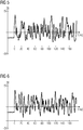
- Fig. 3 to 6 show variants of random bit signals ZB used with an FPGA implementation of the in Fig. 2 are generated circuit shown.
- the y-axis shows the signal level in volts and the x-axis the time in nanoseconds. Random bijective n-to-n bitmaps were used. It can be seen that with the same starting values, even after a short time, for example after 10 ns, completely different signal forms occur, which are random. In this respect, the random waveforms can be used as a basis for determining random bit values.
- the Fig. 7 shows a schematic representation of a third embodiment of an apparatus for generating random bits.
- the device 100 implements several optional modifications of the related art Fig. 1 and 2 Devices 1 and 10 explained.
- the device 100 comprises five imaging devices 2 1 - 2 5 , each implementing a combinatorial mapping K 1 - K 5 .
- the images K 1 and K 5 each represent four input signals to four output signals.
- the imaging devices 2 1 and 2 5 inputs for four input signals E 11 - E 14 and E 51 - E 54 and the same number of outputs for each four output signals A 11 - A 14 and A 51 - A 54th
- the figures K 2 and K 3 form three input signals E 21 , E 22 , E 23 and E 31 , E 32 , E 33 to four output signals A 21 - A 24 and A 31 - A 34 from.
- the map K 4 is a four-by-three map and generates three output signals A 41 , A 42 , A 43 from four input signals E 41 -E 44 .
- the output signal A 23 is fed forward or fed back as input signal E 51 depending on the perspective.
- the output signals A 13 and A 14 are logically rounded by means of an AND gate 11 and supplied as input signal E 23 of the imaging device 2 2 .
- the output signals A 52 and A 53 are logically ORed by means of an OR gate 11, inverted with an inverter 8, and input signal E 11 of the imaging device 2 1 supplied.
- the output signal A 31 is inverted by means of an inverter 6 to the input signal E 44 .
- the maps K 1 - K 5 are arranged so that a change in state of an input signal is mapped on average to more than one output signal.
- a bijective image as explained with respect to the table above can be used.
- a feedback loop results, for example, from the signals A 14 , E 23 , A 23 , E 51 and A 51 , due to the design of the maps K 1 , K 2 and K 5 signal edges are also transferred to other paths in the device 100 and cause random waveforms.
- the signals A 33 and A 54 are each tapped with the aid of toggle flip-flops 9.
- the respective T flip-flop 9 serves as a counter which counts rising signal edges as 0 ⁇ 1 passes modulo 2.
- a respective random bit can be tapped.
- the proposed device and the underlying method are particularly suitable for implementation in ASICs.
- the logical functions of the imaging devices preferably have the same logical depth to achieve the same signal propagation time of the combinatorial mappings.
- lookup tables can also be dispensed with.
- the invention thus enables rapid random bit generation with low hardware expenditure.
Claims (15)
- Entité (1) pour générer des bits aléatoires (ZB), comprenant :plusieurs entités d'application (21 - 2m), une entité d'application respective (21 - 2m) étant configurée pour appliquer un nombre donné n de signaux d'entrée (E11 - Emn) sur un nombre donné p de signaux de sortie (A11 - Amp) à l'aide d'une application combinatoire (K1 - Km), les entités d'application (21 - 2m) étant enchaînées et au moins une boucle de rétroaction étant constituée de telle sorte qu'un changement d'état d'au moins un signal de sortie (Aij) d'une entité d'application (2i) est envoyé en tant que changement d'état d'au moins un signal d'entrée (Ek1) sur une autre entité d'application (2k),
caractérisé en ce queau moins une application combinatoire (K1 - Km) est configurée de telle sorte qu'un changement d'état d'un signal d'entrée (E11 - Emn) d'une entité d'application respective (21 - 2m) est appliqué, en moyenne, sur plus d'un signal de sortie (A11 - Amp) de l'entité d'application respective (21 - 2m). - Entité (1) selon la revendication 1, au moins une application combinatoire (K1 - Km) étant configurée de telle sorte que les signaux d'entrée (E11 - Emn) sont appliqués sur les signaux de sortie (A11 - Amp) avec application d'une gigue et d'une fonction logique.
- Entité (1) selon la revendication 1 ou 2, les applications combinatoires (K1 - Km) n'implémentant pas d'application combinatoire qui fournit une permutation des signaux d'entrée (E11 - Emn) sur les signaux de sortie (A11 - Amp).
- Entité (1) selon l'une des revendications 1 - 3, les entités d'application (21 - 2m) étant configurées de telle sorte que leurs temps de passage des signaux sont identiques.
- Entité (1) selon l'une des revendications 1 - 4, au moins une entité d'application (21 - 2m) comprenant un tableau de consultation (51 - 5m) pour implémenter l'application combinatoire (K1 - Km).
- Entité (1) selon l'une des revendications 1 - 5, au moins une application combinatoire (Kq) correspondant à une bijection.
- Entité (1) selon l'une des revendications 1 - 6, les entités d'application (21 - 2m) implémentant respectivement différentes applications combinatoires (K1 - Km).
- Entité (1) selon l'une des revendications 1 - 7, les entités d'application (21 - 2m) enchaînées formant un oscillateur en anneau à n voies.
- Entité (1) selon l'une des revendications 1 - 8, l'entité comprenant plusieurs branches de rétroaction (3) d'entités d'application enchaînées (21 - 2m).
- Entité (1) selon l'une des revendications 1 - 9, l'entité (1) étant configurée de telle sorte que, lors du couplage de signaux d'entrée donnés (E11 - Emn), les signaux d'entrée donnés (E11 - Emn) sont tels que l'entité (1) ne se trouve pas à un point fixe.
- Entité (1) selon l'une des revendications 1 - 10, comportant en outre un dispositif d'échantillonnage (4) pour échantillonner un ou plusieurs signaux de sortie (A11 - Amp) à des sorties d'une ou de différentes entités d'application (21 - 2m).
- Entité (1) selon la revendication 11, le dispositif d'échantillonnage (4) comportant un élément de stockage intermédiaire, et plus particulièrement une bascule T.
- Dispositif FPGA ou dispositif ASIC comportant une entité selon l'une des revendications 1 - 12.
- Procédé pour générer des bits aléatoires (ZB), dans lequel plusieurs applications combinatoires (K1 - Km) sont effectuées successivement de manière enchaînée, une application combinatoire respective (K1 - Km) appliquant un nombre donné n de signaux d'entrée (E11 - Emn) sur un nombre donné p de signaux de sortie (A11 - Amp),
dans lequel au moins une boucle de rétroaction est formée de telle sorte qu'un changement d'état au moins d'un signal de sortie (Aij) d'une application combinatoire (Ki) est envoyé en tant que changement d'état au moins d'un signal d'entrée (Ek1) sur une autre application combinatoire (Kk), caractérisé en ce que
au moins une application combinatoire (K1 - Km) est choisie de telle sorte qu'un changement d'état d'un signal d'entrée (E11 - Emn) est appliqué par l'application combinatoire (K1 - Km), en moyenne, sur plus d'un signal de sortie (A11 - Amp). - Procédé selon la revendication 14, un signal d'entrée respectif (E11 - Emn) représentant une valeur binaire.
Applications Claiming Priority (2)
| Application Number | Priority Date | Filing Date | Title |
|---|---|---|---|
| DE102013208152.9A DE102013208152A1 (de) | 2013-05-03 | 2013-05-03 | Vorrichtung und Verfahren zum Erzeugen von Zufallsbits |
| PCT/EP2014/053819 WO2014177300A1 (fr) | 2013-05-03 | 2014-02-27 | Dispositif et procédé pour générer des bits aléatoires |
Publications (2)
| Publication Number | Publication Date |
|---|---|
| EP2976707A1 EP2976707A1 (fr) | 2016-01-27 |
| EP2976707B1 true EP2976707B1 (fr) | 2017-02-01 |
Family
ID=50193474
Family Applications (1)
| Application Number | Title | Priority Date | Filing Date |
|---|---|---|---|
| EP14707725.9A Not-in-force EP2976707B1 (fr) | 2013-05-03 | 2014-02-27 | Dispositif et procédé pour générer des bits aléatoires |
Country Status (4)
| Country | Link |
|---|---|
| EP (1) | EP2976707B1 (fr) |
| DE (1) | DE102013208152A1 (fr) |
| ES (1) | ES2619686T3 (fr) |
| WO (1) | WO2014177300A1 (fr) |
Cited By (28)
| Publication number | Priority date | Publication date | Assignee | Title |
|---|---|---|---|---|
| EP3503493A1 (fr) | 2017-12-22 | 2019-06-26 | Siemens Aktiengesellschaft | Dispositif de communication et procédé de traitement d'un paquet de réseau |
| EP3502806A1 (fr) | 2017-12-22 | 2019-06-26 | Siemens Aktiengesellschaft | Procédé de protection des données de production pour la fabrication d'un produit |
| WO2019120778A1 (fr) | 2017-12-18 | 2019-06-27 | Siemens Aktiengesellschaft | Arrangement et procédé de transmission de données entre un premier et un deuxième réseau |
| EP3506143A1 (fr) | 2017-12-27 | 2019-07-03 | Siemens Aktiengesellschaft | Interface pour module de sécurité de matériel |
| EP3509247A1 (fr) | 2018-01-03 | 2019-07-10 | Siemens Aktiengesellschaft | Procédé et générateur de clé destinés à la génération assistée par ordinateur d'un ensemble de clés |
| EP3509004A1 (fr) | 2018-01-03 | 2019-07-10 | Siemens Aktiengesellschaft | Adaptation de politiques mac dans des dispositifs industriels |
| EP3514743A1 (fr) | 2018-01-22 | 2019-07-24 | Siemens Aktiengesellschaft | Dispositif et procédé pour fournir des données d'instruction pour la fabrication d'un produit individualisé |
| EP3534282A1 (fr) | 2018-03-01 | 2019-09-04 | Siemens Aktiengesellschaft | Procédé et module de sécurité permettant l'exécution assistée par ordinateur d'un code de programme |
| EP3557463A1 (fr) | 2018-04-16 | 2019-10-23 | Siemens Aktiengesellschaft | Procédé et environnement d'exécution permettant d'exécuter un code de programme sur un appareil de terrain |
| EP3562090A1 (fr) | 2018-04-25 | 2019-10-30 | Siemens Aktiengesellschaft | Dispositif de traitement de données pour le traitement d'un signal radio |
| EP3562116A1 (fr) | 2018-04-26 | 2019-10-30 | Siemens Aktiengesellschaft | Échange de clés cryptographiques ou accord de clé impliquant un dispositif sans accès réseau |
| EP3561709A1 (fr) | 2018-04-25 | 2019-10-30 | Siemens Aktiengesellschaft | Appareil, système et procédé de traitement de données pour prouver ou vérifier la sécurité d'un appareil de traitement de données |
| EP3562194A1 (fr) | 2018-04-23 | 2019-10-30 | Siemens Aktiengesellschaft | Procédé d'identification d'au moins une configuration de tranche de réseau d'un réseau mobile, système de communication et système d'automatisation |
| EP3561713A1 (fr) | 2018-04-25 | 2019-10-30 | Siemens Aktiengesellschaft | Dispositif de récupération d'informations d'authentification, système et procédé d'authentification sécurisée |
| EP3570489A1 (fr) | 2018-05-18 | 2019-11-20 | Siemens Aktiengesellschaft | Dispositif et procédé de transformation de blocs de données de chaîne de blocs |
| EP3584654A1 (fr) | 2018-06-19 | 2019-12-25 | Siemens Aktiengesellschaft | Registre réparti hiérarchique |
| EP3598364A1 (fr) | 2018-07-17 | 2020-01-22 | Siemens Aktiengesellschaft | Contraintes de synchronisation pour les transactions d'un système de base de données réparties |
| EP3598365A1 (fr) | 2018-07-17 | 2020-01-22 | Siemens Aktiengesellschaft | Mise en forme du trafic pour les transactions d'un système de base de données réparti |
| EP3598363A1 (fr) | 2018-07-17 | 2020-01-22 | Siemens Aktiengesellschaft | Réservation de ressource pour les transactions d'un système de base de données réparties |
| EP3599740A1 (fr) | 2018-07-25 | 2020-01-29 | Siemens Aktiengesellschaft | Commande d'un réseau de données concernant une utilisation d'une banque de données distribuée |
| EP3609211A1 (fr) | 2018-08-09 | 2020-02-12 | Siemens Aktiengesellschaft | Procédé mis en uvre sur ordinateur et serveur d'accès au réseau permettant de connecter un composant réseau à un réseau, en particulier à un réseau radio mobile, à l'aide des indicateurs d'accès au réseau avancés |
| EP3609148A1 (fr) | 2018-08-06 | 2020-02-12 | Siemens Aktiengesellschaft | Méthode et noeuds de réseau destinés au traitement des données de mesure |
| EP3614319A1 (fr) | 2018-08-20 | 2020-02-26 | Siemens Aktiengesellschaft | Suivi de l'exécution d'un flux de travaux industriel d'un réseau de pétri |
| EP3629332A1 (fr) | 2018-09-28 | 2020-04-01 | Siemens Aktiengesellschaft | Distribution sécurisée d'une substance |
| EP3633914A1 (fr) | 2018-10-05 | 2020-04-08 | Siemens Aktiengesellschaft | Procédé et système de traitement de données détectables à l'aide d'un obscurcissement |
| EP3637345A1 (fr) | 2018-10-10 | 2020-04-15 | Siemens Aktiengesellschaft | Mise en relation d'identités dans une base de données distribuée |
| EP3687209A1 (fr) | 2019-01-25 | 2020-07-29 | Siemens Aktiengesellschaft | Voies de communication sécurisées à sauts multiples |
| EP3693918A1 (fr) | 2019-02-08 | 2020-08-12 | Siemens Gamesa Renewable Energy A/S | Données opérationnelles d'un système d'énergie |
Families Citing this family (3)
| Publication number | Priority date | Publication date | Assignee | Title |
|---|---|---|---|---|
| DE102013222218A1 (de) | 2013-10-31 | 2014-05-22 | Siemens Aktiengesellschaft | Konstruieren einer Schaltung geeignet zur Erzeugung von Zufallsbits und Schaltung zur Erzeugung von Zufallsbits |
| US9891888B2 (en) * | 2015-06-17 | 2018-02-13 | Nxp B.V. | Digital true random number generator based on S-boxes |
| EP3736715A1 (fr) | 2019-05-10 | 2020-11-11 | Siemens Aktiengesellschaft | Gestion de l'admission à une base de données répartie sur la base d'un processus de consensus |
Family Cites Families (5)
| Publication number | Priority date | Publication date | Assignee | Title |
|---|---|---|---|---|
| US5811983A (en) * | 1996-09-03 | 1998-09-22 | Integrated Device Technology, Inc. | Test ring oscillator |
| US6642802B2 (en) * | 2001-12-20 | 2003-11-04 | Bae Systems Information And Electronic Systems Integration, Inc. | Ring oscillator providing single event transient immunity |
| DE102004047425B4 (de) * | 2004-09-28 | 2007-06-21 | Micronas Gmbh | Zufallszahlengenerator sowie Verfahren zur Erzeugung von Zufallszahlen |
| DE102008018678B4 (de) * | 2008-04-14 | 2011-02-03 | Siemens Aktiengesellschaft | Vorrichtung und Verfahren zum Erzeugen einer Zufallsbitfolge |
| DE102010026688A1 (de) * | 2010-07-09 | 2012-01-12 | Siemens Aktiengesellschaft | Vorrichtung und Verfahren zum Erzeugen von Zufallsbits |
-
2013
- 2013-05-03 DE DE102013208152.9A patent/DE102013208152A1/de not_active Withdrawn
-
2014
- 2014-02-27 ES ES14707725.9T patent/ES2619686T3/es active Active
- 2014-02-27 EP EP14707725.9A patent/EP2976707B1/fr not_active Not-in-force
- 2014-02-27 WO PCT/EP2014/053819 patent/WO2014177300A1/fr active Application Filing
Cited By (38)
| Publication number | Priority date | Publication date | Assignee | Title |
|---|---|---|---|---|
| WO2019120778A1 (fr) | 2017-12-18 | 2019-06-27 | Siemens Aktiengesellschaft | Arrangement et procédé de transmission de données entre un premier et un deuxième réseau |
| EP3503493A1 (fr) | 2017-12-22 | 2019-06-26 | Siemens Aktiengesellschaft | Dispositif de communication et procédé de traitement d'un paquet de réseau |
| EP3502806A1 (fr) | 2017-12-22 | 2019-06-26 | Siemens Aktiengesellschaft | Procédé de protection des données de production pour la fabrication d'un produit |
| WO2019120786A1 (fr) | 2017-12-22 | 2019-06-27 | Siemens Aktiengesellschaft | Procédé pour la protection des données de production pour la fabrication d'un produit |
| US11662702B2 (en) | 2017-12-22 | 2023-05-30 | Siemens Aktiengesellschaft | Method for protecting the production data for producing a product |
| EP3506143A1 (fr) | 2017-12-27 | 2019-07-03 | Siemens Aktiengesellschaft | Interface pour module de sécurité de matériel |
| WO2019129416A1 (fr) | 2017-12-27 | 2019-07-04 | Siemens Aktiengesellschaft | Interface pour module de sécurité matériel |
| EP3509247A1 (fr) | 2018-01-03 | 2019-07-10 | Siemens Aktiengesellschaft | Procédé et générateur de clé destinés à la génération assistée par ordinateur d'un ensemble de clés |
| EP3509004A1 (fr) | 2018-01-03 | 2019-07-10 | Siemens Aktiengesellschaft | Adaptation de politiques mac dans des dispositifs industriels |
| EP3514743A1 (fr) | 2018-01-22 | 2019-07-24 | Siemens Aktiengesellschaft | Dispositif et procédé pour fournir des données d'instruction pour la fabrication d'un produit individualisé |
| WO2019141439A1 (fr) | 2018-01-22 | 2019-07-25 | Siemens Aktiengesellschaft | Dispositif et procédé de fourniture de données d'instruction pour la fabrication d'un produit individualisé |
| EP3534282A1 (fr) | 2018-03-01 | 2019-09-04 | Siemens Aktiengesellschaft | Procédé et module de sécurité permettant l'exécution assistée par ordinateur d'un code de programme |
| WO2019166456A1 (fr) | 2018-03-01 | 2019-09-06 | Siemens Aktiengesellschaft | Procédé et module de sécurité pour l'exécution assistée par ordinateur d'un code de programme |
| EP3557463A1 (fr) | 2018-04-16 | 2019-10-23 | Siemens Aktiengesellschaft | Procédé et environnement d'exécution permettant d'exécuter un code de programme sur un appareil de terrain |
| EP3562194A1 (fr) | 2018-04-23 | 2019-10-30 | Siemens Aktiengesellschaft | Procédé d'identification d'au moins une configuration de tranche de réseau d'un réseau mobile, système de communication et système d'automatisation |
| EP3562090A1 (fr) | 2018-04-25 | 2019-10-30 | Siemens Aktiengesellschaft | Dispositif de traitement de données pour le traitement d'un signal radio |
| EP3561709A1 (fr) | 2018-04-25 | 2019-10-30 | Siemens Aktiengesellschaft | Appareil, système et procédé de traitement de données pour prouver ou vérifier la sécurité d'un appareil de traitement de données |
| EP3561713A1 (fr) | 2018-04-25 | 2019-10-30 | Siemens Aktiengesellschaft | Dispositif de récupération d'informations d'authentification, système et procédé d'authentification sécurisée |
| US10715517B2 (en) | 2018-04-25 | 2020-07-14 | Siemens Aktiengesellschaft | Retrieval device for authentication information, system and method for secure authentication |
| US11609996B2 (en) | 2018-04-25 | 2023-03-21 | Siemens Aktiengesellschaft | Data processing apparatus, system, and method for proving or checking the security of a data processing apparatus |
| EP3562116A1 (fr) | 2018-04-26 | 2019-10-30 | Siemens Aktiengesellschaft | Échange de clés cryptographiques ou accord de clé impliquant un dispositif sans accès réseau |
| EP3570489A1 (fr) | 2018-05-18 | 2019-11-20 | Siemens Aktiengesellschaft | Dispositif et procédé de transformation de blocs de données de chaîne de blocs |
| EP3584654A1 (fr) | 2018-06-19 | 2019-12-25 | Siemens Aktiengesellschaft | Registre réparti hiérarchique |
| US11196564B2 (en) | 2018-06-19 | 2021-12-07 | Siemens Aktiengesellschaft | Hierarchical distributed ledger |
| EP3598365A1 (fr) | 2018-07-17 | 2020-01-22 | Siemens Aktiengesellschaft | Mise en forme du trafic pour les transactions d'un système de base de données réparti |
| EP3598364A1 (fr) | 2018-07-17 | 2020-01-22 | Siemens Aktiengesellschaft | Contraintes de synchronisation pour les transactions d'un système de base de données réparties |
| EP3598363A1 (fr) | 2018-07-17 | 2020-01-22 | Siemens Aktiengesellschaft | Réservation de ressource pour les transactions d'un système de base de données réparties |
| EP3599740A1 (fr) | 2018-07-25 | 2020-01-29 | Siemens Aktiengesellschaft | Commande d'un réseau de données concernant une utilisation d'une banque de données distribuée |
| EP3609148A1 (fr) | 2018-08-06 | 2020-02-12 | Siemens Aktiengesellschaft | Méthode et noeuds de réseau destinés au traitement des données de mesure |
| EP3609240A1 (fr) | 2018-08-09 | 2020-02-12 | Siemens Aktiengesellschaft | Procédé mis en uvre sur ordinateur et serveur d'accès au réseau permettant de connecter un composant réseau à un réseau, en particulier à un réseau radio mobile, à l'aide des indicateurs d'accès au réseau avancés |
| EP3609211A1 (fr) | 2018-08-09 | 2020-02-12 | Siemens Aktiengesellschaft | Procédé mis en uvre sur ordinateur et serveur d'accès au réseau permettant de connecter un composant réseau à un réseau, en particulier à un réseau radio mobile, à l'aide des indicateurs d'accès au réseau avancés |
| US11882447B2 (en) | 2018-08-09 | 2024-01-23 | Siemens Aktiengesellschaft | Computer-implemented method and network access server for connecting a network component to a network with an extended network access identifier |
| EP3614319A1 (fr) | 2018-08-20 | 2020-02-26 | Siemens Aktiengesellschaft | Suivi de l'exécution d'un flux de travaux industriel d'un réseau de pétri |
| EP3629332A1 (fr) | 2018-09-28 | 2020-04-01 | Siemens Aktiengesellschaft | Distribution sécurisée d'une substance |
| EP3633914A1 (fr) | 2018-10-05 | 2020-04-08 | Siemens Aktiengesellschaft | Procédé et système de traitement de données détectables à l'aide d'un obscurcissement |
| EP3637345A1 (fr) | 2018-10-10 | 2020-04-15 | Siemens Aktiengesellschaft | Mise en relation d'identités dans une base de données distribuée |
| EP3687209A1 (fr) | 2019-01-25 | 2020-07-29 | Siemens Aktiengesellschaft | Voies de communication sécurisées à sauts multiples |
| EP3693918A1 (fr) | 2019-02-08 | 2020-08-12 | Siemens Gamesa Renewable Energy A/S | Données opérationnelles d'un système d'énergie |
Also Published As
| Publication number | Publication date |
|---|---|
| WO2014177300A1 (fr) | 2014-11-06 |
| ES2619686T3 (es) | 2017-06-26 |
| DE102013208152A1 (de) | 2014-11-20 |
| EP2976707A1 (fr) | 2016-01-27 |
Similar Documents
| Publication | Publication Date | Title |
|---|---|---|
| EP2976707B1 (fr) | Dispositif et procédé pour générer des bits aléatoires | |
| EP3028140B1 (fr) | Construction d'un circuit approprié pour générer des bits aléatoires et circuit de génération de bits aléatoires | |
| DE102008047163B4 (de) | Bestimmen eines Zeitintervalls auf der Grundlage eines ersten Signals, eines zweiten Signals und eines Jitters des ersten Signals | |
| DE102009008224B4 (de) | Invertierende Zelle | |
| DE102013204274A1 (de) | Verfahren zum Erkennen einer Korrelation | |
| DE102009007482A1 (de) | Jitterinjektionsschaltung, Mustergenerator, Prüfvorrichtung und elektronische Vorrichtung | |
| DE102014200163A1 (de) | Verfahren zum Erzeugen einer Ausgabe einer Zufallsquelle eines Zufallsgenerators | |
| DE1947555B2 (fr) | ||
| DE102014203648A1 (de) | Vorrichtung und Verfahren zum Erzeugen von Zufallsbits | |
| EP0681760B1 (fr) | Registre a decalage a boucle fermee permettant de generer des signaux numeriques representant des suites de nombres pseudo-aleatoires | |
| EP2799980A2 (fr) | Dispositif et procédé de production de bits aléatoires | |
| DE112018005269T5 (de) | Differenzladungspumpe | |
| DE4431791C2 (de) | Signalauswahlvorrichtung | |
| DE102014203649A1 (de) | Verfahren und Vorrichtung zum Klassifizieren und/oder Erzeugen von Zufallsbits | |
| DE102014224421A1 (de) | Verfahren und Vorrichtung zum Erzeugen von Zufallsbits | |
| DE102013213095A1 (de) | Erzeugen von einer Anzahl von Zufallsbits | |
| DE102016201176A1 (de) | Verfahren und Vorrichtung zum Erzeugen von Zufallsbits | |
| WO2015176836A1 (fr) | Dispositif et procédé de génération de bits aléatoires | |
| DE102013210147A1 (de) | Erzeugen von Zufallsbits | |
| DE102015203580A1 (de) | Vorrichtung und Verfahren zum Erzeugen von Zufallsbits | |
| DE102015203577A1 (de) | Verfahren und Vorrichtung zum Erzeugen von Zufallsbits | |
| DE102008049662A1 (de) | Verfahren und Vorrichtung zum Prüfen einer asynchronen Übertragung von Steuersignalen | |
| WO2016020098A1 (fr) | Production d'un identificateur pour un circuit | |
| DE4111069A1 (de) | Zustandsmaschinenanordnung sowie dabei verwendbare schaltungsanordnung und monolithische anordnung | |
| WO2014117983A1 (fr) | Procédé et dispositif de génération de bits aléatoires |
Legal Events
| Date | Code | Title | Description |
|---|---|---|---|
| PUAI | Public reference made under article 153(3) epc to a published international application that has entered the european phase |
Free format text: ORIGINAL CODE: 0009012 |
|
| 17P | Request for examination filed |
Effective date: 20151020 |
|
| AK | Designated contracting states |
Kind code of ref document: A1 Designated state(s): AL AT BE BG CH CY CZ DE DK EE ES FI FR GB GR HR HU IE IS IT LI LT LU LV MC MK MT NL NO PL PT RO RS SE SI SK SM TR |
|
| AX | Request for extension of the european patent |
Extension state: BA ME |
|
| DAX | Request for extension of the european patent (deleted) | ||
| GRAP | Despatch of communication of intention to grant a patent |
Free format text: ORIGINAL CODE: EPIDOSNIGR1 |
|
| INTG | Intention to grant announced |
Effective date: 20160822 |
|
| GRAS | Grant fee paid |
Free format text: ORIGINAL CODE: EPIDOSNIGR3 |
|
| GRAA | (expected) grant |
Free format text: ORIGINAL CODE: 0009210 |
|
| AK | Designated contracting states |
Kind code of ref document: B1 Designated state(s): AL AT BE BG CH CY CZ DE DK EE ES FI FR GB GR HR HU IE IS IT LI LT LU LV MC MK MT NL NO PL PT RO RS SE SI SK SM TR |
|
| REG | Reference to a national code |
Ref country code: GB Ref legal event code: FG4D Free format text: NOT ENGLISH |
|
| REG | Reference to a national code |
Ref country code: CH Ref legal event code: EP Ref country code: AT Ref legal event code: REF Ref document number: 866088 Country of ref document: AT Kind code of ref document: T Effective date: 20170215 |
|
| REG | Reference to a national code |
Ref country code: IE Ref legal event code: FG4D Free format text: LANGUAGE OF EP DOCUMENT: GERMAN Ref country code: FR Ref legal event code: PLFP Year of fee payment: 4 |
|
| REG | Reference to a national code |
Ref country code: DE Ref legal event code: R096 Ref document number: 502014002621 Country of ref document: DE |
|
| REG | Reference to a national code |
Ref country code: NL Ref legal event code: MP Effective date: 20170201 |
|
| REG | Reference to a national code |
Ref country code: LT Ref legal event code: MG4D |
|
| REG | Reference to a national code |
Ref country code: ES Ref legal event code: FG2A Ref document number: 2619686 Country of ref document: ES Kind code of ref document: T3 Effective date: 20170626 |
|
| PG25 | Lapsed in a contracting state [announced via postgrant information from national office to epo] |
Ref country code: IS Free format text: LAPSE BECAUSE OF FAILURE TO SUBMIT A TRANSLATION OF THE DESCRIPTION OR TO PAY THE FEE WITHIN THE PRESCRIBED TIME-LIMIT Effective date: 20170601 Ref country code: LT Free format text: LAPSE BECAUSE OF FAILURE TO SUBMIT A TRANSLATION OF THE DESCRIPTION OR TO PAY THE FEE WITHIN THE PRESCRIBED TIME-LIMIT Effective date: 20170201 Ref country code: GR Free format text: LAPSE BECAUSE OF FAILURE TO SUBMIT A TRANSLATION OF THE DESCRIPTION OR TO PAY THE FEE WITHIN THE PRESCRIBED TIME-LIMIT Effective date: 20170502 Ref country code: HR Free format text: LAPSE BECAUSE OF FAILURE TO SUBMIT A TRANSLATION OF THE DESCRIPTION OR TO PAY THE FEE WITHIN THE PRESCRIBED TIME-LIMIT Effective date: 20170201 Ref country code: NO Free format text: LAPSE BECAUSE OF FAILURE TO SUBMIT A TRANSLATION OF THE DESCRIPTION OR TO PAY THE FEE WITHIN THE PRESCRIBED TIME-LIMIT Effective date: 20170501 Ref country code: FI Free format text: LAPSE BECAUSE OF FAILURE TO SUBMIT A TRANSLATION OF THE DESCRIPTION OR TO PAY THE FEE WITHIN THE PRESCRIBED TIME-LIMIT Effective date: 20170201 |
|
| RAP2 | Party data changed (patent owner data changed or rights of a patent transferred) |
Owner name: SIEMENS AKTIENGESELLSCHAFT |
|
| PG25 | Lapsed in a contracting state [announced via postgrant information from national office to epo] |
Ref country code: NL Free format text: LAPSE BECAUSE OF NON-PAYMENT OF DUE FEES Effective date: 20170201 Ref country code: RS Free format text: LAPSE BECAUSE OF FAILURE TO SUBMIT A TRANSLATION OF THE DESCRIPTION OR TO PAY THE FEE WITHIN THE PRESCRIBED TIME-LIMIT Effective date: 20170201 Ref country code: LV Free format text: LAPSE BECAUSE OF FAILURE TO SUBMIT A TRANSLATION OF THE DESCRIPTION OR TO PAY THE FEE WITHIN THE PRESCRIBED TIME-LIMIT Effective date: 20170201 Ref country code: PT Free format text: LAPSE BECAUSE OF FAILURE TO SUBMIT A TRANSLATION OF THE DESCRIPTION OR TO PAY THE FEE WITHIN THE PRESCRIBED TIME-LIMIT Effective date: 20170601 Ref country code: SE Free format text: LAPSE BECAUSE OF FAILURE TO SUBMIT A TRANSLATION OF THE DESCRIPTION OR TO PAY THE FEE WITHIN THE PRESCRIBED TIME-LIMIT Effective date: 20170201 Ref country code: BG Free format text: LAPSE BECAUSE OF FAILURE TO SUBMIT A TRANSLATION OF THE DESCRIPTION OR TO PAY THE FEE WITHIN THE PRESCRIBED TIME-LIMIT Effective date: 20170501 Ref country code: PL Free format text: LAPSE BECAUSE OF FAILURE TO SUBMIT A TRANSLATION OF THE DESCRIPTION OR TO PAY THE FEE WITHIN THE PRESCRIBED TIME-LIMIT Effective date: 20170201 |
|
| REG | Reference to a national code |
Ref country code: CH Ref legal event code: PL |
|
| PG25 | Lapsed in a contracting state [announced via postgrant information from national office to epo] |
Ref country code: SK Free format text: LAPSE BECAUSE OF FAILURE TO SUBMIT A TRANSLATION OF THE DESCRIPTION OR TO PAY THE FEE WITHIN THE PRESCRIBED TIME-LIMIT Effective date: 20170201 Ref country code: EE Free format text: LAPSE BECAUSE OF FAILURE TO SUBMIT A TRANSLATION OF THE DESCRIPTION OR TO PAY THE FEE WITHIN THE PRESCRIBED TIME-LIMIT Effective date: 20170201 Ref country code: RO Free format text: LAPSE BECAUSE OF FAILURE TO SUBMIT A TRANSLATION OF THE DESCRIPTION OR TO PAY THE FEE WITHIN THE PRESCRIBED TIME-LIMIT Effective date: 20170201 Ref country code: CZ Free format text: LAPSE BECAUSE OF FAILURE TO SUBMIT A TRANSLATION OF THE DESCRIPTION OR TO PAY THE FEE WITHIN THE PRESCRIBED TIME-LIMIT Effective date: 20170201 Ref country code: LI Free format text: LAPSE BECAUSE OF NON-PAYMENT OF DUE FEES Effective date: 20170228 Ref country code: CH Free format text: LAPSE BECAUSE OF NON-PAYMENT OF DUE FEES Effective date: 20170228 |
|
| REG | Reference to a national code |
Ref country code: DE Ref legal event code: R097 Ref document number: 502014002621 Country of ref document: DE |
|
| REG | Reference to a national code |
Ref country code: IE Ref legal event code: MM4A |
|
| PG25 | Lapsed in a contracting state [announced via postgrant information from national office to epo] |
Ref country code: DK Free format text: LAPSE BECAUSE OF FAILURE TO SUBMIT A TRANSLATION OF THE DESCRIPTION OR TO PAY THE FEE WITHIN THE PRESCRIBED TIME-LIMIT Effective date: 20170201 Ref country code: SM Free format text: LAPSE BECAUSE OF FAILURE TO SUBMIT A TRANSLATION OF THE DESCRIPTION OR TO PAY THE FEE WITHIN THE PRESCRIBED TIME-LIMIT Effective date: 20170201 Ref country code: MC Free format text: LAPSE BECAUSE OF FAILURE TO SUBMIT A TRANSLATION OF THE DESCRIPTION OR TO PAY THE FEE WITHIN THE PRESCRIBED TIME-LIMIT Effective date: 20170201 |
|
| PLBE | No opposition filed within time limit |
Free format text: ORIGINAL CODE: 0009261 |
|
| STAA | Information on the status of an ep patent application or granted ep patent |
Free format text: STATUS: NO OPPOSITION FILED WITHIN TIME LIMIT |
|
| PG25 | Lapsed in a contracting state [announced via postgrant information from national office to epo] |
Ref country code: LU Free format text: LAPSE BECAUSE OF NON-PAYMENT OF DUE FEES Effective date: 20170227 |
|
| 26N | No opposition filed |
Effective date: 20171103 |
|
| REG | Reference to a national code |
Ref country code: FR Ref legal event code: PLFP Year of fee payment: 5 |
|
| REG | Reference to a national code |
Ref country code: BE Ref legal event code: MM Effective date: 20170228 |
|
| PG25 | Lapsed in a contracting state [announced via postgrant information from national office to epo] |
Ref country code: SI Free format text: LAPSE BECAUSE OF FAILURE TO SUBMIT A TRANSLATION OF THE DESCRIPTION OR TO PAY THE FEE WITHIN THE PRESCRIBED TIME-LIMIT Effective date: 20170201 Ref country code: IE Free format text: LAPSE BECAUSE OF NON-PAYMENT OF DUE FEES Effective date: 20170227 |
|
| PG25 | Lapsed in a contracting state [announced via postgrant information from national office to epo] |
Ref country code: BE Free format text: LAPSE BECAUSE OF NON-PAYMENT OF DUE FEES Effective date: 20170228 |
|
| PG25 | Lapsed in a contracting state [announced via postgrant information from national office to epo] |
Ref country code: MT Free format text: LAPSE BECAUSE OF FAILURE TO SUBMIT A TRANSLATION OF THE DESCRIPTION OR TO PAY THE FEE WITHIN THE PRESCRIBED TIME-LIMIT Effective date: 20170201 |
|
| PG25 | Lapsed in a contracting state [announced via postgrant information from national office to epo] |
Ref country code: HU Free format text: LAPSE BECAUSE OF FAILURE TO SUBMIT A TRANSLATION OF THE DESCRIPTION OR TO PAY THE FEE WITHIN THE PRESCRIBED TIME-LIMIT; INVALID AB INITIO Effective date: 20140227 |
|
| PG25 | Lapsed in a contracting state [announced via postgrant information from national office to epo] |
Ref country code: CY Free format text: LAPSE BECAUSE OF FAILURE TO SUBMIT A TRANSLATION OF THE DESCRIPTION OR TO PAY THE FEE WITHIN THE PRESCRIBED TIME-LIMIT Effective date: 20170201 |
|
| PG25 | Lapsed in a contracting state [announced via postgrant information from national office to epo] |
Ref country code: MK Free format text: LAPSE BECAUSE OF FAILURE TO SUBMIT A TRANSLATION OF THE DESCRIPTION OR TO PAY THE FEE WITHIN THE PRESCRIBED TIME-LIMIT Effective date: 20170201 |
|
| PG25 | Lapsed in a contracting state [announced via postgrant information from national office to epo] |
Ref country code: TR Free format text: LAPSE BECAUSE OF FAILURE TO SUBMIT A TRANSLATION OF THE DESCRIPTION OR TO PAY THE FEE WITHIN THE PRESCRIBED TIME-LIMIT Effective date: 20170201 |
|
| REG | Reference to a national code |
Ref country code: AT Ref legal event code: MM01 Ref document number: 866088 Country of ref document: AT Kind code of ref document: T Effective date: 20190227 |
|
| PG25 | Lapsed in a contracting state [announced via postgrant information from national office to epo] |
Ref country code: AT Free format text: LAPSE BECAUSE OF NON-PAYMENT OF DUE FEES Effective date: 20190227 |
|
| PG25 | Lapsed in a contracting state [announced via postgrant information from national office to epo] |
Ref country code: AL Free format text: LAPSE BECAUSE OF FAILURE TO SUBMIT A TRANSLATION OF THE DESCRIPTION OR TO PAY THE FEE WITHIN THE PRESCRIBED TIME-LIMIT Effective date: 20170201 |
|
| PGFP | Annual fee paid to national office [announced via postgrant information from national office to epo] |
Ref country code: IT Payment date: 20210219 Year of fee payment: 8 Ref country code: FR Payment date: 20210215 Year of fee payment: 8 |
|
| PGFP | Annual fee paid to national office [announced via postgrant information from national office to epo] |
Ref country code: GB Payment date: 20210302 Year of fee payment: 8 |
|
| PGFP | Annual fee paid to national office [announced via postgrant information from national office to epo] |
Ref country code: DE Payment date: 20210419 Year of fee payment: 8 |
|
| PGFP | Annual fee paid to national office [announced via postgrant information from national office to epo] |
Ref country code: ES Payment date: 20210526 Year of fee payment: 8 |
|
| REG | Reference to a national code |
Ref country code: DE Ref legal event code: R119 Ref document number: 502014002621 Country of ref document: DE |
|
| GBPC | Gb: european patent ceased through non-payment of renewal fee |
Effective date: 20220227 |
|
| PG25 | Lapsed in a contracting state [announced via postgrant information from national office to epo] |
Ref country code: FR Free format text: LAPSE BECAUSE OF NON-PAYMENT OF DUE FEES Effective date: 20220228 |
|
| PG25 | Lapsed in a contracting state [announced via postgrant information from national office to epo] |
Ref country code: GB Free format text: LAPSE BECAUSE OF NON-PAYMENT OF DUE FEES Effective date: 20220227 Ref country code: DE Free format text: LAPSE BECAUSE OF NON-PAYMENT OF DUE FEES Effective date: 20220901 |
|
| REG | Reference to a national code |
Ref country code: ES Ref legal event code: FD2A Effective date: 20230508 |
|
| PG25 | Lapsed in a contracting state [announced via postgrant information from national office to epo] |
Ref country code: IT Free format text: LAPSE BECAUSE OF NON-PAYMENT OF DUE FEES Effective date: 20220227 |
|
| PG25 | Lapsed in a contracting state [announced via postgrant information from national office to epo] |
Ref country code: ES Free format text: LAPSE BECAUSE OF NON-PAYMENT OF DUE FEES Effective date: 20220228 |