EP2976707B1 - System and method for generating random bits - Google Patents
System and method for generating random bits Download PDFInfo
- Publication number
- EP2976707B1 EP2976707B1 EP14707725.9A EP14707725A EP2976707B1 EP 2976707 B1 EP2976707 B1 EP 2976707B1 EP 14707725 A EP14707725 A EP 14707725A EP 2976707 B1 EP2976707 B1 EP 2976707B1
- Authority
- EP
- European Patent Office
- Prior art keywords
- mapping
- combinatorial
- signal
- signals
- input
- Prior art date
- Legal status (The legal status is an assumption and is not a legal conclusion. Google has not performed a legal analysis and makes no representation as to the accuracy of the status listed.)
- Not-in-force
Links
Images


Classifications
-
- G—PHYSICS
- G06—COMPUTING; CALCULATING OR COUNTING
- G06F—ELECTRIC DIGITAL DATA PROCESSING
- G06F7/00—Methods or arrangements for processing data by operating upon the order or content of the data handled
- G06F7/58—Random or pseudo-random number generators
- G06F7/588—Random number generators, i.e. based on natural stochastic processes
-
- H—ELECTRICITY
- H03—ELECTRONIC CIRCUITRY
- H03K—PULSE TECHNIQUE
- H03K3/00—Circuits for generating electric pulses; Monostable, bistable or multistable circuits
- H03K3/84—Generating pulses having a predetermined statistical distribution of a parameter, e.g. random pulse generators
-
- H—ELECTRICITY
- H04—ELECTRIC COMMUNICATION TECHNIQUE
- H04L—TRANSMISSION OF DIGITAL INFORMATION, e.g. TELEGRAPHIC COMMUNICATION
- H04L9/00—Cryptographic mechanisms or cryptographic arrangements for secret or secure communications; Network security protocols
- H04L9/06—Cryptographic mechanisms or cryptographic arrangements for secret or secure communications; Network security protocols the encryption apparatus using shift registers or memories for block-wise or stream coding, e.g. DES systems or RC4; Hash functions; Pseudorandom sequence generators
- H04L9/065—Encryption by serially and continuously modifying data stream elements, e.g. stream cipher systems, RC4, SEAL or A5/3
- H04L9/0656—Pseudorandom key sequence combined element-for-element with data sequence, e.g. one-time-pad [OTP] or Vernam's cipher
-
- H—ELECTRICITY
- H04—ELECTRIC COMMUNICATION TECHNIQUE
- H04L—TRANSMISSION OF DIGITAL INFORMATION, e.g. TELEGRAPHIC COMMUNICATION
- H04L9/00—Cryptographic mechanisms or cryptographic arrangements for secret or secure communications; Network security protocols
- H04L9/08—Key distribution or management, e.g. generation, sharing or updating, of cryptographic keys or passwords
- H04L9/0861—Generation of secret information including derivation or calculation of cryptographic keys or passwords
- H04L9/0866—Generation of secret information including derivation or calculation of cryptographic keys or passwords involving user or device identifiers, e.g. serial number, physical or biometrical information, DNA, hand-signature or measurable physical characteristics
Definitions
- the present invention relates to an apparatus and method for generating one or more random bits. For example, a random bit sequence is generated which is used as a binary random number.
- the proposed devices and methods for generating random bits serve, for example, the implementation of random number generators.
- random bit sequences are necessary as binary random numbers. It is desired, in particular for mobile applications to operate as little hardware as possible.
- Known measures for generating random numbers are, for example, pseudo-random numbers, analogue random sources, ring oscillators and their modifications.
- pseudo-random numbers seeds are used, from which deterministic pseudorandom numbers are calculated.
- a physical random number generator is usually used.
- analog random sources noise sources such as e.g. the noise of zener diodes, amplified and digitized.
- the connection between digital and analog circuit technology is usually difficult to realize.
- ring oscillators which are made up of an odd number of inverters connected in series
- random jitter results from fluctuating throughput times of the signals through the inverters.
- These jitter that is, an irregular variation with time in state changes of the signals sent by the inverters, can be accumulated in multiple passes through the ring oscillator circuit, so that ultimately a random analog signal arises.
- a disadvantage of ring oscillators is often the necessary long time from the start of the oscillation until a usable random signal due to the jitter accumulation arises. Therefore, mostly low unacceptable data generation rates arise for ring oscillators. It is also possible that the adding jitter contributions also cancel themselves out, so that on average random short gate delays are compensated by random longer gate delays.
- Fibonacci and Galois ring oscillators generate random waveforms faster than classical ring oscillators.
- various digital gates such as XOR and NOT gates are used. This can result in particular in implementations on ASICs large speed differences of the gate types.
- FPGAs Field Programmable Gate Arrays
- EP 1 643 643 A1 discloses a random number generator with two ring oscillators, wherein feedback from an external parity signal is provided.
- an apparatus for generating random bits which comprises: a plurality of imaging devices, wherein a respective imaging device is set up to image a predetermined number n of input signals into a predefined number p of output signals by means of a combinatorial mapping.
- the imaging devices concatenated with each other, and at least one feedback loop is formed.
- the feedback loop is in particular designed such that a change in state of at least one output signal of a selected imaging device as a change in state at least an input signal is fed to another imaging device.
- the other imaging device is not a directly adjacent imaging device.
- a feedback loop is provided in such a way that a state change of at least one feedback output signal of a specific imaging device is supplied as a change in state of at least one input signal of another imaging device such that one or more output signals of the particular imaging device is influenced by the state change of the feedback output signal.
- At least one combinatorial mapping is set up in such a way that a state change of an input signal of a respective imaging device is mapped on average to more than one output signal of the respective imaging device.
- the number of n input signals of a respective imaging device may correspond to the number p of the output signals.
- n is not equal to p, ie that with the aid of a respective imaging device, the states of the input signals are mapped to states of output signals, wherein the number of output signals is smaller or larger than the number of input signals for a respective imaging device.
- the imaging devices may be logic or combinatorial gates, which in particular realize a bijective mapping of n input signals to n output signals.
- the input signals fluctuate between levels that can be assigned to logic states such as bits 1 or high or 0 or low.
- a bijective mapping is a one-to-one mapping between the 2 n possible logical values of the input signals and the 2 n logic values of the output signals.
- an n-track ring oscillator results with the aid of the imaging devices in embodiments of the device.
- the imaging devices may also be referred to as nodes or gates.
- the respective combinatorial mapping is set up in particular in such a way that, on average, a state change ensues on a change of state of an input signal at more than one output signal.
- a respective jitter of the input signal is mapped to a plurality of output signals and therefore amplified. Once a jitter has occurred in a signal, it is copied to a plurality of output tracks with the aid of the imaging devices or the combinatorial mappings implemented therein, so that jitter components can hardly be compensated.
- a multi-track ring oscillator circuit in contrast to classical single-track ring oscillators, there is the particular advantage that random bit values can be tapped with a higher data rate.
- a random bit signal may be derived on one or more of the data paths resulting from the n input and output signals.
- the device develops "oscillations" or signal changes propagate in a circle.
- at least one of the outputs causally depends on itself by being fed back, the feedback being done by means of a plurality of interleaved mappings.
- At least one combinatorial mapping is arranged such that the input signals are mapped to the output signals while applying a jitter and a logical function. Due to the hardware implementation of the combinatorial mapping by the imaging devices, jitter, ie fluctuations, can result in the time course of signal edges. This jitter is then completed the logical function, ie the mapping of the combination of n input signals or bit values to n output signals or bit values is continued in each case and accumulates over the passes and feedback of the imaging devices.
- mappings are not combinatorial mappings which exclusively provide a permutation of the input signals to the output signals.
- a permutation of the input signals is present in particular when the output signals correspond to the input signals, or arise only by a change in the order of the input signals. In a permutation there is no "duplication" of the jitter.
- the imaging devices are arranged such that their signal transit times are the same.
- the same signal propagation times reduce the risk that jitter contributions can compensate each other. It also facilitates implementation in the manner of ASICs or FPGAs.
- the mapping means are arranged so that all possible state changes at the respective outputs are all within a tolerance interval of 100 ps and preferably within 50 ps.
- At least one mapping device comprises a lookup table for implementing the combinatorial mapping. It is also possible that all imaging devices are provided with a respective lookup table. Lookup tables can be easily read and require only a small amount of hardware. Frequently in programmable logic chips, such as FPGAs, corresponding fields or already tables are provided.
- the lookup tables may be random bit values using random elements be filled. For example, it is possible to generate the lookup tables that provide a corresponding output bit pattern at outputs in response to an input bit pattern at inputs of the mapping devices such that the representation represented by the lookup table happens to be from all (2 n )! Bijections of n logical signals to n logical signals is selected. Preferably, different combinatorial mappings are implemented in the imaging devices.
- the concatenated imaging devices form a multi-track ring oscillator circuit.
- the device is set up in such a way that the input signals are predetermined in such a way that the device is not present in a fixed point, in particular when the input signals are coupled in for the first time.
- fixed well-defined levels may be applied to the inputs of one of the imaging devices to start from a well-defined state.
- the feedback and the concatenated application of the combinatorial mappings to the signals results in an n or p bit wide random bit signal.
- the device is preferably arranged in particular such that it has no fixed point.
- the combinatorial mappings are selected and implemented in such a way that there is no fixed point.
- the predetermined number n or p of input or output signals is at least three.
- the bit width or the number n or p of predetermined input or Output signals at the imaging devices four or more.
- a scanning device for scanning one or more output signals at outputs of an imaging device.
- the scanning device can also detect a respective input or output signal at different imaging devices.
- the sampling takes place, for example, clocked or at predetermined other times and serves to derive a bit value H or L, which has a high entropy or randomness due to the strongly fluctuating random signal.
- the scanning device comprises at least one buffer element.
- the latching element may comprise a flip-flop, such as a T-flip-flop or a latch device. Also conceivable are one or more counters for detecting signal edges or state changes of individual signals.
- a T-flip-flop is particularly suitable for counting rising or falling signal edges modulo 2.
- the detection device may be configured such that an output signal is sampled in dependence on another output signal. It is conceivable, for example, that a signal edge of a first output signal triggers or causes the sampling of another output signal.
- the device is part of an FPGA device or an ASIC device.
- a method for generating random bits in which a plurality of combinatorial pictures are performed concatenated one after the other.
- a respective combinational image maps a predetermined number n of input signals to a predetermined number p of output signals.
- at least one feedback loop is formed.
- at least one combinatorial image is created chosen such that a change in state of an input signal is mapped by the combinatorial mappings on average to more than one output signal.
- a respective input signal may represent a bit value, for example.
- the at least one feedback is formed in such a way that a change in state of at least one output signal of a selected combinational mapping as a change in state of at least one input signal is fed to another combinatorial mapping.
- the combinatorial mappings can be referred to as n on p mappings.
- the method can in particular be implemented on or in an FPGA or ASIC device via suitable description languages, for example VHDL or Verilog.
- the imaging devices are preferably set up in such a way that state changes on an input signal of the n input signals as a function of the combinatorial mapping cause a state change in one or more of the p output signals at the same time.
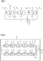
- the Fig. 1 shows a schematic representation of a first embodiment of an apparatus for generating random bits.
- the device 1 is constructed in the manner of an n-channel or n-track ring oscillator.
- combinatorial digital circuits 2 1 to 2 m are serially connected in series.
- the combinatorial digital circuits 2 1 to 2 m can also be understood as logic gates or imaging devices for a respective combinatorial mapping.
- the inputs and outputs are not explicitly indicated.
- a respective imaging device 2 i receives insofar E i1 to E in input signals and outputs A i1 to A ip output signals.
- the connection between input and output signals is over realized a combinational mapping K i .
- n p
- the K 1 to K m combinatorial images are concatenated successively and the imaging result or the output signals A m1 to A mp are performed as input signals E 11 to E 1n to the first imaging device 2 1 .
- a feedback results as in a ring oscillator.
- imaging devices 2 1 - 2 m form an annular topology
- a forward coupling of output signals A m1 to A mn at inputs downstream linkage imaging devices 2 1 - 2 m can cause jittery signal edges propagate through the concatenated imaging devices 2 1 - 2 m while jittering is amplified and multiplied.
- the respective imaging device 2 i with the implemented combinatorial mapping K i can also be referred to as a node, gate or combinatorial digital circuit.
- the imaging devices in the 2 1 to 2 m implemented combinatorial images K 1 to K m are chosen so that a change of a respective input bit or a logical state of an input signal E ij on average leads to changes in more than one of the output bits of the respective node or the respective imaging device.
- jitter that is present in the signals E 11 to E mn or A 11 to A mn accumulates and multiplies when passing through the linked imaging devices 2 1 to 2 m .
- the respective signal transit time in an imaging device or a logic or combinatorial gate 2 i is essentially the same for all input signals E i1 to E in , so that, due to the implemented combinatorial mapping K i, the change of a logic state at an input signal E ij substantially simultaneously to logic changes to one or more output signals A il with l ⁇ ⁇ 1, 2, ... n ⁇ . As such, there are n channels with random waveforms caused by the jitter caused by the switching elements constituting the digital imaging devices.
- a scanning device 4 which detects, for example, one or more of the output signals A m1 to A mn of the imaging device 2 m and, since a random signal waveform results, from which a random bit signal ZB is derived. For example, it is possible to clock or, if required, to pick up and record a signal level and to interpret it as an H or L or 1- or 0-bit value.
- the device or the random bit generator 1 it is possible to put the device or the random bit generator 1 in an initial state in which there is no fixed point. This takes place, for example, by virtue of the fact that, for example, the input signals E 11 to E 1n for the first imaging device 2 1 are given well-defined levels over the entire bit width n.
- the feedback line between the imaging device 2 m and the imaging device 2 1 may be temporarily interrupted. Then let the oscillation run free, so that random signal forms result in the n tapped channels or paths.
- Fig. 1 is optionally indicated that also another feedback path 3 (shown in phantom) can be implemented.
- another feedback path 3 shown in phantom
- the schematically indicated device for generating random bits 1 can be realized, in particular, at low cost in FPGA or ASIC devices. Compared to classical single-channel ring oscillators, random bits can be generated with a higher data rate since, in particular, the randomly favorable jitter is potentially multiplied n times with the aid of the multiple channels. It is unlikely that Jitter's contributions compensate each other because of the many channels and images. In this respect, a random number generator with a high random bit generation frequency can be realized in a cost-effective manner.
- Fig. 2 is a further embodiment of an apparatus for generating random bits indicated.
- the random bit generator 10 is implemented by means of an FPGA chip.
- m 10 combinatorial gates or imaging devices 2 1 to 2 10 connected in series and fed back.
- the combinational gates 2 1 to 2 10 each have four inputs and four outputs, resulting in a four-channel or four-track ring oscillator.
- the combinatorial images, which are realized by the gates 2 1 to 2 10 result from lookup tables 5 1 to 5 10 .
- the input signals E q1 - E q4 and the output signals A q1 - A q4 represent logical states 0 or 1 and L or H, respectively, although due to the "randomness" and heavy application of random jitter there are rather no well defined logic levels in the hardware-implemented circuitry for generating random bits.
- the table can be implemented as a look-up table for forming the mapping device 2q.
- a bijective mapping is implemented so that each possible bit pattern of four input bits or input signal states E q1 , E q2 , E q3 , E q4 occurs exactly once at the outputs of the mapping device 2q as output signal states A q1 , A q2 , A q3 , A q4 .
- An input bit pattern of 0010 results in an output bit pattern 0011 (see third row of the table).
- the signal edges which correspond to the state changes, applied to other jitters and "copied" to several, in the present example to 2.75 output signals.
- a jittery input signal is converted or imaged into a plurality of jittery output signals, additional jitter being supplemented by the respective mapping itself.
- the jitter which is used as a random phenomenon, is thus amplified and distributed over several channels.
- the combinatorial mapping K q represented as an example in tabular form, can be represented equivalently in the form of Boolean functions.
- OR is a logical OR
- AND is a logical AND
- NOT is a logical NOT.
- the combinatorial mappings may be used as a logical gate mappings in place of a lookup table above illustration are realized.
- a q 3 EMERGENCY XOR e q 1 . e q 2 . e q 4 . AND e q 4 e q 2 e q 1 .
- the output signal A q4 is independent of a state change of the input signal E q2 .
- An even more optimized construction of the combinatorial maps K q provides that a respective output signal depends on as many input signals as possible. It would be particularly preferable for each output signal of a combinatorial mapping to be dependent on all input signals for the mapping. Then jitter in the signals would multiply and amplify very well.
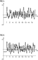
- Fig. 3 to 6 show variants of random bit signals ZB used with an FPGA implementation of the in Fig. 2 are generated circuit shown.
- the y-axis shows the signal level in volts and the x-axis the time in nanoseconds. Random bijective n-to-n bitmaps were used. It can be seen that with the same starting values, even after a short time, for example after 10 ns, completely different signal forms occur, which are random. In this respect, the random waveforms can be used as a basis for determining random bit values.
- the Fig. 7 shows a schematic representation of a third embodiment of an apparatus for generating random bits.
- the device 100 implements several optional modifications of the related art Fig. 1 and 2 Devices 1 and 10 explained.
- the device 100 comprises five imaging devices 2 1 - 2 5 , each implementing a combinatorial mapping K 1 - K 5 .
- the images K 1 and K 5 each represent four input signals to four output signals.
- the imaging devices 2 1 and 2 5 inputs for four input signals E 11 - E 14 and E 51 - E 54 and the same number of outputs for each four output signals A 11 - A 14 and A 51 - A 54th
- the figures K 2 and K 3 form three input signals E 21 , E 22 , E 23 and E 31 , E 32 , E 33 to four output signals A 21 - A 24 and A 31 - A 34 from.
- the map K 4 is a four-by-three map and generates three output signals A 41 , A 42 , A 43 from four input signals E 41 -E 44 .
- the output signal A 23 is fed forward or fed back as input signal E 51 depending on the perspective.
- the output signals A 13 and A 14 are logically rounded by means of an AND gate 11 and supplied as input signal E 23 of the imaging device 2 2 .
- the output signals A 52 and A 53 are logically ORed by means of an OR gate 11, inverted with an inverter 8, and input signal E 11 of the imaging device 2 1 supplied.
- the output signal A 31 is inverted by means of an inverter 6 to the input signal E 44 .
- the maps K 1 - K 5 are arranged so that a change in state of an input signal is mapped on average to more than one output signal.
- a bijective image as explained with respect to the table above can be used.
- a feedback loop results, for example, from the signals A 14 , E 23 , A 23 , E 51 and A 51 , due to the design of the maps K 1 , K 2 and K 5 signal edges are also transferred to other paths in the device 100 and cause random waveforms.
- the signals A 33 and A 54 are each tapped with the aid of toggle flip-flops 9.
- the respective T flip-flop 9 serves as a counter which counts rising signal edges as 0 ⁇ 1 passes modulo 2.
- a respective random bit can be tapped.
- the proposed device and the underlying method are particularly suitable for implementation in ASICs.
- the logical functions of the imaging devices preferably have the same logical depth to achieve the same signal propagation time of the combinatorial mappings.
- lookup tables can also be dispensed with.
- the invention thus enables rapid random bit generation with low hardware expenditure.
Description
Die vorliegende Erfindung betrifft eine Vorrichtung und ein Verfahren zum Erzeugen eines oder mehrerer Zufallsbits. Es wird zum Beispiel eine Zufallsbitfolge erzeugt, welche als binäre Zufallszahl verwendet wird. Die vorgeschlagenen Vorrichtungen und Verfahren zum Erzeugen von Zufallsbits dienen beispielsweise der Implementierung von Zufallszahlengeneratoren.The present invention relates to an apparatus and method for generating one or more random bits. For example, a random bit sequence is generated which is used as a binary random number. The proposed devices and methods for generating random bits serve, for example, the implementation of random number generators.
In sicherheitsrelevanten Anwendungen, beispielsweise bei asymmetrischen Authentifikationsverfahren, sind Zufallsbitfolgen als binäre Zufallszahlen notwendig. Dabei ist es gewünscht, insbesondere bei mobilen Anwendungen einen möglichst geringen Hardwareaufwand zu betreiben. Bekannte Maßnahmen, um Zufallszahlen zu erzeugen, sind beispielsweise Pseudozufallszahlen, analoge Zufallsquellen, Ringoszillatoren und deren Abwandlungen.In security-relevant applications, for example in asymmetric authentication methods, random bit sequences are necessary as binary random numbers. It is desired, in particular for mobile applications to operate as little hardware as possible. Known measures for generating random numbers are, for example, pseudo-random numbers, analogue random sources, ring oscillators and their modifications.
Bei Pseudozufallszahlen werden Seeds verwendet, von denen ausgehend deterministische Pseudozufallszahlen berechnet werden. Zur Erzeugung des Seeds wird in der Regel ein physikalischer Zufallsgenerator verwendet. Als analoge Zufallsquellen werden Rauschquellen, wie z.B. das Rauschen von Zenerdioden, verstärkt und digitalisiert. Dabei ist die Verbindung von digitaler mit analoger Schaltungstechnik meist nur aufwändig zu verwirklichen.For pseudo-random numbers, seeds are used, from which deterministic pseudorandom numbers are calculated. To create the seed, a physical random number generator is usually used. As analog random sources, noise sources such as e.g. the noise of zener diodes, amplified and digitized. At the same time, the connection between digital and analog circuit technology is usually difficult to realize.
Bei Ringoszillatoren, die aus einer ungeraden Anzahl von hintereinander geschalteten Invertern aufgebaut sind, ergeben sich zufällige Jitter aus schwankenden Durchlaufzeiten der Signale durch die Inverter. Diese Jitter, also eine unregelmäßige zeitliche Schwankung in Zustandsänderungen der durch die Inverter geschickten Signale, können bei mehrfachen Durchläufen durch die Ringoszillatorschaltung akkumuliert werden, so dass letztlich ein zufälliges analoges Signal entsteht. Nachteilig bei Ringoszillatoren ist häufig die notwendige lange Zeit vom Start der Schwingung bis ein brauchbar zufälliges Signal aufgrund der Jitter-Akkumulierung entsteht. Daher ergeben sich meist niedrige nicht akzeptable Datenerzeugungsraten bei Ringoszillatoren. Ferner ist möglich, dass die sich addierenden Jitter-Beiträge sich auch selbst wieder aufheben, so dass im Mittel zufällige kurze Gatterlaufzeiten durch zufällige längere Gatterlaufzeiten kompensiert werden.For ring oscillators, which are made up of an odd number of inverters connected in series, random jitter results from fluctuating throughput times of the signals through the inverters. These jitter, that is, an irregular variation with time in state changes of the signals sent by the inverters, can be accumulated in multiple passes through the ring oscillator circuit, so that ultimately a random analog signal arises. A disadvantage of ring oscillators is often the necessary long time from the start of the oscillation until a usable random signal due to the jitter accumulation arises. Therefore, mostly low unacceptable data generation rates arise for ring oscillators. It is also possible that the adding jitter contributions also cancel themselves out, so that on average random short gate delays are compensated by random longer gate delays.
Fibonacci- und Galois-Ringoszillatoren erzeugen schneller zufällige Signalformen als klassische Ringoszillatoren. Allerdings werden verschiedene digitale Gatter wie XOR- und NOT-Gatter eingesetzt. Dadurch können sich insbesondere bei Implementierungen auf ASICs große Geschwindigkeitsunterschiede der Gattertypen ergeben. Häufig besteht der Wunsch, mit Hilfe von FPGAs (Field Programmable Gate Arrays) Zufallsbitfolgen zu erzeugen. Allerdings können auch bei diesen Digitalbausteinen beispielsweise aufgrund von Umgebungstemperaturschwankungen periodische Schwingungen einsetzen, die nur eine geringe Entropie oder Zufälligkeit in den Signalen haben.Fibonacci and Galois ring oscillators generate random waveforms faster than classical ring oscillators. However, various digital gates such as XOR and NOT gates are used. This can result in particular in implementations on ASICs large speed differences of the gate types. Often, there is a desire to generate random bit sequences using FPGAs (Field Programmable Gate Arrays). However, even with these digital components, for example due to ambient temperature fluctuations, periodic oscillations can occur which have only a low degree of entropy or randomness in the signals.
Die europäische Patentanmeldung
Daher besteht eine Aufgabe der vorliegenden Erfindung darin, eine verbesserte Vorrichtung und/oder ein Verfahren zum Erzeugen von Zufallsbits bereitzustellen.Therefore, it is an object of the present invention to provide an improved apparatus and / or method for generating random bits.
Demgemäß wird eine Vorrichtung zum Erzeugen von Zufallsbits vorgeschlagen, die umfasst: mehrere Abbildungseinrichtungen, wobei eine jeweilige Abbildungseinrichtung eingerichtet ist, eine vorgegebene Anzahl n Eingangssignale mit Hilfe einer kombinatorischen Abbildung in eine vorgegebene Anzahl p Ausgangssignale abzubilden. Dabei sind die Abbildungseinrichtungen miteinander verkettet, und es ist mindestens eine Rückkopplungsschleife ausgebildet. Die Rückkopplungsschleife ist insbesondere derart ausgebildet, dass eine Zustandsänderung mindestens eines Ausgangssignals einer ausgewählten Abbildungseinrichtung als eine Zustandsänderung mindestens eines Eingangssignals einer anderen Abbildungseinrichtung zugeführt ist.Accordingly, an apparatus for generating random bits is proposed which comprises: a plurality of imaging devices, wherein a respective imaging device is set up to image a predetermined number n of input signals into a predefined number p of output signals by means of a combinatorial mapping. Here are the imaging devices concatenated with each other, and at least one feedback loop is formed. The feedback loop is in particular designed such that a change in state of at least one output signal of a selected imaging device as a change in state at least an input signal is fed to another imaging device.
Vorzugsweise ist die andere Abbildungseinrichtung keine direkt benachbarte Abbildungseinrichtung.Preferably, the other imaging device is not a directly adjacent imaging device.
Dabei liegt insbesondere eine Rückkopplungsschleife derart vor, dass eine Zustandsänderung mindestens eines Rückkopplungsausgangssignals einer bestimmten Abbildungseinrichtung als eine Zustandsänderung mindestens eines Eingangssignals einer anderen Abbildungseinrichtung derart zugeführt ist, dass eines oder mehrere Ausgangssignale der bestimmten Abbildungseinrichtung von der Zustandsänderung des Rückkopplungsausgangssignals beeinflusst wird.In particular, a feedback loop is provided in such a way that a state change of at least one feedback output signal of a specific imaging device is supplied as a change in state of at least one input signal of another imaging device such that one or more output signals of the particular imaging device is influenced by the state change of the feedback output signal.
Ferner ist mindestens eine kombinatorische Abbildung derart eingerichtet, dass eine Zustandsänderung eines Eingangssignals einer jeweiligen Abbildungseinrichtung im Mittel auf mehr als ein Ausgangssignal der jeweiligen Abbildungseinrichtung abgebildet wird.Furthermore, at least one combinatorial mapping is set up in such a way that a state change of an input signal of a respective imaging device is mapped on average to more than one output signal of the respective imaging device.
Die Anzahl der n Eingangssignale einer jeweiligen Abbildungseinrichtung kann der Anzahl p der Ausgangssignale entsprechen. Es ist aber auch denkbar, dass n ungleich p ist, also dass mit Hilfe einer jeweiligen Abbildungseinrichtung die Zustände der Eingangssignale auf Zustände von Ausgangssignalen abgebildet werden, wobei die Anzahl der Ausgangssignale kleiner oder größer als die Anzahl der Eingangssignale für eine jeweilige Abbildungseinrichtung ist.The number of n input signals of a respective imaging device may correspond to the number p of the output signals. However, it is also conceivable that n is not equal to p, ie that with the aid of a respective imaging device, the states of the input signals are mapped to states of output signals, wherein the number of output signals is smaller or larger than the number of input signals for a respective imaging device.
Die Abbildungseinrichtungen können logische oder kombinatorische Gatter sein, die insbesondere eine bijektive Abbildung von n Eingangssignalen auf n Ausgangssignale realisiert. Die Eingangssignale schwanken zwischen Pegeln, die logischen Zuständen, wie Bits 1 bzw. High oder 0 bzw. Low zugeordnet werden können. Unter einer bijektiven Abbildung versteht man eine eineindeutige Abbildung zwischen den 2n möglichen logischen Werten der Eingangssignale und den 2n logischen Werten der Ausgangssignale.The imaging devices may be logic or combinatorial gates, which in particular realize a bijective mapping of n input signals to n output signals. The input signals fluctuate between levels that can be assigned to logic states such as bits 1 or high or 0 or low. A bijective mapping is a one-to-one mapping between the 2 n possible logical values of the input signals and the 2 n logic values of the output signals.
Insofern ergibt sich mit Hilfe der Abbildungseinrichtungen in Ausführungsformen der Vorrichtung ein n-Spur-Ringoszillator. Die Abbildungseinrichtungen können auch als Knoten oder Gatter bezeichnet sein. Die jeweilige kombinatorische Abbildung ist insbesondere derart eingerichtet, dass im Mittel bei einer Zustandsänderung eines Eingangssignals an mehr als einem Ausgangssignal ein Zustandswechsel erfolgt. Das führt dazu, dass ein jeweiliger Jitter des Eingangssignals auf mehrere Ausgangssignale abgebildet wird und daher verstärkt wird. Ein einmal aufgetretener Jitter in einem Signal wird mit Hilfe der Abbildungseinrichtungen bzw. der darin implementierten kombinatorischen Abbildungen auf mehrere Ausgangsspuren kopiert, so dass sich Jitter-Komponenten kaum kompensieren können.In this respect, an n-track ring oscillator results with the aid of the imaging devices in embodiments of the device. The imaging devices may also be referred to as nodes or gates. The respective combinatorial mapping is set up in particular in such a way that, on average, a state change ensues on a change of state of an input signal at more than one output signal. As a result, a respective jitter of the input signal is mapped to a plurality of output signals and therefore amplified. Once a jitter has occurred in a signal, it is copied to a plurality of output tracks with the aid of the imaging devices or the combinatorial mappings implemented therein, so that jitter components can hardly be compensated.
Man kann bei der Vorrichtung auch von einer Mehrspur-Ringoszillatorschaltung sprechen. Gegenüber klassischen einspurigen Ringoszillatoren besteht insbesondere der Vorteil, dass mit einer höheren Datenrate zufällige Bitwerte abgegriffen werden können. Beispielsweise kann ein Zufallsbitsignal an einem oder mehreren der Datenpfade, welche sich durch die n Ein- bzw. Ausgangssignale ergeben, abgeleitet werden.One can also speak of a multi-track ring oscillator circuit in the device. In contrast to classical single-track ring oscillators, there is the particular advantage that random bit values can be tapped with a higher data rate. For example, a random bit signal may be derived on one or more of the data paths resulting from the n input and output signals.
Man kann sagen, die Vorrichtung entwickelt "Schwingungen" oder Signalwechsel propagieren im Kreis. Vorzugsweise hängt mindestens eines der Ausgangssignale kausal von sich selbst ab, indem es rückgekoppelt wird, wobei die Rückkopplung mit Hilfe mehrerer zwischengeschalteter Abbildungen erfolgt.It can be said that the device develops "oscillations" or signal changes propagate in a circle. Preferably, at least one of the outputs causally depends on itself by being fed back, the feedback being done by means of a plurality of interleaved mappings.
In Ausführungsformen der Vorrichtung ist mindestens eine kombinatorische Abbildung derart eingerichtet, dass die Eingangssignale unter Beaufschlagung eines Jitters und einer logischen Funktion auf die Ausgangssignale abgebildet werden. Durch die hardwaremäßige Implementierung der kombinatorischen Abbildung durch die Abbildungseinrichtungen können sich Jitter, also Schwankungen, in dem zeitlichen Verlauf von Signalflanken ergeben. Dieser Jitter wird dann durch Vollziehen der logischen Funktion, also der Abbildung der Kombination von n Eingangssignalen oder Bitwerten auf n Ausgangssignale oder Bitwerte jeweils weitergeführt und akkumuliert sich über die Durchläufe und Rückkopplung der Abbildungseinrichtungen.In embodiments of the device, at least one combinatorial mapping is arranged such that the input signals are mapped to the output signals while applying a jitter and a logical function. Due to the hardware implementation of the combinatorial mapping by the imaging devices, jitter, ie fluctuations, can result in the time course of signal edges. This jitter is then completed the logical function, ie the mapping of the combination of n input signals or bit values to n output signals or bit values is continued in each case and accumulates over the passes and feedback of the imaging devices.
Vorzugsweise sind zumindest einige der Abbildungen keine kombinatorischen Abbildungen, welche ausschließlich eine Permutation der Eingangssignale auf die Ausgangssignale liefern. Eine Permutation der Eingangssignale liegt insbesondere dann vor, wenn die Ausgangssignale den Eingangssignalen entsprechen, oder lediglich durch eine Änderung der Reihenfolge aus den Eingangssignalen entstehen. Bei einer Permutation ergibt sich keine "Vervielfältigung" des Jitters.Preferably, at least some of the mappings are not combinatorial mappings which exclusively provide a permutation of the input signals to the output signals. A permutation of the input signals is present in particular when the output signals correspond to the input signals, or arise only by a change in the order of the input signals. In a permutation there is no "duplication" of the jitter.
In Ausführungsformen der Vorrichtung zum Erzeugen von Zufallsbits sind die Abbildungseinrichtungen derart eingerichtet, dass deren Signaldurchlaufzeiten gleich sind. Durch möglichst gleiche Signallaufzeiten wird das Risiko vermindert, dass sich Jitter-Beiträge gegenseitig kompensieren können. Außerdem wird eine Implementierung in der Art von ASICs oder FPGAs erleichtert. Beispielsweise sind die Abbildungseinrichtungen so eingerichtet, dass alle mögliche Zustandswechsel an den jeweiligen Ausgängen alle innerhalb eines Toleranzintervalls von 100 ps und bevorzugt innerhalb von 50 ps erfolgen.In embodiments of the device for generating random bits, the imaging devices are arranged such that their signal transit times are the same. The same signal propagation times reduce the risk that jitter contributions can compensate each other. It also facilitates implementation in the manner of ASICs or FPGAs. For example, the mapping means are arranged so that all possible state changes at the respective outputs are all within a tolerance interval of 100 ps and preferably within 50 ps.
In Ausführungsformen der Vorrichtung umfasst mindestens eine Abbildungseinrichtung einer Lookup-Table bzw. eine Nachschlagetabelle zur Implementierung der kombinatorischen Abbildung. Es ist auch möglich, dass alle Abbildungseinrichtungen mit einer jeweiligen Lookup-Table versehen sind. Lookup-Tables können einfach ausgelesen werden und erfordern nur einen geringen Hardwareaufwand. Häufig sind in programmierbaren Logikchips, wie FPGAs, entsprechende Felder oder bereits Tabellen vorgesehen.In embodiments of the device, at least one mapping device comprises a lookup table for implementing the combinatorial mapping. It is also possible that all imaging devices are provided with a respective lookup table. Lookup tables can be easily read and require only a small amount of hardware. Frequently in programmable logic chips, such as FPGAs, corresponding fields or already tables are provided.
In Ausführungsformen der Vorrichtung können die Lookup-Tables mit zufälligen Bitwerten unter Verwendung von Zufallselementen gefüllt werden. Es ist beispielsweise möglich, die Lookup-Tables, die in Abhängigkeit von einem Eingangsbitmuster an Eingängen der Abbildungseinrichtungen ein entsprechendes Ausgangsbitmuster an Ausgängen liefern, so zu erzeugen, dass die durch die Lookup-Table repräsentierte Abbildung zufällig aus allen (2n) ! Bijektionen von n logischen Signalen auf n logische Signale ausgewählt wird. Vorzugsweise sind in den Abbildungseinrichtungen jeweils unterschiedliche kombinatorische Abbildungen implementiert.In embodiments of the device, the lookup tables may be random bit values using random elements be filled. For example, it is possible to generate the lookup tables that provide a corresponding output bit pattern at outputs in response to an input bit pattern at inputs of the mapping devices such that the representation represented by the lookup table happens to be from all (2 n )! Bijections of n logical signals to n logical signals is selected. Preferably, different combinatorial mappings are implemented in the imaging devices.
In Ausführungsformen der Vorrichtung bilden die miteinander verketteten Abbildungseinrichtungen eine mehrspurige Ringoszillatorschaltung aus.In embodiments of the device, the concatenated imaging devices form a multi-track ring oscillator circuit.
Es ist denkbar, dass in der Vorrichtung mehrere Rückkopplungszweige von verketteten Abbildungseinrichtungen vorliegen. Es ist beispielsweise möglich, mehrere Einzelketten zu verschiedenen Rückkopplungen zusammenzuschalten.It is conceivable that there are a plurality of feedback branches of linked imaging devices in the device. For example, it is possible to interconnect multiple single chains into different feedbacks.
In Ausführungsformen der Vorrichtung ist die Vorrichtung derart eingerichtet, dass insbesondere bei einem erstmaligen Einkoppeln von Eingangssignalen die Eingangssignale derart vorgegeben sind, dass die Vorrichtung nicht in einem Fixpunkt vorliegt. Beispielsweise können feste wohldefinierte Pegel an die Eingänge einer der Abbildungseinrichtungen angelegt werden, um aus einem wohldefinierten Zustand zu starten. Anschließend ergibt sich durch die Rückkopplung und die verkettete Anwendung der kombinatorischen Abbildungen auf die Signale ein n oder p Bit breites Zufallsbitsignal.In embodiments of the device, the device is set up in such a way that the input signals are predetermined in such a way that the device is not present in a fixed point, in particular when the input signals are coupled in for the first time. For example, fixed well-defined levels may be applied to the inputs of one of the imaging devices to start from a well-defined state. Subsequently, the feedback and the concatenated application of the combinatorial mappings to the signals results in an n or p bit wide random bit signal.
Die Vorrichtung ist vorzugsweise insbesondere derart eingerichtet, dass sie keinen Fixpunkt aufweist. Dazu werden die kombinatorischen Abbildungen derart ausgewählt und implementiert, dass kein Fixpunkt vorliegt.The device is preferably arranged in particular such that it has no fixed point. For this purpose, the combinatorial mappings are selected and implemented in such a way that there is no fixed point.
Vorzugsweise ist die vorgegebene Anzahl n beziehungsweise p von Eingangs- beziehungsweise Ausgangssignalen mindestens drei. In Ausführungsformen ist die Bitbreite oder die Anzahl n beziehungsweise p von vorgegebenen Eingangs- beziehungsweise Ausgangssignalen an den Abbildungseinrichtungen vier oder mehr.Preferably, the predetermined number n or p of input or output signals is at least three. In embodiments, the bit width or the number n or p of predetermined input or Output signals at the imaging devices four or more.
In Ausführungsformen der Vorrichtung ist eine Abtastvorrichtung zum Abtasten eines oder mehrerer Ausgangssignale an Ausgängen einer Abbildungseinrichtung vorgesehen. Die Abtastvorrichtung kann auch ein jeweiliges Ein- oder Ausgangssignal an unterschiedlichen Abbildungseinrichtungen erfassen. Das Abtasten erfolgt beispielsweise getaktet oder zu vorgegebenen anderen Zeitpunkten und dient der Ableitung eines Bitwertes H oder L, der aufgrund des stark schwankenden zufälligen Signals eine hohen Entropie bzw. Zufälligkeit aufweist.In embodiments of the apparatus, a scanning device is provided for scanning one or more output signals at outputs of an imaging device. The scanning device can also detect a respective input or output signal at different imaging devices. The sampling takes place, for example, clocked or at predetermined other times and serves to derive a bit value H or L, which has a high entropy or randomness due to the strongly fluctuating random signal.
In Ausführungsformen umfasst die Abtastvorrichtung mindestens ein Zwischenspeicherelement. Das Zwischenspeicherelement kann ein Flip-Flop, wie zum Beispiel ein T-Flip-Flop oder eine Latch-Einrichtung aufweisen. Denkbar sind auch einer oder mehrere Zähler zum Erfassen von Signalflanken oder Zustandswechseln einzelner Signale. Ein T-Flip-Flop ist insbesondere geeignet, steigende oder fallende Signalflanken modulo 2 zu zählen.In embodiments, the scanning device comprises at least one buffer element. The latching element may comprise a flip-flop, such as a T-flip-flop or a latch device. Also conceivable are one or more counters for detecting signal edges or state changes of individual signals. A T-flip-flop is particularly suitable for counting rising or falling signal edges modulo 2.
Die Erfassungseinrichtung kann derart eingerichtet sein, dass ein Ausgangssignal in Abhängigkeit von einem anderen Ausgangssignal abgetastet wird. Denkbar ist zum Beispiel, dass eine Signalflanke eines ersten Ausgangssignals das Abtasten eines anderen Ausgangssignals triggert oder hervorruft.The detection device may be configured such that an output signal is sampled in dependence on another output signal. It is conceivable, for example, that a signal edge of a first output signal triggers or causes the sampling of another output signal.
In Ausführungsformen ist die Vorrichtung Teil einer FPGA-Einrichtung oder einer ASIC-Einrichtung.In embodiments, the device is part of an FPGA device or an ASIC device.
Es wird darüber hinaus ein Verfahren zum Erzeugen von Zufallsbits vorgeschlagen, bei dem mehrere kombinatorische Abbildungen verkettet nacheinander durchgeführt werden. Dabei bildet eine jeweilige kombinatorische Abbildung eine vorgegebene Anzahl n Eingangssignale auf eine vorgegebene Anzahl p Ausgangssignale ab. Durch die Verkettung der kombinatorischen Abbildungen wird mindestens eine Rückkopplungsschleife gebildet. Dabei wird mindestens eine kombinatorische Abbildung derart gewählt, dass eine Zustandsänderung eines Eingangssignals durch die kombinatorischen Abbildungen im Mittel auf mehr als ein Ausgangssignal abgebildet wird. Ein jeweiliges Eingangssignal kann z.B. einen Bitwert darstellen.In addition, a method for generating random bits is proposed, in which a plurality of combinatorial pictures are performed concatenated one after the other. In this case, a respective combinational image maps a predetermined number n of input signals to a predetermined number p of output signals. By linking the combinatorial mappings, at least one feedback loop is formed. In doing so, at least one combinatorial image is created chosen such that a change in state of an input signal is mapped by the combinatorial mappings on average to more than one output signal. A respective input signal may represent a bit value, for example.
Vorzugsweise wird die mindestens eine Rückkopplung derart gebildet, dass eine Zustandsänderung mindestens eines Ausgangssignals einer ausgewählten kombinatorischen Abbildung als eine Zustandsänderung mindestens eines Eingangssignals einer anderen kombinatorischen Abbildung zugeführt wird.Preferably, the at least one feedback is formed in such a way that a change in state of at least one output signal of a selected combinational mapping as a change in state of at least one input signal is fed to another combinatorial mapping.
Die kombinatorischen Abbildungen können als n auf p Abbildungen bezeichnet werden.The combinatorial mappings can be referred to as n on p mappings.
Das Verfahren kann insbesondere über geeignete Beschreibungssprachen, beispielsweise VHDL oder Verilog, auf oder in einer FPGA- oder ASIC-Vorrichtung implementiert werden. Bei der FPGA-Vorrichtung bzw. dem Verfahren sind die Abbildungseinrichtungen vorzugsweise derart eingerichtet, dass Zustandsänderungen an einem Eingangssignal der n Eingangssignale in Abhängigkeit von der kombinatorischen Abbildung zu einem gleichen Zeitpunkt einen Zustandswechsel in einem oder mehreren der p Ausgangssignale möglichst zeitgleich hervorrufen.The method can in particular be implemented on or in an FPGA or ASIC device via suitable description languages, for example VHDL or Verilog. In the case of the FPGA device or the method, the imaging devices are preferably set up in such a way that state changes on an input signal of the n input signals as a function of the combinatorial mapping cause a state change in one or more of the p output signals at the same time.
Weitere mögliche Implementierungen der Erfindung umfassen auch nicht explizit genannte Kombinationen von zuvor oder im Folgenden bezüglich der Ausführungsbeispiele beschriebenen Vorrichtungen oder Verfahrensvarianten. Dabei wird der Fachmann auch Einzelaspekte als Verbesserungen oder Ergänzungen zu der jeweiligen Grundform der Erfindung hinzufügen oder abändern.Further possible implementations of the invention also include not explicitly mentioned combinations of devices or method variants described above or below with regard to the exemplary embodiments. The skilled person will also add or modify individual aspects as improvements or additions to the respective basic form of the invention.
Die oben beschriebenen Eigenschaften, Merkmale und Vorteile dieser Erfindung sowie die Art und Weise, wie diese erreicht werden, werden klarer und deutlicher verständlich im Zusammenhang mit der folgenden Beschreibung der Ausführungsbeispiele, die im Zusammenhang mit den Zeichnungen näher erläutert werden.The above-described characteristics, features, and advantages of this invention, as well as the manner in which they will be achieved, will become clearer and more clearly understood in connection with the following description of the embodiments, which will be described in detail in conjunction with the drawings.
Dabei zeigen:
- Fig. 1
- eine schematische Darstellung eines ersten Ausführungsbeispiels für eine Vorrichtung zum Erzeugen von Zufallsbits;
- Fig. 2
- eine schematische Darstellung eines zweiten Ausführungsbeispiels für eine Vorrichtung zum Erzeugen von Zufallsbits;
- Fig. 3 - 6
- zeitliche Verläufe von Zufallsbitsignalen, welche gemäß Ausführungsbeispielen des Verfahrens und der Vorrichtung zum Erzeugen von Zufallsbits erzeugt sind; und
- Fig. 7
- eine schematische Darstellung eines dritten Ausführungsbeispiels für eine Vorrichtung zum Erzeugen von Zufallsbits.
- Fig. 1
- a schematic representation of a first embodiment of an apparatus for generating random bits;
- Fig. 2
- a schematic representation of a second embodiment of an apparatus for generating random bits;
- Fig. 3 - 6
- time histories of random bit signals generated in accordance with embodiments of the method and apparatus for generating random bits; and
- Fig. 7
- a schematic representation of a third embodiment of an apparatus for generating random bits.
In den Figuren sind funktionsgleiche Elemente mit denselben Bezugszeichen versehen, sofern nichts anderes angegeben ist.In the figures, functionally identical elements are provided with the same reference numerals, unless stated otherwise.
Die
Jede Abbildungseinrichtung 2i hat n Eingänge für ein n Bit breites Eingangssignal Eij mit j = 1...n und p Ausgänge für ein p Bit-breites Ausgangssignal Aij mit j = 1...p. In der
Um eine Rückkopplung zu erzielen sind nicht notwendigerweise alle Ausgangssignale Am1 bis Amp als Eingangssignale E11 bis E1n einer signalpfadaufwärts verketteten Abbildungseinrichtung 21 zuzuführen. Prinzipiell genügt es, ein einzelnes Ausgangssignal Aij auszuwählen und einer im Signalweg oder Signalpfad vorgeschalten Abbildungseinrichtung 2k zuzuführen, sofern ein Zustandswechsel des an dem jeweiligen Eingang vorliegenden Signals Ekl ∼ Aij im Mittel zu Zustandswechseln in mehr als einem der Ausgangssignale Ako (o=1...n) führt. Je mehr Ausgangssignale rückgekoppelt werden, desto stärker wird ein vorliegender Jitter mit Hilfe der implementierten kombinatorischen Abbildungen K1 - Km verstärkt und auf die n "Kanäle" kopiert. Die Abbildungseinrichtungen müssen auch nicht zwingend dieselbe Anzahl von Ein- und Ausgängen n haben, der Einfachheit halber werden jedoch hier zunächst Beispiele mit der gleichen Anzahl von Eingangssignalen und Ausgangssignalen erläutert.In order to achieve a feedback, it is not necessary to feed all the output signals A m1 to A mp as input signals E 11 to E 1n to an image-path-uplinked imaging device 2 1 . In principle, it suffices to select a single output signal A ij and supply it to an imaging device 2 k connected upstream in the signal path or signal path, provided that a change in state of the signal E kl ~ A ij present at the respective input on average causes state changes in more than one of the output signals A ko ( o = 1 ... n). The more output signals are fed back, the stronger is an existing jitter with the help of the implemented combinatorial maps K 1 - K m amplified and copied to the n "channels". The imaging devices also need not necessarily have the same number of inputs and outputs n, but for the sake of simplicity, examples with the same number of input signals and output signals will first be explained here.
Da die Abbildungseinrichtungen 21 - 2m eine ringförmige Topologie ausbilden, kann auch eine Vorwärtskopplung von Ausgangssignalen Am1 bis Amn an Eingänge signalstromabwärts verketteter Abbildungseinrichtungen 21 - 2m dazu führen, dass jitterbehaftete Signalflanken durch die verketteten Abbildungseinrichtungen 21 - 2m propagieren und dabei Jitter verstärkt und vervielfältigt werden.Since the imaging devices 2 1 - 2 m form an annular topology, also a forward coupling of output signals A m1 to A mn at inputs downstream linkage imaging devices 2 1 - 2 m can cause jittery signal edges propagate through the concatenated imaging devices 2 1 - 2 m while jittering is amplified and multiplied.
Die jeweilige Abbildungseinrichtung 2i mit der implementierten kombinatorischen Abbildung Ki kann auch als Knoten, Gatter oder kombinatorische Digitalschaltung bezeichnet werden. Die in den Abbildungseinrichtungen 21 bis 2m implementierten kombinatorischen Abbildungen K1 bis Km sind so gewählt, dass eine Veränderung eines jeweiligen Input-Bits bzw. eines logischen Zustandes eines Eingangssignals Eij im Mittel zu Änderungen in mehr als einem der Output-Bits des jeweiligen Knotens bzw. der jeweiligen Abbildungseinrichtung führt. Insofern akkumulieren und vervielfältigen sich Jitter, die in den Signalen E11 bis Emn bzw. A11 bis Amn vorliegen, beim Durchlauf durch die verketteten Abbildungseinrichtungen 21 bis 2m.The respective imaging device 2 i with the implemented combinatorial mapping K i can also be referred to as a node, gate or combinatorial digital circuit. The imaging devices in the 2 1 to 2 m implemented combinatorial images K 1 to K m are chosen so that a change of a respective input bit or a logical state of an input signal E ij on average leads to changes in more than one of the output bits of the respective node or the respective imaging device. In this respect, jitter that is present in the signals E 11 to E mn or A 11 to A mn accumulates and multiplies when passing through the linked imaging devices 2 1 to 2 m .
Die jeweilige Signaldurchlaufzeit in einer Abbildungseinrichtung bzw. einem logischen oder kombinatorischen Gatter 2i ist für alle Eingangssignale Ei1 bis Ein im Wesentlichen gleich, so dass aufgrund der implementierten kombinatorischen Abbildung Ki der Wechsel eines logischen Zustands an einem Eingangssignal Eij im Wesentlichen zeitgleich zu logischen Wechseln an einem oder mehreren Ausgangssignalen Ail mit l ∈ {1, 2,...n} ist. Insofern ergeben sich n Kanäle mit zufälligen Signalformen, die von den Jittern hervorgerufen sind, die von den die digitalen Abbildungseinrichtungen aufbauenden Schaltelementen hervorgerufen sind.The respective signal transit time in an imaging device or a logic or combinatorial gate 2 i is essentially the same for all input signals E i1 to E in , so that, due to the implemented combinatorial mapping K i, the change of a logic state at an input signal E ij substantially simultaneously to logic changes to one or more output signals A il with l ∈ {1, 2, ... n}. As such, there are n channels with random waveforms caused by the jitter caused by the switching elements constituting the digital imaging devices.
Es ist eine Abtasteinrichtung 4 vorgesehen, die beispielsweise eines oder mehrere der Ausgangssignale Am1 bis Amn der Abbildungseinrichtung 2m erfasst und, da sich jeweils eine zufällige Signalverlaufsform ergibt, daraus ein Zufallsbitsignal ZB ableitet. Beispielsweise kann getaktet oder bei Bedarf ein Signalpegel abgegriffen und erfasst werden und dieser als ein H- oder L- bzw. 1- oder 0-Bitwert interpretiert werden.A
Es ist dabei möglich, die Vorrichtung bzw. den Zufallsbitgenerator 1 in einen Anfangszustand zu versetzen, bei dem kein Fixpunkt vorliegt. Dies erfolgt beispielsweise dadurch, dass über die gesamte Bitbreite n beispielsweise die Eingangssignale E11 bis E1n für die erste Abbildungseinrichtung 21 jeweils wohldefinierte Pegel erhalten. Darüber hinaus kann dann die Rückkopplungsleitung zwischen der Abbildungseinrichtung 2m und der Abbildungseinrichtung 21 vorübergehend unterbrochen sein. Anschließend lässt man die Oszillation frei laufen, so dass sich zufällige Signalformen in den n abgreifbaren Kanälen oder Pfaden ergeben.It is possible to put the device or the random bit generator 1 in an initial state in which there is no fixed point. This takes place, for example, by virtue of the fact that, for example, the input signals E 11 to E 1n for the first imaging device 2 1 are given well-defined levels over the entire bit width n. In addition, then the feedback line between the imaging device 2 m and the imaging device 2 1 may be temporarily interrupted. Then let the oscillation run free, so that random signal forms result in the n tapped channels or paths.
In der
Die schematisch angedeutete Vorrichtung zum Erzeugen von Zufallsbits 1 lässt sich insbesondere aufwandsgünstig in FPGA- oder ASIC-Einrichtungen realisieren. Gegenüber klassischen einkanaligen Ringoszillatoren lassen sich mit einer höheren Datenrate Zufallsbits erzeugen, da insbesondere der den Zufall begünstigende Jitter mit Hilfe der mehreren Kanäle potenziell n-fach vervielfältigt wird. Es ist durch die vielen Kanäle und Abbildungen unwahrscheinlich, dass Jitter-Beiträge einander kompensieren. Insofern kann aufwandsgünstig ein Zufallszahlengenerator mit einer hohen Zufallsbit-Erzeugungsfrequenz realisiert werden.The schematically indicated device for generating random bits 1 can be realized, in particular, at low cost in FPGA or ASIC devices. Compared to classical single-channel ring oscillators, random bits can be generated with a higher data rate since, in particular, the randomly favorable jitter is potentially multiplied n times with the aid of the multiple channels. It is unlikely that Jitter's contributions compensate each other because of the many channels and images. In this respect, a random number generator with a high random bit generation frequency can be realized in a cost-effective manner.
In der
In der folgenden Tabelle ist eine beispielhafte kombinatorische Abbildung Kq dargestellt, die n=4 Eingangszustände bzw. Eingangssignale Eq1 - Eq4 auf p=4 Ausgangszustände bzw. Ausgangssignale Aq1 - Aq4 abbildet. Zur Vereinfachung der Darstellung wird angenommen, dass die Eingangssignale Eq1 - Eq4 und die Ausgangssignale Aq1 - Aq4 logische Zustände 0 oder 1 bzw. L oder H repräsentieren, obwohl durch die "Verzufälligung" und starker Beaufschlagung mit zufälligen Jittern eher keine wohldefinierten logischen Pegel in der als Hardware bzw. als Schaltung implementierten Vorrichtung zum Erzeugen von Zufallsbits vorliegen.
Die Tabelle kann als Look-up-Tabelle zur Ausbildung der Abbildungseinrichtung 2q implementiert werden. Dabei wird eine bijektive Abbildung realisiert, sodass jedes mögliche Bitmuster aus vier Eingangsbits oder Eingangssignalzuständen Eq1, Eq2, Eq3, Eq4 genau einmal an den Ausgängen der Abbildungseinrichtung 2q als Ausgangssignalzustände Aq1, Aq2, Aq3, Aq4 auftritt.The table can be implemented as a look-up table for forming the mapping device 2q. In this case, a bijective mapping is implemented so that each possible bit pattern of four input bits or input signal states E q1 , E q2 , E q3 , E q4 occurs exactly once at the outputs of the mapping device 2q as output signal states A q1 , A q2 , A q3 , A q4 .
Für den Fall, dass die Eingangssignale Eq1, Eq2, Eq3, Eq4 initial ein Bitmuster 0000 bilden, was laut Zeile 1 der Tabelle auf Ausgangssignale 0100 abgebildet wird, und das Eingangssignal Eq1 einen Zustandswechsel vollzieht ergibt sich als Ausgangsbitmuster gemäß der zweiten Zeile der obigen Tabelle 1001. Das heißt, der Zustandswechsel des Eingangssignals Eq1 von 0 auf 1 wird mit Hilfe der kombinatorischen Abbildung Kq auf die drei Ausgangssignale Aq1, Aq3 und Aq4 "vervielfältigt". Denn das Ausgangssignal Aq1 ändert sich aufgrund der Zustandsänderung von Eq1 von 0 auf 1, das Ausgangssignal Aq3 von 1 auf 0 und das Ausgangssignal Aq4 von 0 auf 1.In the event that the input signals E q1 , E q2 , E q3 , E q4 initially form a bit pattern 0000, which is mapped to output signals 0100 according to line 1 of the table, and the input signal E q1 changes state, this results in That is, the state transition of the input signal E q1 from 0 to 1 is "multiplied" by means of the combinatorial mapping K q to the three output signals A q1 , A q3 and A q4 . Because the output signal A q1 changes from 0 to 1 due to the state change of E q1 , the output signal A q3 changes from 1 to 0 and the output signal A q4 changes from 0 to 1.
Ein Eingangsbitmuster von 0010 führt zu einem Ausgangsbitmuster 0011 (vgl. dritte Zeile der Tabelle). Ausgehend von einem Bitmuster 0000 und einem Zustandswechsel des Eingangssignals Eq2 von 0 auf 1 ergeben sich daher ebenfalls Zustandswechsel bei den drei Ausgangssignalen Aq1, Aq2 und Aq3, obgleich nur ein eingangsseitiger Zustandswechsel im Eingangssignal Eq2 erfolgt ist.An input bit pattern of 0010 results in an output bit pattern 0011 (see third row of the table). Starting from a bit pattern 0000 and a state change of the input signal E q2 from 0 to 1, therefore, there are also state changes in the three output signals A q1 , A q2 and A q3 , although only one input-side state change has occurred in the input signal E q2 .
Analog erkennt man für Eingangsbitmuster 0100 und 1000 ausgehend von 0000, dass sich drei oder alle vier Ausgangszustände ändern. Untersuchungen der Anmelderin für alle möglichen Zustandsänderungen von einzelnen Eingangssignalen ausgehend von allen 16 Eingangsbitmustern haben ergeben, dass bei der dargestellten Abbildung Kq im Mittel ein Zustandswechsel oder eine Zustandsänderung eines Eingangssignals Eqi zu 2,75 Zustandswechseln oder Zustandsänderungen in Ausgangssignalen führt.Similarly, for input bit patterns 0100 and 1000, starting from 0000, one can see that three or all four output states change. Investigations by the Applicant for all possible state changes of individual input signals on the basis of all 16 input bit patterns have shown that in the illustrated mapping K q a change of state or a state change of an input signal E qi results in 2.75 state changes or state changes in output signals.
Insofern werden bei der Umsetzung der kombinatorischen Abbildungen als elektronische Schaltkreise die Signalflanken, die den Zustandswechseln entsprechen, mit weiteren Jittern beaufschlagt und auf mehrere, im vorliegenden Beispiel auf 2,75 Ausgangssignale "kopiert". Insbesondere wird ein jitterbehaftetes Eingangssignal in mehrere jitterbehaftete Ausgangssignale überführt bzw. abgebildet, wobei durch die jeweilige Abbildung selbst zusätzliche Jitter ergänzt werden. Der Jitter, der als zufallsgebendes Phänomen genutzt wird, wird somit verstärkt und auf mehrere Kanäle verteilt.In this respect, in the implementation of combinatorial images as electronic circuits, the signal edges, which correspond to the state changes, applied to other jitters and "copied" to several, in the present example to 2.75 output signals. In particular, a jittery input signal is converted or imaged into a plurality of jittery output signals, additional jitter being supplemented by the respective mapping itself. The jitter, which is used as a random phenomenon, is thus amplified and distributed over several channels.
Die als Beispiel in Tabellenform wiedergegebene kombinatorischer Abbildung Kq kann äquivalent in Form von Booleschen Funktionen dargestellt werden.The combinatorial mapping K q , represented as an example in tabular form, can be represented equivalently in the form of Boolean functions.
Als disjunktive Normalform geschrieben lautet die kombinatorische Abbildung Kq: 


Dabei steht OR für eine logische ODER-Verknüpfung, AND für eine logische UND-Verknüpfung und NOT für eine logische NICHT-Verknüpfung. Zur hardwaremäßigen Implementierung können die kombinatorischen Abbildungen anstelle einer Look-up-Tabelle auch als Verknüpfung von logischen Gattern gemäß der obigen Darstellung realisiert werden. Die disjunktive Normalformdarstellung kann auch in eine algebraische Normalform umgeschrieben werden, welche ebenfalls zum Entwurf von entsprechenden logischen Schaltungen verwendet werden kann. Man kann schreiben: ![]()
![]()
![]()
![]()
![]()
![]()
![]()
![]()
Man erkennt in beiden Darstellungen, dass das Ausgangssignal Aq4 unabhängig von einem Zustandswechsel des Eingangssignals Eq2 ist. Eine noch weiter optimierte Konstruktion der kombinatorischen Abbildungen Kq sieht vor, dass ein jeweiliges Ausgangssignal von möglichst vielen Eingangssignalen abhängt. Besonders bevorzugt wäre, dass jedes Ausgangssignal einer kombinatorischen Abbildung von allen Eingangssignalen für die Abbildung abhängig ist. Dann würden sich Jitter in den Signalen besonders gut multiplizieren und verstärken.It can be seen in both representations that the output signal A q4 is independent of a state change of the input signal E q2 . An even more optimized construction of the combinatorial maps K q provides that a respective output signal depends on as many input signals as possible. It would be particularly preferable for each output signal of a combinatorial mapping to be dependent on all input signals for the mapping. Then jitter in the signals would multiply and amplify very well.
Die Signalpfade bzw. Kopplungen der kombinatorischen Gatter 21 bis 210 sind lediglich schematisch angedeutet. Nur zwischen den Gattern 25 und 26 sind explizit die vier Leitungen bzw. Verbindungen dargestellt.The signal paths or couplings of the combinational gates 2 1 to 2 10 are indicated only schematically. Only between the gates 2 5 and 2 6 , the four lines or connections are shown explicitly.
Man kann nun, nachdem der (n=4) Vier-Spur-Ringoszillator schwingt, beispielsweise das Signal A51, welches als Eingangssignal E61 an das kombinatorische Gatter 26 geführt ist, als zufällig schwankendes Signal betrachten. Eine Abtasteinrichtung 4 greift beispielsweise am Ausgang für das Signal A51 den schwankenden Pegel ab und erzeugt daraus ein Zufallsbit ZB.Now, after the (n = 4) four-track ring oscillator oscillates, for example, the signal A 51 , which is performed as input signal E 61 to the combinatorial gate 2 6 , consider as a randomly fluctuating signal. A
Untersuchungen der Anmelderin haben ergeben, dass günstige zufällige Signalkurven auch bei gleichen Anfangszuständen entstehen. Die
Auf der y-Achse ist der Signalpegel in Volt und auf der x-Achse die Zeit in Nanosekunden aufgetragen. Es wurden zufällige bijektive n-auf-n Bitabbildungen verwendet. Man erkennt, dass bei gleichen Startwerten bereits nach kurzer Zeit, beispielsweise nach 10 ns völlig unterschiedliche Signalformen entstehen, die zufällig verlaufen. Insofern können die zufälligen Signalformen als Basis zur Bestimmung von Zufallsbitwerten verwendet werden.The y-axis shows the signal level in volts and the x-axis the time in nanoseconds. Random bijective n-to-n bitmaps were used. It can be seen that with the same starting values, even after a short time, for example after 10 ns, completely different signal forms occur, which are random. In this respect, the random waveforms can be used as a basis for determining random bit values.
Die
Das Ausgangssignal A23 wird als Eingangssignal E51 je nach Betrachtungsweise vor- bzw. rückgekoppelt. Die Ausgangssignale A13 und A14 werden mit Hilfe eines UND-Gatters 11 logisch verundet und als Eingangssignal E23 der Abbildungseinrichtung 22 zugeführt. Ähnlich werden die Ausgangssignale A52 und A53 mit Hilfe eines ODER-Gatters 11 logisch verodert, mit einem Inverter 8 invertiert und als Eingangssignal E11 der Abbildungseinrichtung 21 zugeführt. Das Ausgangssignal A31 wird mit Hilfe eines Inverters 6 zum Eingangssignal E44 invertiert.The output signal A 23 is fed forward or fed back as input signal E 51 depending on the perspective. The output signals A 13 and A 14 are logically rounded by means of an AND
Es ergeben sich mehrere Rückkopplungen derart, dass eine Zustandsänderung mindestens eines Ausgangssignals einer Abbildungseinrichtung als eine Zustandsänderung mindestens eines Eingangssignals einer anderen Abbildungseinrichtung zugeführt ist. Außerdem sind die Abbildungen K1 - K5 so eingerichtet, dass eine Zustandsänderung eines Eingangssignals im Mittel auf mehr als ein Ausgangssignal abgebildet wird. Beispielsweise kann für die Abbildungseinrichtungen K1 und K5 eine bijektive Abbildung, wie es bezüglich der Tabelle oben erläutert wurde, verwendet werden.Several feedbacks result in such a way that a change in state of at least one output signal of an imaging device is supplied as a change in state of at least one input signal to another imaging device. In addition, the maps K 1 - K 5 are arranged so that a change in state of an input signal is mapped on average to more than one output signal. For example, for the imaging devices K 1 and K 5, a bijective image as explained with respect to the table above can be used.
Eine Rückkopplungsschleife ergibt sich zum Beispiel aus den Signalen A14, E23, A23, E51 und A51, wobei aufgrund der Ausgestaltung der Abbildungen K1, K2 und K5 Signalflanken auch auf weitere Pfade in der Vorrichtung 100 übertragen werden und zufällige Signalverläufe hervorrufen.A feedback loop results, for example, from the signals A 14 , E 23 , A 23 , E 51 and A 51 , due to the design of the maps K 1 , K 2 and K 5 signal edges are also transferred to other paths in the
Die Signale A33 und A54 werden jeweils mit Hilfe von Toggle-Flip-Flops 9 abgegriffen. Das jeweilige T-Flip-Flop 9 dient als Zähler, der steigende Signalflanken als 0→1 Durchgänge modulo 2 zählt. Am Datenausgang Q der Flip-Flops 9 ist dann ein jeweiliges Zufallsbit abgreifbar.The signals A 33 and A 54 are each tapped with the aid of toggle flip-
Die vorgeschlagene Vorrichtung und das zugrunde liegende Verfahren eignen sich insbesondere zur Implementierung in ASICs. Die logischen Funktionen der Abbildungseinrichtungen haben vorzugsweise dieselbe logische Tiefe, um eine gleiche Signallaufzeit der kombinatorischen Abbildungen zu erzielen. Auf Lookup-Tables kann insofern auch verzichtet werden. Die Erfindung ermöglicht also unter anderem eine schnelle Zufallsbiterzeugung bei geringem Hardwareaufwand.The proposed device and the underlying method are particularly suitable for implementation in ASICs. The logical functions of the imaging devices preferably have the same logical depth to achieve the same signal propagation time of the combinatorial mappings. In this respect, lookup tables can also be dispensed with. Among other things, the invention thus enables rapid random bit generation with low hardware expenditure.
Obwohl die Erfindung im Detail durch das bevorzugte Ausführungsbeispiel näher illustriert und beschrieben wurde, so ist die Erfindung nicht durch die offenbarten Beispiele eingeschränkt und andere Variationen können vom Fachmann hieraus abgeleitet werden, ohne den Schutzumfang der Erfindung zu verlassen.Although the invention has been further illustrated and described in detail by the preferred embodiment, the invention is not limited by the disclosed examples, and other variations can be made by those skilled in the art can be derived without departing from the scope of the invention.
Claims (15)
- Apparatus (1) for generating random bits (ZB) comprising:a plurality of mapping devices (21 - 2m), wherein a respective mapping device (21 - 2m) is designed to map a predefined number n of input signals (E11 - Emn) with the aid of a combinatorial mapping (K1 - Km) into a predefined number p of output signals (A11 - Amp),wherein the mapping devices (21 - 2m) are concatenated with one another and at least one feedback loop is formed in such a way that a state change of at least one output signal (Aij) of one mapping device (2i) is fed as a state change of at least one input signal (Ekl) to another mapping device (2k)
characterized in thatat least one combinatorial mapping (K1 - Km) is designed in such a way that a state change of an input signal (E11 - Emn) of a respective mapping device (21 - 2m) is mapped on average onto more than one output signal (A11 - Amp) of the respective mapping device (21 - 2m). - Apparatus (1) according to Claim 1, wherein at least one combinatorial mapping (K1 - Km) is designed in such a way that the input signals (E11 - Emn) are mapped onto the output signals (A11 - Amp) with application of a jitter and a logical function.
- Apparatus (1) according to Claims 1 or 2, wherein the combinatorial mappings (K1 - Km) implement no combinatorial mapping which yields a permutation of the input signals (E11 - Emn) onto the output signals (A11 - Amp).
- Apparatus (1) according to any of Claims 1 - 3, wherein the mapping devices (21 - 2m) are designed in such a way that the signal transient times thereof are identical.
- Apparatus (1) according to any of Claims 1 - 4, wherein at least one mapping device (21 - 2m) comprises a look-up table (51 - 5m) for implementing the combinatorial mapping (K1 - Km).
- Apparatus (1) according to any of Claims 1 - 5, wherein at least one combinatorial mapping (Kq) corresponds to a bijection.
- Apparatus (1) according to any of Claims 1 - 6, wherein the mapping devices (21 - 2m) in each case implement different combinatorial mappings (K1 - Km).
- Apparatus (1) according to any of Claims 1 - 7, wherein the mapping devices (21 - 2m) that are concatenated with one another form an n-multi-trace ring oscillator circuit.
- Apparatus (1) according to any of Claims 1 - 8, wherein the apparatus comprises a plurality of feedback branches (3) of concatenated mapping devices (21 - 2m).
- Apparatus (1) according to any of Claims 1 - 9, wherein the apparatus (1) is designed in such a way that when predefined input signals (E11 - Emn) are coupled in, the predefined input signals (E11 - Emn) are such that the apparatus (1) is not at a fixed point.
- Apparatus (1) according to any of Claims 1 - 10, furthermore comprising a sampling apparatus (4) for sampling one or a plurality of output signals (A11 - Amp) at outputs of one or different mapping devices (21 - 2m).
- Apparatus (1) according to Claim 11, wherein the sampling apparatus (4) has a buffer storage element, in particular a T flip-flop.
- FPGA device or ASIC device having an apparatus according to any of Claims 1 - 12.
- Method for generating random bits (ZB), wherein a plurality of combinatorial mappings (K1 - Km) are carried out successively in a concatenated fashion, wherein a respective combinatorial mapping (K1 - Km) maps a predefined number n of input signals (E11 - Emn) onto a predefined number p of output signals (A11 - Amp),
wherein at least one feedback loop is formed in such a way that a state change of at least one output signal (Aij) of one combinatorial mapping (Ki) is fed as a state change of at least one input signal (Ekl) to another combinatorial mapping (Kk), characterized in that
at least one combinatorial mapping (K1 - Km) is chosen in such a way that a state change of an input signal (E11 - Emn) is mapped by the combinatorial mapping (K1 - Km) on average onto more than one output signal (A11 - Amp). - Method according to Claim 14, wherein a respective input signal (E11 - Emn) represents a bit value.
Applications Claiming Priority (2)
| Application Number | Priority Date | Filing Date | Title |
|---|---|---|---|
| DE102013208152.9A DE102013208152A1 (en) | 2013-05-03 | 2013-05-03 | Apparatus and method for generating random bits |
| PCT/EP2014/053819 WO2014177300A1 (en) | 2013-05-03 | 2014-02-27 | System and method for generating random bits |
Publications (2)
| Publication Number | Publication Date |
|---|---|
| EP2976707A1 EP2976707A1 (en) | 2016-01-27 |
| EP2976707B1 true EP2976707B1 (en) | 2017-02-01 |
Family
ID=50193474
Family Applications (1)
| Application Number | Title | Priority Date | Filing Date |
|---|---|---|---|
| EP14707725.9A Not-in-force EP2976707B1 (en) | 2013-05-03 | 2014-02-27 | System and method for generating random bits |
Country Status (4)
| Country | Link |
|---|---|
| EP (1) | EP2976707B1 (en) |
| DE (1) | DE102013208152A1 (en) |
| ES (1) | ES2619686T3 (en) |
| WO (1) | WO2014177300A1 (en) |
Cited By (28)
| Publication number | Priority date | Publication date | Assignee | Title |
|---|---|---|---|---|
| EP3502806A1 (en) | 2017-12-22 | 2019-06-26 | Siemens Aktiengesellschaft | Method for protecting the production data for producing a product |
| EP3503493A1 (en) | 2017-12-22 | 2019-06-26 | Siemens Aktiengesellschaft | Communication device and method for processing a network package |
| WO2019120778A1 (en) | 2017-12-18 | 2019-06-27 | Siemens Aktiengesellschaft | Device and method for transmitting data between a first and a second network |
| EP3506143A1 (en) | 2017-12-27 | 2019-07-03 | Siemens Aktiengesellschaft | Interface for a hardware security module |
| EP3509004A1 (en) | 2018-01-03 | 2019-07-10 | Siemens Aktiengesellschaft | Adaption of mac policies in industrial devices |
| EP3509247A1 (en) | 2018-01-03 | 2019-07-10 | Siemens Aktiengesellschaft | Method and key generator for creating an overall key with the support of a computer |
| EP3514743A1 (en) | 2018-01-22 | 2019-07-24 | Siemens Aktiengesellschaft | Device and method for providing instruction data for manufacturing an individualized product |
| EP3534282A1 (en) | 2018-03-01 | 2019-09-04 | Siemens Aktiengesellschaft | Method and security module for the computer-aided execution of program code |
| EP3557463A1 (en) | 2018-04-16 | 2019-10-23 | Siemens Aktiengesellschaft | Method and execution environment for executing program code on a field device |
| EP3562116A1 (en) | 2018-04-26 | 2019-10-30 | Siemens Aktiengesellschaft | Cryptographic key exchange or key agreement involving a device without network access |
| EP3562194A1 (en) | 2018-04-23 | 2019-10-30 | Siemens Aktiengesellschaft | Method for identifying at least one network slice configuration of a mobile network, communication system, and automation system |
| EP3561709A1 (en) | 2018-04-25 | 2019-10-30 | Siemens Aktiengesellschaft | Data processing apparatus, system, and method for proving or checking the security of a data processing apparatus |
| EP3562090A1 (en) | 2018-04-25 | 2019-10-30 | Siemens Aktiengesellschaft | Data processing device for processing a radio signal |
| EP3561713A1 (en) | 2018-04-25 | 2019-10-30 | Siemens Aktiengesellschaft | Retrieval device for authentication information, system and method for secure authentication |
| EP3570489A1 (en) | 2018-05-18 | 2019-11-20 | Siemens Aktiengesellschaft | Device and method for transforming blockchain data blocks |
| EP3584654A1 (en) | 2018-06-19 | 2019-12-25 | Siemens Aktiengesellschaft | Hierarchical distributed ledger |
| EP3598363A1 (en) | 2018-07-17 | 2020-01-22 | Siemens Aktiengesellschaft | Resource reservation for transactions of a distributed database system |
| EP3598365A1 (en) | 2018-07-17 | 2020-01-22 | Siemens Aktiengesellschaft | Traffic shaping for transactions of a distributed database system |
| EP3598364A1 (en) | 2018-07-17 | 2020-01-22 | Siemens Aktiengesellschaft | Timing constraint for transactions of a distributed database system |
| EP3599740A1 (en) | 2018-07-25 | 2020-01-29 | Siemens Aktiengesellschaft | Control of a data network with respect to a use of a distributed database |
| EP3609211A1 (en) | 2018-08-09 | 2020-02-12 | Siemens Aktiengesellschaft | Computer-implemented method and network access server for connecting a network component with a network, in particular a mobile radio network, with an extended network access characteristic |
| EP3609148A1 (en) | 2018-08-06 | 2020-02-12 | Siemens Aktiengesellschaft | Methods and network node for processing measurements |
| EP3614319A1 (en) | 2018-08-20 | 2020-02-26 | Siemens Aktiengesellschaft | Tracking execution of an industrial workflow of a petri net |
| EP3629332A1 (en) | 2018-09-28 | 2020-04-01 | Siemens Aktiengesellschaft | Safe dispensing of a substance |
| EP3633914A1 (en) | 2018-10-05 | 2020-04-08 | Siemens Aktiengesellschaft | Method and system for traceable data processing using obfuscation |
| EP3637345A1 (en) | 2018-10-10 | 2020-04-15 | Siemens Aktiengesellschaft | Linking of identities in a distributed database |
| EP3687209A1 (en) | 2019-01-25 | 2020-07-29 | Siemens Aktiengesellschaft | Secure multi-hop communication paths |
| EP3693918A1 (en) | 2019-02-08 | 2020-08-12 | Siemens Gamesa Renewable Energy A/S | Operational data of an energy system |
Families Citing this family (3)
| Publication number | Priority date | Publication date | Assignee | Title |
|---|---|---|---|---|
| DE102013222218A1 (en) * | 2013-10-31 | 2014-05-22 | Siemens Aktiengesellschaft | Method for constructing circuit used for generating random bits used in asymmetric authentication method, involves linking specific functions with a pretext of a related function as another function, to perform fixed point free mapping |
| US9891888B2 (en) * | 2015-06-17 | 2018-02-13 | Nxp B.V. | Digital true random number generator based on S-boxes |
| EP3736715A1 (en) | 2019-05-10 | 2020-11-11 | Siemens Aktiengesellschaft | Managing admission to a distributed database based on a consensus process |
Family Cites Families (5)
| Publication number | Priority date | Publication date | Assignee | Title |
|---|---|---|---|---|
| US5811983A (en) * | 1996-09-03 | 1998-09-22 | Integrated Device Technology, Inc. | Test ring oscillator |
| US6642802B2 (en) * | 2001-12-20 | 2003-11-04 | Bae Systems Information And Electronic Systems Integration, Inc. | Ring oscillator providing single event transient immunity |
| DE102004047425B4 (en) * | 2004-09-28 | 2007-06-21 | Micronas Gmbh | Random number generator and method for generating random numbers |
| DE102008018678B4 (en) * | 2008-04-14 | 2011-02-03 | Siemens Aktiengesellschaft | Apparatus and method for generating a random bit string |
| DE102010026688A1 (en) * | 2010-07-09 | 2012-01-12 | Siemens Aktiengesellschaft | Random number generator for cryptographic application, has sample and holding circuit that scans switching states of cascaded ring oscillators for generation of random bits |
-
2013
- 2013-05-03 DE DE102013208152.9A patent/DE102013208152A1/en not_active Withdrawn
-
2014
- 2014-02-27 EP EP14707725.9A patent/EP2976707B1/en not_active Not-in-force
- 2014-02-27 ES ES14707725.9T patent/ES2619686T3/en active Active
- 2014-02-27 WO PCT/EP2014/053819 patent/WO2014177300A1/en active Application Filing
Cited By (38)
| Publication number | Priority date | Publication date | Assignee | Title |
|---|---|---|---|---|
| WO2019120778A1 (en) | 2017-12-18 | 2019-06-27 | Siemens Aktiengesellschaft | Device and method for transmitting data between a first and a second network |
| EP3502806A1 (en) | 2017-12-22 | 2019-06-26 | Siemens Aktiengesellschaft | Method for protecting the production data for producing a product |
| EP3503493A1 (en) | 2017-12-22 | 2019-06-26 | Siemens Aktiengesellschaft | Communication device and method for processing a network package |
| WO2019120786A1 (en) | 2017-12-22 | 2019-06-27 | Siemens Aktiengesellschaft | Method for protecting the production data for producing a product |
| US11662702B2 (en) | 2017-12-22 | 2023-05-30 | Siemens Aktiengesellschaft | Method for protecting the production data for producing a product |
| EP3506143A1 (en) | 2017-12-27 | 2019-07-03 | Siemens Aktiengesellschaft | Interface for a hardware security module |
| WO2019129416A1 (en) | 2017-12-27 | 2019-07-04 | Siemens Aktiengesellschaft | Interface for a hardware security module |
| EP3509004A1 (en) | 2018-01-03 | 2019-07-10 | Siemens Aktiengesellschaft | Adaption of mac policies in industrial devices |
| EP3509247A1 (en) | 2018-01-03 | 2019-07-10 | Siemens Aktiengesellschaft | Method and key generator for creating an overall key with the support of a computer |
| EP3514743A1 (en) | 2018-01-22 | 2019-07-24 | Siemens Aktiengesellschaft | Device and method for providing instruction data for manufacturing an individualized product |
| WO2019141439A1 (en) | 2018-01-22 | 2019-07-25 | Siemens Aktiengesellschaft | Device and method for providing instruction data for manufacturing an individualized product |
| EP3534282A1 (en) | 2018-03-01 | 2019-09-04 | Siemens Aktiengesellschaft | Method and security module for the computer-aided execution of program code |
| WO2019166456A1 (en) | 2018-03-01 | 2019-09-06 | Siemens Aktiengesellschaft | Method and security module for computer-aided execution of program code |
| EP3557463A1 (en) | 2018-04-16 | 2019-10-23 | Siemens Aktiengesellschaft | Method and execution environment for executing program code on a field device |
| EP3562194A1 (en) | 2018-04-23 | 2019-10-30 | Siemens Aktiengesellschaft | Method for identifying at least one network slice configuration of a mobile network, communication system, and automation system |
| EP3561709A1 (en) | 2018-04-25 | 2019-10-30 | Siemens Aktiengesellschaft | Data processing apparatus, system, and method for proving or checking the security of a data processing apparatus |
| EP3562090A1 (en) | 2018-04-25 | 2019-10-30 | Siemens Aktiengesellschaft | Data processing device for processing a radio signal |
| EP3561713A1 (en) | 2018-04-25 | 2019-10-30 | Siemens Aktiengesellschaft | Retrieval device for authentication information, system and method for secure authentication |
| US10715517B2 (en) | 2018-04-25 | 2020-07-14 | Siemens Aktiengesellschaft | Retrieval device for authentication information, system and method for secure authentication |
| US11609996B2 (en) | 2018-04-25 | 2023-03-21 | Siemens Aktiengesellschaft | Data processing apparatus, system, and method for proving or checking the security of a data processing apparatus |
| EP3562116A1 (en) | 2018-04-26 | 2019-10-30 | Siemens Aktiengesellschaft | Cryptographic key exchange or key agreement involving a device without network access |
| EP3570489A1 (en) | 2018-05-18 | 2019-11-20 | Siemens Aktiengesellschaft | Device and method for transforming blockchain data blocks |
| EP3584654A1 (en) | 2018-06-19 | 2019-12-25 | Siemens Aktiengesellschaft | Hierarchical distributed ledger |
| US11196564B2 (en) | 2018-06-19 | 2021-12-07 | Siemens Aktiengesellschaft | Hierarchical distributed ledger |
| EP3598365A1 (en) | 2018-07-17 | 2020-01-22 | Siemens Aktiengesellschaft | Traffic shaping for transactions of a distributed database system |
| EP3598364A1 (en) | 2018-07-17 | 2020-01-22 | Siemens Aktiengesellschaft | Timing constraint for transactions of a distributed database system |
| EP3598363A1 (en) | 2018-07-17 | 2020-01-22 | Siemens Aktiengesellschaft | Resource reservation for transactions of a distributed database system |
| EP3599740A1 (en) | 2018-07-25 | 2020-01-29 | Siemens Aktiengesellschaft | Control of a data network with respect to a use of a distributed database |
| EP3609148A1 (en) | 2018-08-06 | 2020-02-12 | Siemens Aktiengesellschaft | Methods and network node for processing measurements |
| EP3609240A1 (en) | 2018-08-09 | 2020-02-12 | Siemens Aktiengesellschaft | Computer-implemented method and network access server for connecting a network component with a network, in particular a mobile radio network, with an extended network access characteristic |
| EP3609211A1 (en) | 2018-08-09 | 2020-02-12 | Siemens Aktiengesellschaft | Computer-implemented method and network access server for connecting a network component with a network, in particular a mobile radio network, with an extended network access characteristic |
| US11882447B2 (en) | 2018-08-09 | 2024-01-23 | Siemens Aktiengesellschaft | Computer-implemented method and network access server for connecting a network component to a network with an extended network access identifier |
| EP3614319A1 (en) | 2018-08-20 | 2020-02-26 | Siemens Aktiengesellschaft | Tracking execution of an industrial workflow of a petri net |
| EP3629332A1 (en) | 2018-09-28 | 2020-04-01 | Siemens Aktiengesellschaft | Safe dispensing of a substance |
| EP3633914A1 (en) | 2018-10-05 | 2020-04-08 | Siemens Aktiengesellschaft | Method and system for traceable data processing using obfuscation |
| EP3637345A1 (en) | 2018-10-10 | 2020-04-15 | Siemens Aktiengesellschaft | Linking of identities in a distributed database |
| EP3687209A1 (en) | 2019-01-25 | 2020-07-29 | Siemens Aktiengesellschaft | Secure multi-hop communication paths |
| EP3693918A1 (en) | 2019-02-08 | 2020-08-12 | Siemens Gamesa Renewable Energy A/S | Operational data of an energy system |
Also Published As
| Publication number | Publication date |
|---|---|
| DE102013208152A1 (en) | 2014-11-20 |
| ES2619686T3 (en) | 2017-06-26 |
| WO2014177300A1 (en) | 2014-11-06 |
| EP2976707A1 (en) | 2016-01-27 |
Similar Documents
| Publication | Publication Date | Title |
|---|---|---|
| EP2976707B1 (en) | System and method for generating random bits | |
| EP3028140B1 (en) | Design of a circuit suitable for generating random bits and circuit for generating random bits | |
| DE102008047163B4 (en) | Determining a time interval based on a first signal, a second signal and a jitter of the first signal | |
| DE102012210990A1 (en) | Method for generating random numbers | |
| DE102009008224B4 (en) | Inverting cell | |
| DE102013204274A1 (en) | Method for detecting a correlation | |
| DE102009007482A1 (en) | Jitter injection circuit, pattern generator, tester and electronic device | |
| DE102014200163A1 (en) | A method for generating an output of a random source of a random number generator | |
| DE1947555B2 (en) | ||
| DE102014203648A1 (en) | Device for generating random bits in random number generator, has detecting device that is provided to detect various random bits when successive level of input signal changes | |
| DE102012210361A1 (en) | Method for monitoring an output of a random number generator | |
| EP0681760B1 (en) | Feedback shift register for generating digital signals representing series of pseudo-random numbers | |
| EP2799980A2 (en) | Device and method for generating random bits | |
| DE112018005269T5 (en) | DIFFERENTIAL CHARGE PUMP | |
| DE4431791C2 (en) | Signal selection device | |
| DE102014203649A1 (en) | Method for classifying and/or generating random bits, for mobile applications, involves classifying output signal from logic elements in ring oscillator circuit as random coincidence signal/non-random function of occurring bit patterns | |
| DE102013213095A1 (en) | Generating a number of random bits | |
| DE102016201176A1 (en) | Method and apparatus for generating random bits | |
| WO2015176836A1 (en) | Apparatus and method for generating random bits | |
| DE102013210147A1 (en) | Generate random bits | |
| DE102015203580A1 (en) | Apparatus and method for generating random bits | |
| DE102015203577A1 (en) | Method and apparatus for generating random bits | |
| DE102008049662A1 (en) | Method and device for checking asynchronous transmission of control signals | |
| DE4111069A1 (en) | STATE MACHINE ARRANGEMENT AND USEFUL CIRCUIT ARRANGEMENT AND MONOLITHIC ARRANGEMENT | |
| WO2014117983A1 (en) | Method and device for generating random bits |
Legal Events
| Date | Code | Title | Description |
|---|---|---|---|
| PUAI | Public reference made under article 153(3) epc to a published international application that has entered the european phase |
Free format text: ORIGINAL CODE: 0009012 |
|
| 17P | Request for examination filed |
Effective date: 20151020 |
|
| AK | Designated contracting states |
Kind code of ref document: A1 Designated state(s): AL AT BE BG CH CY CZ DE DK EE ES FI FR GB GR HR HU IE IS IT LI LT LU LV MC MK MT NL NO PL PT RO RS SE SI SK SM TR |
|
| AX | Request for extension of the european patent |
Extension state: BA ME |
|
| DAX | Request for extension of the european patent (deleted) | ||
| GRAP | Despatch of communication of intention to grant a patent |
Free format text: ORIGINAL CODE: EPIDOSNIGR1 |
|
| INTG | Intention to grant announced |
Effective date: 20160822 |
|
| GRAS | Grant fee paid |
Free format text: ORIGINAL CODE: EPIDOSNIGR3 |
|
| GRAA | (expected) grant |
Free format text: ORIGINAL CODE: 0009210 |
|
| AK | Designated contracting states |
Kind code of ref document: B1 Designated state(s): AL AT BE BG CH CY CZ DE DK EE ES FI FR GB GR HR HU IE IS IT LI LT LU LV MC MK MT NL NO PL PT RO RS SE SI SK SM TR |
|
| REG | Reference to a national code |
Ref country code: GB Ref legal event code: FG4D Free format text: NOT ENGLISH |
|
| REG | Reference to a national code |
Ref country code: CH Ref legal event code: EP Ref country code: AT Ref legal event code: REF Ref document number: 866088 Country of ref document: AT Kind code of ref document: T Effective date: 20170215 |
|
| REG | Reference to a national code |
Ref country code: IE Ref legal event code: FG4D Free format text: LANGUAGE OF EP DOCUMENT: GERMAN Ref country code: FR Ref legal event code: PLFP Year of fee payment: 4 |
|
| REG | Reference to a national code |
Ref country code: DE Ref legal event code: R096 Ref document number: 502014002621 Country of ref document: DE |
|
| REG | Reference to a national code |
Ref country code: NL Ref legal event code: MP Effective date: 20170201 |
|
| REG | Reference to a national code |
Ref country code: LT Ref legal event code: MG4D |
|
| REG | Reference to a national code |
Ref country code: ES Ref legal event code: FG2A Ref document number: 2619686 Country of ref document: ES Kind code of ref document: T3 Effective date: 20170626 |
|
| PG25 | Lapsed in a contracting state [announced via postgrant information from national office to epo] |
Ref country code: IS Free format text: LAPSE BECAUSE OF FAILURE TO SUBMIT A TRANSLATION OF THE DESCRIPTION OR TO PAY THE FEE WITHIN THE PRESCRIBED TIME-LIMIT Effective date: 20170601 Ref country code: LT Free format text: LAPSE BECAUSE OF FAILURE TO SUBMIT A TRANSLATION OF THE DESCRIPTION OR TO PAY THE FEE WITHIN THE PRESCRIBED TIME-LIMIT Effective date: 20170201 Ref country code: GR Free format text: LAPSE BECAUSE OF FAILURE TO SUBMIT A TRANSLATION OF THE DESCRIPTION OR TO PAY THE FEE WITHIN THE PRESCRIBED TIME-LIMIT Effective date: 20170502 Ref country code: HR Free format text: LAPSE BECAUSE OF FAILURE TO SUBMIT A TRANSLATION OF THE DESCRIPTION OR TO PAY THE FEE WITHIN THE PRESCRIBED TIME-LIMIT Effective date: 20170201 Ref country code: NO Free format text: LAPSE BECAUSE OF FAILURE TO SUBMIT A TRANSLATION OF THE DESCRIPTION OR TO PAY THE FEE WITHIN THE PRESCRIBED TIME-LIMIT Effective date: 20170501 Ref country code: FI Free format text: LAPSE BECAUSE OF FAILURE TO SUBMIT A TRANSLATION OF THE DESCRIPTION OR TO PAY THE FEE WITHIN THE PRESCRIBED TIME-LIMIT Effective date: 20170201 |
|
| RAP2 | Party data changed (patent owner data changed or rights of a patent transferred) |
Owner name: SIEMENS AKTIENGESELLSCHAFT |
|
| PG25 | Lapsed in a contracting state [announced via postgrant information from national office to epo] |
Ref country code: NL Free format text: LAPSE BECAUSE OF NON-PAYMENT OF DUE FEES Effective date: 20170201 Ref country code: RS Free format text: LAPSE BECAUSE OF FAILURE TO SUBMIT A TRANSLATION OF THE DESCRIPTION OR TO PAY THE FEE WITHIN THE PRESCRIBED TIME-LIMIT Effective date: 20170201 Ref country code: LV Free format text: LAPSE BECAUSE OF FAILURE TO SUBMIT A TRANSLATION OF THE DESCRIPTION OR TO PAY THE FEE WITHIN THE PRESCRIBED TIME-LIMIT Effective date: 20170201 Ref country code: PT Free format text: LAPSE BECAUSE OF FAILURE TO SUBMIT A TRANSLATION OF THE DESCRIPTION OR TO PAY THE FEE WITHIN THE PRESCRIBED TIME-LIMIT Effective date: 20170601 Ref country code: SE Free format text: LAPSE BECAUSE OF FAILURE TO SUBMIT A TRANSLATION OF THE DESCRIPTION OR TO PAY THE FEE WITHIN THE PRESCRIBED TIME-LIMIT Effective date: 20170201 Ref country code: BG Free format text: LAPSE BECAUSE OF FAILURE TO SUBMIT A TRANSLATION OF THE DESCRIPTION OR TO PAY THE FEE WITHIN THE PRESCRIBED TIME-LIMIT Effective date: 20170501 Ref country code: PL Free format text: LAPSE BECAUSE OF FAILURE TO SUBMIT A TRANSLATION OF THE DESCRIPTION OR TO PAY THE FEE WITHIN THE PRESCRIBED TIME-LIMIT Effective date: 20170201 |
|
| REG | Reference to a national code |
Ref country code: CH Ref legal event code: PL |
|
| PG25 | Lapsed in a contracting state [announced via postgrant information from national office to epo] |
Ref country code: SK Free format text: LAPSE BECAUSE OF FAILURE TO SUBMIT A TRANSLATION OF THE DESCRIPTION OR TO PAY THE FEE WITHIN THE PRESCRIBED TIME-LIMIT Effective date: 20170201 Ref country code: EE Free format text: LAPSE BECAUSE OF FAILURE TO SUBMIT A TRANSLATION OF THE DESCRIPTION OR TO PAY THE FEE WITHIN THE PRESCRIBED TIME-LIMIT Effective date: 20170201 Ref country code: RO Free format text: LAPSE BECAUSE OF FAILURE TO SUBMIT A TRANSLATION OF THE DESCRIPTION OR TO PAY THE FEE WITHIN THE PRESCRIBED TIME-LIMIT Effective date: 20170201 Ref country code: CZ Free format text: LAPSE BECAUSE OF FAILURE TO SUBMIT A TRANSLATION OF THE DESCRIPTION OR TO PAY THE FEE WITHIN THE PRESCRIBED TIME-LIMIT Effective date: 20170201 Ref country code: LI Free format text: LAPSE BECAUSE OF NON-PAYMENT OF DUE FEES Effective date: 20170228 Ref country code: CH Free format text: LAPSE BECAUSE OF NON-PAYMENT OF DUE FEES Effective date: 20170228 |
|
| REG | Reference to a national code |
Ref country code: DE Ref legal event code: R097 Ref document number: 502014002621 Country of ref document: DE |
|
| REG | Reference to a national code |
Ref country code: IE Ref legal event code: MM4A |
|
| PG25 | Lapsed in a contracting state [announced via postgrant information from national office to epo] |
Ref country code: DK Free format text: LAPSE BECAUSE OF FAILURE TO SUBMIT A TRANSLATION OF THE DESCRIPTION OR TO PAY THE FEE WITHIN THE PRESCRIBED TIME-LIMIT Effective date: 20170201 Ref country code: SM Free format text: LAPSE BECAUSE OF FAILURE TO SUBMIT A TRANSLATION OF THE DESCRIPTION OR TO PAY THE FEE WITHIN THE PRESCRIBED TIME-LIMIT Effective date: 20170201 Ref country code: MC Free format text: LAPSE BECAUSE OF FAILURE TO SUBMIT A TRANSLATION OF THE DESCRIPTION OR TO PAY THE FEE WITHIN THE PRESCRIBED TIME-LIMIT Effective date: 20170201 |
|
| PLBE | No opposition filed within time limit |
Free format text: ORIGINAL CODE: 0009261 |
|
| STAA | Information on the status of an ep patent application or granted ep patent |
Free format text: STATUS: NO OPPOSITION FILED WITHIN TIME LIMIT |
|
| PG25 | Lapsed in a contracting state [announced via postgrant information from national office to epo] |
Ref country code: LU Free format text: LAPSE BECAUSE OF NON-PAYMENT OF DUE FEES Effective date: 20170227 |
|
| 26N | No opposition filed |
Effective date: 20171103 |
|
| REG | Reference to a national code |
Ref country code: FR Ref legal event code: PLFP Year of fee payment: 5 |
|
| REG | Reference to a national code |
Ref country code: BE Ref legal event code: MM Effective date: 20170228 |
|
| PG25 | Lapsed in a contracting state [announced via postgrant information from national office to epo] |
Ref country code: SI Free format text: LAPSE BECAUSE OF FAILURE TO SUBMIT A TRANSLATION OF THE DESCRIPTION OR TO PAY THE FEE WITHIN THE PRESCRIBED TIME-LIMIT Effective date: 20170201 Ref country code: IE Free format text: LAPSE BECAUSE OF NON-PAYMENT OF DUE FEES Effective date: 20170227 |
|
| PG25 | Lapsed in a contracting state [announced via postgrant information from national office to epo] |
Ref country code: BE Free format text: LAPSE BECAUSE OF NON-PAYMENT OF DUE FEES Effective date: 20170228 |
|
| PG25 | Lapsed in a contracting state [announced via postgrant information from national office to epo] |
Ref country code: MT Free format text: LAPSE BECAUSE OF FAILURE TO SUBMIT A TRANSLATION OF THE DESCRIPTION OR TO PAY THE FEE WITHIN THE PRESCRIBED TIME-LIMIT Effective date: 20170201 |
|
| PG25 | Lapsed in a contracting state [announced via postgrant information from national office to epo] |
Ref country code: HU Free format text: LAPSE BECAUSE OF FAILURE TO SUBMIT A TRANSLATION OF THE DESCRIPTION OR TO PAY THE FEE WITHIN THE PRESCRIBED TIME-LIMIT; INVALID AB INITIO Effective date: 20140227 |
|
| PG25 | Lapsed in a contracting state [announced via postgrant information from national office to epo] |
Ref country code: CY Free format text: LAPSE BECAUSE OF FAILURE TO SUBMIT A TRANSLATION OF THE DESCRIPTION OR TO PAY THE FEE WITHIN THE PRESCRIBED TIME-LIMIT Effective date: 20170201 |
|
| PG25 | Lapsed in a contracting state [announced via postgrant information from national office to epo] |
Ref country code: MK Free format text: LAPSE BECAUSE OF FAILURE TO SUBMIT A TRANSLATION OF THE DESCRIPTION OR TO PAY THE FEE WITHIN THE PRESCRIBED TIME-LIMIT Effective date: 20170201 |
|
| PG25 | Lapsed in a contracting state [announced via postgrant information from national office to epo] |
Ref country code: TR Free format text: LAPSE BECAUSE OF FAILURE TO SUBMIT A TRANSLATION OF THE DESCRIPTION OR TO PAY THE FEE WITHIN THE PRESCRIBED TIME-LIMIT Effective date: 20170201 |
|
| REG | Reference to a national code |
Ref country code: AT Ref legal event code: MM01 Ref document number: 866088 Country of ref document: AT Kind code of ref document: T Effective date: 20190227 |
|
| PG25 | Lapsed in a contracting state [announced via postgrant information from national office to epo] |
Ref country code: AT Free format text: LAPSE BECAUSE OF NON-PAYMENT OF DUE FEES Effective date: 20190227 |
|
| PG25 | Lapsed in a contracting state [announced via postgrant information from national office to epo] |
Ref country code: AL Free format text: LAPSE BECAUSE OF FAILURE TO SUBMIT A TRANSLATION OF THE DESCRIPTION OR TO PAY THE FEE WITHIN THE PRESCRIBED TIME-LIMIT Effective date: 20170201 |
|
| PGFP | Annual fee paid to national office [announced via postgrant information from national office to epo] |
Ref country code: IT Payment date: 20210219 Year of fee payment: 8 Ref country code: FR Payment date: 20210215 Year of fee payment: 8 |
|
| PGFP | Annual fee paid to national office [announced via postgrant information from national office to epo] |
Ref country code: GB Payment date: 20210302 Year of fee payment: 8 |
|
| PGFP | Annual fee paid to national office [announced via postgrant information from national office to epo] |
Ref country code: DE Payment date: 20210419 Year of fee payment: 8 |
|
| PGFP | Annual fee paid to national office [announced via postgrant information from national office to epo] |
Ref country code: ES Payment date: 20210526 Year of fee payment: 8 |
|
| REG | Reference to a national code |
Ref country code: DE Ref legal event code: R119 Ref document number: 502014002621 Country of ref document: DE |
|
| GBPC | Gb: european patent ceased through non-payment of renewal fee |
Effective date: 20220227 |
|
| PG25 | Lapsed in a contracting state [announced via postgrant information from national office to epo] |
Ref country code: FR Free format text: LAPSE BECAUSE OF NON-PAYMENT OF DUE FEES Effective date: 20220228 |
|
| PG25 | Lapsed in a contracting state [announced via postgrant information from national office to epo] |
Ref country code: GB Free format text: LAPSE BECAUSE OF NON-PAYMENT OF DUE FEES Effective date: 20220227 Ref country code: DE Free format text: LAPSE BECAUSE OF NON-PAYMENT OF DUE FEES Effective date: 20220901 |
|
| REG | Reference to a national code |
Ref country code: ES Ref legal event code: FD2A Effective date: 20230508 |
|
| PG25 | Lapsed in a contracting state [announced via postgrant information from national office to epo] |
Ref country code: IT Free format text: LAPSE BECAUSE OF NON-PAYMENT OF DUE FEES Effective date: 20220227 |
|
| PG25 | Lapsed in a contracting state [announced via postgrant information from national office to epo] |
Ref country code: ES Free format text: LAPSE BECAUSE OF NON-PAYMENT OF DUE FEES Effective date: 20220228 |