EP2975813A1 - Verfahren und systeme zur bereitstellung von optimaler entscheidungsrückkopplungsentzerrung von seriellen hochgeschwindigkeits-datenverbindungen - Google Patents
Verfahren und systeme zur bereitstellung von optimaler entscheidungsrückkopplungsentzerrung von seriellen hochgeschwindigkeits-datenverbindungen Download PDFInfo
- Publication number
- EP2975813A1 EP2975813A1 EP15177328.0A EP15177328A EP2975813A1 EP 2975813 A1 EP2975813 A1 EP 2975813A1 EP 15177328 A EP15177328 A EP 15177328A EP 2975813 A1 EP2975813 A1 EP 2975813A1
- Authority
- EP
- European Patent Office
- Prior art keywords
- bit
- dfe
- feedback
- max
- input waveform
- Prior art date
- Legal status (The legal status is an assumption and is not a legal conclusion. Google has not performed a legal analysis and makes no representation as to the accuracy of the status listed.)
- Granted
Links
Images


Classifications
-
- H—ELECTRICITY
- H04—ELECTRIC COMMUNICATION TECHNIQUE
- H04L—TRANSMISSION OF DIGITAL INFORMATION, e.g. TELEGRAPHIC COMMUNICATION
- H04L25/00—Baseband systems
- H04L25/02—Details ; arrangements for supplying electrical power along data transmission lines
- H04L25/03—Shaping networks in transmitter or receiver, e.g. adaptive shaping networks
- H04L25/03006—Arrangements for removing intersymbol interference
- H04L25/03012—Arrangements for removing intersymbol interference operating in the time domain
- H04L25/03114—Arrangements for removing intersymbol interference operating in the time domain non-adaptive, i.e. not adjustable, manually adjustable, or adjustable only during the reception of special signals
- H04L25/03146—Arrangements for removing intersymbol interference operating in the time domain non-adaptive, i.e. not adjustable, manually adjustable, or adjustable only during the reception of special signals with a recursive structure
-
- H—ELECTRICITY
- H04—ELECTRIC COMMUNICATION TECHNIQUE
- H04L—TRANSMISSION OF DIGITAL INFORMATION, e.g. TELEGRAPHIC COMMUNICATION
- H04L25/00—Baseband systems
- H04L25/02—Details ; arrangements for supplying electrical power along data transmission lines
- H04L25/03—Shaping networks in transmitter or receiver, e.g. adaptive shaping networks
- H04L25/03006—Arrangements for removing intersymbol interference
- H04L2025/03592—Adaptation methods
- H04L2025/03745—Timing of adaptation
- H04L2025/03757—Timing of adaptation only on the request of a user
Definitions
- a communication system is composed of a transmission means (e.g., transmitter) that transmits a signal, a "medium” through which the signal is transmitted and a reception means (e.g., receiver) for receiving the transmitted signal.
- the medium may take any one of a number of physical forms, such as a copper wire, coaxial cable or in the case of wireless transmission, the air.
- a word used synonymous with “medium” is “transmission channel” or "channel” for short.
- FIGURE 1 depicts a generalized communication system 1.
- a transmission means (abbreviated “Tx") 2 transmits an analog waveform signal containing information through a wired channel 3 to a reception means 4 (abbreviated "Rx").
- the analog waveform signal may be transmitted through the channel 3 at varying speeds ranging from a few kilobits per second to many gigabits per second (abbreviated "Gb/s").
- a training sequence is used to, generally speaking, adjust an equalization filter so that it can correctly remove undesirable signal components from digitized samples of a received analog waveform signal.
- a training sequence is derived from digitized samples (e.g., bits) of a received signal.
- one objective of the present invention is to provide methods and systems that are more precise and computationally efficient in order to optimize the performance of DFEs used in a high-speed serial data link.
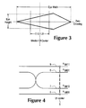
- the PCIE 3.0 specification requires that a DFE adaption method identify an optimal value for the feedback coefficient d 1 so that the eye height V eye and eye width of a signal, as displayed on an oscilloscope for example, are maximized.
- V eye is measured from the maximum of bit 0's and minimum of bit 1's, evaluated at a specified horizontal position of the unit interval (UI), usually, around UI center, as illustrated in FIG 3 .
- UI unit interval
- a DFE uses a training sequence which may sometimes also be referred to as a "decision bit” sequence. Because of this a DFE may be characterized as using a "decision on previous bits" to determine a coefficient feedback value. As is known in the art, in accordance with PCIE 3.0 when optimal tap values are identified, the tap values remain unchanged unless the channel or transmitter is changed. Thus, in accordance with embodiments of the present invention once optimal tap values are identified they may be used to identify all of the components of an analog waveform input signal (or bits of its digitized version) that need to be adjusted to account for signal degradations.
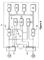
- the input signal can be associated with one of four 2-bit combinations, such as the combination denoted by points 6-9 in FIGURE 4 , according to the identified sequence.
- the combinations may then be used to generate and display a shifted eye diagram as shown, for example, in FIG 4 on a performance oscilloscope.
- the probe 440 may comprise a control box connected to the oscilloscope and a probe head coupled by a signal cable to the control box.
- the probe 440 may be coupled to the text fixture 460 using probing contacts.
- the oscilloscope 400 may include a display device 520 which may include a graphical user interface for displaying signals processed by the oscilloscope 400 from DUT 460.
- oscilloscope 400 may include front panel controls 540, such as rotatable knobs, push buttons and the like for controlling the settings of the oscilloscope.
- the front panel controls may be graphically generated and presented as so called "soft keys" on the display section 520 so as to be accessed by a user of the oscilloscope 400.
- a power supply 780 may receive control signals from the processing means 660 for controlling the electrical power to the probes 440 via voltage lines 800 and the accessory interfaces 420.
- sampled input signal may, or may not, have been output from a CTLE. If no CTLE is involved the input signal may be output from a channel or signal source.
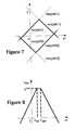
- the eye height V eye set forth in equation (3) can then be derived as function of d 1 based on FIGURE 7 and equation (6).
- this may be implemented using the processor 660 that is operable to access and execute stored instructions and data within memory means 700 for identifying a maximum voltage value representing a maximum eye height based on the generated voltage array output values.
- the processor 660 may be further operable to access and execute stored instructions and data from memory means 700 in order to generate a non-linear, equalized output signal ( y k ) based on the one or more identified, optimum feedback coefficient values.
- the processor 660 in effect, completes a DFE adaption process by identifying one or more optimum feedback coefficient values based on an identified, maximum voltage value, wherein the identified maximum voltage value is associated with a specified horizontal position of the UI by virtue of the inter-relationship of the UI and the steps involved in identifying the maximum voltage value.
- instructions and data for implementing such a process may be stored in memory means 700.
- the processor 660 may, optionally, access executable instructions and data (e.g., digitized signal samples of waveform x) from memory means 700 to generate a continuous, linearly equalized signal using an optional CTLE module within the processor 660 prior to a DFE adaption process.
- FIGURES 10A and B depict vertical histograms at UI center before and after DFE, respectively, as displayed on an oscilloscope such as system 400. As shown in these FIGUREs DFE adaption makes the eye open wider.
- FIGURE 11 there is depicted a user interface 900 that may be part of a performance oscilloscope for activating an optimum DFE process according an embodiment of the present invention.
- the user interface 900 may be part of the display section 520.
- an activation icon 920 may be displayed on the interface 900 which when clicked with a mouse, touched with a finger or otherwise activated begins the process of executing the DFE adaption process(es) for a high speed serial data signal of at least 6 gigabits per second described above.
- a save icon 1102 may be selected to (e.g., clicked, touched) to save the results of a DFE adaption process, for example in memory means 700.
- Equation (12) can be converted to a linear programming problem or equation to perform the optimization.
- Equation (15) shows a standard form of a linear program: m ⁇ i ⁇ n z f T z such that ⁇ A ⁇ z ⁇ b l ⁇ b ⁇ z ⁇ u ⁇ b
- f, z, b, lb, and ub are vectors, and A is a matrix.
- bit111, bit011, bit101, bit001 all have the last bit being one, while the four bit patterns bit110, bit010, bit100, bit000 all have the last bit being zero.
- the maximum of every one of the four bit patterns bit110, bit010, bit100, bit000 will be subtracted from the minimum of every one of the four bit patterns bit111, bit011, bit101, bit001.
- equation (17) can be re-written as Veye - x bit ⁇ 111 min - d 1 - d 2 + x bit ⁇ 110 max - d 1 - d 2 ⁇ 0
- Equation (18) can then be written as shown in equation (19): 1 0 0 z ⁇ x bit ⁇ 111 min - x bit ⁇ 110 max
- Equations (21), (22), and (23) fully construct the DFE optimization problem into a standard linear programming problem format for equation (12).
- An efficient linear programming solver such as Matlab (RTM), is used to find the optimal DFE feedback coefficient values d 1 and d 2 .
- equations (12), (21), (22), and (23) are derived based on a two-feedback coefficient DFE scenario.
- the same idea can be used for any multi-feedback coefficient DFE case, such as for a three-feedback coefficient case or a four-feedback coefficient case.
- the combination of minimums of n+1 bit patterns ending with bit 1 and maximums of n+1-bit patterns ending with bit 0 will be total of 4 n .
- the actual computation complexity is lower since many of the inequalities can be detected as trivial conditions.
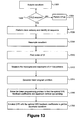
- FIGURE 13 depicts a flow diagram summarizing the methods set forth above that optimize a DFE according to embodiments of the present invention. Initially, a waveform is acquired in 1300 and then CTLE is performed in 1304, if required in 1302. In 1306, a clock recovery is performed and a bit sequence is identified from the digitized samples of the input signal.
- the DFE adaptation module figures out the bit sequence after clock recovery. To begin with, a one-feedback coefficient DFE is considered.
- V eye 40.2mV.
- V eye 43.92mV. This results in about a 10% increase in the vertical eye opening compared to a one-feedback coefficient DFE.
- FIGURE 14A depicts the eye opening before a DFE adaptation process
- FIGURE 14B depicts the eye opening after the DFE adaptation process.
- An example embodiment may provide a system (and corresponding method) for optimizing the equalization of a high-speed data link, comprising an input configured to receive an input waveform, a processor configured to perform decision feedback equalizer (DFE) adaptation on the input waveform for a multi-feedback coefficient DFE with n feedback coefficients, where n is greater than 1, the processor operable to execute stored instructions, including measuring minimum and maximum voltage outputs associated with a specified horizontal position of the unit interval for n+1 bit patterns for the input waveform, formulating a linear equation using the measured minimum and maximum voltage outputs of the n+1 bit patterns, determining the optimal n feedback coefficients by solving the linear equation, and emulating the DFE to determine an equalized input waveform based on the determined optimal n feedback coefficients.
- DFE decision feedback equalizer
- An example embodiment may provide a system (and corresponding method) for optimizing equalization of a high-speed data link comprising an input configured to receive an input waveform, a processor configured to perform multi-feedback coefficient decision feedback, equalization (DFE) adaptation on the input waveform using n feedback coefficients, where n is greater than 1, the processor configured to:measure minimum and maximum voltage outputs associated with a specified horizontal position of a unit interval for n+1 bit patterns for the input waveform; determine optimal n feedback coefficients using the measured minimum and maximum voltage outputs; and generate and output a non-linear, equalized signal by applying the determined optimal n feedback coefficients to the input waveform, wherein the optimal n feedback coefficients are determined by: m ⁇ i ⁇ n z f T z such that ⁇ A ⁇ z ⁇ b l ⁇ b ⁇ z ⁇ u ⁇ b where f, z, b, lb, and ub are vectors and A is a matrix, wherein each
Landscapes
- Engineering & Computer Science (AREA)
- Power Engineering (AREA)
- Computer Networks & Wireless Communication (AREA)
- Signal Processing (AREA)
- Dc Digital Transmission (AREA)
- Cable Transmission Systems, Equalization Of Radio And Reduction Of Echo (AREA)
- Filters That Use Time-Delay Elements (AREA)
Applications Claiming Priority (2)
| Application Number | Priority Date | Filing Date | Title |
|---|---|---|---|
| US201462026408P | 2014-07-18 | 2014-07-18 | |
| US14/468,553 US9191245B2 (en) | 2011-03-08 | 2014-08-26 | Methods and systems for providing optimum decision feedback equalization of high-speed serial data links |
Publications (2)
| Publication Number | Publication Date |
|---|---|
| EP2975813A1 true EP2975813A1 (de) | 2016-01-20 |
| EP2975813B1 EP2975813B1 (de) | 2018-12-26 |
Family
ID=53761196
Family Applications (1)
| Application Number | Title | Priority Date | Filing Date |
|---|---|---|---|
| EP15177328.0A Active EP2975813B1 (de) | 2014-07-18 | 2015-07-17 | Verfahren und systeme zur bereitstellung von optimaler entscheidungsrückkopplungsentzerrung von seriellen hochgeschwindigkeits-datenverbindungen |
Country Status (3)
| Country | Link |
|---|---|
| EP (1) | EP2975813B1 (de) |
| JP (1) | JP6671877B2 (de) |
| CN (1) | CN105282065B (de) |
Families Citing this family (2)
| Publication number | Priority date | Publication date | Assignee | Title |
|---|---|---|---|---|
| JP7558642B2 (ja) * | 2018-02-05 | 2024-10-01 | テクトロニクス・インコーポレイテッド | ノイズ・フィルタ及びノイズ低減方法 |
| JP2019169827A (ja) | 2018-03-23 | 2019-10-03 | 東芝メモリ株式会社 | イコライザ回路及びイコライザ回路の制御方法 |
Citations (3)
| Publication number | Priority date | Publication date | Assignee | Title |
|---|---|---|---|---|
| US20120320964A1 (en) * | 2011-03-08 | 2012-12-20 | Tektronix, Inc. | Methods and systems for providing optimum decision feedback equalization of high-speed serial data links |
| US8374231B2 (en) | 2008-04-30 | 2013-02-12 | Tektronix, Inc. | Equalization simulator with training sequence detection for an oscilloscope |
| US20140181339A1 (en) * | 2012-12-20 | 2014-06-26 | Nvidia Corporation | Equalization coefficient search algorithm |
Family Cites Families (5)
| Publication number | Priority date | Publication date | Assignee | Title |
|---|---|---|---|---|
| CN100521524C (zh) * | 2002-12-09 | 2009-07-29 | 飞思卡尔半导体公司 | 判决前馈均衡器系统和方法 |
| US7443914B2 (en) * | 2004-10-27 | 2008-10-28 | Yehuda Azenkot | DFE to FFE equalization coefficient conversion process for DOCSIS 2.0 |
| US7746969B2 (en) * | 2006-03-28 | 2010-06-29 | Entropic Communications, Inc. | High definition multi-media interface |
| JP4956840B2 (ja) * | 2008-03-14 | 2012-06-20 | 日本電気株式会社 | 判定帰還等化装置及び方法 |
| US10073750B2 (en) * | 2012-06-11 | 2018-09-11 | Tektronix, Inc. | Serial data link measurement and simulation system |
-
2015
- 2015-07-17 CN CN201510426653.0A patent/CN105282065B/zh active Active
- 2015-07-17 JP JP2015143375A patent/JP6671877B2/ja active Active
- 2015-07-17 EP EP15177328.0A patent/EP2975813B1/de active Active
Patent Citations (3)
| Publication number | Priority date | Publication date | Assignee | Title |
|---|---|---|---|---|
| US8374231B2 (en) | 2008-04-30 | 2013-02-12 | Tektronix, Inc. | Equalization simulator with training sequence detection for an oscilloscope |
| US20120320964A1 (en) * | 2011-03-08 | 2012-12-20 | Tektronix, Inc. | Methods and systems for providing optimum decision feedback equalization of high-speed serial data links |
| US20140181339A1 (en) * | 2012-12-20 | 2014-06-26 | Nvidia Corporation | Equalization coefficient search algorithm |
Non-Patent Citations (2)
| Title |
|---|
| JIHONG REN, MARK GREENSTREET: "A Unified Optimization Framework for Equalization FIlter Synthesis", ACM, 2 PENN PLAZA, SUITE 701 - NEW YORK USA, 13 June 2005 (2005-06-13) - 17 June 2005 (2005-06-17), Anaheim, California, USA, pages 638 - 643, XP040020520 * |
| KAN TAN: "DFE Adaptation Method for PCIe 8GT/s Testing", PCI-SIG, 1 January 2011 (2011-01-01), pages 1 - 22, XP002750732, Retrieved from the Internet <URL:http://kavi.pcisig.com/developers/main/training_materials/get_document?doc_id=1e27758ac315995bb0de2862a6e7ebbe0251a523> [retrieved on 20151110] * |
Also Published As
| Publication number | Publication date |
|---|---|
| CN105282065A (zh) | 2016-01-27 |
| CN105282065B (zh) | 2020-09-15 |
| EP2975813B1 (de) | 2018-12-26 |
| JP6671877B2 (ja) | 2020-03-25 |
| JP2016025662A (ja) | 2016-02-08 |
Similar Documents
| Publication | Publication Date | Title |
|---|---|---|
| US9191245B2 (en) | Methods and systems for providing optimum decision feedback equalization of high-speed serial data links | |
| US8855186B2 (en) | Methods and systems for providing optimum decision feedback equalization of high-speed serial data links | |
| EP2113775B1 (de) | Ausgleichssimulator mit Übungssequenzerfassung für ein Oszilloskop | |
| US11907090B2 (en) | Machine learning for taps to accelerate TDECQ and other measurements | |
| CN107770107B (zh) | 测试和测量系统以及在测试和测量系统中采用dfe的方法 | |
| CN112448760B (zh) | 一种获取发射机测试参数的方法和装置以及存储介质 | |
| CN115378773A (zh) | 用于测量的基于短模式波形数据库的机器学习 | |
| US11940889B2 (en) | Combined TDECQ measurement and transmitter tuning using machine learning | |
| US11765002B2 (en) | Explicit solution for DFE optimization with constraints | |
| US7693691B1 (en) | Systems and methods for simulating link performance | |
| EP2975813B1 (de) | Verfahren und systeme zur bereitstellung von optimaler entscheidungsrückkopplungsentzerrung von seriellen hochgeschwindigkeits-datenverbindungen | |
| JP2018159702A (ja) | 試験測定システム、波形処理方法及びコンピュータ・プログラム | |
| US8223830B2 (en) | Method and apparatus for determining equalization coefficients | |
| US11038768B1 (en) | Method and system for correlation of a behavioral model to a circuit realization for a communications system | |
| US9673862B1 (en) | System and method of analyzing crosstalk without measuring aggressor signal | |
| JP2024001002A (ja) | 試験測定装置及び測定方法 | |
| TW202413957A (zh) | 分離雜訊以增加測試及測量系統中的機器學習預測準確度 | |
| KR20200075342A (ko) | 신호 카운팅 방식 기반의 눈 열림 모니터를 이용한 샘플링 포인트 컨트롤러 | |
| CN1983832A (zh) | 一种确定滤波器系数的方法和系统 | |
| US8687683B2 (en) | Method of optimizing floating DFE receiver taps | |
| US20230204629A1 (en) | Method of ctle estimation using channel step-response for transmitter link equalization test | |
| JP2023098859A (ja) | Ctleフィルタの自動選択方法及び試験測定装置 | |
| CN117273164A (zh) | 用于使用从波形提取的线性响应进行测量的机器学习 | |
| US20250004014A1 (en) | Multiple pulse extraction for transmitter calibration | |
| Tsiklauri et al. | S-parameters quality estimation in physical units |
Legal Events
| Date | Code | Title | Description |
|---|---|---|---|
| PUAI | Public reference made under article 153(3) epc to a published international application that has entered the european phase |
Free format text: ORIGINAL CODE: 0009012 |
|
| AK | Designated contracting states |
Kind code of ref document: A1 Designated state(s): AL AT BE BG CH CY CZ DE DK EE ES FI FR GB GR HR HU IE IS IT LI LT LU LV MC MK MT NL NO PL PT RO RS SE SI SK SM TR |
|
| AX | Request for extension of the european patent |
Extension state: BA ME |
|
| 17P | Request for examination filed |
Effective date: 20160707 |
|
| RBV | Designated contracting states (corrected) |
Designated state(s): AL AT BE BG CH CY CZ DE DK EE ES FI FR GB GR HR HU IE IS IT LI LT LU LV MC MK MT NL NO PL PT RO RS SE SI SK SM TR |
|
| RIC1 | Information provided on ipc code assigned before grant |
Ipc: H04L 25/03 20060101AFI20180524BHEP |
|
| GRAP | Despatch of communication of intention to grant a patent |
Free format text: ORIGINAL CODE: EPIDOSNIGR1 |
|
| STAA | Information on the status of an ep patent application or granted ep patent |
Free format text: STATUS: GRANT OF PATENT IS INTENDED |
|
| INTG | Intention to grant announced |
Effective date: 20180705 |
|
| GRAS | Grant fee paid |
Free format text: ORIGINAL CODE: EPIDOSNIGR3 |
|
| GRAA | (expected) grant |
Free format text: ORIGINAL CODE: 0009210 |
|
| STAA | Information on the status of an ep patent application or granted ep patent |
Free format text: STATUS: THE PATENT HAS BEEN GRANTED |
|
| AK | Designated contracting states |
Kind code of ref document: B1 Designated state(s): AL AT BE BG CH CY CZ DE DK EE ES FI FR GB GR HR HU IE IS IT LI LT LU LV MC MK MT NL NO PL PT RO RS SE SI SK SM TR |
|
| REG | Reference to a national code |
Ref country code: GB Ref legal event code: FG4D |
|
| REG | Reference to a national code |
Ref country code: CH Ref legal event code: EP |
|
| REG | Reference to a national code |
Ref country code: AT Ref legal event code: REF Ref document number: 1082941 Country of ref document: AT Kind code of ref document: T Effective date: 20190115 |
|
| REG | Reference to a national code |
Ref country code: DE Ref legal event code: R096 Ref document number: 602015022148 Country of ref document: DE |
|
| REG | Reference to a national code |
Ref country code: IE Ref legal event code: FG4D |
|
| PG25 | Lapsed in a contracting state [announced via postgrant information from national office to epo] |
Ref country code: BG Free format text: LAPSE BECAUSE OF FAILURE TO SUBMIT A TRANSLATION OF THE DESCRIPTION OR TO PAY THE FEE WITHIN THE PRESCRIBED TIME-LIMIT Effective date: 20190326 Ref country code: LT Free format text: LAPSE BECAUSE OF FAILURE TO SUBMIT A TRANSLATION OF THE DESCRIPTION OR TO PAY THE FEE WITHIN THE PRESCRIBED TIME-LIMIT Effective date: 20181226 Ref country code: NO Free format text: LAPSE BECAUSE OF FAILURE TO SUBMIT A TRANSLATION OF THE DESCRIPTION OR TO PAY THE FEE WITHIN THE PRESCRIBED TIME-LIMIT Effective date: 20190326 Ref country code: LV Free format text: LAPSE BECAUSE OF FAILURE TO SUBMIT A TRANSLATION OF THE DESCRIPTION OR TO PAY THE FEE WITHIN THE PRESCRIBED TIME-LIMIT Effective date: 20181226 Ref country code: HR Free format text: LAPSE BECAUSE OF FAILURE TO SUBMIT A TRANSLATION OF THE DESCRIPTION OR TO PAY THE FEE WITHIN THE PRESCRIBED TIME-LIMIT Effective date: 20181226 Ref country code: FI Free format text: LAPSE BECAUSE OF FAILURE TO SUBMIT A TRANSLATION OF THE DESCRIPTION OR TO PAY THE FEE WITHIN THE PRESCRIBED TIME-LIMIT Effective date: 20181226 |
|
| REG | Reference to a national code |
Ref country code: NL Ref legal event code: MP Effective date: 20181226 |
|
| REG | Reference to a national code |
Ref country code: LT Ref legal event code: MG4D |
|
| PG25 | Lapsed in a contracting state [announced via postgrant information from national office to epo] |
Ref country code: SE Free format text: LAPSE BECAUSE OF FAILURE TO SUBMIT A TRANSLATION OF THE DESCRIPTION OR TO PAY THE FEE WITHIN THE PRESCRIBED TIME-LIMIT Effective date: 20181226 Ref country code: AL Free format text: LAPSE BECAUSE OF FAILURE TO SUBMIT A TRANSLATION OF THE DESCRIPTION OR TO PAY THE FEE WITHIN THE PRESCRIBED TIME-LIMIT Effective date: 20181226 Ref country code: GR Free format text: LAPSE BECAUSE OF FAILURE TO SUBMIT A TRANSLATION OF THE DESCRIPTION OR TO PAY THE FEE WITHIN THE PRESCRIBED TIME-LIMIT Effective date: 20190327 Ref country code: RS Free format text: LAPSE BECAUSE OF FAILURE TO SUBMIT A TRANSLATION OF THE DESCRIPTION OR TO PAY THE FEE WITHIN THE PRESCRIBED TIME-LIMIT Effective date: 20181226 |
|
| REG | Reference to a national code |
Ref country code: AT Ref legal event code: MK05 Ref document number: 1082941 Country of ref document: AT Kind code of ref document: T Effective date: 20181226 |
|
| PG25 | Lapsed in a contracting state [announced via postgrant information from national office to epo] |
Ref country code: NL Free format text: LAPSE BECAUSE OF FAILURE TO SUBMIT A TRANSLATION OF THE DESCRIPTION OR TO PAY THE FEE WITHIN THE PRESCRIBED TIME-LIMIT Effective date: 20181226 |
|
| PG25 | Lapsed in a contracting state [announced via postgrant information from national office to epo] |
Ref country code: CZ Free format text: LAPSE BECAUSE OF FAILURE TO SUBMIT A TRANSLATION OF THE DESCRIPTION OR TO PAY THE FEE WITHIN THE PRESCRIBED TIME-LIMIT Effective date: 20181226 Ref country code: IT Free format text: LAPSE BECAUSE OF FAILURE TO SUBMIT A TRANSLATION OF THE DESCRIPTION OR TO PAY THE FEE WITHIN THE PRESCRIBED TIME-LIMIT Effective date: 20181226 Ref country code: PL Free format text: LAPSE BECAUSE OF FAILURE TO SUBMIT A TRANSLATION OF THE DESCRIPTION OR TO PAY THE FEE WITHIN THE PRESCRIBED TIME-LIMIT Effective date: 20181226 Ref country code: ES Free format text: LAPSE BECAUSE OF FAILURE TO SUBMIT A TRANSLATION OF THE DESCRIPTION OR TO PAY THE FEE WITHIN THE PRESCRIBED TIME-LIMIT Effective date: 20181226 Ref country code: PT Free format text: LAPSE BECAUSE OF FAILURE TO SUBMIT A TRANSLATION OF THE DESCRIPTION OR TO PAY THE FEE WITHIN THE PRESCRIBED TIME-LIMIT Effective date: 20190426 |
|
| PG25 | Lapsed in a contracting state [announced via postgrant information from national office to epo] |
Ref country code: EE Free format text: LAPSE BECAUSE OF FAILURE TO SUBMIT A TRANSLATION OF THE DESCRIPTION OR TO PAY THE FEE WITHIN THE PRESCRIBED TIME-LIMIT Effective date: 20181226 Ref country code: SM Free format text: LAPSE BECAUSE OF FAILURE TO SUBMIT A TRANSLATION OF THE DESCRIPTION OR TO PAY THE FEE WITHIN THE PRESCRIBED TIME-LIMIT Effective date: 20181226 Ref country code: IS Free format text: LAPSE BECAUSE OF FAILURE TO SUBMIT A TRANSLATION OF THE DESCRIPTION OR TO PAY THE FEE WITHIN THE PRESCRIBED TIME-LIMIT Effective date: 20190426 Ref country code: RO Free format text: LAPSE BECAUSE OF FAILURE TO SUBMIT A TRANSLATION OF THE DESCRIPTION OR TO PAY THE FEE WITHIN THE PRESCRIBED TIME-LIMIT Effective date: 20181226 Ref country code: SK Free format text: LAPSE BECAUSE OF FAILURE TO SUBMIT A TRANSLATION OF THE DESCRIPTION OR TO PAY THE FEE WITHIN THE PRESCRIBED TIME-LIMIT Effective date: 20181226 |
|
| REG | Reference to a national code |
Ref country code: DE Ref legal event code: R097 Ref document number: 602015022148 Country of ref document: DE |
|
| PG25 | Lapsed in a contracting state [announced via postgrant information from national office to epo] |
Ref country code: AT Free format text: LAPSE BECAUSE OF FAILURE TO SUBMIT A TRANSLATION OF THE DESCRIPTION OR TO PAY THE FEE WITHIN THE PRESCRIBED TIME-LIMIT Effective date: 20181226 Ref country code: DK Free format text: LAPSE BECAUSE OF FAILURE TO SUBMIT A TRANSLATION OF THE DESCRIPTION OR TO PAY THE FEE WITHIN THE PRESCRIBED TIME-LIMIT Effective date: 20181226 |
|
| PLBE | No opposition filed within time limit |
Free format text: ORIGINAL CODE: 0009261 |
|
| STAA | Information on the status of an ep patent application or granted ep patent |
Free format text: STATUS: NO OPPOSITION FILED WITHIN TIME LIMIT |
|
| 26N | No opposition filed |
Effective date: 20190927 |
|
| PG25 | Lapsed in a contracting state [announced via postgrant information from national office to epo] |
Ref country code: MC Free format text: LAPSE BECAUSE OF FAILURE TO SUBMIT A TRANSLATION OF THE DESCRIPTION OR TO PAY THE FEE WITHIN THE PRESCRIBED TIME-LIMIT Effective date: 20181226 Ref country code: SI Free format text: LAPSE BECAUSE OF FAILURE TO SUBMIT A TRANSLATION OF THE DESCRIPTION OR TO PAY THE FEE WITHIN THE PRESCRIBED TIME-LIMIT Effective date: 20181226 |
|
| REG | Reference to a national code |
Ref country code: CH Ref legal event code: PL |
|
| GBPC | Gb: european patent ceased through non-payment of renewal fee |
Effective date: 20190717 |
|
| PG25 | Lapsed in a contracting state [announced via postgrant information from national office to epo] |
Ref country code: TR Free format text: LAPSE BECAUSE OF FAILURE TO SUBMIT A TRANSLATION OF THE DESCRIPTION OR TO PAY THE FEE WITHIN THE PRESCRIBED TIME-LIMIT Effective date: 20181226 |
|
| REG | Reference to a national code |
Ref country code: BE Ref legal event code: MM Effective date: 20190731 |
|
| PG25 | Lapsed in a contracting state [announced via postgrant information from national office to epo] |
Ref country code: GB Free format text: LAPSE BECAUSE OF NON-PAYMENT OF DUE FEES Effective date: 20190717 |
|
| PG25 | Lapsed in a contracting state [announced via postgrant information from national office to epo] |
Ref country code: LI Free format text: LAPSE BECAUSE OF NON-PAYMENT OF DUE FEES Effective date: 20190731 Ref country code: BE Free format text: LAPSE BECAUSE OF NON-PAYMENT OF DUE FEES Effective date: 20190731 Ref country code: CH Free format text: LAPSE BECAUSE OF NON-PAYMENT OF DUE FEES Effective date: 20190731 Ref country code: LU Free format text: LAPSE BECAUSE OF NON-PAYMENT OF DUE FEES Effective date: 20190717 |
|
| PG25 | Lapsed in a contracting state [announced via postgrant information from national office to epo] |
Ref country code: FR Free format text: LAPSE BECAUSE OF NON-PAYMENT OF DUE FEES Effective date: 20190731 |
|
| PG25 | Lapsed in a contracting state [announced via postgrant information from national office to epo] |
Ref country code: IE Free format text: LAPSE BECAUSE OF NON-PAYMENT OF DUE FEES Effective date: 20190717 |
|
| PG25 | Lapsed in a contracting state [announced via postgrant information from national office to epo] |
Ref country code: CY Free format text: LAPSE BECAUSE OF FAILURE TO SUBMIT A TRANSLATION OF THE DESCRIPTION OR TO PAY THE FEE WITHIN THE PRESCRIBED TIME-LIMIT Effective date: 20181226 |
|
| PG25 | Lapsed in a contracting state [announced via postgrant information from national office to epo] |
Ref country code: MT Free format text: LAPSE BECAUSE OF FAILURE TO SUBMIT A TRANSLATION OF THE DESCRIPTION OR TO PAY THE FEE WITHIN THE PRESCRIBED TIME-LIMIT Effective date: 20181226 Ref country code: HU Free format text: LAPSE BECAUSE OF FAILURE TO SUBMIT A TRANSLATION OF THE DESCRIPTION OR TO PAY THE FEE WITHIN THE PRESCRIBED TIME-LIMIT; INVALID AB INITIO Effective date: 20150717 |
|
| PG25 | Lapsed in a contracting state [announced via postgrant information from national office to epo] |
Ref country code: MK Free format text: LAPSE BECAUSE OF FAILURE TO SUBMIT A TRANSLATION OF THE DESCRIPTION OR TO PAY THE FEE WITHIN THE PRESCRIBED TIME-LIMIT Effective date: 20181226 |
|
| P01 | Opt-out of the competence of the unified patent court (upc) registered |
Effective date: 20230530 |
|
| PGFP | Annual fee paid to national office [announced via postgrant information from national office to epo] |
Ref country code: DE Payment date: 20250729 Year of fee payment: 11 |