EP2975423A1 - Dispositif de mesure de magnétisme - Google Patents
Dispositif de mesure de magnétisme Download PDFInfo
- Publication number
- EP2975423A1 EP2975423A1 EP14760217.1A EP14760217A EP2975423A1 EP 2975423 A1 EP2975423 A1 EP 2975423A1 EP 14760217 A EP14760217 A EP 14760217A EP 2975423 A1 EP2975423 A1 EP 2975423A1
- Authority
- EP
- European Patent Office
- Prior art keywords
- magnetic
- measuring device
- amorphous
- field measuring
- amorphous material
- Prior art date
- Legal status (The legal status is an assumption and is not a legal conclusion. Google has not performed a legal analysis and makes no representation as to the accuracy of the status listed.)
- Granted
Links
- 238000005259 measurement Methods 0.000 title abstract description 11
- 230000005389 magnetism Effects 0.000 title abstract description 10
- 239000000463 material Substances 0.000 claims abstract description 134
- 239000007788 liquid Substances 0.000 claims abstract description 11
- 239000007787 solid Substances 0.000 claims abstract description 7
- 239000004020 conductor Substances 0.000 claims description 63
- 239000000696 magnetic material Substances 0.000 claims description 47
- 230000005415 magnetization Effects 0.000 claims description 37
- 239000002131 composite material Substances 0.000 claims description 7
- 230000001939 inductive effect Effects 0.000 abstract 1
- 239000000523 sample Substances 0.000 description 40
- 238000012545 processing Methods 0.000 description 17
- 230000035945 sensitivity Effects 0.000 description 14
- 238000001514 detection method Methods 0.000 description 12
- 230000008901 benefit Effects 0.000 description 11
- 230000008859 change Effects 0.000 description 11
- 230000008878 coupling Effects 0.000 description 6
- 238000010168 coupling process Methods 0.000 description 6
- 238000005859 coupling reaction Methods 0.000 description 6
- 238000002474 experimental method Methods 0.000 description 5
- 238000000034 method Methods 0.000 description 4
- 230000001052 transient effect Effects 0.000 description 4
- 230000003321 amplification Effects 0.000 description 3
- 238000006243 chemical reaction Methods 0.000 description 3
- 238000009826 distribution Methods 0.000 description 3
- 230000005281 excited state Effects 0.000 description 3
- 239000010408 film Substances 0.000 description 3
- 238000003199 nucleic acid amplification method Methods 0.000 description 3
- 238000005476 soldering Methods 0.000 description 3
- 230000008602 contraction Effects 0.000 description 2
- 230000007423 decrease Effects 0.000 description 2
- 238000006073 displacement reaction Methods 0.000 description 2
- 230000000694 effects Effects 0.000 description 2
- 230000033001 locomotion Effects 0.000 description 2
- 230000004048 modification Effects 0.000 description 2
- 238000012986 modification Methods 0.000 description 2
- 230000008569 process Effects 0.000 description 2
- 239000010409 thin film Substances 0.000 description 2
- 230000005668 Josephson effect Effects 0.000 description 1
- 230000000747 cardiac effect Effects 0.000 description 1
- 230000006866 deterioration Effects 0.000 description 1
- 230000002500 effect on skin Effects 0.000 description 1
- 239000012777 electrically insulating material Substances 0.000 description 1
- 230000008030 elimination Effects 0.000 description 1
- 238000003379 elimination reaction Methods 0.000 description 1
- 230000006872 improvement Effects 0.000 description 1
- 238000009413 insulation Methods 0.000 description 1
- 238000004519 manufacturing process Methods 0.000 description 1
- 238000005457 optimization Methods 0.000 description 1
- 239000002245 particle Substances 0.000 description 1
- 230000035699 permeability Effects 0.000 description 1
- 238000011160 research Methods 0.000 description 1
- 230000002269 spontaneous effect Effects 0.000 description 1
- 238000003860 storage Methods 0.000 description 1
- 238000003466 welding Methods 0.000 description 1
- 238000004804 winding Methods 0.000 description 1
Images


Classifications
-
- G—PHYSICS
- G01—MEASURING; TESTING
- G01R—MEASURING ELECTRIC VARIABLES; MEASURING MAGNETIC VARIABLES
- G01R33/00—Arrangements or instruments for measuring magnetic variables
- G01R33/02—Measuring direction or magnitude of magnetic fields or magnetic flux
-
- G—PHYSICS
- G01—MEASURING; TESTING
- G01R—MEASURING ELECTRIC VARIABLES; MEASURING MAGNETIC VARIABLES
- G01R33/00—Arrangements or instruments for measuring magnetic variables
- G01R33/0023—Electronic aspects, e.g. circuits for stimulation, evaluation, control; Treating the measured signals; calibration
- G01R33/0029—Treating the measured signals, e.g. removing offset or noise
-
- G—PHYSICS
- G01—MEASURING; TESTING
- G01R—MEASURING ELECTRIC VARIABLES; MEASURING MAGNETIC VARIABLES
- G01R33/00—Arrangements or instruments for measuring magnetic variables
- G01R33/02—Measuring direction or magnitude of magnetic fields or magnetic flux
- G01R33/028—Electrodynamic magnetometers
Definitions
- the present invention relates to a magnetic-field measuring device, and more particularly to a magnetic-field measuring device for detecting magnetism on the basis of a variation of a magnetic moment in a material having magnetic anisotropy.
- Magnetic-field measuring devices for measuring magnetism with high sensitivity on the order of picotesla or nanotesla.
- SQUID superconducting quantum interference element or device
- MI sensor magneto-impedance sensor
- the magnetic-field detecting device using the SQUID utilizes a superconducting Josephson effect and a superconducting coil, and has a problem of requirement for a large-scale device for maintaining the magnetic-field detecting device at an extremely low temperature to establish a superconducting state, and equipment for tightly shielding the magnetic-field detecting device from an ambient magnetic field.
- the magnetic-field sensing device using the MI sensor is a sensor utilizing a phenomenon that an impedance of the MI element varies, due to a skin effect, depending upon the frequency of an alternating current applied to the sensor, and accordingly has an advantage that the sensor does not require a large-scale device and equipment as required by the above-described magnetic-field detecting device using the SQUID.
- the MI sensor described above requires electrical connection of conductors to amorphous wires having magnetic anisotropy, for applying the alternating current to the amorphous wires.
- This electrical connection is made by a method such as soldering and ultrasonic welding, which involves heat application to and vibratory motions of the amorphous wires, causing thermal expansion and contraction and positional displacement of the amorphous wires, and consequent variation of tension of the amorphous wires, giving rise to deterioration of accuracy of detection of the magnetic field by the MI sensor.
- Fig. 12 is a view indicating a relationship between the tension of the amorphous wires and the sensitivity of the MI sensor, which was obtained by an experiment conducted by the present inventors.
- the tension of the amorphous wires is taken along the horizontal axis
- the sensitivity of the amorphous wires is taken along the vertical axis.
- the sensitivity of the amorphous wires decreases with an increase of their tension, that is, the sensitivity and the tension of the amorphous wires have a close relationship therebetween.
- the variation of the tension of the amorphous wires attached to the MI sensor is not negligible for assuring the desired performance of the MI sensor as the product.
- the MI sensor is a gradiometer (gradient magnetic-field detecting device) configured to detect the magnetic field on the basis of a difference between outputs of two sensors
- these two sensors should be produced so as to have the same degree of sensitivity.
- the present invention was made in view of the background art described above. It is therefore an object of the present invention to provide a magnetic-field measuring device which can be produced with a simpler arrangement using a magnetic material having magnetic anisotropy and which permits high accuracy of measurement of the magnetic field.
- the present inventors found that the magnetic material having magnetic anisotropy have different directions of internal magnetization when any external magnetic field is not applied to the magnetic material and when an external magnetic field in which a subject to be measured is present is applied to the magnetic material, and that the direction of magnetization of the magnetic material is aligned with a magnetic field which is induced by application of an electric current not smaller than a predetermined value to a conductor disposed adjacent to the magnetic material.
- the present invention was made based on these findings.
- a magnetic-field measuring device having: (a) a magnetic material formed of a solid or liquid having magnetic anisotropy, or a composite of the solid and liquid; (b) an electrically conductive body disposed adjacent to the above-described magnetic material, so as to give a current-induced magnetic-field vector having a component perpendicular to a direction of easy magnetization of the above-described magnetic material; and (c) a coil to detect a magnetic field.
- the magnetic-field measuring device is characterized by (d) repeatedly applying an electric current to said electrically conductive body, and (e) detecting an electromotive force generated by the above-described coil, and obtaining an output of the above-described coil as an output signal of the magnetic-field measuring device.
- the above-described magnetic material generates the magnetic field on the basis of the electric current applied to the electrically conductive body, and the generated magnetic field causes the above-described coil to generate the electromotive force.
- the magnetic field can be detected by measuring the electromotive force, so that it is not necessary to positively apply the electric current to the magnetic material. Since it is not necessary to apply the electric current to the magnetic material, the electrical connection of the magnetic material is not necessary, so that the magnetic-field measuring device does not suffer from influences of physical changes of the magnetic material due to generation of heat and vibratory motions.
- the above-described magnetic material is an amorphous material.
- the direction of magnetization of the amorphous material easily changes due to the magnetic field to be measured, and the magnetic field generated by application of the electric current to the electrically conductive body, whereby the electromotive force is easily generated by the coil in the magnetic fields. Accordingly, the magnetic field can be easily measured with a high degree of accuracy.
- the above-described electric current is a pulse current, a current a value of which intermittently changes in a predetermined pattern, or a current which is a composite of those two currents superimposed on each other.
- the amount of the electric current applied to the electrically conductive body intermittently changes, so that the magnetic field can be measured on the basis of a change of the electromotive force of the above-described coil in synchronization of the change of the amount of the applied electric current.
- the above-described magnetic material consists of at least one amorphous wire having the direction of easy magnetization parallel to its longitudinal direction
- the above-described electrically conductive body consists of at least one conductor wire.
- the above-described magnetic material and the above-described electrically conductive body are suitably arranged in the present magnetic-field measuring device.
- the above-described magnetic material has a symmetrical shape with respect to a straight line or plane of symmetry which passes a midpoint in its direction of easy magnetization, and which is perpendicular to the direction of easy magnetization
- the above-described coil consists of two coils which are disposed at respective positions which are symmetrical with each other with respect to the above-described line or plane of symmetry, (c) whereby the magnetic-field measuring device is provided with a gradiometer.
- the two coils are disposed symmetrically with each other with respect to the line or plane of symmetry of the magnetic material, so that an influence of the ambient magnetic field such as the terrestrial magnetic field can be effectively eliminated, whereby the accuracy of measurement of the magnetic-field measuring device provided with the gradiometer can be improved.
- the above-described magnetic material includes an amorphous material having magnetic anisotropy
- the above-described amorphous material consists of at least one layer surrounding the above-described electrically conductive body.
- the magnetic-field measuring device can be configured such that the amorphous material and the electrically conductive body are disposed adjacent to each other.
- the above-described magnetic material includes an elongate amorphous material having magnetic anisotropy
- the above-described elongate amorphous material consists of at least one cylindrical layer wound in a coil on the above-described electrically conductive body so as to surround the electrically conductive body.
- the magnetic-field measuring device can be configured such that the amorphous material and the electrically conductive body are disposed adjacent to each other.
- the above-described amorphous material and the above-described electrically conductive body are electrically insulated from each other.
- the magnetic field generated by the amorphous material is not influenced by the electric current flowing through the amorphous material.
- the amount of electric current flowing through the electrically conductive body is not so large as to influence the measurement of the magnetic field, however, the amorphous material and the electrically conductive body need not be electrically insulated from each other.
- Fig. 1 is the schematic view for explaining a magnetic-field measuring device 10 according to an embodiment of this invention.
- the magnetic-field measuring device 10 includes a probe portion 12 to detect magnetism, and a circuit portion 14 to drive the probe portion 12.
- the probe portion 12 provides a magnetic gradiometer, which includes to two magneto-sensors, as described below. The probe portion 12 will be described later.
- the circuit portion 14 has a clock portion 20, a power supply portion 21 and a pulse generator 22, which are configured to apply an electric current to conductive portions 42 and 44 of the probe portion 12 described below.
- the clock portion 20 is a CMOS IC, for instance, and is configured to generate a pulse signal at a predetermined time interval.
- the pulse generator 22 is configured to apply a intermittently varying electric current Ie to the conductive portions 42 and 44 of the probe portion 12, on the basis of the pulse signal generated by the above-indicated clock portion 20 and a line voltage of the power supply portion 21.
- the intermittently varying electric current Ie takes the form of a rectangular pulse wave, for instance.
- the circuit portion 14 has sample hold circuits 24 and 26 to detect induced electromotive forces Ecoil1 and Ecoil2 generated by coils 50, 52 of the probe portion 12 described below, a differential amplifier 28, a filter 30, an amplifier 32 and a filter 34.
- the sample hold circuits 24 and 26 detect peaks (peak values) of amplitude of the electromotive forces Ecoil1 and Ecoil2 of the coils 50 and 52.
- the above-indicated clock portion 20 applies a trigger signal to the sample hold circuits 24 and 26, so that the detection of the peak values by the sample hold circuits 24 and 26 takes place at predetermined points of time (phase) in synchronization with this trigger signal.
- the differential amplifier 28 generates an output representing a difference between the output values of the sample hold circuits 24 and 26.
- the probe portion 12 including the two magneto-sensors functions as a gradiometer.
- the filter 30 is configured to remove a high-frequency component and a low-frequency component from the output of the differential amplifier 28 (to operate as a high-pass filter and a low-pass filter), and to generate an output representative of only a predetermined frequency component.
- the amplifier 32 is configured to amplify the output signal of the filter 30 by 1000 times, for example, according to a predetermined offset voltage Offset.
- the filter 34 is configured to remove a high-frequency component and a low-frequency component from the output of the amplifier 32, and to generate an output representative of only a predetermined frequency component.
- the output signal of the filter 34 is sent to a monitor or any other display device, a recording device, or any other device.
- Fig. 2 is the view schematically showing a basic arrangement of the probe portion 12.
- the probe portion 12 provided according to the present embodiment includes sensors 36 and 38.
- the present magnetic-field measuring device 10 is provided with a gradiometer, wherein one of the sensors 36 and 38 serves as a sensor for measuring a magnetic field Bmes of the subject to be measured, while the other sensor serves as a reference sensor. For this reason, the two sensors 36 and 38 have the same arrangement.
- Each of the sensors 36 and 38 has a magnetic material in the form of an amorphous material 46, 48, an electrically conductive body in the form of a conductor wire 42, 44, and the coil 50, 52.
- the amorphous materials 46 and 48 are elongate amorphous wires.
- the conductor wires 42 and 44 are disposed adjacent to the respective amorphous materials 46 and 48 such that the conductor wires 42 and 44 extend parallel to the longitudinal direction of the amorphous materials 46 and 48.
- the coils 50 and 52 are solenoid coils defining inner spaces through which the amorphous materials 46 and 48 and the conductor wires 42 and 44 extend.
- the amorphous materials 46 and 48 and the conductor wires 42 and 44 are not held in electrical contact with each other, with an air gap or an electrically insulating material being interposed therebetween.
- the arrangement of the sensors is not limited to the one described above.
- the amorphous materials 46 and 48 need not take the form of rods shown in Fig.
- the amorphous materials 46 and 48 are elongate members.
- the positional relationship of the coils 50 and 52 with respect to the amorphous materials 46 and 48 and the conductor wires 42 and 44 is not limited to the above-described arrangement wherein the amorphous materials 46 and 48 and the conductor wires 42 and 44 extend through the inner spaces of the coils 50 and 52.
- the coils 50 and 52 may be otherwise positioned relative to the amorphous materials 46 and 48 and the conductor wires 42 and 44, as long as the coils 50 and 52 can generate electric currents induced by the amorphous materials 46 and 48.
- the sensors 36 and 38 are spaced apart from each other so that one of these two sensors detects the magnetic field Bmes of the subject, while the other sensor does not detect the magnetic field Bmes.
- Fig. 3 is the view for explaining an electrical arrangement of the sensors 36, 38.
- the pulse generator 22 shown in Fig. 1 applies a pulse current Ie to the conductor wires 42 and 44, and the electromotive forces Ecoil1 and Ecoil2 generated by the respective coils 50 and 52 are applied to the respective sample hold circuits 24 and 26.
- each of the sensors 36 and 38 used according to the present embodiment is referred to as an iPA sensor (induced para-magnetization alignment sensor) or an iPA sensor element.
- FIGs. 4 are views showing only the amorphous material 46, 48 and the conductor wire 42, 44 of each iPA sensor, and explaining distributions of a magnetic charge within the amorphous material 46, 48. Arrows in the figures schematically indicate directions of the magnetic charge within the amorphous material 46, 48.
- Fig. 4(a) indicates a non-magnetic-field state in which an external magnetic field is not applied to the iPA sensor, namely, a so-called control state S(0) in which only an ambient magnetic field is applied to the iPA sensor.
- Fig. 4(a) indicates a non-magnetic-field state in which an external magnetic field is not applied to the iPA sensor, namely, a so-called control state S(0) in which only an ambient magnetic field is applied to the iPA sensor.
- FIG. 4(b) indicates a state S(1) in which the magnetic field Bmes of the subject to be measured is applied to the iPA sensor, while Fig. 4(c) indicates a state S(e) in which a sufficient exciting electric current Ie is applied to the conductor wire 42, 44.
- the state of magnetization of the amorphous material 46, 48 changes due to minute external magnetic field or fields, for instance, from the state S(0) of Fig. 4(a) to the state S(1) of Fig. 4(b) .
- the direction of magnetization (Mam) of the amorphous material 46, 48 is perpendicular to its longitudinal direction.
- the orientation of a magnetic moment defining a direction of easy magnetization partially changes.
- a magnetic field Be is generated as indicated by broken lines in the same figure.
- a given amount of magnetization within the amorphous material 46, 48 is aligned with the direction of the magnetic field Be.
- the application of the exciting electric current Ie permits alignment of the magnetization, and causes generation of a transient magnetic field.
- the intensity of the above-indicated transient magnetic field generated as a result of alignment of the magnetization changes depending on the magnetic field before the application of the exciting electric current Ie, more specifically, depending on the state of magnetization of the amorphous material 46, 48 in that magnetic field.
- the intensity of the transient magnetic field generated when the amorphous wire 46, 48 is switched from the state S(0) to the state S(e), and that generated when the amorphous wire 46, 48 is switched from the state S(1) to the state S(e) are different from each other.
- the transient magnetic field thus generated by the amorphous wire 46, 48 is detected by the corresponding coil 50, 52, as a change of the electromotive force Ecoil1, Ecoil2.
- This change of the electromotive force represents a change of the magnetization of the amorphous material 46, 48 before and after the application of the exciting electric current Ie. Described more specifically, the amount of the change depends on the magnetic field applied to the amorphous wire 46, 48 before the application of the exciting electric current Ie. In the state S(0) of the amorphous wire 46, 48 before the application of the exciting electric current Ie, the amount of the change is represented by ⁇ Mam(S(e)) - Mam(S(0)) ⁇ / ⁇ t.
- the amount of the change is represented by ⁇ Mam(S(e)) - Mam (S(1)) ⁇ / ⁇ t.
- the change of the electromotive force Ecoil1, Ecoil2 of the coil 50, 52 reflects the magnetic field Bmes applied to the subject to be measured.
- the intensity of the magnetic field Bmes can be calculated on the basis of the change of the electromotive force Ecoil1, Ecoil 2. It is noted that the above-indicated value ⁇ t represents a length of time required for alignment of the direction of magnetization, which is on the order of nanoseconds, for example.
- the exciting electric current Ie is the pulse current
- a time period of an excited state in which the magnetization of the amorphous material 46, 48 is aligned by the application of the exciting electric current Ie, and a time period of a non-excited state in which the magnetization is in the original state without the application of the exciting electric current Ie are repeatedly established at a high frequency. Accordingly, it is possible to detect a difference between the electromotive forces induced by the coil 50, 52 in the time periods of the excited and non-excited states. Further, an average of a plurality of values of the difference obtained by repeating this detection may be calculated.
- the amount of the above-described exciting electric current Ie is determined to be large enough to permit alignment of the internal magnetization of the amorphous wire 46, 48 in the ambient magnetic field, namely, in the terrestrial magnetism in the normal room environment. Described more specifically, where the conductor wire 42, 44 linearly extends, as shown in Figs. 2-4 , an approximate value of the intensity of the induced magnetic field Be at a position adjacent to the conductor wire 42, 44 upon application of the exciting electric current Ie is represented by the following equation, according to the Ampere's law:
- the magnetic-field measuring device 10 has: the magnetic materials in the form of the amorphous materials 46 and 48 formed of a solid or liquid having magnetic anisotropy, or a composite of the solid and the liquid; the conductor wires 42 and 44 disposed adjacent to the amorphous wires 46 and 48, so as to give a current-induced magnetic-field vector having a component perpendicular to a direction of easy magnetization of the magnetic materials; and the coils 50 and 52 to detect the magnetic field.
- the magnetic-field measuring device 10 is configured to intermittently apply an electric current to the conductor wires 42 and 44, detect the electromotive forces generated by the coils 50 and 52, and obtain the outputs of the coils 50 and 52 as an output signal of the magnetic-field measuring device 10.
- the amorphous materials 46 and 48 generate the magnetic field on the basis of the electric current applied to the conductor wires 42 and 44, and the generated magnetic field causes the coils 50 and 52 to generate the electromotive forces.
- the direction of the easy magnetization is a direction in which the magnetic moment is easily oriented in the amorphous materials 46 and 48.
- the magnetic field can be detected by measuring the electromotive forces of the coils 50 and 52, so that it is not necessary to positively apply the electric current to the amorphous materials 46 and 48. Since it is not necessary to apply the electric current to the amorphous materials 46 and 48, the electrical connection of the amorphous materials 46 and 48 is not necessary, so that the magnetic-field measuring device 10 does not suffer from influences of physical changes of the amorphous materials 46 and 48 due to a soldering or similar operation.
- the present embodiment is further configured to employ the amorphous materials 46 and 48 as the magnetic materials, so that the direction of magnetization of the amorphous materials 46 and 48 easily changes due to the magnetic field to be measured, and the magnetic field generated by application of the electric current to the conductor wires 42 and 44, whereby the electromotive forces are easily generated by the coils 50 and 52 in the magnetic fields. Accordingly, the magnetic field can be easily measured with a high degree of accuracy.
- the present embodiment is also configured such that the electric current to be applied to the conductor wires 42 and 44 is a pulse current, a current a value of which intermittently changes in a predetermined pattern, or a current which is a composite of those two currents superimposed on each other. Accordingly, the amount of the electric current applied to the conductor wires 42 and 44 intermittently changes, so that the magnetic field can be measured on the basis of changes of the electromotive forces of the coils 50 and 52 in synchronization of the change of the amount of the applied electric current.
- the present embodiment is further configured such that the magnetic material consists of at least one amorphous wire 46, 48 having the direction of easy magnetization parallel to its longitudinal direction, and the electrically conductive body consists of at least one conductor wire 42, 44. Accordingly, the magnetic material and the electrically conductive body are suitably arranged in the present magnetic-field measuring device 10.
- Figs. 5 are the views for schematically explaining an arrangement of a sensor (iPA sensor) 136 used in the magnetic-field measuring device 10 according to another embodiment of the invention.
- Fig. 5(a) is the view for explaining an arrangement of the sensor 136
- Fig. 5(b) is a cross sectional view of the sensor 136 taken in a plane perpendicular to its longitudinal direction. This sensor 136 is used in place of the sensors 36 and 38 used in the preceding embodiment.
- the sensor 136 shown in Figs. 5 has substantially the same arrangement as the sensors 36, 38 in the first embodiment. Described more specifically, the sensor 136 has the magnetic material in the form of an amorphous material 146, the electrically conductive body in the form of the conductor wire 42, and the coil 50.
- the amorphous material 146 is an elongate amorphous wire.
- the conductor wire 42 is disposed adjacent to the amorphous material 146, and extends in the longitudinal direction of the amorphous material 146.
- the coil 50 is a solenoid coil defining an inner space through which the amorphous material 146 and the conductor wire 42 extend.
- the amorphous material 146 used in the sensor 136 of Figs. 5 consists of a plurality of (more precisely, four) amorphous material pieces 146a-146d.
- the present sensor 146 is different from the sensor 36, 38 in the first embodiment shown in Fig. 2 , which uses a single piece of amorphous material 46, 48.
- the amorphous material consists of the plurality of amorphous wires, which may have different shapes.
- the number and the shapes of the amorphous wires may be selected according to the required detection sensitivity of the magnetic-field measuring device 10. Described more specifically, the amorphous material illustrated in Figs. 5 consists of two amorphous material pieces 146a and 146c each having a circular cross sectional shape, and two amorphous material pieces 146b and 146d each having a square cross sectional shape.
- the amorphous material is not limited to this combination of the amorphous pieces.
- the amorphous material may include amorphous material pieces having a cross sectional shape other than the circular and square cross sectional shapes, and may consist of any number of amorphous material pieces having any combination of the cross sectional shapes, other than those of Figs. 5 . That is, the present invention in which an electric current is not positively applied to the amorphous materials 46, 146a-146d has an advantage that changes of the number and the cross sectional surface areas of the amorphous material pieces do not cause a decrease of the amount of the exciting electric current, or an increase of a sum of the electric current amounts.
- the sensor 136 according to the second embodiment has substantially the same advantages as described above with respect to the first embodiment.
- the sensor 136 has an additional advantage that the sensitivity of the sensor 136 can be selected depending upon the number and the cross sectional shapes of the pieces of the amorphous material 146.
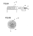
- Figs. 6 are the views for schematically explaining an arrangement of a sensor (iPA sensor) 236 used in the magnetic-field measuring device 10 according to a further embodiment of the invention.
- Fig. 6(a) is the view for explaining an arrangement of the sensor 236, while Fig. 6(b) is a cross sectional view of the sensor 236 taken in a plane perpendicular to its longitudinal direction. This sensor 236 is used in place of the sensors 36 and 38 used in the embodiment described above.
- the sensor 236 shown in Figs. 6 has substantially the same arrangement as the sensors 36, 38 in the first embodiment. Described more specifically, the sensor 236 has the magnetic material in the form of an amorphous material 246, the electrically conductive body in the form of the conductor wire 42, and the coil 50.
- the amorphous material 246 is a cylindrical amorphous material having magnetic anisotropy in the form of a spirally wound thin film.
- the conductor wire 42 extends through a central part of the spiral of the amorphous material 246.
- the thin film of the cylindrical amorphous material 246 may be spirally wound on the conductor wire 42.
- the amorphous material 246 and the conductor wire 42 are electrically insulated from each other.
- a portion of the electric current may leak from the conductor wire 42 into the amorphous material 246, as long as a sufficient amount of the electric current flows through the conductor wire 42. That is, the amorphous material 246 and the conductor wire 42 need not be electrically insulated from each other.
- the amorphous material 246 may consist of at least one single film, namely, may consist of a plurality of films, the number of which is selected according to the required detection sensitivity of the magnetic-field measuring device 10.
- the conductor wire 42 is disposed adjacent to the amorphous material 246, and extends in the longitudinal direction of the amorphous material 246.
- the coil 50 is a solenoid coil defining an inner space through which the amorphous material 246 and the conductor wire 42 extend.
- the magnetic material is the amorphous material 246 in the form of at least one cylindrical film or layer, which has magnetic anisotropy and which is wound on the conductor wire 42 so as to surround the conductor wire 42. Accordingly, the magnetic-field measuring device 10 has substantially the same advantage, and can be configured such that the amorphous material 246 and the conductor wire 42 are disposed adjacent to each other.
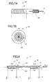
- Figs. 7 are the views for schematically explaining an arrangement of a sensor (iPA sensor) 336 used in the magnetic-field measuring device 10 according to a still further embodiment of the invention.
- Fig. 7(a) is the view for explaining an arrangement of the sensor 336
- Fig. 7(b) is a cross sectional view of the sensor 336 taken in a plane perpendicular to its longitudinal direction. This sensor 336 is used in place of the sensors 36 and 38 used in the embodiment described above.
- the sensor 336 shown in Figs. 7 has substantially the same arrangement as the sensors 36, 38 in the first embodiment. Described more specifically, the sensor 336 has the magnetic material in the form of an amorphous material 346, the electrically conductive body in the form of the conductor wire 42, and the coil 50.
- the amorphous material 346 is an elongate amorphous material having magnetic anisotropy in the form of a wire or a wide strip, for example, which is wound in a coil surrounding the conductor wire 42.
- the wire or strip of the amorphous material 346 may be directly wound on the conductor wire 42, or initially wound so as to define a central cylindrical space, and the conductor wire 42 is then passed through the central cylindrical space.
- the amorphous material 346 and the conductor wire 42 surrounded by the amorphous material 346 may be electrically insulated from each other, as in the preceding third embodiment, or may not be insulated from each other.
- the winding pitch and the number of wound layers of the amorphous material 346 are selected according to the required detection sensitivity of the magnetic-field measuring device 10. Described more specifically, the wire or strip may be wound such that adjacent turns of the wire or strip are not spaced apart from each other, or spaced apart from each other by a predetermined spacing distance. While the wire or strip is required to be wound in at least one layer, it may be wound in a plurality of layers.
- the conductor wire 42 is disposed adjacent to the amorphous material 346, but the longitudinal direction of the conductor wire 42 is not parallel to the direction of length of the wire or strip of the amorphous material 346.
- the coil 50 is a solenoid coil defining an inner space through which the amorphous material 346 and the conductor wire 42 extend.
- the magnetic material is the elongate amorphous material 346 having magnetic anisotropy, and the amorphous material 346 consists of at least one layer wound on the conductor wire 42 so as to surround the conductor wire 42. Accordingly, the magnetic-field measuring device 10 has substantially the same advantages as described above with respect to the first through third embodiments, and can be configured such that the amorphous material 346 and the conductor wire 42 are disposed adjacent to each other.
- Fig. 8 is the view corresponding to that of Fig. 3 , for explaining an arrangement of the probe portion 12 provided in a yet further embodiment of the invention.
- the probe portion 12 according to the present embodiment is used in place of the probe portion 12 of Fig. 3 .
- the two sensors 36 and 38 have the respective amorphous materials 46 and 48 and the respective conductor wires 42 and 44.
- the probe portion 12 of Fig. 8 is different from the probe portion 12 of Fig. 3 in that the two sensors 36 and 38 in the probe portion 12 of Fig. 8 have a common amorphous material 446 and a single conductor wire 442.
- the common amorphous material 446 is commonly used for the two sensors 36 and 38, so as to magnetically connect these two sensors 36 and 38 in series with each other.
- the amorphous material 446 has a symmetrical shape with respect to a straight line of symmetry which passes a midpoint in its direction of easy magnetization, that is, in its longitudinal direction, and which is perpendicular to the direction of easy magnetization.
- the two coils 50 and 52 of the respective sensors 36 and 38 are disposed at respective positions which are symmetrical with each other with respect to the line or plane of symmetry. According to the finding of the present inventors, this arrangement permits symmetry of a magnetic field such as the ambient magnetic field commonly applied to the two sensors 36 and 38, with respect to the longitudinal midpoint or the line of symmetry of the amorphous material 446. Accordingly, where the two sensors 36 and 38 function as a gradiometer, an influence of the ambient magnetic field can be effectively eliminated, so that the two sensors 36 and 38 can improve the accuracy of measurement of the magnetic-field measuring device 10. This improvement is also described in Patent Document 5.
- the present embodiment is configured such that the amorphous material 446 has a symmetrical shape with respect to a straight line of symmetry which passes a midpoint in its direction of easy magnetization, and which is perpendicular to the direction of easy magnetization, and the two coils 50 and 52 of the sensors 36 and 38 are disposed at respective positions which are symmetrical with each other with respect to the line of symmetry, whereby the two sensors 36 and 38 function as a gradiometer. Accordingly, a differential operation performed by the two sensors 36 and 38 permits effective elimination of an influence of the ambient magnetic field such as the terrestrial magnetic field, so that the accuracy of measurement of the magnetic-field measuring device 10 provided with the gradiometer can be improved.
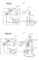
- Fig. 9 is the view for explaining an arrangement of the magnetic-field measuring device 10 according to still another embodiment of the invention.
- a part of the device 10 including the probe portion 12 functions as a sensor probe 212.
- This sensor probe 212 is structurally separated from a main body of the magnetic-field measuring device 10, and the sensor probe 212 and the main body are electrically connected to each other with a cable, so that a magnetic field at a position distant from the main body can be measured.
- the sensor probe 212 includes the pulse generator 22, an AC coupler 224 and an instrumentation amplifier 228, in addition to the probe portion 12.
- the pulse generator 22 is a part of the circuit portion 14.
- the sensor probe 212 is not limited to this arrangement. A part of this sensor probe 212 may be eliminated, or conversely, other parts of the circuit portion 14 may be included in the sensor probe 212.
- the circuit portion 14 in the present embodiment includes the clock portion 20, the power supply portion 21, the pulse generator 22, the AC coupler 224, the instrumentation amplifier 228, an AC coupler 260, a lock-in amplifier 262, and a low-pass filter 264.
- the clock portion 20, power supply portion 21 and pulse generator 22 are identical with those in the first embodiment described above, and will not be described redundantly.
- the clock signal generated by the clock portion 20 is a clock signal having a high degree of accuracy, for example, not lower than a five-digit value.
- the clock portion 20 need not be included in the circuit portion 14, and may be disposed outside the magnetic-field measuring device 10, for example, so that the clock signal is sent from the clock portion 20 to the magnetic-field measuring device 10.
- the outputs of the sensors 36 and 38 are applied to the instrumental amplifier through the AC coupler 224.
- the outputs of the sensors 36 and 38 may be applied to the AC coupler 224 through a band-pass filter which permits passage of only a frequency band from 10kHz to 100MHz, for instance, in order to remove noises from the outputs.
- the outputs of the sensors 36 and 38 are coupled by the AC coupler 224, and a difference between the outputs is obtained by the instrumentation amplifier 228. Further, the difference is amplified by the instrumentation amplifier 228 by a predetermined ratio of amplification.
- the output of the instrumentation amplifier 228 is applied to and coupled by the AC coupler 260.
- a high-pass filter is provided, as needed to remove a high-frequency component of the output of the AC coupler 260 corresponding to the frequency of the clock signal.
- the output of the AC coupler 260 is then applied to the lock-in amplifier 262, which detects an amplitude of a difference between the electromotive forces of the sensors 36 and 38, on the basis of the clock signal generated from the clock portion 20.
- the thus detected amplitude is processed into a continuous value, which is then offset by an amount corresponding to a predetermined offset voltage, and amplified by a predetermined ratio of amplification, for example, by 1000 times.
- the output of the lock-in amplifier 262 is applied to the low-pass filter 264, so that a frequency component lower than a predetermined frequency value is removed from the output, whereby an output of the low-pass filter 264 is obtained.
- This output may represent the offset voltage and a phase of detection (delay time), in addition to the amplified signal value.
- the magnetic-field measuring device 10 has substantially the same advantages as that of the first embodiment.
- the sensor probe 212 is structurally separated from the main body of the magnetic-field measuring device 10, so that the magnetic field at a position distant from the main body can be measured.
- Fig. 10 is the view corresponding to that of Fig. 9 , for explaining an arrangement of the magnetic-field measuring device 10 according to yet another embodiment of the invention.
- the circuit portion 14 in the present embodiment is different from the circuit portion 14 in the preceding embodiments, in that the present circuit portion 14 is provided with a digital processing portion 280.
- This digital processing portion 280 has a function of implementing AD conversion of signals.
- the clock portion 20 is provided in the circuit portion 14 as shown in Fig. 9 .
- a clock portion 282 is provided within the digital processing portion 280, as shown in Fig. 10 .
- a clock signal in the form of a digital signal generated by the clock portion 282 provided within the digital processing portion 280 is converted by a first DA converting portion 283 into an analog signal, which is applied to the pulse generator 22.
- the clock signal may be applied to the pulse generator 22 from a clock portion located outside the magnetic-field measuring device 10, as the sixth embodiment.
- the operations of the AC coupler 224 and the instrumentation amplifier 228 provided to process the outputs of the sensors 36 and 38 are also the same as those in the preceding embodiments, and will not be described redundantly.
- the output of the instrumentation amplifier 228 is applied to an AC coupling portion 270, for a coupling operation.
- a band-pass filter is provided, as needed to pass only components within a predetermined frequency band of the output of the AC coupling portion 270 corresponding to the frequency of the clock signal.
- the output of the AC coupling portion 270 is applied to the digital processing portion 280 wherein a first AD converting portion 284 implements a high-speed AD converting operation to convert the output of the AC coupling portion 270 into a digital signal.
- This first AD converting portion 284 receives the clock signal from the clock portion 282 through the above-described first DA converting portion 283, so that the first AD converting portion 284 operates in synchronization with the clock signal.
- the digital signal generated by the first AD converting portion 284 is processed by a data processing portion 286 described below, and may be stored in a memory device (not shown) provided within the digital processing portion 280, or sent to any other device.
- the data processing portion 286 successive values of the difference between the digital signals obtained by conversion from the output signals of the sensors 36 and 38 are summed to reduce the noise level. Then, the amplitude of the difference at a predetermined phase (at a predetermined point of time delay) is detected. This amplitude corresponds to the magnetic field to be measured.
- the data obtained by the processing operation of the data processing portion 286 are converted by a second DA converting portion 288 into an analog signal, and displayed on a monitor (not shown), for example.
- Fig. 11 is the view indicating a result of an experiment of magnetic-field measurement by the magnetic-field measuring device 10 according to the illustrated embodiments.
- the magnetic-field measuring device shown in Fig. 1 uses the sensors 36 and 38 shown in Fig. 8 .
- the exciting electric current Ie applied from the pulse generator 22 to the conductor wires 42 and 44 of the sensors 36 and 38 is a pulse current of 100mA having a pulse width of 100ns and an amplitude of 5V.
- the conductor wires 42 and 44 are spaced apart from the respective amorphous materials 46 and 48, by a distance of 300 ⁇ m.
- a three-dimensional Helmholtz coil of about two square meters is disposed to apply a weak magnetic field the intensity of which varies in a sine wave, to the sensors 36 and 38 and their vicinities.
- Fig. 11 indicates a chronological variation of the output of one of the sensors 36 and 38 (the output of the sensor 36, for example) of the magnetic-field measuring device 10.
- the magnetic-field measuring device provides the output in the sine wave similar to that of the applied magnetic field.
- the value taken along the vertical line of Fig. 11 represents the output voltage of the sensor (sensor 36, for example).
- the magnetic-field measuring device 10 according to the present embodiment has substantially the same advantages as the magnetic-field measuring device 10 according to the sixth embodiment described above.
- the present magnetic-field measuring device 10 provided with the digital processing portion 280 permits digital processing and storage of data, and an output of digital data.
- the magnetic-field measuring device of the invention is not limited to the magnetic-field measuring device 10 according to the illustrated embodiments wherein the two sensors 36 and 38 are used to provide a gradiometer, and may be modified to implement a magnetic-field measurement by using only one sensor. In this modification, it is not necessary to provide the differential amplifier 28 and the other parts of the circuit portion 14 required to process the outputs of the two sensors.
- the electric current applied from the pulse generator 22 to the conductive portions 42 and 44 of the probe portion 12 takes the form of a rectangular wave.
- the form of the electric current is not limited to the rectangular wave, and may be a sine wave, a sawtooth wave, a triangular wave or an alternating wave, as long as the value of the electric current intermittently changes in a predetermined pattern.
- a direct current component which is offset by a predetermined value in the positive or negative direction with respect to the predetermined pattern may be superimposed on the predetermined pattern.
- the period at which the value of the electric current intermittently changes need not be held constant, and the rectangular wave of the electric current, for example, is not limited to the one in which a high-output time period and a low-output time period are equal to each other.
- the illustrated embodiments use the amorphous materials 46, 48, 146, 246, 346 and 446 in the form of a wire or sheet, as the magnetic materials.
- the magnetic materials are not limited to those amorphous materials, as long as the magnetic materials have magnetic anisotropy. Described more specifically, the magnetic materials may be a liquid having magnetic anisotropy, such as an ion liquid containing particles having magnetic anisotropy, which liquid is accommodated in a suitable container. Further, the magnetic materials may be a composite of the amorphous materials and the above-indicated ion liquid.
- the sample hold circuits 24 and 26 in the circuit portion 14 are configured to detect the peaks (peak values) of the amplitude of the electromotive forces Ecoil1 and Ecoil2 of the respective coils 50 and 52.
- the electromotive forces Ecoil1 and Ecoil2 of the coils 50 and 52 may be initially applied to respective band-pass filters (not shown), for AC coupling operations, so that the outputs of the band-pass filters are applied to the respective sample hold circuits 24 and 26.
- the conductor wires 42 and 44 and the amorphous materials 46 and 48 are electrically insulated from each other in the illustrated embodiments, this electric insulation is not essential. Namely, the conductor wires 42 and 44 may be held in contact with the amorphous materials 46 and 48 such that a very small component of the electric current flowing through each of the conductor wires 42 and 44 leaks into the corresponding amorphous material 46, 48.
- the conductor wires 42 and 44 and the amorphous materials 46 and 48 extend through the inner spaces of the respective solenoid coils 50 and 52.
- this arrangement is not essential. Namely, the amorphous materials 46 and 48 and/or the conductor wires 42 and 44 may be disposed outside the solenoid coils 50 and 52, as long as the electromotive forces are generated on the basis of variations of magnetization of the amorphous materials 46 and 48.
- the cylindrical amorphous material 246 is in the form of a spirally wound sheet.
- the cylindrical amorphous material 246 is not limited to this form. Described more specifically, the cylindrical amorphous material 246 may be formed during its manufacture, by drawing a piece of the original material into a cylindrical or tubular shape.
- the amorphous material 446 commonly used for the two sensors 36 and 38 may be a one-piece body, or at least two pieces of the magnetic material magnetically connected to each other. In the latter case, the at least two pieces need not be held in close contact with each other, and may be spaced apart from each other, as long as the at least two pieces are substantially magnetically connected in series with each other.
- the amorphous material 446 has a symmetrical shape with respect to a straight line of symmetry which is perpendicular to the direction of easy magnetization.
- the amorphous material 446 need not have this symmetrical shape.
- the amorphous material 446 may have a symmetrical shape with respect to a straight plane of symmetry perpendicular to the direction of easy magnetization. That is, the distribution of magnetization of the amorphous material 446 is required to be symmetrical with respect to the midpoint in the direction of easy magnetization.
- the amorphous material 446 is a single amorphous wire.
- the amorphous material 446 need not be the single amorphous wire.
- the single amorphous material (wire) 446 may be replaced by a plurality of wires, as in the illustrated second through fourth embodiments.
- the single amorphous wire or each of the amorphous wires may have a cross sectional shape other than a circular shape.
- the elongate amorphous material 446 may be replaced by a cylindrical amorphous material in the form of a wound sheet, or an elongate amorphous material wound in the form of a solenoid extending through the coils 50 and 52.
- the sensor probe 212 is structurally separated from the main body of the magnetic-field measuring device 10, and the circuit portion 10 has a circuit different from that in the first embodiment.
- this arrangement is not essential.
- the circuit portion 10 may have the same arrangement as that of Fig. 1 , while the sensor probe 212 is structurally separated from the main body of the magnetic-field measuring device 10.
- the circuit portion 14 used in the sixth or seventh embodiment may be used in the first embodiment.
- a difference between the analog output signals of the two sensors 36 and 38 is calculated and amplified by the instrumentation amplifier 228, and the difference is subsequently converted by the first AD converting portion 284 into a digital signal, which is processed by the data processing portion 286.
- this arrangement is not essential.
- the output signals of the sensors 36 and 38 may be amplified by respective amplifiers, and the amplified signals are converted by respective AD converting portions into digital signals, which are applied to the data processing portion 286 so that a difference between the digital signals is calculated by the data processing portion 286.
- the data processing portion 286 may be modified to implement the Fourier transform of chronologically accumulated data, in addition to the processing operation described above. In this case, more accurate calculation can be made on the basis of an amplitude and a surface area of the desired peaks in the frequency domain, and signal variations in the time domain apparently caused by factors other than the variation of the magnetic field can be estimated.
- the induced electromotive forces of the sensors 36 and 38 can be effectively detected by providing the circuit portion 14 with a band-pass filter to adjust the frequency band to be passed, so that the circuit portion 14 is used as an adequate resonance circuit. Namely, not only the peak values of the electromotive forces directly induced during application of the exciting electric current, but also the resonance waveforms during a time period after the application of the exciting electric current can be detected. Accordingly, the sensitivity of detection of the magnetic-field measuring device 10 can be improved by implementing the Fourier transform of the detected resonance waveforms, and adjusting the signal intensity in the desired frequency band in the frequency domain including the resonance waveforms.
- AC couplers 224 and 260 used in the illustrated embodiments may be replaced by DC couplers. This modification has substantially the same advantages as described above.
Landscapes
- Physics & Mathematics (AREA)
- Condensed Matter Physics & Semiconductors (AREA)
- General Physics & Mathematics (AREA)
- Measuring Magnetic Variables (AREA)
Applications Claiming Priority (2)
| Application Number | Priority Date | Filing Date | Title |
|---|---|---|---|
| JP2013046439A JP6281677B2 (ja) | 2013-03-08 | 2013-03-08 | 磁気計測装置 |
| PCT/JP2014/056077 WO2014136975A1 (fr) | 2013-03-08 | 2014-03-07 | Dispositif de mesure de magnétisme |
Publications (3)
| Publication Number | Publication Date |
|---|---|
| EP2975423A1 true EP2975423A1 (fr) | 2016-01-20 |
| EP2975423A4 EP2975423A4 (fr) | 2017-02-22 |
| EP2975423B1 EP2975423B1 (fr) | 2020-02-26 |
Family
ID=51491482
Family Applications (1)
| Application Number | Title | Priority Date | Filing Date |
|---|---|---|---|
| EP14760217.1A Active EP2975423B1 (fr) | 2013-03-08 | 2014-03-07 | Dispositif de mesure de magnétisme |
Country Status (4)
| Country | Link |
|---|---|
| US (1) | US10012705B2 (fr) |
| EP (1) | EP2975423B1 (fr) |
| JP (1) | JP6281677B2 (fr) |
| WO (1) | WO2014136975A1 (fr) |
Cited By (1)
| Publication number | Priority date | Publication date | Assignee | Title |
|---|---|---|---|---|
| RU2658078C1 (ru) * | 2017-05-17 | 2018-06-19 | Федеральное государственное автономное образовательное учреждение высшего образования "Национальный исследовательский Томский политехнический университет" | Способ измерения переменного тока в шине электроустановки |
Families Citing this family (13)
| Publication number | Priority date | Publication date | Assignee | Title |
|---|---|---|---|---|
| JP6422012B2 (ja) * | 2014-02-18 | 2018-11-14 | フジデノロ株式会社 | 磁気検出装置 |
| EP3203585A4 (fr) * | 2014-09-30 | 2018-04-25 | Century Innovation Corporation | Structure de connexion et son procédé de fabrication, ainsi qu'équipement de transport, équipement de courant électrique, équipement de production d'électricité, équipement médical et équipement spatial |
| JP6021238B1 (ja) * | 2015-10-11 | 2016-11-09 | マグネデザイン株式会社 | グラジオセンサ素子およびグラジオセンサ |
| JP6793930B2 (ja) * | 2016-03-31 | 2020-12-02 | 国立大学法人東海国立大学機構 | 磁気センサ、及び、磁気計測装置 |
| DE102016120785A1 (de) * | 2016-11-01 | 2018-05-03 | Krohne Messtechnik Gmbh | Verfahren und Messgerät zur Bestimmung einer Eigenschaft eines Mediums |
| DE102017104994A1 (de) * | 2017-03-09 | 2018-09-13 | Krohne Messtechnik Gmbh | Verfahren zum Betreiben eines induktiven Leitfähigkeitsmessgeräts und diesbezügliches induktives Leitfähigkeitsmessgerät |
| JP7007700B2 (ja) * | 2017-03-30 | 2022-01-25 | 国立大学法人東海国立大学機構 | 磁気計測装置 |
| JP7002739B2 (ja) * | 2017-05-10 | 2022-01-20 | フジデノロ株式会社 | 磁気センサ |
| CN108469593A (zh) * | 2018-04-02 | 2018-08-31 | 南京麦科尼传感技术有限公司 | 一种基于非晶丝正交阵列的高分辨率正交磁通门全方位磁场梯度传感器 |
| JP7326130B2 (ja) * | 2019-11-26 | 2023-08-15 | ローム株式会社 | 磁界検出装置 |
| US11644439B2 (en) * | 2020-01-16 | 2023-05-09 | Shimadzu Corporation | Magnetic body inspection apparatus |
| JP2024013986A (ja) * | 2022-07-21 | 2024-02-01 | 愛知製鋼株式会社 | 磁気検出器 |
| CN117148232B (zh) * | 2023-10-31 | 2024-01-02 | 清华大学 | 一种非晶微丝二维空间磁场检测探头及磁场检测方法 |
Family Cites Families (22)
| Publication number | Priority date | Publication date | Assignee | Title |
|---|---|---|---|---|
| JPS483377U (fr) | 1971-05-25 | 1973-01-16 | ||
| JPS4814275U (fr) * | 1971-06-26 | 1973-02-17 | ||
| US4839624A (en) | 1986-08-01 | 1989-06-13 | Schonstedt Instrument Company | Magnetic cores |
| US4803773A (en) * | 1986-08-01 | 1989-02-14 | Schonstedt Instrument Company | Method of making magnetic cores |
| DE4113490A1 (de) * | 1991-04-25 | 1992-10-29 | Leipzig Lacke Gmbh | Verfahren und vorrichtung zum zerkleinern, dispergieren, benetzen und mischen von pumpfaehigen, unmagnetischen mehrphasengemischen |
| DE59406586D1 (de) * | 1993-03-15 | 1998-09-10 | Siemens Ag | Homogenfeldmagnet mit über Korrekturluftspalte beabstandeten Polplatteneinrichtungen seiner Polschuhe |
| JPH08179020A (ja) * | 1994-12-22 | 1996-07-12 | Sumitomo Metal Mining Co Ltd | 磁気補正回路及びそれを用いた画像表示装置 |
| US5491459A (en) * | 1995-06-23 | 1996-02-13 | The United States Of America As Represented By The Secretary Of The Army | Magic sphere providing distortion-free access to a large internal working space containing a uniform high-intensity magnetic field |
| JP4565072B2 (ja) * | 2001-03-21 | 2010-10-20 | 株式会社産学連携機構九州 | 磁界センサ |
| JP2003004830A (ja) | 2001-06-19 | 2003-01-08 | Aichi Micro Intelligent Corp | 磁界検出装置 |
| JP3801194B2 (ja) | 2003-08-25 | 2006-07-26 | 愛知製鋼株式会社 | 磁気センサ |
| ES2317769B1 (es) * | 2006-12-15 | 2010-02-03 | Micromag 2000, S.L. | Etiqueta magnetoacustica basada en micro-hilo magnetico, y metodo de obtencion de la misma. |
| EP2276082B1 (fr) * | 2008-03-28 | 2016-06-22 | Aichi Steel Corporation | Fil magnéto-sensible, élément à magnéto-impédance et capteur à magnéto-impédance |
| US20110163744A1 (en) * | 2008-04-21 | 2011-07-07 | National University Corporation Nagoya University | Cellular tissue magnetic signal detecting apparatus |
| JP4655247B2 (ja) | 2009-04-23 | 2011-03-23 | 愛知製鋼株式会社 | 超高感度マグネトインピーダンスセンサ |
| JP2011053160A (ja) * | 2009-09-04 | 2011-03-17 | Hioki Ee Corp | 磁気検出センサ |
| EP2544042B1 (fr) * | 2010-03-02 | 2016-08-31 | National Institute for Materials Science | Résonateur à ondes électromagnétiques, son procédé de fabrication et élément de générateur à ondes électromagnétiques l'employant |
| JP5429717B2 (ja) | 2011-03-07 | 2014-02-26 | 国立大学法人名古屋大学 | 磁気検出装置 |
| JP2012198038A (ja) * | 2011-03-18 | 2012-10-18 | Yokogawa Electric Corp | 磁性体部材とその製造方法 |
| US8803519B2 (en) * | 2011-07-29 | 2014-08-12 | Seagate Technology Llc | Enhanced magnetic sensor biasing yoke |
| JP5673951B2 (ja) * | 2011-08-23 | 2015-02-18 | 独立行政法人産業技術総合研究所 | 電界強磁性共鳴励起方法及びそれを用いた磁気機能素子 |
| US9406320B2 (en) * | 2014-08-20 | 2016-08-02 | HGST Netherlands B.V. | Scissor unidirectional biasing with hard bias stabilized soft bias |
-
2013
- 2013-03-08 JP JP2013046439A patent/JP6281677B2/ja active Active
-
2014
- 2014-03-07 WO PCT/JP2014/056077 patent/WO2014136975A1/fr active Application Filing
- 2014-03-07 EP EP14760217.1A patent/EP2975423B1/fr active Active
- 2014-03-07 US US14/773,633 patent/US10012705B2/en active Active
Non-Patent Citations (1)
| Title |
|---|
| See references of WO2014136975A1 * |
Cited By (1)
| Publication number | Priority date | Publication date | Assignee | Title |
|---|---|---|---|---|
| RU2658078C1 (ru) * | 2017-05-17 | 2018-06-19 | Федеральное государственное автономное образовательное учреждение высшего образования "Национальный исследовательский Томский политехнический университет" | Способ измерения переменного тока в шине электроустановки |
Also Published As
| Publication number | Publication date |
|---|---|
| JP6281677B2 (ja) | 2018-02-21 |
| JP2014173980A (ja) | 2014-09-22 |
| EP2975423B1 (fr) | 2020-02-26 |
| US20160041236A1 (en) | 2016-02-11 |
| US10012705B2 (en) | 2018-07-03 |
| WO2014136975A1 (fr) | 2014-09-12 |
| EP2975423A4 (fr) | 2017-02-22 |
Similar Documents
| Publication | Publication Date | Title |
|---|---|---|
| US10012705B2 (en) | Magnetism measurement device | |
| US9759785B2 (en) | Magnetic-field detecting device | |
| Silva et al. | High sensitivity giant magnetoimpedance (GMI) magnetic transducer: magnitude versus phase sensing | |
| US20030016010A1 (en) | Apparatus for measuring a magnetic field | |
| JP2018146314A (ja) | 磁気センサ、磁気センサ装置 | |
| CN104849679A (zh) | 磁探头和包括该磁探头的磁场传感器 | |
| US7196514B2 (en) | Multi-conductive ferromagnetic core, variable permeability field sensor and method | |
| JP2020521979A (ja) | トンネル磁気抵抗を有する磁気抵抗センサの低周波雑音を抑制するためのシステムおよび方法 | |
| JP2014190774A (ja) | 磁気計測装置 | |
| US20130207651A1 (en) | Fluxgate sensor | |
| US20200256930A1 (en) | Current-sensing method of gmi magnetic field measurement | |
| US11726149B2 (en) | Magnetic sensor and inspection device | |
| US11513173B2 (en) | Magnetic sensor and inspection device | |
| US6853186B2 (en) | Variable permeability magnetic field sensor and method | |
| Breth et al. | Fluxgate principle applied to a magnetic tunnel junction for weak magnetic field sensing | |
| JP7482046B2 (ja) | 磁気センサ及び検査装置 | |
| Vyhnanek et al. | Experimental comparison of the low-frequency noise of small-size magnetic sensors | |
| Suhaimi et al. | Development of a compact and sensitive AC magnetometer for evaluation of magnetic nanoparticles solution | |
| Doan et al. | Magnetization measurement system with giant magnetoresistance zero-field detector | |
| JP7007700B2 (ja) | 磁気計測装置 | |
| Baglio et al. | Conception of a Temperature Sensor Based on 100-μm CoFeSiB Ferromagnetic Wire | |
| Kollu et al. | Prototype Milli Gauss Meter Using Giant Magnetoimpedance Effect in Self Biased Amorphous Ribbon | |
| Dhani et al. | Characterization of AC current sensor based on giant magnetoresistance and coil for power meter design | |
| Novkovski | Progress and limitations in magnetic field measurements | |
| Semirov et al. | Influence of thermo-stress factor on magnetoimpedance of soft magnetic materials |
Legal Events
| Date | Code | Title | Description |
|---|---|---|---|
| PUAI | Public reference made under article 153(3) epc to a published international application that has entered the european phase |
Free format text: ORIGINAL CODE: 0009012 |
|
| 17P | Request for examination filed |
Effective date: 20151007 |
|
| AK | Designated contracting states |
Kind code of ref document: A1 Designated state(s): AL AT BE BG CH CY CZ DE DK EE ES FI FR GB GR HR HU IE IS IT LI LT LU LV MC MK MT NL NO PL PT RO RS SE SI SK SM TR |
|
| AX | Request for extension of the european patent |
Extension state: BA ME |
|
| DAX | Request for extension of the european patent (deleted) | ||
| A4 | Supplementary search report drawn up and despatched |
Effective date: 20170125 |
|
| RIC1 | Information provided on ipc code assigned before grant |
Ipc: G01R 33/02 20060101AFI20170119BHEP |
|
| GRAP | Despatch of communication of intention to grant a patent |
Free format text: ORIGINAL CODE: EPIDOSNIGR1 |
|
| STAA | Information on the status of an ep patent application or granted ep patent |
Free format text: STATUS: GRANT OF PATENT IS INTENDED |
|
| INTG | Intention to grant announced |
Effective date: 20190910 |
|
| GRAS | Grant fee paid |
Free format text: ORIGINAL CODE: EPIDOSNIGR3 |
|
| GRAA | (expected) grant |
Free format text: ORIGINAL CODE: 0009210 |
|
| STAA | Information on the status of an ep patent application or granted ep patent |
Free format text: STATUS: THE PATENT HAS BEEN GRANTED |
|
| RIN1 | Information on inventor provided before grant (corrected) |
Inventor name: NAKAYAMA SHINSUKE Inventor name: MIYAZAKI HIDEKI |
|
| AK | Designated contracting states |
Kind code of ref document: B1 Designated state(s): AL AT BE BG CH CY CZ DE DK EE ES FI FR GB GR HR HU IE IS IT LI LT LU LV MC MK MT NL NO PL PT RO RS SE SI SK SM TR |
|
| REG | Reference to a national code |
Ref country code: GB Ref legal event code: FG4D |
|
| REG | Reference to a national code |
Ref country code: CH Ref legal event code: EP |
|
| REG | Reference to a national code |
Ref country code: AT Ref legal event code: REF Ref document number: 1238303 Country of ref document: AT Kind code of ref document: T Effective date: 20200315 |
|
| REG | Reference to a national code |
Ref country code: IE Ref legal event code: FG4D |
|
| REG | Reference to a national code |
Ref country code: DE Ref legal event code: R096 Ref document number: 602014061534 Country of ref document: DE |
|
| PG25 | Lapsed in a contracting state [announced via postgrant information from national office to epo] |
Ref country code: NO Free format text: LAPSE BECAUSE OF FAILURE TO SUBMIT A TRANSLATION OF THE DESCRIPTION OR TO PAY THE FEE WITHIN THE PRESCRIBED TIME-LIMIT Effective date: 20200526 Ref country code: RS Free format text: LAPSE BECAUSE OF FAILURE TO SUBMIT A TRANSLATION OF THE DESCRIPTION OR TO PAY THE FEE WITHIN THE PRESCRIBED TIME-LIMIT Effective date: 20200226 Ref country code: FI Free format text: LAPSE BECAUSE OF FAILURE TO SUBMIT A TRANSLATION OF THE DESCRIPTION OR TO PAY THE FEE WITHIN THE PRESCRIBED TIME-LIMIT Effective date: 20200226 |
|
| REG | Reference to a national code |
Ref country code: NL Ref legal event code: MP Effective date: 20200226 |
|
| REG | Reference to a national code |
Ref country code: LT Ref legal event code: MG4D |
|
| PG25 | Lapsed in a contracting state [announced via postgrant information from national office to epo] |
Ref country code: GR Free format text: LAPSE BECAUSE OF FAILURE TO SUBMIT A TRANSLATION OF THE DESCRIPTION OR TO PAY THE FEE WITHIN THE PRESCRIBED TIME-LIMIT Effective date: 20200527 Ref country code: HR Free format text: LAPSE BECAUSE OF FAILURE TO SUBMIT A TRANSLATION OF THE DESCRIPTION OR TO PAY THE FEE WITHIN THE PRESCRIBED TIME-LIMIT Effective date: 20200226 Ref country code: BG Free format text: LAPSE BECAUSE OF FAILURE TO SUBMIT A TRANSLATION OF THE DESCRIPTION OR TO PAY THE FEE WITHIN THE PRESCRIBED TIME-LIMIT Effective date: 20200526 Ref country code: LV Free format text: LAPSE BECAUSE OF FAILURE TO SUBMIT A TRANSLATION OF THE DESCRIPTION OR TO PAY THE FEE WITHIN THE PRESCRIBED TIME-LIMIT Effective date: 20200226 Ref country code: SE Free format text: LAPSE BECAUSE OF FAILURE TO SUBMIT A TRANSLATION OF THE DESCRIPTION OR TO PAY THE FEE WITHIN THE PRESCRIBED TIME-LIMIT Effective date: 20200226 Ref country code: IS Free format text: LAPSE BECAUSE OF FAILURE TO SUBMIT A TRANSLATION OF THE DESCRIPTION OR TO PAY THE FEE WITHIN THE PRESCRIBED TIME-LIMIT Effective date: 20200626 |
|
| PG25 | Lapsed in a contracting state [announced via postgrant information from national office to epo] |
Ref country code: NL Free format text: LAPSE BECAUSE OF FAILURE TO SUBMIT A TRANSLATION OF THE DESCRIPTION OR TO PAY THE FEE WITHIN THE PRESCRIBED TIME-LIMIT Effective date: 20200226 |
|
| PG25 | Lapsed in a contracting state [announced via postgrant information from national office to epo] |
Ref country code: RO Free format text: LAPSE BECAUSE OF FAILURE TO SUBMIT A TRANSLATION OF THE DESCRIPTION OR TO PAY THE FEE WITHIN THE PRESCRIBED TIME-LIMIT Effective date: 20200226 Ref country code: CZ Free format text: LAPSE BECAUSE OF FAILURE TO SUBMIT A TRANSLATION OF THE DESCRIPTION OR TO PAY THE FEE WITHIN THE PRESCRIBED TIME-LIMIT Effective date: 20200226 Ref country code: ES Free format text: LAPSE BECAUSE OF FAILURE TO SUBMIT A TRANSLATION OF THE DESCRIPTION OR TO PAY THE FEE WITHIN THE PRESCRIBED TIME-LIMIT Effective date: 20200226 Ref country code: SK Free format text: LAPSE BECAUSE OF FAILURE TO SUBMIT A TRANSLATION OF THE DESCRIPTION OR TO PAY THE FEE WITHIN THE PRESCRIBED TIME-LIMIT Effective date: 20200226 Ref country code: DK Free format text: LAPSE BECAUSE OF FAILURE TO SUBMIT A TRANSLATION OF THE DESCRIPTION OR TO PAY THE FEE WITHIN THE PRESCRIBED TIME-LIMIT Effective date: 20200226 Ref country code: PT Free format text: LAPSE BECAUSE OF FAILURE TO SUBMIT A TRANSLATION OF THE DESCRIPTION OR TO PAY THE FEE WITHIN THE PRESCRIBED TIME-LIMIT Effective date: 20200719 Ref country code: LT Free format text: LAPSE BECAUSE OF FAILURE TO SUBMIT A TRANSLATION OF THE DESCRIPTION OR TO PAY THE FEE WITHIN THE PRESCRIBED TIME-LIMIT Effective date: 20200226 Ref country code: SM Free format text: LAPSE BECAUSE OF FAILURE TO SUBMIT A TRANSLATION OF THE DESCRIPTION OR TO PAY THE FEE WITHIN THE PRESCRIBED TIME-LIMIT Effective date: 20200226 Ref country code: EE Free format text: LAPSE BECAUSE OF FAILURE TO SUBMIT A TRANSLATION OF THE DESCRIPTION OR TO PAY THE FEE WITHIN THE PRESCRIBED TIME-LIMIT Effective date: 20200226 |
|
| REG | Reference to a national code |
Ref country code: CH Ref legal event code: PL |
|
| REG | Reference to a national code |
Ref country code: AT Ref legal event code: MK05 Ref document number: 1238303 Country of ref document: AT Kind code of ref document: T Effective date: 20200226 |
|
| REG | Reference to a national code |
Ref country code: DE Ref legal event code: R097 Ref document number: 602014061534 Country of ref document: DE |
|
| PG25 | Lapsed in a contracting state [announced via postgrant information from national office to epo] |
Ref country code: MC Free format text: LAPSE BECAUSE OF FAILURE TO SUBMIT A TRANSLATION OF THE DESCRIPTION OR TO PAY THE FEE WITHIN THE PRESCRIBED TIME-LIMIT Effective date: 20200226 |
|
| REG | Reference to a national code |
Ref country code: BE Ref legal event code: MM Effective date: 20200331 |
|
| PG25 | Lapsed in a contracting state [announced via postgrant information from national office to epo] |
Ref country code: LU Free format text: LAPSE BECAUSE OF NON-PAYMENT OF DUE FEES Effective date: 20200307 |
|
| PLBE | No opposition filed within time limit |
Free format text: ORIGINAL CODE: 0009261 |
|
| STAA | Information on the status of an ep patent application or granted ep patent |
Free format text: STATUS: NO OPPOSITION FILED WITHIN TIME LIMIT |
|
| PG25 | Lapsed in a contracting state [announced via postgrant information from national office to epo] |
Ref country code: IT Free format text: LAPSE BECAUSE OF FAILURE TO SUBMIT A TRANSLATION OF THE DESCRIPTION OR TO PAY THE FEE WITHIN THE PRESCRIBED TIME-LIMIT Effective date: 20200226 Ref country code: LI Free format text: LAPSE BECAUSE OF NON-PAYMENT OF DUE FEES Effective date: 20200331 Ref country code: AT Free format text: LAPSE BECAUSE OF FAILURE TO SUBMIT A TRANSLATION OF THE DESCRIPTION OR TO PAY THE FEE WITHIN THE PRESCRIBED TIME-LIMIT Effective date: 20200226 Ref country code: IE Free format text: LAPSE BECAUSE OF NON-PAYMENT OF DUE FEES Effective date: 20200307 Ref country code: CH Free format text: LAPSE BECAUSE OF NON-PAYMENT OF DUE FEES Effective date: 20200331 |
|
| 26N | No opposition filed |
Effective date: 20201127 |
|
| PG25 | Lapsed in a contracting state [announced via postgrant information from national office to epo] |
Ref country code: PL Free format text: LAPSE BECAUSE OF FAILURE TO SUBMIT A TRANSLATION OF THE DESCRIPTION OR TO PAY THE FEE WITHIN THE PRESCRIBED TIME-LIMIT Effective date: 20200226 Ref country code: SI Free format text: LAPSE BECAUSE OF FAILURE TO SUBMIT A TRANSLATION OF THE DESCRIPTION OR TO PAY THE FEE WITHIN THE PRESCRIBED TIME-LIMIT Effective date: 20200226 Ref country code: BE Free format text: LAPSE BECAUSE OF NON-PAYMENT OF DUE FEES Effective date: 20200331 |
|
| PG25 | Lapsed in a contracting state [announced via postgrant information from national office to epo] |
Ref country code: TR Free format text: LAPSE BECAUSE OF FAILURE TO SUBMIT A TRANSLATION OF THE DESCRIPTION OR TO PAY THE FEE WITHIN THE PRESCRIBED TIME-LIMIT Effective date: 20200226 Ref country code: MT Free format text: LAPSE BECAUSE OF FAILURE TO SUBMIT A TRANSLATION OF THE DESCRIPTION OR TO PAY THE FEE WITHIN THE PRESCRIBED TIME-LIMIT Effective date: 20200226 Ref country code: CY Free format text: LAPSE BECAUSE OF FAILURE TO SUBMIT A TRANSLATION OF THE DESCRIPTION OR TO PAY THE FEE WITHIN THE PRESCRIBED TIME-LIMIT Effective date: 20200226 |
|
| PG25 | Lapsed in a contracting state [announced via postgrant information from national office to epo] |
Ref country code: MK Free format text: LAPSE BECAUSE OF FAILURE TO SUBMIT A TRANSLATION OF THE DESCRIPTION OR TO PAY THE FEE WITHIN THE PRESCRIBED TIME-LIMIT Effective date: 20200226 Ref country code: AL Free format text: LAPSE BECAUSE OF FAILURE TO SUBMIT A TRANSLATION OF THE DESCRIPTION OR TO PAY THE FEE WITHIN THE PRESCRIBED TIME-LIMIT Effective date: 20200226 |
|
| PGFP | Annual fee paid to national office [announced via postgrant information from national office to epo] |
Ref country code: FR Payment date: 20230215 Year of fee payment: 10 |
|
| PGFP | Annual fee paid to national office [announced via postgrant information from national office to epo] |
Ref country code: DE Payment date: 20240305 Year of fee payment: 11 Ref country code: GB Payment date: 20240318 Year of fee payment: 11 |