EP2974015B1 - Circuit and method to extend a signal comparison voltage range - Google Patents
Circuit and method to extend a signal comparison voltage range Download PDFInfo
- Publication number
- EP2974015B1 EP2974015B1 EP14713717.8A EP14713717A EP2974015B1 EP 2974015 B1 EP2974015 B1 EP 2974015B1 EP 14713717 A EP14713717 A EP 14713717A EP 2974015 B1 EP2974015 B1 EP 2974015B1
- Authority
- EP
- European Patent Office
- Prior art keywords
- coupled
- voltage
- circuit
- dynamic
- transistor
- Prior art date
- Legal status (The legal status is an assumption and is not a legal conclusion. Google has not performed a legal analysis and makes no representation as to the accuracy of the status listed.)
- Not-in-force
Links
Images

Classifications
-
- H—ELECTRICITY
- H03—ELECTRONIC CIRCUITRY
- H03K—PULSE TECHNIQUE
- H03K3/00—Circuits for generating electric pulses; Monostable, bistable or multistable circuits
- H03K3/02—Generators characterised by the type of circuit or by the means used for producing pulses
- H03K3/353—Generators characterised by the type of circuit or by the means used for producing pulses by the use, as active elements, of field-effect transistors with internal or external positive feedback
- H03K3/356—Bistable circuits
- H03K3/356104—Bistable circuits using complementary field-effect transistors
- H03K3/356113—Bistable circuits using complementary field-effect transistors using additional transistors in the input circuit
- H03K3/35613—Bistable circuits using complementary field-effect transistors using additional transistors in the input circuit the input circuit having a differential configuration
-
- H—ELECTRICITY
- H03—ELECTRONIC CIRCUITRY
- H03K—PULSE TECHNIQUE
- H03K5/00—Manipulating of pulses not covered by one of the other main groups of this subclass
-
- H—ELECTRICITY
- H03—ELECTRONIC CIRCUITRY
- H03K—PULSE TECHNIQUE
- H03K19/00—Logic circuits, i.e. having at least two inputs acting on one output; Inverting circuits
- H03K19/0008—Arrangements for reducing power consumption
- H03K19/0016—Arrangements for reducing power consumption by using a control or a clock signal, e.g. in order to apply power supply
-
- H—ELECTRICITY
- H03—ELECTRONIC CIRCUITRY
- H03K—PULSE TECHNIQUE
- H03K3/00—Circuits for generating electric pulses; Monostable, bistable or multistable circuits
- H03K3/01—Details
- H03K3/012—Modifications of generator to improve response time or to decrease power consumption
-
- H—ELECTRICITY
- H03—ELECTRONIC CIRCUITRY
- H03K—PULSE TECHNIQUE
- H03K3/00—Circuits for generating electric pulses; Monostable, bistable or multistable circuits
- H03K3/02—Generators characterised by the type of circuit or by the means used for producing pulses
- H03K3/353—Generators characterised by the type of circuit or by the means used for producing pulses by the use, as active elements, of field-effect transistors with internal or external positive feedback
- H03K3/356—Bistable circuits
- H03K3/356104—Bistable circuits using complementary field-effect transistors
- H03K3/356113—Bistable circuits using complementary field-effect transistors using additional transistors in the input circuit
- H03K3/35613—Bistable circuits using complementary field-effect transistors using additional transistors in the input circuit the input circuit having a differential configuration
- H03K3/356139—Bistable circuits using complementary field-effect transistors using additional transistors in the input circuit the input circuit having a differential configuration with synchronous operation
-
- H—ELECTRICITY
- H03—ELECTRONIC CIRCUITRY
- H03K—PULSE TECHNIQUE
- H03K5/00—Manipulating of pulses not covered by one of the other main groups of this subclass
- H03K5/22—Circuits having more than one input and one output for comparing pulses or pulse trains with each other according to input signal characteristics, e.g. slope, integral
- H03K5/24—Circuits having more than one input and one output for comparing pulses or pulse trains with each other according to input signal characteristics, e.g. slope, integral the characteristic being amplitude
- H03K5/2472—Circuits having more than one input and one output for comparing pulses or pulse trains with each other according to input signal characteristics, e.g. slope, integral the characteristic being amplitude using field effect transistors
- H03K5/2481—Circuits having more than one input and one output for comparing pulses or pulse trains with each other according to input signal characteristics, e.g. slope, integral the characteristic being amplitude using field effect transistors with at least one differential stage
-
- H—ELECTRICITY
- H03—ELECTRONIC CIRCUITRY
- H03K—PULSE TECHNIQUE
- H03K5/00—Manipulating of pulses not covered by one of the other main groups of this subclass
- H03K5/22—Circuits having more than one input and one output for comparing pulses or pulse trains with each other according to input signal characteristics, e.g. slope, integral
- H03K5/24—Circuits having more than one input and one output for comparing pulses or pulse trains with each other according to input signal characteristics, e.g. slope, integral the characteristic being amplitude
- H03K5/2472—Circuits having more than one input and one output for comparing pulses or pulse trains with each other according to input signal characteristics, e.g. slope, integral the characteristic being amplitude using field effect transistors
- H03K5/249—Circuits having more than one input and one output for comparing pulses or pulse trains with each other according to input signal characteristics, e.g. slope, integral the characteristic being amplitude using field effect transistors using clock signals
Definitions
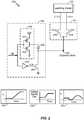
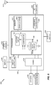
- extending the voltage range of the comparator 104 by biasing the voltage level of the dynamic node 108 (i.e., biasing the voltage level of the source of the second transistor 210) and maintaining the voltage level of the second input signal (Vin-) may increase the gate-to-source voltage of the second transistor 210 to a level that is greater than the threshold voltage of the second transistor 210.
- the first and second transistors 208, 210 may be activated to discharge the first and second pre-charged nodes 212, 214, respectively.
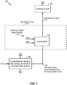
- the circuit 200 of FIG. 3 may extend a voltage range of the comparator 104 to activate the first and second transistors 208, 210.
- the clocked circuit 106 may selectively bias the dynamic node 108 to a negative voltage (i.e., a voltage less than ground) to increase the gate-to-source voltage of the first and second transistors 208, 210 to a voltage level greater than a threshold voltage of the first and second transistors 208, 210.
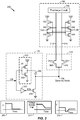
- the first inverter 432, 452 of the pair of cross-coupled inverters toggles and outputs a low voltage signal at the first output (Out) of the latching circuit 402.
- the low voltage signal at the first output (Out) drives the second inverter 434, 454 of the pair of cross-coupled inverters to maintain a high voltage signal at the second output (OutB) of the latching circuit 402.
- the low voltage signal at the first output (Out) may be applied to the gate of the sixth PMOS transistor 454 and to the gate of the fourth NMOS transistor 434.
- the method 500 of FIG. 5 may extend a signal comparison voltage range of the comparator 104 to activate the first and second transistors 208, 210.
- the clocked circuit 106 may selectively bias the dynamic node 108 to a negative voltage (i.e., a voltage less than ground) to increase the gate-to-source voltage of the first and second transistors 208, 210 to a voltage level greater than a threshold voltage of the first and second transistors 208, 210.
- Increasing the gate-to-source voltage of the first and second transistors 208, 210 may enable the transistors 208, 210 to activate (or operate in a saturation region of operation) without increasing a voltage supply (Vdd) of the comparator 104.
Landscapes
- Physics & Mathematics (AREA)
- Nonlinear Science (AREA)
- Engineering & Computer Science (AREA)
- Computer Hardware Design (AREA)
- Computing Systems (AREA)
- General Engineering & Computer Science (AREA)
- Mathematical Physics (AREA)
- Manipulation Of Pulses (AREA)
- Logic Circuits (AREA)
Applications Claiming Priority (2)
| Application Number | Priority Date | Filing Date | Title |
|---|---|---|---|
| US13/797,645 US9356586B2 (en) | 2013-03-12 | 2013-03-12 | Circuit and method to extend a signal comparison voltage range |
| PCT/US2014/021835 WO2014164311A1 (en) | 2013-03-12 | 2014-03-07 | Circuit and method to extend a signal comparison voltage range |
Publications (2)
| Publication Number | Publication Date |
|---|---|
| EP2974015A1 EP2974015A1 (en) | 2016-01-20 |
| EP2974015B1 true EP2974015B1 (en) | 2020-09-02 |
Family
ID=50390275
Family Applications (1)
| Application Number | Title | Priority Date | Filing Date |
|---|---|---|---|
| EP14713717.8A Not-in-force EP2974015B1 (en) | 2013-03-12 | 2014-03-07 | Circuit and method to extend a signal comparison voltage range |
Country Status (6)
| Country | Link |
|---|---|
| US (2) | US9356586B2 (enExample) |
| EP (1) | EP2974015B1 (enExample) |
| JP (1) | JP2016510201A (enExample) |
| KR (1) | KR20150127627A (enExample) |
| CN (1) | CN105009451B (enExample) |
| WO (1) | WO2014164311A1 (enExample) |
Families Citing this family (7)
| Publication number | Priority date | Publication date | Assignee | Title |
|---|---|---|---|---|
| US9356586B2 (en) | 2013-03-12 | 2016-05-31 | Qualcomm Incorporated | Circuit and method to extend a signal comparison voltage range |
| US11115022B2 (en) * | 2015-05-07 | 2021-09-07 | Northwestern University | System and method for integrated circuit usage tracking circuit with fast tracking time for hardware security and re-configurability |
| US10181861B1 (en) * | 2017-12-29 | 2019-01-15 | Texas Instruments Incorporated | Reference voltage control circuit for a two-step flash analog-to-digital converter |
| CN108345565B (zh) * | 2018-01-22 | 2023-05-23 | 京微齐力(北京)科技有限公司 | 一种控制外接电源输出的可编程电路及其方法 |
| US10355693B1 (en) * | 2018-03-14 | 2019-07-16 | Qualcomm Incorporated | Extended GPIO (eGPIO) |
| US10969416B2 (en) * | 2018-12-13 | 2021-04-06 | Silicon Laboratories Inc. | System and method of duplicate circuit block swapping for noise reduction |
| KR102714233B1 (ko) * | 2019-04-05 | 2024-10-08 | 에스케이하이닉스 시스템아이씨 (우시) 씨오엘티디 | 불휘발성 메모리 장치의 동적 전압 공급 회로 및 이를 포함하는 불휘발성 메모리 장치 |
Citations (1)
| Publication number | Priority date | Publication date | Assignee | Title |
|---|---|---|---|---|
| JP2012227588A (ja) * | 2011-04-15 | 2012-11-15 | Fujitsu Semiconductor Ltd | 比較回路及びアナログデジタル変換回路 |
Family Cites Families (13)
| Publication number | Priority date | Publication date | Assignee | Title |
|---|---|---|---|---|
| US4047059A (en) * | 1976-05-24 | 1977-09-06 | Rca Corporation | Comparator circuit |
| US5583457A (en) | 1992-04-14 | 1996-12-10 | Hitachi, Ltd. | Semiconductor integrated circuit device having power reduction mechanism |
| JP3561012B2 (ja) * | 1994-11-07 | 2004-09-02 | 株式会社ルネサステクノロジ | 半導体集積回路装置 |
| US6181165B1 (en) * | 1998-03-09 | 2001-01-30 | Siemens Aktiengesellschaft | Reduced voltage input/reduced voltage output tri-state buffers |
| US6353342B1 (en) * | 2000-10-30 | 2002-03-05 | Intel Corporation | Integrated circuit bus architecture including a full-swing, clocked, common-gate receiver for fast on-chip signal transmission |
| JP3874247B2 (ja) | 2001-12-25 | 2007-01-31 | 株式会社ルネサステクノロジ | 半導体集積回路装置 |
| US6593801B1 (en) | 2002-06-07 | 2003-07-15 | Pericom Semiconductor Corp. | Power down mode signaled by differential transmitter's high-Z state detected by receiver sensing same voltage on differential lines |
| US20040263213A1 (en) * | 2003-06-26 | 2004-12-30 | Oliver Kiehl | Current source |
| US7138825B2 (en) | 2004-06-29 | 2006-11-21 | International Business Machines Corporation | Charge recycling power gate |
| US8030999B2 (en) | 2004-09-20 | 2011-10-04 | The Trustees Of Columbia University In The City Of New York | Low voltage operational transconductance amplifier circuits |
| US7221190B2 (en) | 2005-03-14 | 2007-05-22 | Texas Instruments Incorporated | Differential comparator with extended common mode voltage range |
| TWI470939B (zh) * | 2009-11-04 | 2015-01-21 | Pixart Imaging Inc | 類比至數位轉換器及其相關之校準比較器 |
| US9356586B2 (en) * | 2013-03-12 | 2016-05-31 | Qualcomm Incorporated | Circuit and method to extend a signal comparison voltage range |
-
2013
- 2013-03-12 US US13/797,645 patent/US9356586B2/en not_active Expired - Fee Related
-
2014
- 2014-03-07 KR KR1020157026136A patent/KR20150127627A/ko not_active Withdrawn
- 2014-03-07 CN CN201480012397.4A patent/CN105009451B/zh not_active Expired - Fee Related
- 2014-03-07 EP EP14713717.8A patent/EP2974015B1/en not_active Not-in-force
- 2014-03-07 WO PCT/US2014/021835 patent/WO2014164311A1/en not_active Ceased
- 2014-03-07 JP JP2016500858A patent/JP2016510201A/ja active Pending
-
2016
- 2016-05-03 US US15/144,929 patent/US9722585B2/en not_active Expired - Fee Related
Patent Citations (1)
| Publication number | Priority date | Publication date | Assignee | Title |
|---|---|---|---|---|
| JP2012227588A (ja) * | 2011-04-15 | 2012-11-15 | Fujitsu Semiconductor Ltd | 比較回路及びアナログデジタル変換回路 |
Also Published As
| Publication number | Publication date |
|---|---|
| WO2014164311A1 (en) | 2014-10-09 |
| CN105009451B (zh) | 2017-10-24 |
| KR20150127627A (ko) | 2015-11-17 |
| US20140266307A1 (en) | 2014-09-18 |
| EP2974015A1 (en) | 2016-01-20 |
| JP2016510201A (ja) | 2016-04-04 |
| US20160248407A1 (en) | 2016-08-25 |
| CN105009451A (zh) | 2015-10-28 |
| US9356586B2 (en) | 2016-05-31 |
| US9722585B2 (en) | 2017-08-01 |
Similar Documents
| Publication | Publication Date | Title |
|---|---|---|
| EP2974015B1 (en) | Circuit and method to extend a signal comparison voltage range | |
| US9124276B2 (en) | Sense amplifier including a level shifter | |
| US7884645B2 (en) | Voltage level shifting circuit and method | |
| US20100176892A1 (en) | Ultra Low Power Oscillator | |
| US9680472B2 (en) | Voltage level shifter circuit | |
| CN103814366B (zh) | 用于减小交叉耦合效应的系统和方法 | |
| US8054122B2 (en) | Analog switch with a low flatness operating characteristic | |
| KR20090123004A (ko) | 전압 스윙을 제어하는 회로 장치 및 방법 | |
| US10133285B2 (en) | Voltage droop control | |
| US20060164134A1 (en) | Buffer circuit and integrated circuit | |
| EP3008820B1 (en) | Self-biased receiver | |
| US7557630B2 (en) | Sense amplifier-based flip-flop for reducing output delay time and method thereof | |
| JP2006311176A (ja) | クロック検出回路ならびにそれを用いた信号処理回路、情報端末装置 |
Legal Events
| Date | Code | Title | Description |
|---|---|---|---|
| PUAI | Public reference made under article 153(3) epc to a published international application that has entered the european phase |
Free format text: ORIGINAL CODE: 0009012 |
|
| 17P | Request for examination filed |
Effective date: 20150806 |
|
| AK | Designated contracting states |
Kind code of ref document: A1 Designated state(s): AL AT BE BG CH CY CZ DE DK EE ES FI FR GB GR HR HU IE IS IT LI LT LU LV MC MK MT NL NO PL PT RO RS SE SI SK SM TR |
|
| AX | Request for extension of the european patent |
Extension state: BA ME |
|
| DAX | Request for extension of the european patent (deleted) | ||
| STAA | Information on the status of an ep patent application or granted ep patent |
Free format text: STATUS: EXAMINATION IS IN PROGRESS |
|
| 17Q | First examination report despatched |
Effective date: 20180315 |
|
| GRAP | Despatch of communication of intention to grant a patent |
Free format text: ORIGINAL CODE: EPIDOSNIGR1 |
|
| RIC1 | Information provided on ipc code assigned before grant |
Ipc: H03K 5/00 20060101ALI20200217BHEP Ipc: H03K 3/356 20060101ALI20200217BHEP Ipc: H03K 19/00 20060101ALI20200217BHEP Ipc: H03K 5/24 20060101ALI20200217BHEP Ipc: H03K 3/012 20060101AFI20200217BHEP |
|
| STAA | Information on the status of an ep patent application or granted ep patent |
Free format text: STATUS: GRANT OF PATENT IS INTENDED |
|
| INTG | Intention to grant announced |
Effective date: 20200326 |
|
| GRAS | Grant fee paid |
Free format text: ORIGINAL CODE: EPIDOSNIGR3 |
|
| GRAA | (expected) grant |
Free format text: ORIGINAL CODE: 0009210 |
|
| STAA | Information on the status of an ep patent application or granted ep patent |
Free format text: STATUS: THE PATENT HAS BEEN GRANTED |
|
| AK | Designated contracting states |
Kind code of ref document: B1 Designated state(s): AL AT BE BG CH CY CZ DE DK EE ES FI FR GB GR HR HU IE IS IT LI LT LU LV MC MK MT NL NO PL PT RO RS SE SI SK SM TR |
|
| REG | Reference to a national code |
Ref country code: GB Ref legal event code: FG4D |
|
| REG | Reference to a national code |
Ref country code: AT Ref legal event code: REF Ref document number: 1309986 Country of ref document: AT Kind code of ref document: T Effective date: 20200915 Ref country code: CH Ref legal event code: EP |
|
| REG | Reference to a national code |
Ref country code: DE Ref legal event code: R096 Ref document number: 602014069639 Country of ref document: DE |
|
| REG | Reference to a national code |
Ref country code: IE Ref legal event code: FG4D |
|
| REG | Reference to a national code |
Ref country code: LT Ref legal event code: MG4D |
|
| PG25 | Lapsed in a contracting state [announced via postgrant information from national office to epo] |
Ref country code: SE Free format text: LAPSE BECAUSE OF FAILURE TO SUBMIT A TRANSLATION OF THE DESCRIPTION OR TO PAY THE FEE WITHIN THE PRESCRIBED TIME-LIMIT Effective date: 20200902 Ref country code: GR Free format text: LAPSE BECAUSE OF FAILURE TO SUBMIT A TRANSLATION OF THE DESCRIPTION OR TO PAY THE FEE WITHIN THE PRESCRIBED TIME-LIMIT Effective date: 20201203 Ref country code: LT Free format text: LAPSE BECAUSE OF FAILURE TO SUBMIT A TRANSLATION OF THE DESCRIPTION OR TO PAY THE FEE WITHIN THE PRESCRIBED TIME-LIMIT Effective date: 20200902 Ref country code: BG Free format text: LAPSE BECAUSE OF FAILURE TO SUBMIT A TRANSLATION OF THE DESCRIPTION OR TO PAY THE FEE WITHIN THE PRESCRIBED TIME-LIMIT Effective date: 20201202 Ref country code: NO Free format text: LAPSE BECAUSE OF FAILURE TO SUBMIT A TRANSLATION OF THE DESCRIPTION OR TO PAY THE FEE WITHIN THE PRESCRIBED TIME-LIMIT Effective date: 20201202 Ref country code: FI Free format text: LAPSE BECAUSE OF FAILURE TO SUBMIT A TRANSLATION OF THE DESCRIPTION OR TO PAY THE FEE WITHIN THE PRESCRIBED TIME-LIMIT Effective date: 20200902 Ref country code: HR Free format text: LAPSE BECAUSE OF FAILURE TO SUBMIT A TRANSLATION OF THE DESCRIPTION OR TO PAY THE FEE WITHIN THE PRESCRIBED TIME-LIMIT Effective date: 20200902 |
|
| REG | Reference to a national code |
Ref country code: NL Ref legal event code: MP Effective date: 20200902 |
|
| REG | Reference to a national code |
Ref country code: AT Ref legal event code: MK05 Ref document number: 1309986 Country of ref document: AT Kind code of ref document: T Effective date: 20200902 |
|
| PG25 | Lapsed in a contracting state [announced via postgrant information from national office to epo] |
Ref country code: RS Free format text: LAPSE BECAUSE OF FAILURE TO SUBMIT A TRANSLATION OF THE DESCRIPTION OR TO PAY THE FEE WITHIN THE PRESCRIBED TIME-LIMIT Effective date: 20200902 Ref country code: PL Free format text: LAPSE BECAUSE OF FAILURE TO SUBMIT A TRANSLATION OF THE DESCRIPTION OR TO PAY THE FEE WITHIN THE PRESCRIBED TIME-LIMIT Effective date: 20200902 Ref country code: LV Free format text: LAPSE BECAUSE OF FAILURE TO SUBMIT A TRANSLATION OF THE DESCRIPTION OR TO PAY THE FEE WITHIN THE PRESCRIBED TIME-LIMIT Effective date: 20200902 |
|
| PG25 | Lapsed in a contracting state [announced via postgrant information from national office to epo] |
Ref country code: EE Free format text: LAPSE BECAUSE OF FAILURE TO SUBMIT A TRANSLATION OF THE DESCRIPTION OR TO PAY THE FEE WITHIN THE PRESCRIBED TIME-LIMIT Effective date: 20200902 Ref country code: CZ Free format text: LAPSE BECAUSE OF FAILURE TO SUBMIT A TRANSLATION OF THE DESCRIPTION OR TO PAY THE FEE WITHIN THE PRESCRIBED TIME-LIMIT Effective date: 20200902 Ref country code: NL Free format text: LAPSE BECAUSE OF FAILURE TO SUBMIT A TRANSLATION OF THE DESCRIPTION OR TO PAY THE FEE WITHIN THE PRESCRIBED TIME-LIMIT Effective date: 20200902 Ref country code: PT Free format text: LAPSE BECAUSE OF FAILURE TO SUBMIT A TRANSLATION OF THE DESCRIPTION OR TO PAY THE FEE WITHIN THE PRESCRIBED TIME-LIMIT Effective date: 20210104 Ref country code: RO Free format text: LAPSE BECAUSE OF FAILURE TO SUBMIT A TRANSLATION OF THE DESCRIPTION OR TO PAY THE FEE WITHIN THE PRESCRIBED TIME-LIMIT Effective date: 20200902 Ref country code: SM Free format text: LAPSE BECAUSE OF FAILURE TO SUBMIT A TRANSLATION OF THE DESCRIPTION OR TO PAY THE FEE WITHIN THE PRESCRIBED TIME-LIMIT Effective date: 20200902 |
|
| PG25 | Lapsed in a contracting state [announced via postgrant information from national office to epo] |
Ref country code: AL Free format text: LAPSE BECAUSE OF FAILURE TO SUBMIT A TRANSLATION OF THE DESCRIPTION OR TO PAY THE FEE WITHIN THE PRESCRIBED TIME-LIMIT Effective date: 20200902 Ref country code: AT Free format text: LAPSE BECAUSE OF FAILURE TO SUBMIT A TRANSLATION OF THE DESCRIPTION OR TO PAY THE FEE WITHIN THE PRESCRIBED TIME-LIMIT Effective date: 20200902 Ref country code: ES Free format text: LAPSE BECAUSE OF FAILURE TO SUBMIT A TRANSLATION OF THE DESCRIPTION OR TO PAY THE FEE WITHIN THE PRESCRIBED TIME-LIMIT Effective date: 20200902 Ref country code: IS Free format text: LAPSE BECAUSE OF FAILURE TO SUBMIT A TRANSLATION OF THE DESCRIPTION OR TO PAY THE FEE WITHIN THE PRESCRIBED TIME-LIMIT Effective date: 20210102 |
|
| REG | Reference to a national code |
Ref country code: DE Ref legal event code: R097 Ref document number: 602014069639 Country of ref document: DE |
|
| PG25 | Lapsed in a contracting state [announced via postgrant information from national office to epo] |
Ref country code: SK Free format text: LAPSE BECAUSE OF FAILURE TO SUBMIT A TRANSLATION OF THE DESCRIPTION OR TO PAY THE FEE WITHIN THE PRESCRIBED TIME-LIMIT Effective date: 20200902 |
|
| PLBE | No opposition filed within time limit |
Free format text: ORIGINAL CODE: 0009261 |
|
| STAA | Information on the status of an ep patent application or granted ep patent |
Free format text: STATUS: NO OPPOSITION FILED WITHIN TIME LIMIT |
|
| 26N | No opposition filed |
Effective date: 20210603 |
|
| PG25 | Lapsed in a contracting state [announced via postgrant information from national office to epo] |
Ref country code: DK Free format text: LAPSE BECAUSE OF FAILURE TO SUBMIT A TRANSLATION OF THE DESCRIPTION OR TO PAY THE FEE WITHIN THE PRESCRIBED TIME-LIMIT Effective date: 20200902 Ref country code: SI Free format text: LAPSE BECAUSE OF FAILURE TO SUBMIT A TRANSLATION OF THE DESCRIPTION OR TO PAY THE FEE WITHIN THE PRESCRIBED TIME-LIMIT Effective date: 20200902 |
|
| REG | Reference to a national code |
Ref country code: DE Ref legal event code: R119 Ref document number: 602014069639 Country of ref document: DE |
|
| PG25 | Lapsed in a contracting state [announced via postgrant information from national office to epo] |
Ref country code: MC Free format text: LAPSE BECAUSE OF FAILURE TO SUBMIT A TRANSLATION OF THE DESCRIPTION OR TO PAY THE FEE WITHIN THE PRESCRIBED TIME-LIMIT Effective date: 20200902 Ref country code: IT Free format text: LAPSE BECAUSE OF FAILURE TO SUBMIT A TRANSLATION OF THE DESCRIPTION OR TO PAY THE FEE WITHIN THE PRESCRIBED TIME-LIMIT Effective date: 20200902 |
|
| REG | Reference to a national code |
Ref country code: CH Ref legal event code: PL |
|
| GBPC | Gb: european patent ceased through non-payment of renewal fee |
Effective date: 20210307 |
|
| REG | Reference to a national code |
Ref country code: BE Ref legal event code: MM Effective date: 20210331 |
|
| PG25 | Lapsed in a contracting state [announced via postgrant information from national office to epo] |
Ref country code: CH Free format text: LAPSE BECAUSE OF NON-PAYMENT OF DUE FEES Effective date: 20210331 Ref country code: LU Free format text: LAPSE BECAUSE OF NON-PAYMENT OF DUE FEES Effective date: 20210307 Ref country code: LI Free format text: LAPSE BECAUSE OF NON-PAYMENT OF DUE FEES Effective date: 20210331 Ref country code: GB Free format text: LAPSE BECAUSE OF NON-PAYMENT OF DUE FEES Effective date: 20210307 Ref country code: IE Free format text: LAPSE BECAUSE OF NON-PAYMENT OF DUE FEES Effective date: 20210307 Ref country code: FR Free format text: LAPSE BECAUSE OF NON-PAYMENT OF DUE FEES Effective date: 20210331 Ref country code: DE Free format text: LAPSE BECAUSE OF NON-PAYMENT OF DUE FEES Effective date: 20211001 |
|
| PG25 | Lapsed in a contracting state [announced via postgrant information from national office to epo] |
Ref country code: BE Free format text: LAPSE BECAUSE OF NON-PAYMENT OF DUE FEES Effective date: 20210331 |
|
| PG25 | Lapsed in a contracting state [announced via postgrant information from national office to epo] |
Ref country code: HU Free format text: LAPSE BECAUSE OF FAILURE TO SUBMIT A TRANSLATION OF THE DESCRIPTION OR TO PAY THE FEE WITHIN THE PRESCRIBED TIME-LIMIT; INVALID AB INITIO Effective date: 20140307 |
|
| PG25 | Lapsed in a contracting state [announced via postgrant information from national office to epo] |
Ref country code: CY Free format text: LAPSE BECAUSE OF FAILURE TO SUBMIT A TRANSLATION OF THE DESCRIPTION OR TO PAY THE FEE WITHIN THE PRESCRIBED TIME-LIMIT Effective date: 20200902 |
|
| PG25 | Lapsed in a contracting state [announced via postgrant information from national office to epo] |
Ref country code: MK Free format text: LAPSE BECAUSE OF FAILURE TO SUBMIT A TRANSLATION OF THE DESCRIPTION OR TO PAY THE FEE WITHIN THE PRESCRIBED TIME-LIMIT Effective date: 20200902 |
|
| PG25 | Lapsed in a contracting state [announced via postgrant information from national office to epo] |
Ref country code: MT Free format text: LAPSE BECAUSE OF FAILURE TO SUBMIT A TRANSLATION OF THE DESCRIPTION OR TO PAY THE FEE WITHIN THE PRESCRIBED TIME-LIMIT Effective date: 20200902 |
|
| PG25 | Lapsed in a contracting state [announced via postgrant information from national office to epo] |
Ref country code: TR Free format text: LAPSE BECAUSE OF FAILURE TO SUBMIT A TRANSLATION OF THE DESCRIPTION OR TO PAY THE FEE WITHIN THE PRESCRIBED TIME-LIMIT Effective date: 20200902 |