EP2966462B1 - Capteur à effet Hall vertical - Google Patents
Capteur à effet Hall vertical Download PDFInfo
- Publication number
- EP2966462B1 EP2966462B1 EP14176835.8A EP14176835A EP2966462B1 EP 2966462 B1 EP2966462 B1 EP 2966462B1 EP 14176835 A EP14176835 A EP 14176835A EP 2966462 B1 EP2966462 B1 EP 2966462B1
- Authority
- EP
- European Patent Office
- Prior art keywords
- contacts
- contact
- width
- hall device
- vertical hall
- Prior art date
- Legal status (The legal status is an assumption and is not a legal conclusion. Google has not performed a legal analysis and makes no representation as to the accuracy of the status listed.)
- Active
Links
- 238000005516 engineering process Methods 0.000 description 18
- 230000035945 sensitivity Effects 0.000 description 14
- 230000005355 Hall effect Effects 0.000 description 13
- 239000000758 substrate Substances 0.000 description 10
- 239000002184 metal Substances 0.000 description 7
- 229910052751 metal Inorganic materials 0.000 description 7
- XUIMIQQOPSSXEZ-UHFFFAOYSA-N Silicon Chemical compound [Si] XUIMIQQOPSSXEZ-UHFFFAOYSA-N 0.000 description 5
- 238000013507 mapping Methods 0.000 description 5
- 229910052710 silicon Inorganic materials 0.000 description 5
- 239000010703 silicon Substances 0.000 description 5
- 238000000034 method Methods 0.000 description 4
- 239000000463 material Substances 0.000 description 3
- 230000009286 beneficial effect Effects 0.000 description 2
- 238000009792 diffusion process Methods 0.000 description 2
- 238000000926 separation method Methods 0.000 description 2
- 230000001131 transforming effect Effects 0.000 description 2
- 241001116459 Sequoia Species 0.000 description 1
- 238000004458 analytical method Methods 0.000 description 1
- 230000003750 conditioning effect Effects 0.000 description 1
- 230000001419 dependent effect Effects 0.000 description 1
- 238000009826 distribution Methods 0.000 description 1
- 230000000694 effects Effects 0.000 description 1
- 230000014509 gene expression Effects 0.000 description 1
- 235000015220 hamburgers Nutrition 0.000 description 1
- 238000004519 manufacturing process Methods 0.000 description 1
- 238000005259 measurement Methods 0.000 description 1
- 239000004065 semiconductor Substances 0.000 description 1
- 239000007787 solid Substances 0.000 description 1
- 230000003595 spectral effect Effects 0.000 description 1
Images

Classifications
-
- G—PHYSICS
- G01—MEASURING; TESTING
- G01R—MEASURING ELECTRIC VARIABLES; MEASURING MAGNETIC VARIABLES
- G01R33/00—Arrangements or instruments for measuring magnetic variables
- G01R33/02—Measuring direction or magnitude of magnetic fields or magnetic flux
- G01R33/06—Measuring direction or magnitude of magnetic fields or magnetic flux using galvano-magnetic devices
- G01R33/07—Hall effect devices
- G01R33/077—Vertical Hall-effect devices
-
- H—ELECTRICITY
- H10—SEMICONDUCTOR DEVICES; ELECTRIC SOLID-STATE DEVICES NOT OTHERWISE PROVIDED FOR
- H10N—ELECTRIC SOLID-STATE DEVICES NOT OTHERWISE PROVIDED FOR
- H10N52/00—Hall-effect devices
- H10N52/101—Semiconductor Hall-effect devices
Definitions
- the invention relates to a vertical Hall device fabricated by an IC (integrated circuits) technology of integrated circuits, for example a CMOS technology.
- a Hall-effect device or Hall device in short, also known as a Hall element or Hall sensor, is a device that converts the component to be measured of a magnetic field vector into a voltage.
- Hall devices are currently the mostly used magnetic sensors. They are commercially available both as discrete devices and integrated circuits incorporating a combination of a Hall device, current source, amplifier, and other signal conditioning electronic circuits. The principle of operation and basic technology of Hall devices are described in the book by R S Popovic, entitled “HALL EFFECT DEVICES", Institute of Physics Publishing, Bristol and Philadelphia 2004 .
- a horizontal Hall device has the form of a plate, which is usually disposed in parallel with the active chip surface, and is sensitive to a magnetic field running perpendicular to the active chip surface.
- a vertical Hall device usually does not have a platelike geometry, but it behaves like a plate disposed vertically with respect to the active chip surface, and it is sensitive to a magnetic field running parallel to the active chip surface.
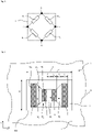
- Fig. 1 shows a cross-section
- Fig. 2 shows a plan view of a vertical Hall device 1 of the prior art.
- axes x and y oriented orthogonally to each other are used to indicate the direction in which a "length" or a "width" is measured. Any distance along the x-axis, such as L in Fig. 2 , will be called a length; and any distance along the y-axis, such as W in Fig. 2 , will be called a width.
- This convention will be applied independently on the ratio of the length and the width of the structure under consideration.
- the vertical Hall device 1 is fabricated with an IC (integrated circuit) technology: It has an N-type region 2 which is implanted into a P-type region 3 which may be a P-type substrate. Four heavily doped N + regions arranged along a straight line 8 are disposed at the surface of the N-well NW and form electrical contacts 4 to 7.
- the N-well NW has a depth d NW
- the N + contacts have a depth d + .
- the vertical Hall device 1 has a length L and a width W. Two non-neighboring contacts of the vertical Hall device 1 are used as input terminals and the other two non-neighboring contacts are used as output terminals.
- the contacts 4 and 6 can be used as the input terminals and the contacts 5 and 7 as the output terminals, or vice versa.
- the electrical resistances R 1 , R 2 , R 3 and R 4 between the contacts 4 to 7 of the Hall device 1 can be represented by a Wheatstone bridge as shown in fig. 3 .
- the Hall device 1 is supplied with a constant current I in or with a constant voltage V in via the input terminals. If the Hall device 1 is exposed to a magnetic field having a component perpendicular to the effective device plane, then the electromotive force of the Hall effect acts between the output terminals. The voltage V out , which appears between the output terminals, is called the output voltage of the Hall device 1.
- V out V off + S l ⁇ I in ⁇ B
- V out V off + S V ⁇ V in ⁇ B
- V off denotes an offset voltage
- S l denotes the current-related sensitivity
- B denotes the component of a magnetic field perpendicular to the effective device plane
- S V denotes the voltage-related sensitivity
- a Hall device In order to be suitable for a practical application as a magnetic field sensor, a Hall device should have the following main characteristics:
- the requirements a) through c) will be met if the four resistances R 1 , R 2 , R 3 , R 4 are all approximately equal.
- the voltage-related magnetic sensitivity (requirement d) is a complex function of the characteristics of the material used for the Hall device and of its geometry. But roughly speaking, the requirement d) is easier to meet if the resistances R 1 , R 2 , R 3 , R 4 have equal values and are "short". Here "short” means that the length of a resistor is not greater than the square root of its cross-sectional area.
- the flicker noise (requirement e) depends much on the quality of the material used for the Hall device, and on the quality and protection of its surface.
- any two-dimensional (planar) horizontal Hall device can be transformed by a mathematical technique known as conformal mapping into a vertical Hall device. But the calculated dimensions of the contacts are nearly impossible to meet in reality.
- a vertical Hall device was fist described in US patent no. 4782375 . This device has five contacts arranged along a line, the two outermost of them being short-circuited. When designed properly, the five-contact vertical Hall device may meet the requirements a), d), and e); but it is much more difficult to meet the requirements b) and c) with the known five-contact structures.
- the four-contact vertical Hall device disclosed in US patent no. 5057890 intrinsically meets the exchangeability requirement c). But when implemented by using IC technology, the four-contact vertical Hall device usually has a very big offset and a low voltage-related magnetic sensitivity; that is, the requirements a) and d) are not met.
- US 2010/0219810 discloses a five-contact vertical Hall device which comprises a doped substrate, a doped central island extending downwardly within the doped substrate from an upper surface of the doped substrate and two doped outer islands extending downwardly within the doped substrate from the upper surface of the doped substrate.
- the outer islands are electrically isolated from the central island within an upper portion of the substrate and electrically coupled to the central island within a lower portion of the substrate. These contacts are used to supply the Hall current.
- the Hall device further comprises two doped contacts within the central island which are used to tap the Hall voltage.
- US 2013/0021026 discloses an electronic device including a number of n Hall effect regions with n>1, wherein the n Hall effect regions are isolated from each other.
- the electronic device also includes at least eight contacts in or on surfaces of the n Hall effect regions, wherein the contacts include: a first and a second contact of each Hall effect region.
- the at least eight contacts include at least two supply contacts and at least two sense contacts.
- Each Hall effect region includes at most one of the at least two supply contacts and at most one of the at least two sense contacts.
- US 4829352 discloses a Hall element comprising a plurality of interconnected portions formed in a common semiconductor layer. Depending on how the portions are interconnected, the Hall element may detect the sum or difference of magnetic field values.
- US 2010/0164483 discloses a horizontal Hall element which can be used in combination with a magnetic field concentrator to measure the same components of the magnetic field that two vertical Hall devices can measure.
- the invention concerns a four-contact or five-contact vertical Hall device with the contacts arranged along a straight line on the surface of a deep N-well.
- the four-contact vertical Hall device has two inner contacts and two outer contacts. The contacts are formed of highly doped N + regions.
- the five-contact vertical Hall device additionally has a central contact placed between the two inner contacts.
- the two outer contacts of the five-contact vertical Hall device are short-circuited, e.g. by a metal line which directly connects the two outer contacts.
- the two inner contacts have a same length and a same width and the two outer contacts have a same length and a same width.
- Both, the four-contact vertical Hall device and the five-contact vertical Hall device are symmetrical with respect to a first symmetry line and a central symmetry plane which extends orthogonally to the first symmetry line.
- the object of the invention is to develop a vertical Hall device, which fulfills all the above requirements a) through e) and which can be fabricated by using the process of a commercially available silicon CMOS integrated circuit technology.
- the invention proposes a novel layout of integrated four- and five-contact vertical Hall-effect devices, which allows for equating the values of the resistances R 1 , R 2 , R 3 , R 4 as well as for achieving high magnetic sensitivity of the Hall device without the need to add separate fabrication steps to an existing silicon CMOS technology.
- the invention proposes new designs for vertical Hall devices as follows which reduce the resistance R 4 and/or increase the resistance R 2 (The reference numbers refer to Figs. 1 and 2 ):
- the effective width of the outer contacts is bigger than the effective width of the inner contacts.
- the resulting effective width of the vertical Hall device along its length is therefore non-uniform, smaller near the inner contacts and larger toward the outer contacts. This design reduces the resistance R 4 between the outer contacts.
- a P + stripe is disposed between the inner contacts 5 and 6.
- the P + stripe does not touch the N + regions of the inner contacts.
- the P + stripe is a heavily doped P + area.
- the length of the P + stripe is selected so that its distance to the inner contacts is smaller than the minimum distance allowed by the design rules of the used IC technology. This design increases the resistance R 2 between the inner contacts.
- the resistance R 4 is reduced according to the first embodiment by making the effective width of the outer contacts bigger than the effective width of the inner contacts and the resistance R 2 is increased according to the second embodiment by disposing a P + stripe between the inner contacts.
- the effective width of the outer contacts is bigger than the effective width of the inner contacts and the effective width of the central contact is the same as or, preferably, less than the effective width of the inner contacts.
- the resulting effective width of the vertical Hall device along its length is non-uniform, smaller near the central contact and larger toward the outer contacts. This design reduces the resistance R 4 between an outer contact and the inner contact that is farthest away from this outer contact.
- a P + stripe is disposed between the central contact and each of its neighbouring inner contacts.
- the two P + stripes do not touch the N + areas of the neighbouring contacts.
- the length of the two P + stripes is preferably selected so that their distance to the neighbouring N + contacts is smaller than the minimum distance allowed by the design rules of the used IC technology. This design increases resistances between the inner contacts and the central contact.
- the P + stripes of this embodiment may be also added to the vertical Hall device of the first embodiment.
- the effective width of the inner contacts may be defined by the course of an inner edge of an additional deep P-well ring.
- the width of the opening of the deep P-well ring which is enclosed by the inner edge of the deep P-well ring is bigger at the outer contacts than as at the inner contacts.
- the deep P-well ring has a depth that is less than the depth of the deep N-well. Because the lateral diffusion of the deep P-well ring is smaller than the lateral diffusion of the deep N-well ring, the shape of the active zone contributing most to the magnetic sensitivity of the vertical Hall device is better defined.
- the term "effective width" of a contact has the meaning that it is not the width of the contact at the surface of the N+ region that counts but the width of the area where the deep N-well and the highly doped N + region forming the contact merge into one another.
- variable width of the vertical Hall device of the invention along its length is different from all known designs of prior art vertical Hall devices, where the width W is constant as illustrated in Fig. 2 .
- the width W of the vertical Hall device corresponds to the thickness of a conventional horizontal Hall device.
- the horizontal Hall devices always have a uniform thickness of the active layer. Obviously, the uniformity of the width W of the vertical Hall devices has been considered a rule by analogy with the horizontal Hall devices. The invention breaks with this rule.
- variable width of the vertical Hall device of the invention along its length means that the active zone of the Hall device is significantly three-dimensional, whereas the active zone of the vertical Hall devices of the prior art is essentially two-dimensional (the active zone lies in the plane XZ of Fig. 3 ).
- the shallow P + stripe (or stripes) eliminates some negative effects originating from the three-dimensional structure of the N + contacts, and makes them behave like two-dimensional contacts (which is in the plane XY of Fig. 3 ).
- the essence of the invention is the improvement of the characteristics of vertical Hall devices by A) transforming some parts of its active zone from a two dimensional structure into a three dimensional structure, and B) transforming some other parts of its active zone from a three dimensional structure into a two dimensional structure. The best results are achieved when the measures A) and B) are combined.
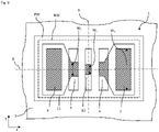
- Fig. 4 shows a plan view of a first embodiment of a four-contact vertical Hall device 1 according to the invention.
- the vertical Hall device 1 is manufactured for example by the well-known CMOS technology and comprises a deep N-well NW embedded in a low-doped P-type substrate 3 (with substrate doping PS).
- the deep N-well NW has preferably a rectangular shape of length L and width W.
- the vertical Hall device 1 has four electrical contacts 4-7 disposed at the surface of the N-well NW and arranged along a first symmetry line 8 and symmetrically with respect to a symmetry plane 9.
- the symmetry line 8 is a straight line and runs orthogonally to the symmetry plane 9.
- the electrical contacts 4-7 are formed of highly doped N + regions which are contacted in conventional manner by metal lines (not shown).
- the electrical contacts 4-7 have approximately rectangular shapes.
- the inner contacts 5, 6 have a same length l 6 and a same width w 2 and the outer contacts 4, 5 have a same length l 7 and a same width w 4 .
- the width w 2 of the inner contacts 5 and 6 is smaller than the width w 4 of the outer contacts 4 and 5, namely: w 2 ⁇ w 4
- the effective widths of the resistances - seen in plan view - are very different.
- the regions of the resistances R 1 to R 4 in Fig. 4 are of three-dimensional nature, with complicated current distributions, they can be approximated by simple shapes: in plan view, the resistances R 1 and R 3 appear as trapezoides having a middle width w 1 , and the resistances R 2 and R 4 appear as rectangles having widths w 2 and w 4 , respectively, with w 2 ⁇ w 4 .
- R 4 >>R 2 , i.e., R 4 / R 2 >> 1. If the length L and all the other lengths of the vertical Hall devices shown in Figs. 1 and 4 are kept the same, the fact that now w 2 ⁇ w 4 means that the ratio of the resistors R 4 / R 2 is reduced, namely R 4 / R 2 invention ⁇ R 4 / R 2 prior art
- the ratio of the widths w 4 and w 2 is at least w 4 /w 2 > 1.2
- variable thickness also has a beneficial influence on the ratio of the resistances R 1 and R 3 with the resistances R 2 and R 4 .
- Figure 5 shows a plan view a) and two cross-sections b) and c) of a second embodiment of a four-contact vertical Hall device 1 according to the invention.
- the design of this vertical Hall device differs from the vertical Hall device 1 shown in Fig. 4 in that the effective width of the inner contacts 5 and 6 is defined by an additional appropriately shaped P-well ring PW and not by the nominal width of the N + regions.
- the P-well ring PW is made of a moderately doped P-type area.
- the average doping of the N + regions, deep P-well and deep N-well is chosen such that Doping N + ⁇ Doping PW ⁇ Doping NW
- the width of the N + regions at the surface of the N-well NW is equal for all N + regions but that the width of the inner contacts 5 and 6 in the depth ranging from d + to d PW is smaller than the width of the outer contacts 4 and 7 in this depth range.
- This facilitates contacting the N + regions with metal lines (not shown), which occurs at the surface of the device, but reduces the effective width of the inner contacts 5 and 6.
- the effective width of a contact is the width of the area where the N + region contacts the deep N-well NW.
- FIG. 5 a illustrates the size of the contacts 4 to 7 at the surface of the chip while the hatched area inside the borderline illustrates the effective contact area at the depth d PW below the surface of the chip.
- the effective width is therefore smaller for the inner contacts 5 and 6 than for the outer contacts 4 and 7.
- Figs. 5 b) and 5 c show the cross sections of the vertical Hall device 1 along the lines S 1 and S 2 shown in Fig. 5 a ), respectively.
- the depths d + and d PW of the N + regions and the deep P-well ring PW are chosen so that d + ⁇ d PW .
- the doping profiles shown in Figs. 5 b ) and c) illustrate that the effective width w 2 of the contacts 5 and 6 is smaller than the effective width w 4 of the contacts 4 and 7.
- the shape of the inner edge 11 of the P-well ring PW is chosen so that P-well ring PW channels the current flowing between the input terminals into the areas denoted in Fig. 5 a ) by A 1 , A 2 , A 3 and A 4 .
- This is indicated by the facts that the width of the electrical contacts between the N + regions of the inner contacts 5, 6 and of the adjacent part of the deep N-well NW are small - see w 2 in Fig. 5 b ) and that the width of the contacts between the N + regions of the outer contacts 4, 7 and of the adjacent part of the deep N-well NW are large - see w 4 in Fig. 5 c ).
- the width of the resistance R 4 is essentially given by the width w of the deep N-well NW, as indicated in Fig. 5 c ). So in spite of the fact that the distance between the outer contacts 4 and 7 is larger than the distance between the inner contacts 5 and 6, since the widths of the conductive regions of the deep N-well NW between these pairs of contacts are also different with a convenient proportion, namely w 4 > w 2 , the resistances between these two pairs of contacts can be made similar, that is R 4 ⁇ R 2 .
- the application of the additional deep P-well ring PW of the described shape helps achieving the equality of the resistances R 1 , R 2 , R 3 and R 4 . Moreover, forcing the current between the inner contacts 5 and 6 into a channel of narrow width w 2 results in increasing the current-related sensitivity of the vertical Hall device 1.
- Fig. 6 shows a plan view of a third embodiment of a four-contact vertical Hall device according to the invention.
- the only difference with respect to the second embodiment shown in Fig. 5 a ) is a different shape of the inner edge 11 of the deep P-well ring PW. But the essential features of the embodiments shown in Figs. 5 and 6 are the same.
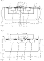
- Fig. 7 shows a cross-section of a fourth embodiment of a four-contact vertical Hall device 1 according to the invention.
- the vertical Hall device 1 has a P + stripe 10 disposed between the N + regions of the inner contacts 5 and 6.
- the P + stripe 10 is implemented by using a shallow highly doped P-type layer having a depth approximately equal to the depth d + of the N + layer.
- the P + stripe 10 has a length L P+ which is chosen such that the P + stripe 10 does not touch the neighbouring contacts 5 or 6 and 12, i.e. the P + stripe 10 and the inner neighbouring contacts 5 or 6 and 12 are separated by distances L P5 and L P6 , respectively.
- the separation between the P + region of the P + stripe 10 and the N + regions of the neighbouring contacts 5 or 6 and 12 is needed in order to avoid a tunnelling current between these regions. Since the P + stripe 10 is surrounded by N-type material, it is isolated from it by a depletion layer. This depletion layer prohibits a lateral current to flow between the adjacent side walls of the N + regions of the contacts 5 or 6 and 12. In other words, the conduction path indicated by the resistance R 2 ' in Fig. 2 is eliminated. By doing so, the resulting resistance R b between the inner contact 5 or 6 and the central contacts 12 increases and it becomes easier to equate the resistances R a and R b .
- a deep P-well PW shaped as shown in Figs. 5 and 6 may be used to define the width of the active zone and also the width of the contacts 5 and 6 or of all contacts 4 to 7.
- the deep N-well NW can be a ring that is shaped like the deep P-well ring PW.
- five-contact vertical Hall elements can be designed straightforward in an analogous way in order to reduce the respective resistances R a , R d ; and/or to increase the resistances R b and R c see Fig. 8 for these resistances.
- Fig. 8 shows a cross-section of a five-contact vertical Hall device 1.
- the five-contact vertical Hall device 1 has a deep N-well NW, two inner contacts 5, 6 and two outer contacts 4, 7 and a central contact 12 disposed between the inner contacts 5 and 6.
- the contacts 4 to 7 and 12 are disposed at a surface of the deep N-well NW and arranged along a straight symmetry line.
- the two inner contacts 5 and 6 have a same length and a same width and the two outer contacts 4 and 7 have a same length and a same width.
- the inner contacts 5 and 6 and the outer contacts 4 and 7 are disposed symmetrically with respect to the central contact 12.
- the two outer contacts 4 and 7 are short-circuited, e.g. by connecting them directly through a metal line 13 (shown symbolically).
- the metal line 13 serves then as one of the terminals of the Hall device as it short circuits the contacts 4 and 7.
- the vertical line 13 serves then as one of the terminals of the Hall device as it short circuits the
- the Hall device 1 either the contact 12 and the metal line 13 are used as input terminals and the contacts 5 and 6 as output terminals, or the contacts 5 and 6 are used as input terminals and the contact 12 and the metal line 13 as output terminals.
- the resistances Ra, Rb, Rc and Rd symbolize the electrical resistances between the said terminals of the device.
- Fig. 8 illustrates an embodiment of the five-contact vertical Hall device 1 according to the invention wherein a P + stripe 10 is disposed between each of the inner contacts 5 and 6 and the central contact 12.
- the P + stripes 10 are separated from the respective neighbouring inner contact 5, 6 and the central contact 12 by a distance.
- the P + stripes 10 increase the resistance R b between the contacts 5 and 12, and the resistance R c between the contacts 12 and 6, while keeping a small distance l 2 , as determined by conformal mapping.
- a deep P-well PW may be used to define the width of the active zone and also the width of the contacts 5, 6 and 12 or 4 to 7 and 12.
- the effective width w 4 of the outer contacts 4, 7 is bigger than the effective width of the inner contacts 5, 6 which is slightly larger than w 2 .
- This can be achieved by making the width of the N + regions of the inner contacts 5 and 6 and the central contact 12 smaller than the width of the N + regions of the outer contacts 4 and 7 analogously to the embodiment of the four-contact vertical Hall device 1 shown in Fig. 4 , or, as shown in Fig. 9 , by adding a deep P-well ring PW wherein the inner edge 11 of the deep P-well ring PW is appropriately shaped.
- the effective width w 5 of the central contact 12 is smaller than the effective width of the inner contacts 5 and 6 which is slightly larger than w 2 , but the width of the central contract 12 may also be the same as the effective width of the inner contacts 5 and 6.
- the P + stripes 10 shown in Fig. 8 may also be added to the vertical Hall device 1 shown in Fig. 9 .
- the vertical Hall devices 1 are fabricated using a 0.35 ⁇ m "high voltage CMOS technology" which provides the following doping layers:
Landscapes
- Physics & Mathematics (AREA)
- Condensed Matter Physics & Semiconductors (AREA)
- General Physics & Mathematics (AREA)
- Hall/Mr Elements (AREA)
- Measuring Magnetic Variables (AREA)
Claims (8)
- Capteur à effet Hall vertical à quatre contacts ayant un puits N profond (NW) et un premier contact extérieur (4), un premier contact intérieur (5), un second contact intérieur (6) et un second contact extérieur (7) disposés à une surface du puits N profond (NW) et disposés dans cet ordre le long d'une ligne de symétrie droite (8) et symétriquement par rapport à un plan de symétrie central (9), dans lequel chacun des contacts (4-7) est formé d'une région N+ fortement dopée, dans lequel les deux contacts intérieurs (5, 6) ont une même longueur et une même largeur effective et les deux contacts extérieurs (4, 7) ont une même longueur et une même largeur effective, dans lequel les longueurs sont mesurées le long de la ligne de symétrie droite (8) et les largeurs sont mesurées orthogonalement à la ligne de symétrie droite (8), et dans lequel le premier contact extérieur (4) et le second contact intérieur (6) sont utilisés comme bornes d'entrée et le premier contact intérieur (5) et le second contact extérieur (7) sont utilisés comme bornes de sortie ou le premier contact intérieur (5) et le second contact extérieur (7) sont utilisés comme bornes d'entrée et le premier contact extérieur (4) et le second contact intérieur (6) sont utilisés comme bornes de sortie, caractérisé en ce que la largeur effective des contacts extérieurs (4, 7) est plus grande que la largeur effective des contacts intérieurs (5, 6), dans lequel la largeur effective d'un contact est la largeur de la zone où la région N+ fortement dopée formant le contact et le puits N profond (NW) se rejoignent.
- Capteur à effet Hall vertical selon la revendication 1, caractérisé en ce que la largeur nominale des contacts extérieurs (4, 7) est supérieure à la largeur nominale des contacts intérieurs (5, 6), dans lequel la largeur nominale d'un contact est la largeur à la surface du puits N profond (NW).
- Capteur à effet Hall vertical selon la revendication 1, comprenant en outre un anneau de puits P (PW), dans lequel une largeur d'un bord intérieur (11) de l'anneau de puits P (PW) est plus grande aux contacts extérieurs (4, 7) qu'aux contacts intérieurs (5, 6).
- Capteur à effet Hall vertical selon l'une quelconque des revendications 1 à 3, caractérisé en ce qu'une bande P+ (10) est disposée entre les contacts intérieurs (5, 6), la bande P+ (10) étant séparée des contacts intérieurs (5, 6) par une distance.
- Capteur à effet Hall vertical à cinq contacts ayant un puits N profond (NW) et un premier contact extérieur (4), un premier contact intérieur (5), un contact central (12), un second contact intérieur (6) et un second contact extérieur (7) disposés à une surface du puits N profond (NW) et dans cet ordre le long d'une ligne de symétrie droite (8), dans lequel chacun des contacts (4-7, 12) est formé d'une région N+ fortement dopée, dans lequel les deux contacts intérieurs (5, 6) sont disposés symétriquement par rapport au contact central (12) et les deux contacts extérieurs (4, 7) sont disposés symétriquement par rapport au contact central (12), dans lequel les deux contacts intérieurs (5, 6) ont une même longueur et une même largeur effective et les deux contacts extérieurs (4, 7) ont une même longueur et une même largeur effective, dans lequel les longueurs sont mesurées le long de la ligne de symétrie droite (8) et les largeurs sont mesurées orthogonalement à la ligne de symétrie droite (8), dans lequel les deux contacts extérieurs (4, 7) sont court-circuités et dans lequel les deux contacts extérieurs (4, 7) et le contact central (12) sont utilisés comme bornes d'entrée et les deux contacts intérieurs (5, 6) sont utilisés comme bornes de sortie ou les deux contacts intérieurs (5, 6) sont utilisés comme bornes d'entrée et les deux contacts extérieurs (4, 7) et le contact central (12) sont utilisés comme bornes de sortie, caractérisé en ce que la largeur effective des contacts extérieurs (4, 7) est supérieure à la largeur effective des contacts intérieurs (5, 6), la largeur effective d'un contact étant la largeur de la zone où la région N+ fortement dopée formant le contact et le puits N profond (NW) se rejoignent.
- Capteur à effet Hall vertical selon la revendication 5, caractérisé en ce que la largeur nominale des contacts extérieurs (4, 7) est supérieure à la largeur nominale des contacts intérieurs (5, 6) et du contact central (12), la largeur nominale d'un contact étant la largeur à la surface du puits N profond (NW).
- Capteur à effet Hall vertical selon la revendication 5, comprenant en outre une anneau à puits P (PW), dans lequel une largeur d'un bord intérieur (11) de l'anneau à puits P (PW) est plus grande aux contacts extérieurs (4, 7) qu'aux contacts intérieurs (5, 6) et au contact central (12).
- Capteur à effet Hall vertical selon l'une quelconque des revendications 5 à 7, caractérisé en ce qu'une bande P+ (10) est disposée entre le contact central (12) et le premier contact intérieur (5) ou le deuxième contact intérieur (6) et une autre bande P+ (10) est disposée entre le contact central (12) et l'autre des contacts intérieurs (5, 6), les deux bandes P+ (10) étant séparées du contact central (12) et du contact intérieur voisin respectif (5, 6) par une distance.
Priority Applications (4)
| Application Number | Priority Date | Filing Date | Title |
|---|---|---|---|
| EP14176835.8A EP2966462B1 (fr) | 2014-07-11 | 2014-07-11 | Capteur à effet Hall vertical |
| JP2015133595A JP6726448B2 (ja) | 2014-07-11 | 2015-07-02 | 縦型ホール素子 |
| US14/794,439 US9496487B2 (en) | 2014-07-11 | 2015-07-08 | Vertical hall device |
| CN201510401886.5A CN105261697B (zh) | 2014-07-11 | 2015-07-09 | 垂直霍尔器件 |
Applications Claiming Priority (1)
| Application Number | Priority Date | Filing Date | Title |
|---|---|---|---|
| EP14176835.8A EP2966462B1 (fr) | 2014-07-11 | 2014-07-11 | Capteur à effet Hall vertical |
Publications (2)
| Publication Number | Publication Date |
|---|---|
| EP2966462A1 EP2966462A1 (fr) | 2016-01-13 |
| EP2966462B1 true EP2966462B1 (fr) | 2022-04-20 |
Family
ID=51176218
Family Applications (1)
| Application Number | Title | Priority Date | Filing Date |
|---|---|---|---|
| EP14176835.8A Active EP2966462B1 (fr) | 2014-07-11 | 2014-07-11 | Capteur à effet Hall vertical |
Country Status (4)
| Country | Link |
|---|---|
| US (1) | US9496487B2 (fr) |
| EP (1) | EP2966462B1 (fr) |
| JP (1) | JP6726448B2 (fr) |
| CN (1) | CN105261697B (fr) |
Families Citing this family (3)
| Publication number | Priority date | Publication date | Assignee | Title |
|---|---|---|---|---|
| JP7365771B2 (ja) | 2019-01-31 | 2023-10-20 | エイブリック株式会社 | 半導体装置 |
| CN110736942B (zh) * | 2019-10-12 | 2021-09-10 | 南京邮电大学 | 一种具有对称结构的高灵敏度垂直型磁场传感器 |
| CN117279481B (zh) * | 2023-11-23 | 2024-02-09 | 深圳市晶扬电子有限公司 | 一种高性能垂直型霍尔器件 |
Family Cites Families (15)
| Publication number | Priority date | Publication date | Assignee | Title |
|---|---|---|---|---|
| CH662905A5 (de) | 1983-12-19 | 1987-10-30 | Landis & Gyr Ag | Integrierbares hallelement. |
| CH669068A5 (de) * | 1986-04-29 | 1989-02-15 | Landis & Gyr Ag | Integrierbares hallelement. |
| DE58905956D1 (de) | 1988-09-21 | 1993-11-25 | Landis & Gyr Business Support | Hallelement. |
| JP3602611B2 (ja) * | 1995-03-30 | 2004-12-15 | 株式会社東芝 | 横型ホール素子 |
| DE50215023D1 (de) * | 2002-09-10 | 2011-06-01 | Melexis Tessenderlo Nv | Magnetfeldsensor mit einem hallelement |
| JP2006128400A (ja) * | 2004-10-28 | 2006-05-18 | Denso Corp | 縦型ホール素子 |
| JP4674578B2 (ja) * | 2006-01-13 | 2011-04-20 | 株式会社デンソー | 磁気センサ及び磁気検出方法 |
| JP4994365B2 (ja) * | 2006-04-03 | 2012-08-08 | 旭化成エレクトロニクス株式会社 | ホール素子及び磁気センサ |
| US8114684B2 (en) * | 2009-03-02 | 2012-02-14 | Robert Bosch Gmbh | Vertical hall effect sensor with current focus |
| EP2234185B1 (fr) * | 2009-03-24 | 2012-10-10 | austriamicrosystems AG | Capteur Hall vertical et procédé de production d'un capteur Hall vertical |
| DE102009027338A1 (de) * | 2009-06-30 | 2011-01-05 | Robert Bosch Gmbh | Hall-Sensorelement und Verfahren zur Messung eines Magnetfelds |
| US8829900B2 (en) * | 2011-02-08 | 2014-09-09 | Infineon Technologies Ag | Low offset spinning current hall plate and method to operate it |
| CH704689B1 (de) * | 2011-03-24 | 2016-02-29 | X Fab Semiconductor Foundries | Vertikaler Hallsensor und Verfahren zur Herstellung eines vertikalen Hallsensors. |
| US9007060B2 (en) * | 2011-07-21 | 2015-04-14 | Infineon Technologies Ag | Electronic device with ring-connected hall effect regions |
| CN103698721A (zh) * | 2013-12-30 | 2014-04-02 | 南京大学 | 一种cmos片上三维微型磁检测传感器的霍尔传感单元 |
-
2014
- 2014-07-11 EP EP14176835.8A patent/EP2966462B1/fr active Active
-
2015
- 2015-07-02 JP JP2015133595A patent/JP6726448B2/ja active Active
- 2015-07-08 US US14/794,439 patent/US9496487B2/en active Active
- 2015-07-09 CN CN201510401886.5A patent/CN105261697B/zh active Active
Also Published As
| Publication number | Publication date |
|---|---|
| CN105261697A (zh) | 2016-01-20 |
| JP2016021568A (ja) | 2016-02-04 |
| CN105261697B (zh) | 2019-08-06 |
| EP2966462A1 (fr) | 2016-01-13 |
| JP6726448B2 (ja) | 2020-07-22 |
| US20160013399A1 (en) | 2016-01-14 |
| US9496487B2 (en) | 2016-11-15 |
Similar Documents
| Publication | Publication Date | Title |
|---|---|---|
| TWI521755B (zh) | 具有改良靈敏度的垂直式霍耳效應元件及其製造方法 | |
| DE102009061277B3 (de) | Hall-Effekt-Bauelement, Betriebsverfahren hierfür und Magnetfelderfassungsverfahren | |
| US10247788B2 (en) | Resistive element | |
| DE102012201727B4 (de) | Hallplatte mit niedrigem spinning-strom-versatz und verfahren zum betreiben derselben | |
| US8839677B2 (en) | Stress sensing devices and methods | |
| US9735345B2 (en) | Vertical hall effect sensor | |
| EP2746799B1 (fr) | Capteurs de champ magnétique à semi-conducteur | |
| KR101755698B1 (ko) | 홀 센서 | |
| US11205748B2 (en) | 3-contact vertical hall sensor elements connected in a ring and related devices, systems, and methods | |
| DE102006061883A1 (de) | Magnetsensor und Verfahren zur Magnetfelderfassung | |
| DE102012212606A1 (de) | Vertikaler hall-sensor mit hoher elektrischer symmetrie | |
| CN105607017B (zh) | 三触点霍尔效应设备的系统和布置及相关方法 | |
| EP2966462B1 (fr) | Capteur à effet Hall vertical | |
| JPH01251763A (ja) | 縦型ホール素子と集積化磁気センサ | |
| DE102005008724B4 (de) | Sensor zum Messen eines Magnetfeldes | |
| EP3282484B1 (fr) | Résistance commandée en tension | |
| KR20200004246A (ko) | 반도체 장치 | |
| Huang et al. | Sensitivity Improvement of a Fully Symmetric Vertical Hall Device Fabricated in 0.18 μm Low-Voltage CMOS Technology | |
| CN115643786A (zh) | 半导体装置及半导体装置的制造方法 |
Legal Events
| Date | Code | Title | Description |
|---|---|---|---|
| PUAI | Public reference made under article 153(3) epc to a published international application that has entered the european phase |
Free format text: ORIGINAL CODE: 0009012 |
|
| AK | Designated contracting states |
Kind code of ref document: A1 Designated state(s): AL AT BE BG CH CY CZ DE DK EE ES FI FR GB GR HR HU IE IS IT LI LT LU LV MC MK MT NL NO PL PT RO RS SE SI SK SM TR |
|
| AX | Request for extension of the european patent |
Extension state: BA ME |
|
| 17P | Request for examination filed |
Effective date: 20160330 |
|
| RBV | Designated contracting states (corrected) |
Designated state(s): AL AT BE BG CH CY CZ DE DK EE ES FI FR GB GR HR HU IE IS IT LI LT LU LV MC MK MT NL NO PL PT RO RS SE SI SK SM TR |
|
| STAA | Information on the status of an ep patent application or granted ep patent |
Free format text: STATUS: EXAMINATION IS IN PROGRESS |
|
| 17Q | First examination report despatched |
Effective date: 20190611 |
|
| STAA | Information on the status of an ep patent application or granted ep patent |
Free format text: STATUS: EXAMINATION IS IN PROGRESS |
|
| GRAP | Despatch of communication of intention to grant a patent |
Free format text: ORIGINAL CODE: EPIDOSNIGR1 |
|
| STAA | Information on the status of an ep patent application or granted ep patent |
Free format text: STATUS: GRANT OF PATENT IS INTENDED |
|
| INTG | Intention to grant announced |
Effective date: 20211008 |
|
| GRAJ | Information related to disapproval of communication of intention to grant by the applicant or resumption of examination proceedings by the epo deleted |
Free format text: ORIGINAL CODE: EPIDOSDIGR1 |
|
| STAA | Information on the status of an ep patent application or granted ep patent |
Free format text: STATUS: EXAMINATION IS IN PROGRESS |
|
| GRAP | Despatch of communication of intention to grant a patent |
Free format text: ORIGINAL CODE: EPIDOSNIGR1 |
|
| STAA | Information on the status of an ep patent application or granted ep patent |
Free format text: STATUS: GRANT OF PATENT IS INTENDED |
|
| INTC | Intention to grant announced (deleted) | ||
| GRAS | Grant fee paid |
Free format text: ORIGINAL CODE: EPIDOSNIGR3 |
|
| INTG | Intention to grant announced |
Effective date: 20220215 |
|
| GRAA | (expected) grant |
Free format text: ORIGINAL CODE: 0009210 |
|
| STAA | Information on the status of an ep patent application or granted ep patent |
Free format text: STATUS: THE PATENT HAS BEEN GRANTED |
|
| AK | Designated contracting states |
Kind code of ref document: B1 Designated state(s): AL AT BE BG CH CY CZ DE DK EE ES FI FR GB GR HR HU IE IS IT LI LT LU LV MC MK MT NL NO PL PT RO RS SE SI SK SM TR |
|
| REG | Reference to a national code |
Ref country code: GB Ref legal event code: FG4D |
|
| REG | Reference to a national code |
Ref country code: CH Ref legal event code: EP |
|
| REG | Reference to a national code |
Ref country code: DE Ref legal event code: R096 Ref document number: 602014083307 Country of ref document: DE |
|
| REG | Reference to a national code |
Ref country code: IE Ref legal event code: FG4D |
|
| REG | Reference to a national code |
Ref country code: AT Ref legal event code: REF Ref document number: 1485559 Country of ref document: AT Kind code of ref document: T Effective date: 20220515 |
|
| REG | Reference to a national code |
Ref country code: LT Ref legal event code: MG9D |
|
| REG | Reference to a national code |
Ref country code: NL Ref legal event code: MP Effective date: 20220420 |
|
| REG | Reference to a national code |
Ref country code: AT Ref legal event code: MK05 Ref document number: 1485559 Country of ref document: AT Kind code of ref document: T Effective date: 20220420 |
|
| PG25 | Lapsed in a contracting state [announced via postgrant information from national office to epo] |
Ref country code: NL Free format text: LAPSE BECAUSE OF FAILURE TO SUBMIT A TRANSLATION OF THE DESCRIPTION OR TO PAY THE FEE WITHIN THE PRESCRIBED TIME-LIMIT Effective date: 20220420 |
|
| PG25 | Lapsed in a contracting state [announced via postgrant information from national office to epo] |
Ref country code: SE Free format text: LAPSE BECAUSE OF FAILURE TO SUBMIT A TRANSLATION OF THE DESCRIPTION OR TO PAY THE FEE WITHIN THE PRESCRIBED TIME-LIMIT Effective date: 20220420 Ref country code: PT Free format text: LAPSE BECAUSE OF FAILURE TO SUBMIT A TRANSLATION OF THE DESCRIPTION OR TO PAY THE FEE WITHIN THE PRESCRIBED TIME-LIMIT Effective date: 20220822 Ref country code: NO Free format text: LAPSE BECAUSE OF FAILURE TO SUBMIT A TRANSLATION OF THE DESCRIPTION OR TO PAY THE FEE WITHIN THE PRESCRIBED TIME-LIMIT Effective date: 20220720 Ref country code: LT Free format text: LAPSE BECAUSE OF FAILURE TO SUBMIT A TRANSLATION OF THE DESCRIPTION OR TO PAY THE FEE WITHIN THE PRESCRIBED TIME-LIMIT Effective date: 20220420 Ref country code: HR Free format text: LAPSE BECAUSE OF FAILURE TO SUBMIT A TRANSLATION OF THE DESCRIPTION OR TO PAY THE FEE WITHIN THE PRESCRIBED TIME-LIMIT Effective date: 20220420 Ref country code: GR Free format text: LAPSE BECAUSE OF FAILURE TO SUBMIT A TRANSLATION OF THE DESCRIPTION OR TO PAY THE FEE WITHIN THE PRESCRIBED TIME-LIMIT Effective date: 20220721 Ref country code: FI Free format text: LAPSE BECAUSE OF FAILURE TO SUBMIT A TRANSLATION OF THE DESCRIPTION OR TO PAY THE FEE WITHIN THE PRESCRIBED TIME-LIMIT Effective date: 20220420 Ref country code: ES Free format text: LAPSE BECAUSE OF FAILURE TO SUBMIT A TRANSLATION OF THE DESCRIPTION OR TO PAY THE FEE WITHIN THE PRESCRIBED TIME-LIMIT Effective date: 20220420 Ref country code: BG Free format text: LAPSE BECAUSE OF FAILURE TO SUBMIT A TRANSLATION OF THE DESCRIPTION OR TO PAY THE FEE WITHIN THE PRESCRIBED TIME-LIMIT Effective date: 20220720 Ref country code: AT Free format text: LAPSE BECAUSE OF FAILURE TO SUBMIT A TRANSLATION OF THE DESCRIPTION OR TO PAY THE FEE WITHIN THE PRESCRIBED TIME-LIMIT Effective date: 20220420 |
|
| PG25 | Lapsed in a contracting state [announced via postgrant information from national office to epo] |
Ref country code: RS Free format text: LAPSE BECAUSE OF FAILURE TO SUBMIT A TRANSLATION OF THE DESCRIPTION OR TO PAY THE FEE WITHIN THE PRESCRIBED TIME-LIMIT Effective date: 20220420 Ref country code: PL Free format text: LAPSE BECAUSE OF FAILURE TO SUBMIT A TRANSLATION OF THE DESCRIPTION OR TO PAY THE FEE WITHIN THE PRESCRIBED TIME-LIMIT Effective date: 20220420 Ref country code: LV Free format text: LAPSE BECAUSE OF FAILURE TO SUBMIT A TRANSLATION OF THE DESCRIPTION OR TO PAY THE FEE WITHIN THE PRESCRIBED TIME-LIMIT Effective date: 20220420 Ref country code: IS Free format text: LAPSE BECAUSE OF FAILURE TO SUBMIT A TRANSLATION OF THE DESCRIPTION OR TO PAY THE FEE WITHIN THE PRESCRIBED TIME-LIMIT Effective date: 20220820 |
|
| REG | Reference to a national code |
Ref country code: DE Ref legal event code: R097 Ref document number: 602014083307 Country of ref document: DE |
|
| PG25 | Lapsed in a contracting state [announced via postgrant information from national office to epo] |
Ref country code: SM Free format text: LAPSE BECAUSE OF FAILURE TO SUBMIT A TRANSLATION OF THE DESCRIPTION OR TO PAY THE FEE WITHIN THE PRESCRIBED TIME-LIMIT Effective date: 20220420 Ref country code: SK Free format text: LAPSE BECAUSE OF FAILURE TO SUBMIT A TRANSLATION OF THE DESCRIPTION OR TO PAY THE FEE WITHIN THE PRESCRIBED TIME-LIMIT Effective date: 20220420 Ref country code: RO Free format text: LAPSE BECAUSE OF FAILURE TO SUBMIT A TRANSLATION OF THE DESCRIPTION OR TO PAY THE FEE WITHIN THE PRESCRIBED TIME-LIMIT Effective date: 20220420 Ref country code: EE Free format text: LAPSE BECAUSE OF FAILURE TO SUBMIT A TRANSLATION OF THE DESCRIPTION OR TO PAY THE FEE WITHIN THE PRESCRIBED TIME-LIMIT Effective date: 20220420 Ref country code: DK Free format text: LAPSE BECAUSE OF FAILURE TO SUBMIT A TRANSLATION OF THE DESCRIPTION OR TO PAY THE FEE WITHIN THE PRESCRIBED TIME-LIMIT Effective date: 20220420 Ref country code: CZ Free format text: LAPSE BECAUSE OF FAILURE TO SUBMIT A TRANSLATION OF THE DESCRIPTION OR TO PAY THE FEE WITHIN THE PRESCRIBED TIME-LIMIT Effective date: 20220420 |
|
| PLBE | No opposition filed within time limit |
Free format text: ORIGINAL CODE: 0009261 |
|
| STAA | Information on the status of an ep patent application or granted ep patent |
Free format text: STATUS: NO OPPOSITION FILED WITHIN TIME LIMIT |
|
| PG25 | Lapsed in a contracting state [announced via postgrant information from national office to epo] |
Ref country code: MC Free format text: LAPSE BECAUSE OF FAILURE TO SUBMIT A TRANSLATION OF THE DESCRIPTION OR TO PAY THE FEE WITHIN THE PRESCRIBED TIME-LIMIT Effective date: 20220420 |
|
| 26N | No opposition filed |
Effective date: 20230123 |
|
| REG | Reference to a national code |
Ref country code: BE Ref legal event code: MM Effective date: 20220731 |
|
| PG25 | Lapsed in a contracting state [announced via postgrant information from national office to epo] |
Ref country code: AL Free format text: LAPSE BECAUSE OF FAILURE TO SUBMIT A TRANSLATION OF THE DESCRIPTION OR TO PAY THE FEE WITHIN THE PRESCRIBED TIME-LIMIT Effective date: 20220420 |
|
| PG25 | Lapsed in a contracting state [announced via postgrant information from national office to epo] |
Ref country code: LU Free format text: LAPSE BECAUSE OF NON-PAYMENT OF DUE FEES Effective date: 20220711 |
|
| PG25 | Lapsed in a contracting state [announced via postgrant information from national office to epo] |
Ref country code: SI Free format text: LAPSE BECAUSE OF FAILURE TO SUBMIT A TRANSLATION OF THE DESCRIPTION OR TO PAY THE FEE WITHIN THE PRESCRIBED TIME-LIMIT Effective date: 20220420 Ref country code: BE Free format text: LAPSE BECAUSE OF NON-PAYMENT OF DUE FEES Effective date: 20220731 |
|
| PG25 | Lapsed in a contracting state [announced via postgrant information from national office to epo] |
Ref country code: IE Free format text: LAPSE BECAUSE OF NON-PAYMENT OF DUE FEES Effective date: 20220711 |
|
| PGFP | Annual fee paid to national office [announced via postgrant information from national office to epo] |
Ref country code: IT Payment date: 20230727 Year of fee payment: 10 Ref country code: GB Payment date: 20230720 Year of fee payment: 10 Ref country code: CH Payment date: 20230801 Year of fee payment: 10 |
|
| PGFP | Annual fee paid to national office [announced via postgrant information from national office to epo] |
Ref country code: FR Payment date: 20230721 Year of fee payment: 10 Ref country code: DE Payment date: 20230724 Year of fee payment: 10 |
|
| PG25 | Lapsed in a contracting state [announced via postgrant information from national office to epo] |
Ref country code: HU Free format text: LAPSE BECAUSE OF FAILURE TO SUBMIT A TRANSLATION OF THE DESCRIPTION OR TO PAY THE FEE WITHIN THE PRESCRIBED TIME-LIMIT; INVALID AB INITIO Effective date: 20140711 |
|
| PG25 | Lapsed in a contracting state [announced via postgrant information from national office to epo] |
Ref country code: MK Free format text: LAPSE BECAUSE OF FAILURE TO SUBMIT A TRANSLATION OF THE DESCRIPTION OR TO PAY THE FEE WITHIN THE PRESCRIBED TIME-LIMIT Effective date: 20220420 Ref country code: CY Free format text: LAPSE BECAUSE OF FAILURE TO SUBMIT A TRANSLATION OF THE DESCRIPTION OR TO PAY THE FEE WITHIN THE PRESCRIBED TIME-LIMIT Effective date: 20220420 |